POWER — Power supply
This device has the following power supply features:
- On-chip LDO and DC/DC regulators
- Global System ON/OFF modes with individual RAM section power control
- Analog or digital pin wakeup from System OFF
- Supervisor HW to manage power on reset, brownout, and power fail
- Auto-controlled refresh modes for LDO and DC/DC regulators to maximize efficiency
- Automatic switching between LDO and DC/DC regulator based on load to maximize efficiency
Regulators
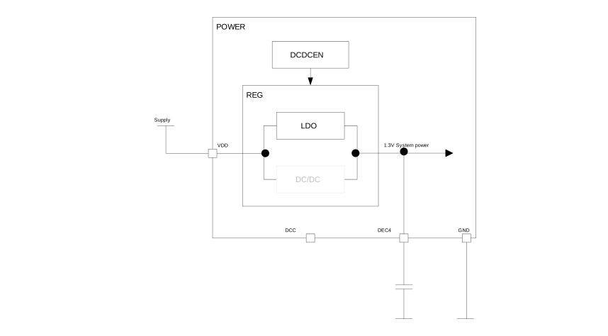
- Internal LDO regulator
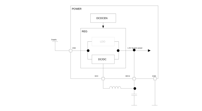
- Internal DC/DC regulator
The LDO is the default regulator.
The DC/DC regulator can be used as an alternative to the LDO regulator and is enabled through the DCDCEN register. Using the DC/DC regulator will reduce current consumption compared to when using the LDO regulator, but the DC/DC regulator requires an external LC filter to be connected, as shown in DC/DC regulator setup.
System OFF mode
System OFF is the deepest power saving mode the system can enter. In this mode, the system’s core functionality is powered down and all ongoing tasks are terminated.
The device can be put into System OFF mode using the register SYSTEMOFF. When in System OFF mode, the device can be woken up through one of the following signals:
- The DETECT signal, optionally generated by the GPIO peripheral
- A reset
When the system wakes up from System OFF mode, it gets reset. For more details, see Reset behavior.
One or more RAM sections can be retained in System OFF mode, depending on the settings in the RAM[n].POWER registers.
RAM[n].POWER are retained registers, see Reset behavior. These registers are usually overwritten by the startup code provided with the nRF application examples.
Before entering System OFF mode, the user must make sure that all on-going EasyDMA transactions have been completed. This is usually accomplished by making sure that the EasyDMA enabled peripheral is not active when entering System OFF.
Emulated System OFF mode
If the device is in debug interface mode, System OFF will be emulated to secure that all required resources needed for debugging are available during System OFF.
System ON mode
System ON is the default state after power-on reset. In System ON, all functional blocks such as the CPU or peripherals can be in IDLE or RUN mode, depending on the configuration set by the software and the state of the application executing.
Register RESETREAS provides information about the source causing the wakeup or reset.
The system can switch the appropriate internal power sources on and off, depending on how much power is needed at any given time. The power requirement of a peripheral is directly related to its activity level, and the activity level of a peripheral is usually raised and lowered when specific tasks are triggered or events are generated.
Sub power modes
In System ON mode, when both the CPU and all the peripherals are in IDLE mode, the system can reside in one of the two sub power modes.
The sub power modes are:
- Constant Latency
- Low-power
In Constant Latency mode, the CPU wakeup latency and the PPI task response are constant and kept at a minimum. This is secured by forcing a set of basic resources to be turned on while in sleep. Having a constant and predictable latency is at the cost of having increased power consumption. The Constant Latency mode is selected by triggering the CONSTLAT task.
In Low-power mode, the automatic power management system described in System ON mode ensures that the most efficient supply option is chosen to save most power. Having the lowest power possible is at the cost of having a varying CPU wakeup latency and PPI task response. The Low-power mode is selected by triggering the LOWPWR task.
When the system enters System ON mode, it is by default in Low-power sub power mode.
Power supply supervisor
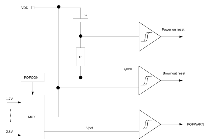
The power supply supervisor initializes the system at power-on and provides an early warning of impending power failure.
In addition, the power supply supervisor puts the system in a reset state if the supply voltage is too low for safe operation (brownout). The power supply supervisor is illustrated in Power supply supervisor.
Power-fail comparator
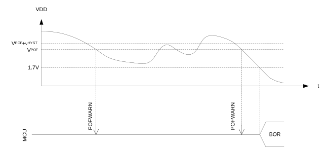
The power-fail comparator (POF) can provide the CPU with an early warning of impending power failure. It will not reset the system, but give the CPU time to prepare for an orderly power-down.
The comparator features a hysteresis of VHYST, as illustrated in Power-fail comparator (BOR = Brownout reset). The threshold VPOF is set in register POFCON. If the POF is enabled and the supply voltage falls below VPOF, the POFWARN event will be generated. This event will also be generated if the supply voltage is already below VPOF at the time the POF is enabled, or if VPOF is re-configured to a level above the supply voltage.
If power-fail warning is enabled and the supply voltage is below VPOF the power-fail comparator will prevent the NVMC from performing write operations to the NVM. See NVMC — Non-volatile memory controller for more information about the NVMC.
To save power, the power-fail comparator is not active in System OFF or in System ON when HFCLK is not running.
RAM power control
The RAM power control registers are used for configuring the following:
- The RAM sections to be retained during System OFF
- The RAM sections to be retained and accessible during System ON
In System OFF, retention of a RAM section is configured in the RETENTION field of the corresponding RAM[n] register.
In System ON, retention and accessibility for a RAM section is configured in the RETENTION and POWER fields of the corresponding RAM[n] register.
The following table summarizes the behavior of these registers.
| Configuration | RAM section status | |||
|---|---|---|---|---|
| System on/off | RAM[n].POWER.POWER | RAM[n].POWER.RETENTION | Accessible | Retained |
| Off | x | Off | No | No |
| Off | x | On | No | Yes |
| On | Off | Off | No | No |
| On | Off1 | On | No | Yes |
| On | On | x | Yes | Yes |
The advantage of not retaining RAM contents is that the overall current consumption is reduced.
See chapter Memory for more information on RAM sections.
Reset
There are multiple sources that may trigger a reset.
After a reset has occurred, register RESETREAS can be read to determine which source generated the reset.
Power-on reset
The power-on reset generator initializes the system at power-on.
The system is held in reset state until the supply has reached the minimum operating voltage and the internal voltage regulators have started.
A step increase in supply voltage of 300 mV or more, with rise time of 300 ms or less, within the valid supply range, may result in a system reset.
Pin reset
A pin reset is generated when the physical reset pin on the device is asserted.
Pin reset is configured via the PSELRESET[n] registers.
Wakeup from System OFF mode reset
The device is reset when it wakes up from System OFF mode.
The debug access port (DAP) is not reset following a wake up from System OFF mode if the device is in Debug Interface mode. See chapter Debug for more information.
Soft reset
A soft reset is generated when the SYSRESETREQ bit of the Application Interrupt and Reset Control Register (AIRCR register) in the ARM® core is set.
Refer to ARM documentation for more details.
A soft reset can also be generated via the RESET register in the CTRL-AP.
Watchdog reset
A Watchdog reset is generated when the watchdog times out.
See chapter WDT — Watchdog timer for more information.
Brown-out reset
The brown-out reset generator puts the system in reset state if the supply voltage drops below the brownout reset (BOR) threshold.
Refer to section Power fail comparator for more information.
Retained registers
A retained register is a register that will retain its value in System OFF mode and through a reset, depending on reset source. See individual peripheral chapters for information of which registers are retained for the various peripherals.
Reset behavior
Registers
| Base address | Peripheral | Instance | Description | Configuration | |
|---|---|---|---|---|---|
| 0x40000000 | POWER | POWER | Power control | For 24 kB RAM variant, only RAM[0].x to RAM[2].x registers are in use. | |
| Register | Offset | Description | |
|---|---|---|---|
| TASKS_CONSTLAT | 0x078 | Enable Constant Latency mode | |
| TASKS_LOWPWR | 0x07C | Enable Low-power mode (variable latency) | |
| EVENTS_POFWARN | 0x108 | Power failure warning | |
| EVENTS_SLEEPENTER | 0x114 | CPU entered WFI/WFE sleep | |
| EVENTS_SLEEPEXIT | 0x118 | CPU exited WFI/WFE sleep | |
| INTENSET | 0x304 | Enable interrupt | |
| INTENCLR | 0x308 | Disable interrupt | |
| RESETREAS | 0x400 | Reset reason | |
| SYSTEMOFF | 0x500 | System OFF register | |
| POFCON | 0x510 | Power failure comparator configuration | |
| GPREGRET | 0x51C | General purpose retention register | |
| GPREGRET2 | 0x520 | General purpose retention register | |
| DCDCEN | 0x578 | DC/DC enable register | |
| RAM[0].POWER | 0x900 | RAM0 power control register. The RAM size will vary depending on product variant, and the RAM0 register will only be present if the corresponding RAM AHB slave is present on the device. | |
| RAM[0].POWERSET | 0x904 | RAM0 power control set register | |
| RAM[0].POWERCLR | 0x908 | RAM0 power control clear register | |
| RAM[1].POWER | 0x910 | RAM1 power control register. The RAM size will vary depending on product variant, and the RAM1 register will only be present if the corresponding RAM AHB slave is present on the device. | |
| RAM[1].POWERSET | 0x914 | RAM1 power control set register | |
| RAM[1].POWERCLR | 0x918 | RAM1 power control clear register | |
| RAM[2].POWER | 0x920 | RAM2 power control register. The RAM size will vary depending on product variant, and the RAM2 register will only be present if the corresponding RAM AHB slave is present on the device. | |
| RAM[2].POWERSET | 0x924 | RAM2 power control set register | |
| RAM[2].POWERCLR | 0x928 | RAM2 power control clear register | |
| RAM[3].POWER | 0x930 | RAM3 power control register. The RAM size will vary depending on product variant, and the RAM3 register will only be present if the corresponding RAM AHB slave is present on the device. | |
| RAM[3].POWERSET | 0x934 | RAM3 power control set register | |
| RAM[3].POWERCLR | 0x938 | RAM3 power control clear register | |
| RAM[4].POWER | 0x940 | RAM4 power control register. The RAM size will vary depending on product variant, and the RAM4 register will only be present if the corresponding RAM AHB slave is present on the device. | |
| RAM[4].POWERSET | 0x944 | RAM4 power control set register | |
| RAM[4].POWERCLR | 0x948 | RAM4 power control clear register | |
| RAM[5].POWER | 0x950 | RAM5 power control register. The RAM size will vary depending on product variant, and the RAM5 register will only be present if the corresponding RAM AHB slave is present on the device. | |
| RAM[5].POWERSET | 0x954 | RAM5 power control set register | |
| RAM[5].POWERCLR | 0x958 | RAM5 power control clear register | |
| RAM[6].POWER | 0x960 | RAM6 power control register. The RAM size will vary depending on product variant, and the RAM6 register will only be present if the corresponding RAM AHB slave is present on the device. | |
| RAM[6].POWERSET | 0x964 | RAM6 power control set register | |
| RAM[6].POWERCLR | 0x968 | RAM6 power control clear register | |
| RAM[7].POWER | 0x970 | RAM7 power control register. The RAM size will vary depending on product variant, and the RAM7 register will only be present if the corresponding RAM AHB slave is present on the device. | |
| RAM[7].POWERSET | 0x974 | RAM7 power control set register | |
| RAM[7].POWERCLR | 0x978 | RAM7 power control clear register | |
TASKS_CONSTLAT
Address offset: 0x078
Enable Constant Latency mode
| Bit number | 31 | 30 | 29 | 28 | 27 | 26 | 25 | 24 | 23 | 22 | 21 | 20 | 19 | 18 | 17 | 16 | 15 | 14 | 13 | 12 | 11 | 10 | 9 | 8 | 7 | 6 | 5 | 4 | 3 | 2 | 1 | 0 | |||
|---|---|---|---|---|---|---|---|---|---|---|---|---|---|---|---|---|---|---|---|---|---|---|---|---|---|---|---|---|---|---|---|---|---|---|---|
| ID | A | ||||||||||||||||||||||||||||||||||
| Reset 0x00000000 | 0 | 0 | 0 | 0 | 0 | 0 | 0 | 0 | 0 | 0 | 0 | 0 | 0 | 0 | 0 | 0 | 0 | 0 | 0 | 0 | 0 | 0 | 0 | 0 | 0 | 0 | 0 | 0 | 0 | 0 | 0 | 0 | |||
| ID | Access | Field | Value ID | Value | Description | ||||||||||||||||||||||||||||||
| A | W | TASKS_CONSTLAT | Enable Constant Latency mode | ||||||||||||||||||||||||||||||||
Trigger | 1 | Trigger task | |||||||||||||||||||||||||||||||||
TASKS_LOWPWR
Address offset: 0x07C
Enable Low-power mode (variable latency)
| Bit number | 31 | 30 | 29 | 28 | 27 | 26 | 25 | 24 | 23 | 22 | 21 | 20 | 19 | 18 | 17 | 16 | 15 | 14 | 13 | 12 | 11 | 10 | 9 | 8 | 7 | 6 | 5 | 4 | 3 | 2 | 1 | 0 | |||
|---|---|---|---|---|---|---|---|---|---|---|---|---|---|---|---|---|---|---|---|---|---|---|---|---|---|---|---|---|---|---|---|---|---|---|---|
| ID | A | ||||||||||||||||||||||||||||||||||
| Reset 0x00000000 | 0 | 0 | 0 | 0 | 0 | 0 | 0 | 0 | 0 | 0 | 0 | 0 | 0 | 0 | 0 | 0 | 0 | 0 | 0 | 0 | 0 | 0 | 0 | 0 | 0 | 0 | 0 | 0 | 0 | 0 | 0 | 0 | |||
| ID | Access | Field | Value ID | Value | Description | ||||||||||||||||||||||||||||||
| A | W | TASKS_LOWPWR | Enable Low-power mode (variable latency) | ||||||||||||||||||||||||||||||||
Trigger | 1 | Trigger task | |||||||||||||||||||||||||||||||||
EVENTS_POFWARN
Address offset: 0x108
Power failure warning
| Bit number | 31 | 30 | 29 | 28 | 27 | 26 | 25 | 24 | 23 | 22 | 21 | 20 | 19 | 18 | 17 | 16 | 15 | 14 | 13 | 12 | 11 | 10 | 9 | 8 | 7 | 6 | 5 | 4 | 3 | 2 | 1 | 0 | |||
|---|---|---|---|---|---|---|---|---|---|---|---|---|---|---|---|---|---|---|---|---|---|---|---|---|---|---|---|---|---|---|---|---|---|---|---|
| ID | A | ||||||||||||||||||||||||||||||||||
| Reset 0x00000000 | 0 | 0 | 0 | 0 | 0 | 0 | 0 | 0 | 0 | 0 | 0 | 0 | 0 | 0 | 0 | 0 | 0 | 0 | 0 | 0 | 0 | 0 | 0 | 0 | 0 | 0 | 0 | 0 | 0 | 0 | 0 | 0 | |||
| ID | Access | Field | Value ID | Value | Description | ||||||||||||||||||||||||||||||
| A | RW | EVENTS_POFWARN | Power failure warning | ||||||||||||||||||||||||||||||||
NotGenerated | 0 | Event not generated | |||||||||||||||||||||||||||||||||
Generated | 1 | Event generated | |||||||||||||||||||||||||||||||||
EVENTS_SLEEPENTER
Address offset: 0x114
CPU entered WFI/WFE sleep
| Bit number | 31 | 30 | 29 | 28 | 27 | 26 | 25 | 24 | 23 | 22 | 21 | 20 | 19 | 18 | 17 | 16 | 15 | 14 | 13 | 12 | 11 | 10 | 9 | 8 | 7 | 6 | 5 | 4 | 3 | 2 | 1 | 0 | |||
|---|---|---|---|---|---|---|---|---|---|---|---|---|---|---|---|---|---|---|---|---|---|---|---|---|---|---|---|---|---|---|---|---|---|---|---|
| ID | A | ||||||||||||||||||||||||||||||||||
| Reset 0x00000000 | 0 | 0 | 0 | 0 | 0 | 0 | 0 | 0 | 0 | 0 | 0 | 0 | 0 | 0 | 0 | 0 | 0 | 0 | 0 | 0 | 0 | 0 | 0 | 0 | 0 | 0 | 0 | 0 | 0 | 0 | 0 | 0 | |||
| ID | Access | Field | Value ID | Value | Description | ||||||||||||||||||||||||||||||
| A | RW | EVENTS_SLEEPENTER | CPU entered WFI/WFE sleep | ||||||||||||||||||||||||||||||||
NotGenerated | 0 | Event not generated | |||||||||||||||||||||||||||||||||
Generated | 1 | Event generated | |||||||||||||||||||||||||||||||||
EVENTS_SLEEPEXIT
Address offset: 0x118
CPU exited WFI/WFE sleep
| Bit number | 31 | 30 | 29 | 28 | 27 | 26 | 25 | 24 | 23 | 22 | 21 | 20 | 19 | 18 | 17 | 16 | 15 | 14 | 13 | 12 | 11 | 10 | 9 | 8 | 7 | 6 | 5 | 4 | 3 | 2 | 1 | 0 | |||
|---|---|---|---|---|---|---|---|---|---|---|---|---|---|---|---|---|---|---|---|---|---|---|---|---|---|---|---|---|---|---|---|---|---|---|---|
| ID | A | ||||||||||||||||||||||||||||||||||
| Reset 0x00000000 | 0 | 0 | 0 | 0 | 0 | 0 | 0 | 0 | 0 | 0 | 0 | 0 | 0 | 0 | 0 | 0 | 0 | 0 | 0 | 0 | 0 | 0 | 0 | 0 | 0 | 0 | 0 | 0 | 0 | 0 | 0 | 0 | |||
| ID | Access | Field | Value ID | Value | Description | ||||||||||||||||||||||||||||||
| A | RW | EVENTS_SLEEPEXIT | CPU exited WFI/WFE sleep | ||||||||||||||||||||||||||||||||
NotGenerated | 0 | Event not generated | |||||||||||||||||||||||||||||||||
Generated | 1 | Event generated | |||||||||||||||||||||||||||||||||
INTENSET
Address offset: 0x304
Enable interrupt
| Bit number | 31 | 30 | 29 | 28 | 27 | 26 | 25 | 24 | 23 | 22 | 21 | 20 | 19 | 18 | 17 | 16 | 15 | 14 | 13 | 12 | 11 | 10 | 9 | 8 | 7 | 6 | 5 | 4 | 3 | 2 | 1 | 0 | |||
|---|---|---|---|---|---|---|---|---|---|---|---|---|---|---|---|---|---|---|---|---|---|---|---|---|---|---|---|---|---|---|---|---|---|---|---|
| ID | C | B | A | ||||||||||||||||||||||||||||||||
| Reset 0x00000000 | 0 | 0 | 0 | 0 | 0 | 0 | 0 | 0 | 0 | 0 | 0 | 0 | 0 | 0 | 0 | 0 | 0 | 0 | 0 | 0 | 0 | 0 | 0 | 0 | 0 | 0 | 0 | 0 | 0 | 0 | 0 | 0 | |||
| ID | Access | Field | Value ID | Value | Description | ||||||||||||||||||||||||||||||
| A | RW | POFWARN | Write '1' to enable interrupt for event POFWARN | ||||||||||||||||||||||||||||||||
Set | 1 | Enable | |||||||||||||||||||||||||||||||||
Disabled | 0 | Read: Disabled | |||||||||||||||||||||||||||||||||
Enabled | 1 | Read: Enabled | |||||||||||||||||||||||||||||||||
| B | RW | SLEEPENTER | Write '1' to enable interrupt for event SLEEPENTER | ||||||||||||||||||||||||||||||||
Set | 1 | Enable | |||||||||||||||||||||||||||||||||
Disabled | 0 | Read: Disabled | |||||||||||||||||||||||||||||||||
Enabled | 1 | Read: Enabled | |||||||||||||||||||||||||||||||||
| C | RW | SLEEPEXIT | Write '1' to enable interrupt for event SLEEPEXIT | ||||||||||||||||||||||||||||||||
Set | 1 | Enable | |||||||||||||||||||||||||||||||||
Disabled | 0 | Read: Disabled | |||||||||||||||||||||||||||||||||
Enabled | 1 | Read: Enabled | |||||||||||||||||||||||||||||||||
INTENCLR
Address offset: 0x308
Disable interrupt
| Bit number | 31 | 30 | 29 | 28 | 27 | 26 | 25 | 24 | 23 | 22 | 21 | 20 | 19 | 18 | 17 | 16 | 15 | 14 | 13 | 12 | 11 | 10 | 9 | 8 | 7 | 6 | 5 | 4 | 3 | 2 | 1 | 0 | |||
|---|---|---|---|---|---|---|---|---|---|---|---|---|---|---|---|---|---|---|---|---|---|---|---|---|---|---|---|---|---|---|---|---|---|---|---|
| ID | C | B | A | ||||||||||||||||||||||||||||||||
| Reset 0x00000000 | 0 | 0 | 0 | 0 | 0 | 0 | 0 | 0 | 0 | 0 | 0 | 0 | 0 | 0 | 0 | 0 | 0 | 0 | 0 | 0 | 0 | 0 | 0 | 0 | 0 | 0 | 0 | 0 | 0 | 0 | 0 | 0 | |||
| ID | Access | Field | Value ID | Value | Description | ||||||||||||||||||||||||||||||
| A | RW | POFWARN | Write '1' to disable interrupt for event POFWARN | ||||||||||||||||||||||||||||||||
Clear | 1 | Disable | |||||||||||||||||||||||||||||||||
Disabled | 0 | Read: Disabled | |||||||||||||||||||||||||||||||||
Enabled | 1 | Read: Enabled | |||||||||||||||||||||||||||||||||
| B | RW | SLEEPENTER | Write '1' to disable interrupt for event SLEEPENTER | ||||||||||||||||||||||||||||||||
Clear | 1 | Disable | |||||||||||||||||||||||||||||||||
Disabled | 0 | Read: Disabled | |||||||||||||||||||||||||||||||||
Enabled | 1 | Read: Enabled | |||||||||||||||||||||||||||||||||
| C | RW | SLEEPEXIT | Write '1' to disable interrupt for event SLEEPEXIT | ||||||||||||||||||||||||||||||||
Clear | 1 | Disable | |||||||||||||||||||||||||||||||||
Disabled | 0 | Read: Disabled | |||||||||||||||||||||||||||||||||
Enabled | 1 | Read: Enabled | |||||||||||||||||||||||||||||||||
RESETREAS
Address offset: 0x400
Reset reason
Unless cleared, the RESETREAS register will be cumulative. A field is cleared by writing '1' to it. If none of the reset sources are flagged, this indicates that the chip was reset from the on-chip reset generator, which will indicate a power-on-reset or a brownout reset.
| Bit number | 31 | 30 | 29 | 28 | 27 | 26 | 25 | 24 | 23 | 22 | 21 | 20 | 19 | 18 | 17 | 16 | 15 | 14 | 13 | 12 | 11 | 10 | 9 | 8 | 7 | 6 | 5 | 4 | 3 | 2 | 1 | 0 | |||
|---|---|---|---|---|---|---|---|---|---|---|---|---|---|---|---|---|---|---|---|---|---|---|---|---|---|---|---|---|---|---|---|---|---|---|---|
| ID | F | E | D | C | B | A | |||||||||||||||||||||||||||||
| Reset 0x00000000 | 0 | 0 | 0 | 0 | 0 | 0 | 0 | 0 | 0 | 0 | 0 | 0 | 0 | 0 | 0 | 0 | 0 | 0 | 0 | 0 | 0 | 0 | 0 | 0 | 0 | 0 | 0 | 0 | 0 | 0 | 0 | 0 | |||
| ID | Access | Field | Value ID | Value | Description | ||||||||||||||||||||||||||||||
| A | RW | RESETPIN | Reset from pin-reset detected | ||||||||||||||||||||||||||||||||
NotDetected | 0 | Not detected | |||||||||||||||||||||||||||||||||
Detected | 1 | Detected | |||||||||||||||||||||||||||||||||
| B | RW | DOG | Reset from watchdog detected | ||||||||||||||||||||||||||||||||
NotDetected | 0 | Not detected | |||||||||||||||||||||||||||||||||
Detected | 1 | Detected | |||||||||||||||||||||||||||||||||
| C | RW | SREQ | Reset from soft reset detected | ||||||||||||||||||||||||||||||||
NotDetected | 0 | Not detected | |||||||||||||||||||||||||||||||||
Detected | 1 | Detected | |||||||||||||||||||||||||||||||||
| D | RW | LOCKUP | Reset from CPU lock-up detected | ||||||||||||||||||||||||||||||||
NotDetected | 0 | Not detected | |||||||||||||||||||||||||||||||||
Detected | 1 | Detected | |||||||||||||||||||||||||||||||||
| E | RW | OFF | Reset due to wake up from System OFF mode when wakeup is triggered from DETECT signal from GPIO | ||||||||||||||||||||||||||||||||
NotDetected | 0 | Not detected | |||||||||||||||||||||||||||||||||
Detected | 1 | Detected | |||||||||||||||||||||||||||||||||
| F | RW | DIF | Reset due to wake up from System OFF mode when wakeup is triggered from entering into debug interface mode | ||||||||||||||||||||||||||||||||
NotDetected | 0 | Not detected | |||||||||||||||||||||||||||||||||
Detected | 1 | Detected | |||||||||||||||||||||||||||||||||
SYSTEMOFF
Address offset: 0x500
System OFF register
| Bit number | 31 | 30 | 29 | 28 | 27 | 26 | 25 | 24 | 23 | 22 | 21 | 20 | 19 | 18 | 17 | 16 | 15 | 14 | 13 | 12 | 11 | 10 | 9 | 8 | 7 | 6 | 5 | 4 | 3 | 2 | 1 | 0 | |||
|---|---|---|---|---|---|---|---|---|---|---|---|---|---|---|---|---|---|---|---|---|---|---|---|---|---|---|---|---|---|---|---|---|---|---|---|
| ID | A | ||||||||||||||||||||||||||||||||||
| Reset 0x00000000 | 0 | 0 | 0 | 0 | 0 | 0 | 0 | 0 | 0 | 0 | 0 | 0 | 0 | 0 | 0 | 0 | 0 | 0 | 0 | 0 | 0 | 0 | 0 | 0 | 0 | 0 | 0 | 0 | 0 | 0 | 0 | 0 | |||
| ID | Access | Field | Value ID | Value | Description | ||||||||||||||||||||||||||||||
| A | W | SYSTEMOFF | Enable System OFF mode | ||||||||||||||||||||||||||||||||
Enter | 1 | Enable System OFF mode | |||||||||||||||||||||||||||||||||
POFCON
Address offset: 0x510
Power failure comparator configuration
| Bit number | 31 | 30 | 29 | 28 | 27 | 26 | 25 | 24 | 23 | 22 | 21 | 20 | 19 | 18 | 17 | 16 | 15 | 14 | 13 | 12 | 11 | 10 | 9 | 8 | 7 | 6 | 5 | 4 | 3 | 2 | 1 | 0 | |||
|---|---|---|---|---|---|---|---|---|---|---|---|---|---|---|---|---|---|---|---|---|---|---|---|---|---|---|---|---|---|---|---|---|---|---|---|
| ID | B | B | B | B | A | ||||||||||||||||||||||||||||||
| Reset 0x00000000 | 0 | 0 | 0 | 0 | 0 | 0 | 0 | 0 | 0 | 0 | 0 | 0 | 0 | 0 | 0 | 0 | 0 | 0 | 0 | 0 | 0 | 0 | 0 | 0 | 0 | 0 | 0 | 0 | 0 | 0 | 0 | 0 | |||
| ID | Access | Field | Value ID | Value | Description | ||||||||||||||||||||||||||||||
| A | RW | POF | Enable or disable power failure comparator | ||||||||||||||||||||||||||||||||
Disabled | 0 | Disable | |||||||||||||||||||||||||||||||||
Enabled | 1 | Enable | |||||||||||||||||||||||||||||||||
| B | RW | THRESHOLD | Power failure comparator threshold setting | ||||||||||||||||||||||||||||||||
V17 | 4 | Set threshold to 1.7 V | |||||||||||||||||||||||||||||||||
V18 | 5 | Set threshold to 1.8 V | |||||||||||||||||||||||||||||||||
V19 | 6 | Set threshold to 1.9 V | |||||||||||||||||||||||||||||||||
V20 | 7 | Set threshold to 2.0 V | |||||||||||||||||||||||||||||||||
V21 | 8 | Set threshold to 2.1 V | |||||||||||||||||||||||||||||||||
V22 | 9 | Set threshold to 2.2 V | |||||||||||||||||||||||||||||||||
V23 | 10 | Set threshold to 2.3 V | |||||||||||||||||||||||||||||||||
V24 | 11 | Set threshold to 2.4 V | |||||||||||||||||||||||||||||||||
V25 | 12 | Set threshold to 2.5 V | |||||||||||||||||||||||||||||||||
V26 | 13 | Set threshold to 2.6 V | |||||||||||||||||||||||||||||||||
V27 | 14 | Set threshold to 2.7 V | |||||||||||||||||||||||||||||||||
V28 | 15 | Set threshold to 2.8 V | |||||||||||||||||||||||||||||||||
GPREGRET
Address offset: 0x51C
General purpose retention register
| Bit number | 31 | 30 | 29 | 28 | 27 | 26 | 25 | 24 | 23 | 22 | 21 | 20 | 19 | 18 | 17 | 16 | 15 | 14 | 13 | 12 | 11 | 10 | 9 | 8 | 7 | 6 | 5 | 4 | 3 | 2 | 1 | 0 | |||
|---|---|---|---|---|---|---|---|---|---|---|---|---|---|---|---|---|---|---|---|---|---|---|---|---|---|---|---|---|---|---|---|---|---|---|---|
| ID | A | A | A | A | A | A | A | A | |||||||||||||||||||||||||||
| Reset 0x00000000 | 0 | 0 | 0 | 0 | 0 | 0 | 0 | 0 | 0 | 0 | 0 | 0 | 0 | 0 | 0 | 0 | 0 | 0 | 0 | 0 | 0 | 0 | 0 | 0 | 0 | 0 | 0 | 0 | 0 | 0 | 0 | 0 | |||
| ID | Access | Field | Value ID | Value | Description | ||||||||||||||||||||||||||||||
| A | RW | GPREGRET | General purpose retention register This register is a retained register | ||||||||||||||||||||||||||||||||
GPREGRET2
Address offset: 0x520
General purpose retention register
| Bit number | 31 | 30 | 29 | 28 | 27 | 26 | 25 | 24 | 23 | 22 | 21 | 20 | 19 | 18 | 17 | 16 | 15 | 14 | 13 | 12 | 11 | 10 | 9 | 8 | 7 | 6 | 5 | 4 | 3 | 2 | 1 | 0 | |||
|---|---|---|---|---|---|---|---|---|---|---|---|---|---|---|---|---|---|---|---|---|---|---|---|---|---|---|---|---|---|---|---|---|---|---|---|
| ID | A | A | A | A | A | A | A | A | |||||||||||||||||||||||||||
| Reset 0x00000000 | 0 | 0 | 0 | 0 | 0 | 0 | 0 | 0 | 0 | 0 | 0 | 0 | 0 | 0 | 0 | 0 | 0 | 0 | 0 | 0 | 0 | 0 | 0 | 0 | 0 | 0 | 0 | 0 | 0 | 0 | 0 | 0 | |||
| ID | Access | Field | Value ID | Value | Description | ||||||||||||||||||||||||||||||
| A | RW | GPREGRET | General purpose retention register This register is a retained register | ||||||||||||||||||||||||||||||||
DCDCEN
Address offset: 0x578
DC/DC enable register
| Bit number | 31 | 30 | 29 | 28 | 27 | 26 | 25 | 24 | 23 | 22 | 21 | 20 | 19 | 18 | 17 | 16 | 15 | 14 | 13 | 12 | 11 | 10 | 9 | 8 | 7 | 6 | 5 | 4 | 3 | 2 | 1 | 0 | |||
|---|---|---|---|---|---|---|---|---|---|---|---|---|---|---|---|---|---|---|---|---|---|---|---|---|---|---|---|---|---|---|---|---|---|---|---|
| ID | A | ||||||||||||||||||||||||||||||||||
| Reset 0x00000000 | 0 | 0 | 0 | 0 | 0 | 0 | 0 | 0 | 0 | 0 | 0 | 0 | 0 | 0 | 0 | 0 | 0 | 0 | 0 | 0 | 0 | 0 | 0 | 0 | 0 | 0 | 0 | 0 | 0 | 0 | 0 | 0 | |||
| ID | Access | Field | Value ID | Value | Description | ||||||||||||||||||||||||||||||
| A | RW | DCDCEN | Enable or disable DC/DC converter | ||||||||||||||||||||||||||||||||
Disabled | 0 | Disable | |||||||||||||||||||||||||||||||||
Enabled | 1 | Enable | |||||||||||||||||||||||||||||||||
RAM[n].POWER (n=0..7)
Address offset: 0x900 + (n × 0x10)
RAMn power control register. The RAM size will vary depending on product variant, and the RAMn register will only be present if the corresponding RAM AHB slave is present on the device.
| Bit number | 31 | 30 | 29 | 28 | 27 | 26 | 25 | 24 | 23 | 22 | 21 | 20 | 19 | 18 | 17 | 16 | 15 | 14 | 13 | 12 | 11 | 10 | 9 | 8 | 7 | 6 | 5 | 4 | 3 | 2 | 1 | 0 | |||
|---|---|---|---|---|---|---|---|---|---|---|---|---|---|---|---|---|---|---|---|---|---|---|---|---|---|---|---|---|---|---|---|---|---|---|---|
| ID | D | C | B | A | |||||||||||||||||||||||||||||||
| Reset 0x0000FFFF | 0 | 0 | 0 | 0 | 0 | 0 | 0 | 0 | 0 | 0 | 0 | 0 | 0 | 0 | 0 | 0 | 1 | 1 | 1 | 1 | 1 | 1 | 1 | 1 | 1 | 1 | 1 | 1 | 1 | 1 | 1 | 1 | |||
| ID | Access | Field | Value ID | Value | Description | ||||||||||||||||||||||||||||||
| A-B | RW | S[i]POWER (i=0..1) | Keep RAM section Si ON or OFF in System ON mode. RAM sections are always retained when ON, but can also be retained when OFF dependent on the settings in SiRETENTION. All RAM sections will be OFF in System OFF mode. | ||||||||||||||||||||||||||||||||
Off | 0 | Off | |||||||||||||||||||||||||||||||||
On | 1 | On | |||||||||||||||||||||||||||||||||
| C-D | RW | S[i]RETENTION (i=0..1) | Keep retention on RAM section Si when RAM section is in OFF | ||||||||||||||||||||||||||||||||
Off | 0 | Off | |||||||||||||||||||||||||||||||||
On | 1 | On | |||||||||||||||||||||||||||||||||
RAM[n].POWERSET (n=0..7)
Address offset: 0x904 + (n × 0x10)
RAMn power control set register
When read, this register will return the value of the POWER register.
| Bit number | 31 | 30 | 29 | 28 | 27 | 26 | 25 | 24 | 23 | 22 | 21 | 20 | 19 | 18 | 17 | 16 | 15 | 14 | 13 | 12 | 11 | 10 | 9 | 8 | 7 | 6 | 5 | 4 | 3 | 2 | 1 | 0 | |||
|---|---|---|---|---|---|---|---|---|---|---|---|---|---|---|---|---|---|---|---|---|---|---|---|---|---|---|---|---|---|---|---|---|---|---|---|
| ID | D | C | B | A | |||||||||||||||||||||||||||||||
| Reset 0x0000FFFF | 0 | 0 | 0 | 0 | 0 | 0 | 0 | 0 | 0 | 0 | 0 | 0 | 0 | 0 | 0 | 0 | 1 | 1 | 1 | 1 | 1 | 1 | 1 | 1 | 1 | 1 | 1 | 1 | 1 | 1 | 1 | 1 | |||
| ID | Access | Field | Value ID | Value | Description | ||||||||||||||||||||||||||||||
| A-B | W | S[i]POWER (i=0..1) | Keep RAM section Si of RAMn on or off in System ON mode | ||||||||||||||||||||||||||||||||
On | 1 | On | |||||||||||||||||||||||||||||||||
| C-D | W | S[i]RETENTION (i=0..1) | Keep retention on RAM section Si when RAM section is switched off | ||||||||||||||||||||||||||||||||
On | 1 | On | |||||||||||||||||||||||||||||||||
RAM[n].POWERCLR (n=0..7)
Address offset: 0x908 + (n × 0x10)
RAMn power control clear register
When read, this register will return the value of the POWER register.
| Bit number | 31 | 30 | 29 | 28 | 27 | 26 | 25 | 24 | 23 | 22 | 21 | 20 | 19 | 18 | 17 | 16 | 15 | 14 | 13 | 12 | 11 | 10 | 9 | 8 | 7 | 6 | 5 | 4 | 3 | 2 | 1 | 0 | |||
|---|---|---|---|---|---|---|---|---|---|---|---|---|---|---|---|---|---|---|---|---|---|---|---|---|---|---|---|---|---|---|---|---|---|---|---|
| ID | D | C | B | A | |||||||||||||||||||||||||||||||
| Reset 0x0000FFFF | 0 | 0 | 0 | 0 | 0 | 0 | 0 | 0 | 0 | 0 | 0 | 0 | 0 | 0 | 0 | 0 | 1 | 1 | 1 | 1 | 1 | 1 | 1 | 1 | 1 | 1 | 1 | 1 | 1 | 1 | 1 | 1 | |||
| ID | Access | Field | Value ID | Value | Description | ||||||||||||||||||||||||||||||
| A-B | W | S[i]POWER (i=0..1) | Keep RAM section Si of RAMn on or off in System ON mode | ||||||||||||||||||||||||||||||||
Off | 1 | Off | |||||||||||||||||||||||||||||||||
| C-D | W | S[i]RETENTION (i=0..1) | Keep retention on RAM section Si when RAM section is switched off | ||||||||||||||||||||||||||||||||
Off | 1 | Off | |||||||||||||||||||||||||||||||||
Electrical specification
Device startup times
| Symbol | Description | Min. | Typ. | Max. | Units | ||||
|---|---|---|---|---|---|---|---|---|---|
| tPOR | Time in Power on Reset after VDD reaches 1.7 V for all supply voltages and temperatures. Dependent on supply rise time. 7 | ||||||||
| tPOR,10us | VDD rise time 10 µs | 1 | ms | ||||||
| tPOR,10ms | VDD rise time 10 ms | 9 | ms | ||||||
| tPOR,60ms | VDD rise time 60 ms | 23 | ms | ||||||
| tPINR | If a GPIO pin is configured as reset, the maximum time taken to pull up the pin and release reset after power on reset. Dependent on the pin capacitive load (C)8: t=5RC, R = 13 kΩ | ||||||||
| tPINR,500nF | C = 500 nF | 32.5 | ms | ||||||
| tPINR,10uF | C = 10 µF | 650 | ms | ||||||
| tR2ON | Time from reset to ON (CPU execute) | ||||||||
| tR2ON,NOTCONF | If reset pin not configured | tPOR | ms | ||||||
| tR2ON,CONF | If reset pin configured | tPOR + tPINR | ms | ||||||
| tOFF2ON | Time from OFF to CPU execute | 16.5 | µs | ||||||
| tIDLE2CPU | Time from IDLE to CPU execute | 3.0 | µs | ||||||
| tEVTSET,CL1 | Time from HW event to PPI event in Constant Latency System ON mode | 0.0625 | µs | ||||||
| tEVTSET,CL0 | Time from HW event to PPI event in Low Power System ON mode | 0.0625 | µs |
Power fail comparator
| Symbol | Description | Min. | Typ. | Max. | Units | ||||
|---|---|---|---|---|---|---|---|---|---|
| VPOF | Nominal power level warning thresholds (falling supply voltage). Levels are configurable between Min. and Max. in 100 mV increments. | 1.7 | 2.8 | V | |||||
| VPOFTOL | Threshold voltage tolerance | ±1 | ±5 | % | |||||
| VPOFHYST | Threshold voltage hysteresis | 50 | mV | ||||||
| VBOR,OFF | Brown out reset voltage range SYSTEM OFF mode | 1.2 | 1.7 | V | |||||
| VBOR,ON | Brown out reset voltage range SYSTEM ON mode | 1.48 | 1.7 | V |