TWI — I2C compatible two-wire interface
The TWI master is compatible with I2C operating at 100 kHz and 400 kHz.
Functional description
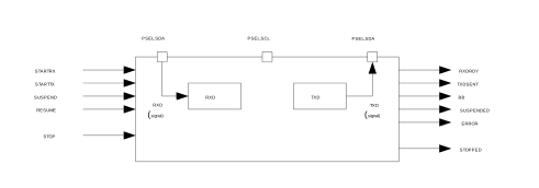
This TWI master is not compatible with CBUS. The TWI transmitter and receiver are single buffered.
See TWI master's main features.
A TWI setup with one master and three slaves is shown in the following figure. This TWI master is only able to operate as the only master on the TWI bus.
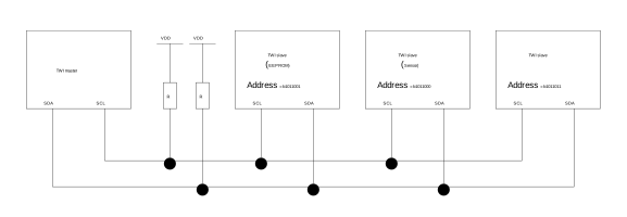
This TWI master supports clock stretching performed by the slaves. The TWI master is started by triggering the STARTTX or STARTRX tasks, and stopped by triggering the STOP task.
If a NACK is clocked in from the slave, the TWI master will generate an ERROR event.
Master mode pin configuration
The different signals SCL and SDA associated with the TWI master are mapped to physical pins according to the configuration specified in the PSEL.SCL and PSEL.SDA registers respectively.
If the CONNECT field of a PSEL.xxx register is set to Disconnected, the associated TWI signal is not connected to any physical pin. The PSEL.SCL and PSEL.SDA registers and their configurations are only used as long as the TWI master is enabled, and retained only as long as the device is in ON mode. PSEL.SCL and PSEL.SDA must only be configured when TWI is disabled.
To secure correct signal levels on the pins used by the TWI master when the system is in OFF mode, and when the TWI master is disabled, these pins must be configured in the GPIO peripheral as described in GPIO configuration.
Only one peripheral can be assigned to drive a particular GPIO pin at a time, failing to do so may result in unpredictable behavior.
| TWI master signal | TWI master pin | Direction | Drive strength | Output value |
|---|---|---|---|---|
| SCL | As specified in PSEL.SCL | Input | S0D1 | Not applicable |
| SDA | As specified in PSEL.SDA | Input | S0D1 | Not applicable |
Shared resources
TWI shares registers and other resources with other peripherals that have the same ID as TWI.
Therefore, you must disable all peripherals that have the same ID as TWI before TWI can be configured and used. Disabling a peripheral that has the same ID as TWI will not reset any of the registers that are shared with TWI. It is therefore important to configure all relevant TWI registers explicitly to secure that it operates correctly.
The Instantiation table in Instantiation shows which peripherals have the same ID as TWI.
Master write sequence
A TWI master write sequence is started by triggering the STARTTX task. After the STARTTX task has been triggered, the TWI master will generate a start condition on the TWI bus, followed by clocking out the address and the READ/WRITE bit set to 0 (WRITE=0, READ=1).
The address must match the address of the slave device that the master wants to write to. The READ/WRITE bit is followed by an ACK/NACK bit (ACK=0 or NACK=1) generated by the slave.
After receiving the ACK bit, the TWI master will clock out the data bytes that are written to the TXD register. Each byte clocked out from the master will be followed by an ACK/NACK bit clocked in from the slave. A TXDSENT event will be generated each time the TWI master has clocked out a TXD byte, and the associated ACK/NACK bit has been clocked in from the slave.
The TWI master transmitter is single buffered. A second byte can only be written to the TXD register after the previous byte has been clocked out and the ACK/NACK bit clocked in, that is, after the TXDSENT event has been generated.
If the CPU is prevented from writing to TXD when the TWI master is ready to clock out a byte, the TWI master will stretch the clock until the CPU has written a byte to the TXD register.
A typical TWI master write sequence is illustrated in The TWI master writing data to a slave. Occurrence 3 in the figure illustrates delayed processing of the TXDSENT event associated with TXD byte 1. In this scenario the TWI master will stretch the clock to prevent writing erroneous data to the slave.
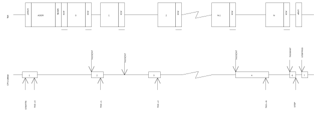
The TWI master write sequence is stopped when the STOP task is triggered, causing the TWI master to generate a stop condition on the TWI bus.
Master read sequence
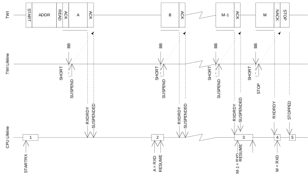
A TWI master read sequence is started by triggering the STARTRX task. After the STARTRX task has been triggered, the TWI master will generate a start condition on the TWI bus, followed by clocking out the address and the READ/WRITE bit set to 1 (WRITE = 0, READ = 1).
The address must match the address of the slave device that the master wants to read from. The READ/WRITE bit is followed by an ACK/NACK bit (ACK=0 or NACK = 1) generated by the slave.
After having sent the ACK bit, the TWI slave will send data to the master using the clock generated by the master.
The TWI master will generate a RXDRDY event every time a new byte is received in the RXD register.
After receiving a byte, the TWI master will delay sending the ACK/NACK bit by stretching the clock until the CPU has extracted the received byte, by reading the RXD register.
The TWI master read sequence is stopped by triggering the STOP task. This task must be triggered before the last byte is extracted from RXD to ensure that the TWI master sends a NACK back to the slave before generating the stop condition.
A typical TWI master read sequence is illustrated in The TWI master reading data from a slave. Occurrence 3 in this figure illustrates delayed processing of the RXDRDY event associated with RXD byte B. In this scenario the TWI master will stretch the clock to prevent the slave from overwriting the contents of the RXD register.
Master repeated start sequence
A typical repeated start sequence is one in which the TWI master writes one byte to the slave followed by reading M bytes from the slave. Any combination and number of transmit and receive sequences can be combined in this fashion. Only one shortcut to STOP can be enabled at any given time.
The following figure shows a repeated start sequence where the TWI master writes one byte, followed by reading M bytes from the slave without performing a stop in-between.
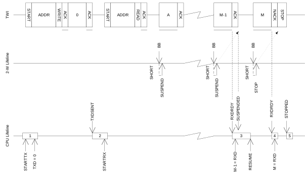
To generate a repeated start after a read sequence, a second start task, STARTRX or STARTTX, must be triggered instead of the STOP task. This start task must be triggered before the last byte is extracted from RXD to ensure that the TWI master sends a NACK back to the slave before generating the repeated start condition.
Low power
When putting the system in low power and the peripheral is not needed, lowest possible power consumption is achieved by stopping, and then disabling the peripheral.
The STOP task is not always needed, like when the peripheral is already stopped. If the STOP task is sent, the software shall wait until the STOPPED event was received as a response before disabling the peripheral through the ENABLE register.
Registers
| Base address | Peripheral | Instance | Description | Configuration | |
|---|---|---|---|---|---|
| 0x40003000 | TWI | TWI0 | Two-wire interface master | Deprecated | |
| Register | Offset | Description | |
|---|---|---|---|
| TASKS_STARTRX | 0x000 | Start TWI receive sequence | |
| TASKS_STARTTX | 0x008 | Start TWI transmit sequence | |
| TASKS_STOP | 0x014 | Stop TWI transaction | |
| TASKS_SUSPEND | 0x01C | Suspend TWI transaction | |
| TASKS_RESUME | 0x020 | Resume TWI transaction | |
| EVENTS_STOPPED | 0x104 | TWI stopped | |
| EVENTS_RXDREADY | 0x108 | TWI RXD byte received | |
| EVENTS_TXDSENT | 0x11C | TWI TXD byte sent | |
| EVENTS_ERROR | 0x124 | TWI error | |
| EVENTS_BB | 0x138 | TWI byte boundary, generated before each byte that is sent or received | |
| EVENTS_SUSPENDED | 0x148 | TWI entered the suspended state | |
| SHORTS | 0x200 | Shortcuts between local events and tasks | |
| INTENSET | 0x304 | Enable interrupt | |
| INTENCLR | 0x308 | Disable interrupt | |
| ERRORSRC | 0x4C4 | Error source | |
| ENABLE | 0x500 | Enable TWI | |
| PSEL.SCL | 0x508 | Pin select for SCL | |
| PSEL.SDA | 0x50C | Pin select for SDA | |
| RXD | 0x518 | RXD register | |
| TXD | 0x51C | TXD register | |
| FREQUENCY | 0x524 | TWI frequency. Accuracy depends on the HFCLK source selected. | |
| ADDRESS | 0x588 | Address used in the TWI transfer | |
TASKS_STARTRX
Address offset: 0x000
Start TWI receive sequence
| Bit number | 31 | 30 | 29 | 28 | 27 | 26 | 25 | 24 | 23 | 22 | 21 | 20 | 19 | 18 | 17 | 16 | 15 | 14 | 13 | 12 | 11 | 10 | 9 | 8 | 7 | 6 | 5 | 4 | 3 | 2 | 1 | 0 | |||
|---|---|---|---|---|---|---|---|---|---|---|---|---|---|---|---|---|---|---|---|---|---|---|---|---|---|---|---|---|---|---|---|---|---|---|---|
| ID | A | ||||||||||||||||||||||||||||||||||
| Reset 0x00000000 | 0 | 0 | 0 | 0 | 0 | 0 | 0 | 0 | 0 | 0 | 0 | 0 | 0 | 0 | 0 | 0 | 0 | 0 | 0 | 0 | 0 | 0 | 0 | 0 | 0 | 0 | 0 | 0 | 0 | 0 | 0 | 0 | |||
| ID | Access | Field | Value ID | Value | Description | ||||||||||||||||||||||||||||||
| A | W | TASKS_STARTRX | Start TWI receive sequence | ||||||||||||||||||||||||||||||||
Trigger | 1 | Trigger task | |||||||||||||||||||||||||||||||||
TASKS_STARTTX
Address offset: 0x008
Start TWI transmit sequence
| Bit number | 31 | 30 | 29 | 28 | 27 | 26 | 25 | 24 | 23 | 22 | 21 | 20 | 19 | 18 | 17 | 16 | 15 | 14 | 13 | 12 | 11 | 10 | 9 | 8 | 7 | 6 | 5 | 4 | 3 | 2 | 1 | 0 | |||
|---|---|---|---|---|---|---|---|---|---|---|---|---|---|---|---|---|---|---|---|---|---|---|---|---|---|---|---|---|---|---|---|---|---|---|---|
| ID | A | ||||||||||||||||||||||||||||||||||
| Reset 0x00000000 | 0 | 0 | 0 | 0 | 0 | 0 | 0 | 0 | 0 | 0 | 0 | 0 | 0 | 0 | 0 | 0 | 0 | 0 | 0 | 0 | 0 | 0 | 0 | 0 | 0 | 0 | 0 | 0 | 0 | 0 | 0 | 0 | |||
| ID | Access | Field | Value ID | Value | Description | ||||||||||||||||||||||||||||||
| A | W | TASKS_STARTTX | Start TWI transmit sequence | ||||||||||||||||||||||||||||||||
Trigger | 1 | Trigger task | |||||||||||||||||||||||||||||||||
TASKS_STOP
Address offset: 0x014
Stop TWI transaction
| Bit number | 31 | 30 | 29 | 28 | 27 | 26 | 25 | 24 | 23 | 22 | 21 | 20 | 19 | 18 | 17 | 16 | 15 | 14 | 13 | 12 | 11 | 10 | 9 | 8 | 7 | 6 | 5 | 4 | 3 | 2 | 1 | 0 | |||
|---|---|---|---|---|---|---|---|---|---|---|---|---|---|---|---|---|---|---|---|---|---|---|---|---|---|---|---|---|---|---|---|---|---|---|---|
| ID | A | ||||||||||||||||||||||||||||||||||
| Reset 0x00000000 | 0 | 0 | 0 | 0 | 0 | 0 | 0 | 0 | 0 | 0 | 0 | 0 | 0 | 0 | 0 | 0 | 0 | 0 | 0 | 0 | 0 | 0 | 0 | 0 | 0 | 0 | 0 | 0 | 0 | 0 | 0 | 0 | |||
| ID | Access | Field | Value ID | Value | Description | ||||||||||||||||||||||||||||||
| A | W | TASKS_STOP | Stop TWI transaction | ||||||||||||||||||||||||||||||||
Trigger | 1 | Trigger task | |||||||||||||||||||||||||||||||||
TASKS_SUSPEND
Address offset: 0x01C
Suspend TWI transaction
| Bit number | 31 | 30 | 29 | 28 | 27 | 26 | 25 | 24 | 23 | 22 | 21 | 20 | 19 | 18 | 17 | 16 | 15 | 14 | 13 | 12 | 11 | 10 | 9 | 8 | 7 | 6 | 5 | 4 | 3 | 2 | 1 | 0 | |||
|---|---|---|---|---|---|---|---|---|---|---|---|---|---|---|---|---|---|---|---|---|---|---|---|---|---|---|---|---|---|---|---|---|---|---|---|
| ID | A | ||||||||||||||||||||||||||||||||||
| Reset 0x00000000 | 0 | 0 | 0 | 0 | 0 | 0 | 0 | 0 | 0 | 0 | 0 | 0 | 0 | 0 | 0 | 0 | 0 | 0 | 0 | 0 | 0 | 0 | 0 | 0 | 0 | 0 | 0 | 0 | 0 | 0 | 0 | 0 | |||
| ID | Access | Field | Value ID | Value | Description | ||||||||||||||||||||||||||||||
| A | W | TASKS_SUSPEND | Suspend TWI transaction | ||||||||||||||||||||||||||||||||
Trigger | 1 | Trigger task | |||||||||||||||||||||||||||||||||
TASKS_RESUME
Address offset: 0x020
Resume TWI transaction
| Bit number | 31 | 30 | 29 | 28 | 27 | 26 | 25 | 24 | 23 | 22 | 21 | 20 | 19 | 18 | 17 | 16 | 15 | 14 | 13 | 12 | 11 | 10 | 9 | 8 | 7 | 6 | 5 | 4 | 3 | 2 | 1 | 0 | |||
|---|---|---|---|---|---|---|---|---|---|---|---|---|---|---|---|---|---|---|---|---|---|---|---|---|---|---|---|---|---|---|---|---|---|---|---|
| ID | A | ||||||||||||||||||||||||||||||||||
| Reset 0x00000000 | 0 | 0 | 0 | 0 | 0 | 0 | 0 | 0 | 0 | 0 | 0 | 0 | 0 | 0 | 0 | 0 | 0 | 0 | 0 | 0 | 0 | 0 | 0 | 0 | 0 | 0 | 0 | 0 | 0 | 0 | 0 | 0 | |||
| ID | Access | Field | Value ID | Value | Description | ||||||||||||||||||||||||||||||
| A | W | TASKS_RESUME | Resume TWI transaction | ||||||||||||||||||||||||||||||||
Trigger | 1 | Trigger task | |||||||||||||||||||||||||||||||||
EVENTS_STOPPED
Address offset: 0x104
TWI stopped
| Bit number | 31 | 30 | 29 | 28 | 27 | 26 | 25 | 24 | 23 | 22 | 21 | 20 | 19 | 18 | 17 | 16 | 15 | 14 | 13 | 12 | 11 | 10 | 9 | 8 | 7 | 6 | 5 | 4 | 3 | 2 | 1 | 0 | |||
|---|---|---|---|---|---|---|---|---|---|---|---|---|---|---|---|---|---|---|---|---|---|---|---|---|---|---|---|---|---|---|---|---|---|---|---|
| ID | A | ||||||||||||||||||||||||||||||||||
| Reset 0x00000000 | 0 | 0 | 0 | 0 | 0 | 0 | 0 | 0 | 0 | 0 | 0 | 0 | 0 | 0 | 0 | 0 | 0 | 0 | 0 | 0 | 0 | 0 | 0 | 0 | 0 | 0 | 0 | 0 | 0 | 0 | 0 | 0 | |||
| ID | Access | Field | Value ID | Value | Description | ||||||||||||||||||||||||||||||
| A | RW | EVENTS_STOPPED | TWI stopped | ||||||||||||||||||||||||||||||||
NotGenerated | 0 | Event not generated | |||||||||||||||||||||||||||||||||
Generated | 1 | Event generated | |||||||||||||||||||||||||||||||||
EVENTS_RXDREADY
Address offset: 0x108
TWI RXD byte received
| Bit number | 31 | 30 | 29 | 28 | 27 | 26 | 25 | 24 | 23 | 22 | 21 | 20 | 19 | 18 | 17 | 16 | 15 | 14 | 13 | 12 | 11 | 10 | 9 | 8 | 7 | 6 | 5 | 4 | 3 | 2 | 1 | 0 | |||
|---|---|---|---|---|---|---|---|---|---|---|---|---|---|---|---|---|---|---|---|---|---|---|---|---|---|---|---|---|---|---|---|---|---|---|---|
| ID | A | ||||||||||||||||||||||||||||||||||
| Reset 0x00000000 | 0 | 0 | 0 | 0 | 0 | 0 | 0 | 0 | 0 | 0 | 0 | 0 | 0 | 0 | 0 | 0 | 0 | 0 | 0 | 0 | 0 | 0 | 0 | 0 | 0 | 0 | 0 | 0 | 0 | 0 | 0 | 0 | |||
| ID | Access | Field | Value ID | Value | Description | ||||||||||||||||||||||||||||||
| A | RW | EVENTS_RXDREADY | TWI RXD byte received | ||||||||||||||||||||||||||||||||
NotGenerated | 0 | Event not generated | |||||||||||||||||||||||||||||||||
Generated | 1 | Event generated | |||||||||||||||||||||||||||||||||
EVENTS_TXDSENT
Address offset: 0x11C
TWI TXD byte sent
| Bit number | 31 | 30 | 29 | 28 | 27 | 26 | 25 | 24 | 23 | 22 | 21 | 20 | 19 | 18 | 17 | 16 | 15 | 14 | 13 | 12 | 11 | 10 | 9 | 8 | 7 | 6 | 5 | 4 | 3 | 2 | 1 | 0 | |||
|---|---|---|---|---|---|---|---|---|---|---|---|---|---|---|---|---|---|---|---|---|---|---|---|---|---|---|---|---|---|---|---|---|---|---|---|
| ID | A | ||||||||||||||||||||||||||||||||||
| Reset 0x00000000 | 0 | 0 | 0 | 0 | 0 | 0 | 0 | 0 | 0 | 0 | 0 | 0 | 0 | 0 | 0 | 0 | 0 | 0 | 0 | 0 | 0 | 0 | 0 | 0 | 0 | 0 | 0 | 0 | 0 | 0 | 0 | 0 | |||
| ID | Access | Field | Value ID | Value | Description | ||||||||||||||||||||||||||||||
| A | RW | EVENTS_TXDSENT | TWI TXD byte sent | ||||||||||||||||||||||||||||||||
NotGenerated | 0 | Event not generated | |||||||||||||||||||||||||||||||||
Generated | 1 | Event generated | |||||||||||||||||||||||||||||||||
EVENTS_ERROR
Address offset: 0x124
TWI error
| Bit number | 31 | 30 | 29 | 28 | 27 | 26 | 25 | 24 | 23 | 22 | 21 | 20 | 19 | 18 | 17 | 16 | 15 | 14 | 13 | 12 | 11 | 10 | 9 | 8 | 7 | 6 | 5 | 4 | 3 | 2 | 1 | 0 | |||
|---|---|---|---|---|---|---|---|---|---|---|---|---|---|---|---|---|---|---|---|---|---|---|---|---|---|---|---|---|---|---|---|---|---|---|---|
| ID | A | ||||||||||||||||||||||||||||||||||
| Reset 0x00000000 | 0 | 0 | 0 | 0 | 0 | 0 | 0 | 0 | 0 | 0 | 0 | 0 | 0 | 0 | 0 | 0 | 0 | 0 | 0 | 0 | 0 | 0 | 0 | 0 | 0 | 0 | 0 | 0 | 0 | 0 | 0 | 0 | |||
| ID | Access | Field | Value ID | Value | Description | ||||||||||||||||||||||||||||||
| A | RW | EVENTS_ERROR | TWI error | ||||||||||||||||||||||||||||||||
NotGenerated | 0 | Event not generated | |||||||||||||||||||||||||||||||||
Generated | 1 | Event generated | |||||||||||||||||||||||||||||||||
EVENTS_BB
Address offset: 0x138
TWI byte boundary, generated before each byte that is sent or received
| Bit number | 31 | 30 | 29 | 28 | 27 | 26 | 25 | 24 | 23 | 22 | 21 | 20 | 19 | 18 | 17 | 16 | 15 | 14 | 13 | 12 | 11 | 10 | 9 | 8 | 7 | 6 | 5 | 4 | 3 | 2 | 1 | 0 | |||
|---|---|---|---|---|---|---|---|---|---|---|---|---|---|---|---|---|---|---|---|---|---|---|---|---|---|---|---|---|---|---|---|---|---|---|---|
| ID | A | ||||||||||||||||||||||||||||||||||
| Reset 0x00000000 | 0 | 0 | 0 | 0 | 0 | 0 | 0 | 0 | 0 | 0 | 0 | 0 | 0 | 0 | 0 | 0 | 0 | 0 | 0 | 0 | 0 | 0 | 0 | 0 | 0 | 0 | 0 | 0 | 0 | 0 | 0 | 0 | |||
| ID | Access | Field | Value ID | Value | Description | ||||||||||||||||||||||||||||||
| A | RW | EVENTS_BB | TWI byte boundary, generated before each byte that is sent or received | ||||||||||||||||||||||||||||||||
NotGenerated | 0 | Event not generated | |||||||||||||||||||||||||||||||||
Generated | 1 | Event generated | |||||||||||||||||||||||||||||||||
EVENTS_SUSPENDED
Address offset: 0x148
TWI entered the suspended state
Generated just after ACK bit has been transferred in a read transaction, and only if SUSPEND has been requested earlier.
| Bit number | 31 | 30 | 29 | 28 | 27 | 26 | 25 | 24 | 23 | 22 | 21 | 20 | 19 | 18 | 17 | 16 | 15 | 14 | 13 | 12 | 11 | 10 | 9 | 8 | 7 | 6 | 5 | 4 | 3 | 2 | 1 | 0 | |||
|---|---|---|---|---|---|---|---|---|---|---|---|---|---|---|---|---|---|---|---|---|---|---|---|---|---|---|---|---|---|---|---|---|---|---|---|
| ID | A | ||||||||||||||||||||||||||||||||||
| Reset 0x00000000 | 0 | 0 | 0 | 0 | 0 | 0 | 0 | 0 | 0 | 0 | 0 | 0 | 0 | 0 | 0 | 0 | 0 | 0 | 0 | 0 | 0 | 0 | 0 | 0 | 0 | 0 | 0 | 0 | 0 | 0 | 0 | 0 | |||
| ID | Access | Field | Value ID | Value | Description | ||||||||||||||||||||||||||||||
| A | RW | EVENTS_SUSPENDED | TWI entered the suspended state Generated just after ACK bit has been transferred in a read transaction, and only if SUSPEND has been requested earlier. | ||||||||||||||||||||||||||||||||
NotGenerated | 0 | Event not generated | |||||||||||||||||||||||||||||||||
Generated | 1 | Event generated | |||||||||||||||||||||||||||||||||
SHORTS
Address offset: 0x200
Shortcuts between local events and tasks
| Bit number | 31 | 30 | 29 | 28 | 27 | 26 | 25 | 24 | 23 | 22 | 21 | 20 | 19 | 18 | 17 | 16 | 15 | 14 | 13 | 12 | 11 | 10 | 9 | 8 | 7 | 6 | 5 | 4 | 3 | 2 | 1 | 0 | |||
|---|---|---|---|---|---|---|---|---|---|---|---|---|---|---|---|---|---|---|---|---|---|---|---|---|---|---|---|---|---|---|---|---|---|---|---|
| ID | B | A | |||||||||||||||||||||||||||||||||
| Reset 0x00000000 | 0 | 0 | 0 | 0 | 0 | 0 | 0 | 0 | 0 | 0 | 0 | 0 | 0 | 0 | 0 | 0 | 0 | 0 | 0 | 0 | 0 | 0 | 0 | 0 | 0 | 0 | 0 | 0 | 0 | 0 | 0 | 0 | |||
| ID | Access | Field | Value ID | Value | Description | ||||||||||||||||||||||||||||||
| A | RW | BB_SUSPEND | |||||||||||||||||||||||||||||||||
Disabled | 0 | Disable shortcut | |||||||||||||||||||||||||||||||||
Enabled | 1 | Enable shortcut | |||||||||||||||||||||||||||||||||
| B | RW | BB_STOP | |||||||||||||||||||||||||||||||||
Disabled | 0 | Disable shortcut | |||||||||||||||||||||||||||||||||
Enabled | 1 | Enable shortcut | |||||||||||||||||||||||||||||||||
INTENSET
Address offset: 0x304
Enable interrupt
| Bit number | 31 | 30 | 29 | 28 | 27 | 26 | 25 | 24 | 23 | 22 | 21 | 20 | 19 | 18 | 17 | 16 | 15 | 14 | 13 | 12 | 11 | 10 | 9 | 8 | 7 | 6 | 5 | 4 | 3 | 2 | 1 | 0 | |||
|---|---|---|---|---|---|---|---|---|---|---|---|---|---|---|---|---|---|---|---|---|---|---|---|---|---|---|---|---|---|---|---|---|---|---|---|
| ID | F | E | D | C | B | A | |||||||||||||||||||||||||||||
| Reset 0x00000000 | 0 | 0 | 0 | 0 | 0 | 0 | 0 | 0 | 0 | 0 | 0 | 0 | 0 | 0 | 0 | 0 | 0 | 0 | 0 | 0 | 0 | 0 | 0 | 0 | 0 | 0 | 0 | 0 | 0 | 0 | 0 | 0 | |||
| ID | Access | Field | Value ID | Value | Description | ||||||||||||||||||||||||||||||
| A | RW | STOPPED | Write '1' to enable interrupt for event STOPPED | ||||||||||||||||||||||||||||||||
Set | 1 | Enable | |||||||||||||||||||||||||||||||||
Disabled | 0 | Read: Disabled | |||||||||||||||||||||||||||||||||
Enabled | 1 | Read: Enabled | |||||||||||||||||||||||||||||||||
| B | RW | RXDREADY | Write '1' to enable interrupt for event RXDREADY | ||||||||||||||||||||||||||||||||
Set | 1 | Enable | |||||||||||||||||||||||||||||||||
Disabled | 0 | Read: Disabled | |||||||||||||||||||||||||||||||||
Enabled | 1 | Read: Enabled | |||||||||||||||||||||||||||||||||
| C | RW | TXDSENT | Write '1' to enable interrupt for event TXDSENT | ||||||||||||||||||||||||||||||||
Set | 1 | Enable | |||||||||||||||||||||||||||||||||
Disabled | 0 | Read: Disabled | |||||||||||||||||||||||||||||||||
Enabled | 1 | Read: Enabled | |||||||||||||||||||||||||||||||||
| D | RW | ERROR | Write '1' to enable interrupt for event ERROR | ||||||||||||||||||||||||||||||||
Set | 1 | Enable | |||||||||||||||||||||||||||||||||
Disabled | 0 | Read: Disabled | |||||||||||||||||||||||||||||||||
Enabled | 1 | Read: Enabled | |||||||||||||||||||||||||||||||||
| E | RW | BB | Write '1' to enable interrupt for event BB | ||||||||||||||||||||||||||||||||
Set | 1 | Enable | |||||||||||||||||||||||||||||||||
Disabled | 0 | Read: Disabled | |||||||||||||||||||||||||||||||||
Enabled | 1 | Read: Enabled | |||||||||||||||||||||||||||||||||
| F | RW | SUSPENDED | Write '1' to enable interrupt for event SUSPENDED Generated just after ACK bit has been transferred in a read transaction, and only if SUSPEND has been requested earlier. | ||||||||||||||||||||||||||||||||
Set | 1 | Enable | |||||||||||||||||||||||||||||||||
Disabled | 0 | Read: Disabled | |||||||||||||||||||||||||||||||||
Enabled | 1 | Read: Enabled | |||||||||||||||||||||||||||||||||
INTENCLR
Address offset: 0x308
Disable interrupt
| Bit number | 31 | 30 | 29 | 28 | 27 | 26 | 25 | 24 | 23 | 22 | 21 | 20 | 19 | 18 | 17 | 16 | 15 | 14 | 13 | 12 | 11 | 10 | 9 | 8 | 7 | 6 | 5 | 4 | 3 | 2 | 1 | 0 | |||
|---|---|---|---|---|---|---|---|---|---|---|---|---|---|---|---|---|---|---|---|---|---|---|---|---|---|---|---|---|---|---|---|---|---|---|---|
| ID | F | E | D | C | B | A | |||||||||||||||||||||||||||||
| Reset 0x00000000 | 0 | 0 | 0 | 0 | 0 | 0 | 0 | 0 | 0 | 0 | 0 | 0 | 0 | 0 | 0 | 0 | 0 | 0 | 0 | 0 | 0 | 0 | 0 | 0 | 0 | 0 | 0 | 0 | 0 | 0 | 0 | 0 | |||
| ID | Access | Field | Value ID | Value | Description | ||||||||||||||||||||||||||||||
| A | RW | STOPPED | Write '1' to disable interrupt for event STOPPED | ||||||||||||||||||||||||||||||||
Clear | 1 | Disable | |||||||||||||||||||||||||||||||||
Disabled | 0 | Read: Disabled | |||||||||||||||||||||||||||||||||
Enabled | 1 | Read: Enabled | |||||||||||||||||||||||||||||||||
| B | RW | RXDREADY | Write '1' to disable interrupt for event RXDREADY | ||||||||||||||||||||||||||||||||
Clear | 1 | Disable | |||||||||||||||||||||||||||||||||
Disabled | 0 | Read: Disabled | |||||||||||||||||||||||||||||||||
Enabled | 1 | Read: Enabled | |||||||||||||||||||||||||||||||||
| C | RW | TXDSENT | Write '1' to disable interrupt for event TXDSENT | ||||||||||||||||||||||||||||||||
Clear | 1 | Disable | |||||||||||||||||||||||||||||||||
Disabled | 0 | Read: Disabled | |||||||||||||||||||||||||||||||||
Enabled | 1 | Read: Enabled | |||||||||||||||||||||||||||||||||
| D | RW | ERROR | Write '1' to disable interrupt for event ERROR | ||||||||||||||||||||||||||||||||
Clear | 1 | Disable | |||||||||||||||||||||||||||||||||
Disabled | 0 | Read: Disabled | |||||||||||||||||||||||||||||||||
Enabled | 1 | Read: Enabled | |||||||||||||||||||||||||||||||||
| E | RW | BB | Write '1' to disable interrupt for event BB | ||||||||||||||||||||||||||||||||
Clear | 1 | Disable | |||||||||||||||||||||||||||||||||
Disabled | 0 | Read: Disabled | |||||||||||||||||||||||||||||||||
Enabled | 1 | Read: Enabled | |||||||||||||||||||||||||||||||||
| F | RW | SUSPENDED | Write '1' to disable interrupt for event SUSPENDED Generated just after ACK bit has been transferred in a read transaction, and only if SUSPEND has been requested earlier. | ||||||||||||||||||||||||||||||||
Clear | 1 | Disable | |||||||||||||||||||||||||||||||||
Disabled | 0 | Read: Disabled | |||||||||||||||||||||||||||||||||
Enabled | 1 | Read: Enabled | |||||||||||||||||||||||||||||||||
ERRORSRC
Address offset: 0x4C4
Error source
| Bit number | 31 | 30 | 29 | 28 | 27 | 26 | 25 | 24 | 23 | 22 | 21 | 20 | 19 | 18 | 17 | 16 | 15 | 14 | 13 | 12 | 11 | 10 | 9 | 8 | 7 | 6 | 5 | 4 | 3 | 2 | 1 | 0 | |||
|---|---|---|---|---|---|---|---|---|---|---|---|---|---|---|---|---|---|---|---|---|---|---|---|---|---|---|---|---|---|---|---|---|---|---|---|
| ID | C | B | A | ||||||||||||||||||||||||||||||||
| Reset 0x00000000 | 0 | 0 | 0 | 0 | 0 | 0 | 0 | 0 | 0 | 0 | 0 | 0 | 0 | 0 | 0 | 0 | 0 | 0 | 0 | 0 | 0 | 0 | 0 | 0 | 0 | 0 | 0 | 0 | 0 | 0 | 0 | 0 | |||
| ID | Access | Field | Value ID | Value | Description | ||||||||||||||||||||||||||||||
| A | RW | OVERRUN | Overrun error A new byte was received before previous byte got read by software from the RXD register. (Previous data is lost) | ||||||||||||||||||||||||||||||||
NotPresent | 0 | Read: no overrun occured | |||||||||||||||||||||||||||||||||
Present | 1 | Read: overrun occured | |||||||||||||||||||||||||||||||||
| B | RW | ANACK | NACK received after sending the address (write '1' to clear) | ||||||||||||||||||||||||||||||||
NotPresent | 0 | Read: error not present | |||||||||||||||||||||||||||||||||
Present | 1 | Read: error present | |||||||||||||||||||||||||||||||||
| C | RW | DNACK | NACK received after sending a data byte (write '1' to clear) | ||||||||||||||||||||||||||||||||
NotPresent | 0 | Read: error not present | |||||||||||||||||||||||||||||||||
Present | 1 | Read: error present | |||||||||||||||||||||||||||||||||
ENABLE
Address offset: 0x500
Enable TWI
| Bit number | 31 | 30 | 29 | 28 | 27 | 26 | 25 | 24 | 23 | 22 | 21 | 20 | 19 | 18 | 17 | 16 | 15 | 14 | 13 | 12 | 11 | 10 | 9 | 8 | 7 | 6 | 5 | 4 | 3 | 2 | 1 | 0 | |||
|---|---|---|---|---|---|---|---|---|---|---|---|---|---|---|---|---|---|---|---|---|---|---|---|---|---|---|---|---|---|---|---|---|---|---|---|
| ID | A | A | A | A | |||||||||||||||||||||||||||||||
| Reset 0x00000000 | 0 | 0 | 0 | 0 | 0 | 0 | 0 | 0 | 0 | 0 | 0 | 0 | 0 | 0 | 0 | 0 | 0 | 0 | 0 | 0 | 0 | 0 | 0 | 0 | 0 | 0 | 0 | 0 | 0 | 0 | 0 | 0 | |||
| ID | Access | Field | Value ID | Value | Description | ||||||||||||||||||||||||||||||
| A | RW | ENABLE | Enable or disable TWI | ||||||||||||||||||||||||||||||||
Disabled | 0 | Disable TWI | |||||||||||||||||||||||||||||||||
Enabled | 5 | Enable TWI | |||||||||||||||||||||||||||||||||
PSEL.SCL
Address offset: 0x508
Pin select for SCL
| Bit number | 31 | 30 | 29 | 28 | 27 | 26 | 25 | 24 | 23 | 22 | 21 | 20 | 19 | 18 | 17 | 16 | 15 | 14 | 13 | 12 | 11 | 10 | 9 | 8 | 7 | 6 | 5 | 4 | 3 | 2 | 1 | 0 | |||
|---|---|---|---|---|---|---|---|---|---|---|---|---|---|---|---|---|---|---|---|---|---|---|---|---|---|---|---|---|---|---|---|---|---|---|---|
| ID | C | A | A | A | A | A | |||||||||||||||||||||||||||||
| Reset 0xFFFFFFFF | 1 | 1 | 1 | 1 | 1 | 1 | 1 | 1 | 1 | 1 | 1 | 1 | 1 | 1 | 1 | 1 | 1 | 1 | 1 | 1 | 1 | 1 | 1 | 1 | 1 | 1 | 1 | 1 | 1 | 1 | 1 | 1 | |||
| ID | Access | Field | Value ID | Value | Description | ||||||||||||||||||||||||||||||
| A | RW | PIN | [0..31] | Pin number | |||||||||||||||||||||||||||||||
| C | RW | CONNECT | Connection | ||||||||||||||||||||||||||||||||
Disconnected | 1 | Disconnect | |||||||||||||||||||||||||||||||||
Connected | 0 | Connect | |||||||||||||||||||||||||||||||||
PSEL.SDA
Address offset: 0x50C
Pin select for SDA
| Bit number | 31 | 30 | 29 | 28 | 27 | 26 | 25 | 24 | 23 | 22 | 21 | 20 | 19 | 18 | 17 | 16 | 15 | 14 | 13 | 12 | 11 | 10 | 9 | 8 | 7 | 6 | 5 | 4 | 3 | 2 | 1 | 0 | |||
|---|---|---|---|---|---|---|---|---|---|---|---|---|---|---|---|---|---|---|---|---|---|---|---|---|---|---|---|---|---|---|---|---|---|---|---|
| ID | C | A | A | A | A | A | |||||||||||||||||||||||||||||
| Reset 0xFFFFFFFF | 1 | 1 | 1 | 1 | 1 | 1 | 1 | 1 | 1 | 1 | 1 | 1 | 1 | 1 | 1 | 1 | 1 | 1 | 1 | 1 | 1 | 1 | 1 | 1 | 1 | 1 | 1 | 1 | 1 | 1 | 1 | 1 | |||
| ID | Access | Field | Value ID | Value | Description | ||||||||||||||||||||||||||||||
| A | RW | PIN | [0..31] | Pin number | |||||||||||||||||||||||||||||||
| C | RW | CONNECT | Connection | ||||||||||||||||||||||||||||||||
Disconnected | 1 | Disconnect | |||||||||||||||||||||||||||||||||
Connected | 0 | Connect | |||||||||||||||||||||||||||||||||
RXD
Address offset: 0x518
RXD register
| Bit number | 31 | 30 | 29 | 28 | 27 | 26 | 25 | 24 | 23 | 22 | 21 | 20 | 19 | 18 | 17 | 16 | 15 | 14 | 13 | 12 | 11 | 10 | 9 | 8 | 7 | 6 | 5 | 4 | 3 | 2 | 1 | 0 | |||
|---|---|---|---|---|---|---|---|---|---|---|---|---|---|---|---|---|---|---|---|---|---|---|---|---|---|---|---|---|---|---|---|---|---|---|---|
| ID | A | A | A | A | A | A | A | A | |||||||||||||||||||||||||||
| Reset 0x00000000 | 0 | 0 | 0 | 0 | 0 | 0 | 0 | 0 | 0 | 0 | 0 | 0 | 0 | 0 | 0 | 0 | 0 | 0 | 0 | 0 | 0 | 0 | 0 | 0 | 0 | 0 | 0 | 0 | 0 | 0 | 0 | 0 | |||
| ID | Access | Field | Value ID | Value | Description | ||||||||||||||||||||||||||||||
| A | R | RXD | RXD register | ||||||||||||||||||||||||||||||||
TXD
Address offset: 0x51C
TXD register
| Bit number | 31 | 30 | 29 | 28 | 27 | 26 | 25 | 24 | 23 | 22 | 21 | 20 | 19 | 18 | 17 | 16 | 15 | 14 | 13 | 12 | 11 | 10 | 9 | 8 | 7 | 6 | 5 | 4 | 3 | 2 | 1 | 0 | |||
|---|---|---|---|---|---|---|---|---|---|---|---|---|---|---|---|---|---|---|---|---|---|---|---|---|---|---|---|---|---|---|---|---|---|---|---|
| ID | A | A | A | A | A | A | A | A | |||||||||||||||||||||||||||
| Reset 0x00000000 | 0 | 0 | 0 | 0 | 0 | 0 | 0 | 0 | 0 | 0 | 0 | 0 | 0 | 0 | 0 | 0 | 0 | 0 | 0 | 0 | 0 | 0 | 0 | 0 | 0 | 0 | 0 | 0 | 0 | 0 | 0 | 0 | |||
| ID | Access | Field | Value ID | Value | Description | ||||||||||||||||||||||||||||||
| A | RW | TXD | TXD register | ||||||||||||||||||||||||||||||||
FREQUENCY
Address offset: 0x524
TWI frequency. Accuracy depends on the HFCLK source selected.
| Bit number | 31 | 30 | 29 | 28 | 27 | 26 | 25 | 24 | 23 | 22 | 21 | 20 | 19 | 18 | 17 | 16 | 15 | 14 | 13 | 12 | 11 | 10 | 9 | 8 | 7 | 6 | 5 | 4 | 3 | 2 | 1 | 0 | |||
|---|---|---|---|---|---|---|---|---|---|---|---|---|---|---|---|---|---|---|---|---|---|---|---|---|---|---|---|---|---|---|---|---|---|---|---|
| ID | A | A | A | A | A | A | A | A | A | A | A | A | A | A | A | A | A | A | A | A | A | A | A | A | A | A | A | A | A | A | A | A | |||
| Reset 0x04000000 | 0 | 0 | 0 | 0 | 0 | 1 | 0 | 0 | 0 | 0 | 0 | 0 | 0 | 0 | 0 | 0 | 0 | 0 | 0 | 0 | 0 | 0 | 0 | 0 | 0 | 0 | 0 | 0 | 0 | 0 | 0 | 0 | |||
| ID | Access | Field | Value ID | Value | Description | ||||||||||||||||||||||||||||||
| A | RW | FREQUENCY | TWI master clock frequency | ||||||||||||||||||||||||||||||||
K100 | 0x01980000 | 100 kbps | |||||||||||||||||||||||||||||||||
K250 | 0x04000000 | 250 kbps | |||||||||||||||||||||||||||||||||
K400 | 0x06680000 | 400 kbps (actual rate 410.256 kbps) | |||||||||||||||||||||||||||||||||
ADDRESS
Address offset: 0x588
Address used in the TWI transfer
| Bit number | 31 | 30 | 29 | 28 | 27 | 26 | 25 | 24 | 23 | 22 | 21 | 20 | 19 | 18 | 17 | 16 | 15 | 14 | 13 | 12 | 11 | 10 | 9 | 8 | 7 | 6 | 5 | 4 | 3 | 2 | 1 | 0 | |||
|---|---|---|---|---|---|---|---|---|---|---|---|---|---|---|---|---|---|---|---|---|---|---|---|---|---|---|---|---|---|---|---|---|---|---|---|
| ID | A | A | A | A | A | A | A | ||||||||||||||||||||||||||||
| Reset 0x00000000 | 0 | 0 | 0 | 0 | 0 | 0 | 0 | 0 | 0 | 0 | 0 | 0 | 0 | 0 | 0 | 0 | 0 | 0 | 0 | 0 | 0 | 0 | 0 | 0 | 0 | 0 | 0 | 0 | 0 | 0 | 0 | 0 | |||
| ID | Access | Field | Value ID | Value | Description | ||||||||||||||||||||||||||||||
| A | RW | ADDRESS | Address used in the TWI transfer | ||||||||||||||||||||||||||||||||
Electrical specification
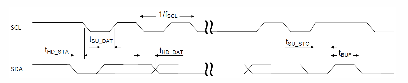
TWI interface electrical specifications
| Symbol | Description | Min. | Typ. | Max. | Units | ||||
|---|---|---|---|---|---|---|---|---|---|
| fTWI,SCL | Bit rates for TWI1 | 100 | 400 | kbps | |||||
| tTWI,START | Time from STARTRX/STARTTX task to transmission started | 1.5 | µs |
Two Wire Interface (TWI) timing specifications
| Symbol | Description | Min. | Typ. | Max. | Units | ||||
|---|---|---|---|---|---|---|---|---|---|
| tTWI,SU_DAT | Data setup time before positive edge on SCL – all modes | 300 | ns | ||||||
| tTWI,HD_DAT | Data hold time after negative edge on SCL – all modes | 500 | ns | ||||||
| tTWI,HD_STA,100kbps | TWI master hold time for START and repeated START condition, 100 kbps | 10000 | ns | ||||||
| tTWI,HD_STA,250kbps | TWI master hold time for START and repeated START condition, 250kbps | 4000 | ns | ||||||
| tTWI,HD_STA,400kbps | TWI master hold time for START and repeated START condition, 400 kbps | 2500 | ns | ||||||
| tTWI,SU_STO,100kbps | TWI master setup time from SCL high to STOP condition, 100 kbps | 5000 | ns | ||||||
| tTWI,SU_STO,250kbps | TWI master setup time from SCL high to STOP condition, 250 kbps | 2000 | ns | ||||||
| tTWI,SU_STO,400kbps | TWI master setup time from SCL high to STOP condition, 400 kbps | 1250 | ns | ||||||
| tTWI,BUF,100kbps | TWI master bus free time between STOP and START conditions, 100 kbps | 5800 | ns | ||||||
| tTWI,BUF,250kbps | TWI master bus free time between STOP and START conditions, 250 kbps | 2700 | ns | ||||||
| tTWI,BUF,400kbps | TWI master bus free time between STOP and START conditions, 400 kbps | 2100 | ns |