GPIO — General purpose input/output
The general purpose input/output pins (GPIOs) are grouped as one or more ports, with each port having up to 32 GPIOs.
The number of ports and GPIOs per port might vary with product variant and package. Refer to Registers and Pin assignments for more information about the number of GPIOs that are supported.
GPIO has the following user-configurable features:
- Up to 32 GPIO pins per GPIO port
- Configurable output drive strength
- Internal pull-up and pull-down resistors
- Wake-up from high or low level triggers on all pins
- Trigger interrupt on state changes on any pin
- All pins can be used by the PPI task/event system
- One or more GPIO outputs can be controlled through the PPI and GPIOTE channels
- Any pin can be mapped to a peripheral for layout flexibility
- GPIO state changes captured on the SENSE signal can be stored by the LATCH register
The GPIO port peripheral implements up to 32 pins, PIN0 through
PIN31. Each of these pins can be individually configured in the PIN_CNF[n]
registers (n=0..31).
The following parameters can be configured through these registers:
- Direction
- Drive strength
- Enabling of pull-up and pull-down resistors
- Pin sensing
- Input buffer disconnect
- Analog input (for selected pins)
The PIN_CNF registers are retained registers. See POWER — Power supply chapter for more information about retained registers.
Pin configuration
Pins can be individually configured through the SENSE field in the PIN_CNF[n] register to detect either a high or low level input.
When the correct level is detected on a configured pin, the sense mechanism will set the DETECT signal high. Each pin has a separate DETECT signal. Default behavior, defined by the DETECTMODE register, combines all DETECT signals from the pins in the GPIO port into one common DETECT signal and routes it through the system to be utilized by other peripherals. This mechanism is functional in both System ON and System OFF mode. See GPIO port and the GPIO pin details.
The following figure illustrates the GPIO port containing 32 individual pins, where
PIN0 is shown in more detail for reference. All signals on the left side of the
illustration are used by other peripherals in the system and therefore not directly available to
the CPU.
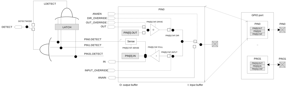
Pins should be in a level that cannot trigger the sense mechanism before being enabled. If the SENSE condition configured in the PIN_CNF registers is met when the sense mechanism is enabled, the DETECT signal will immediately go high. A PORT event is triggered if the DETECT signal was low before enabling the sense mechanism. See GPIOTE — GPIO tasks and events.
See the following peripherals for more information about how the DETECT signal is used:
- POWER — Power supply - uses the DETECT signal to exit from System OFF mode.
- GPIOTE — GPIO tasks and events - uses the DETECT signal to generate the PORT event.
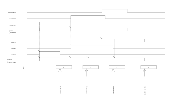
When a pin's PINx.DETECT signal goes high, a flag is set in the LATCH register. For example, when the PIN0.DETECT signal goes high, bit 0 in the LATCH register is set to '1'. If the CPU performs a clear operation on a bit in the LATCH register when the associated PINx.DETECT signal is high, the bit in the LATCH register will not be cleared. The LATCH register will only be cleared if the CPU explicitly clears it by writing a '1' to the bit that shall be cleared, i.e. the LATCH register will not be affected by a PINx.DETECT signal being set low.
The LDETECT signal will be set high when one or more bits in the LATCH register are '1'. The LDETECT signal will be set low when all bits in the LATCH register are successfully cleared to '0'.
If one or more bits in the LATCH register are '1' after the CPU has performed a clear operation on the LATCH register, a rising edge will be generated on the LDETECT signal. This is illustrated in DETECT signal behavior.
The LDETECT signal is by default not connected to the GPIO port's DETECT signal, but via the DETECTMODE register. It is possible to change from default behavior to the DETECT signal that is derived directly from the LDETECT signal. See GPIO port and the GPIO pin details. The following figure illustrates the DETECT signal behavior for these two alternatives.
The input buffer of a GPIO pin can be disconnected from the pin to enable power savings when the pin is not used as an input, see GPIO port and the GPIO pin details. Input buffers must be connected to get a valid input value in the IN register, and for the sense mechanism to get access to the pin.
Other peripherals in the system can connect to GPIO pins and override their output value and configuration, or read their analog or digital input value. See GPIO port and the GPIO pin details.
Selected pins also support analog input signals, see ANAIN in GPIO port and the GPIO pin details. The assignment of the analog pins can be found in Pin assignments.
Registers
| Base address | Peripheral | Instance | Description | Configuration | |
|---|---|---|---|---|---|
| 0x50000000 | GPIO | P0 | General purpose input and output | ||
| Register | Offset | Description | |
|---|---|---|---|
| OUT | 0x504 | Write GPIO port | |
| OUTSET | 0x508 | Set individual bits in GPIO port | |
| OUTCLR | 0x50C | Clear individual bits in GPIO port | |
| IN | 0x510 | Read GPIO port | |
| DIR | 0x514 | Direction of GPIO pins | |
| DIRSET | 0x518 | DIR set register | |
| DIRCLR | 0x51C | DIR clear register | |
| LATCH | 0x520 | Latch register indicating what GPIO pins that have met the criteria set in the PIN_CNF[n].SENSE registers | |
| DETECTMODE | 0x524 | Select between default DETECT signal behaviour and LDETECT mode | |
| PIN_CNF[0] | 0x700 | Configuration of GPIO pins | |
| PIN_CNF[1] | 0x704 | Configuration of GPIO pins | |
| PIN_CNF[2] | 0x708 | Configuration of GPIO pins | |
| PIN_CNF[3] | 0x70C | Configuration of GPIO pins | |
| PIN_CNF[4] | 0x710 | Configuration of GPIO pins | |
| PIN_CNF[5] | 0x714 | Configuration of GPIO pins | |
| PIN_CNF[6] | 0x718 | Configuration of GPIO pins | |
| PIN_CNF[7] | 0x71C | Configuration of GPIO pins | |
| PIN_CNF[8] | 0x720 | Configuration of GPIO pins | |
| PIN_CNF[9] | 0x724 | Configuration of GPIO pins | |
| PIN_CNF[10] | 0x728 | Configuration of GPIO pins | |
| PIN_CNF[11] | 0x72C | Configuration of GPIO pins | |
| PIN_CNF[12] | 0x730 | Configuration of GPIO pins | |
| PIN_CNF[13] | 0x734 | Configuration of GPIO pins | |
| PIN_CNF[14] | 0x738 | Configuration of GPIO pins | |
| PIN_CNF[15] | 0x73C | Configuration of GPIO pins | |
| PIN_CNF[16] | 0x740 | Configuration of GPIO pins | |
| PIN_CNF[17] | 0x744 | Configuration of GPIO pins | |
| PIN_CNF[18] | 0x748 | Configuration of GPIO pins | |
| PIN_CNF[19] | 0x74C | Configuration of GPIO pins | |
| PIN_CNF[20] | 0x750 | Configuration of GPIO pins | |
| PIN_CNF[21] | 0x754 | Configuration of GPIO pins | |
| PIN_CNF[22] | 0x758 | Configuration of GPIO pins | |
| PIN_CNF[23] | 0x75C | Configuration of GPIO pins | |
| PIN_CNF[24] | 0x760 | Configuration of GPIO pins | |
| PIN_CNF[25] | 0x764 | Configuration of GPIO pins | |
| PIN_CNF[26] | 0x768 | Configuration of GPIO pins | |
| PIN_CNF[27] | 0x76C | Configuration of GPIO pins | |
| PIN_CNF[28] | 0x770 | Configuration of GPIO pins | |
| PIN_CNF[29] | 0x774 | Configuration of GPIO pins | |
| PIN_CNF[30] | 0x778 | Configuration of GPIO pins | |
| PIN_CNF[31] | 0x77C | Configuration of GPIO pins | |
OUT
Address offset: 0x504
Write GPIO port
| Bit number | 31 | 30 | 29 | 28 | 27 | 26 | 25 | 24 | 23 | 22 | 21 | 20 | 19 | 18 | 17 | 16 | 15 | 14 | 13 | 12 | 11 | 10 | 9 | 8 | 7 | 6 | 5 | 4 | 3 | 2 | 1 | 0 | |||
|---|---|---|---|---|---|---|---|---|---|---|---|---|---|---|---|---|---|---|---|---|---|---|---|---|---|---|---|---|---|---|---|---|---|---|---|
| ID | f | e | d | c | b | a | Z | Y | X | W | V | U | T | S | R | Q | P | O | N | M | L | K | J | I | H | G | F | E | D | C | B | A | |||
| Reset 0x00000000 | 0 | 0 | 0 | 0 | 0 | 0 | 0 | 0 | 0 | 0 | 0 | 0 | 0 | 0 | 0 | 0 | 0 | 0 | 0 | 0 | 0 | 0 | 0 | 0 | 0 | 0 | 0 | 0 | 0 | 0 | 0 | 0 | |||
| ID | Access | Field | Value ID | Value | Description | ||||||||||||||||||||||||||||||
| A-f | RW | PIN[i] (i=0..31) | Pin i | ||||||||||||||||||||||||||||||||
Low | 0 | Pin driver is low | |||||||||||||||||||||||||||||||||
High | 1 | Pin driver is high | |||||||||||||||||||||||||||||||||
OUTSET
Address offset: 0x508
Set individual bits in GPIO port
Read: reads value of OUT register.
| Bit number | 31 | 30 | 29 | 28 | 27 | 26 | 25 | 24 | 23 | 22 | 21 | 20 | 19 | 18 | 17 | 16 | 15 | 14 | 13 | 12 | 11 | 10 | 9 | 8 | 7 | 6 | 5 | 4 | 3 | 2 | 1 | 0 | |||
|---|---|---|---|---|---|---|---|---|---|---|---|---|---|---|---|---|---|---|---|---|---|---|---|---|---|---|---|---|---|---|---|---|---|---|---|
| ID | f | e | d | c | b | a | Z | Y | X | W | V | U | T | S | R | Q | P | O | N | M | L | K | J | I | H | G | F | E | D | C | B | A | |||
| Reset 0x00000000 | 0 | 0 | 0 | 0 | 0 | 0 | 0 | 0 | 0 | 0 | 0 | 0 | 0 | 0 | 0 | 0 | 0 | 0 | 0 | 0 | 0 | 0 | 0 | 0 | 0 | 0 | 0 | 0 | 0 | 0 | 0 | 0 | |||
| ID | Access | Field | Value ID | Value | Description | ||||||||||||||||||||||||||||||
| A-f | RW | PIN[i] (i=0..31) | Pin i | ||||||||||||||||||||||||||||||||
Low | 0 | Read: pin driver is low | |||||||||||||||||||||||||||||||||
High | 1 | Read: pin driver is high | |||||||||||||||||||||||||||||||||
Set | 1 | Write: writing a '1' sets the pin high; writing a '0' has no effect | |||||||||||||||||||||||||||||||||
OUTCLR
Address offset: 0x50C
Clear individual bits in GPIO port
Read: reads value of OUT register.
| Bit number | 31 | 30 | 29 | 28 | 27 | 26 | 25 | 24 | 23 | 22 | 21 | 20 | 19 | 18 | 17 | 16 | 15 | 14 | 13 | 12 | 11 | 10 | 9 | 8 | 7 | 6 | 5 | 4 | 3 | 2 | 1 | 0 | |||
|---|---|---|---|---|---|---|---|---|---|---|---|---|---|---|---|---|---|---|---|---|---|---|---|---|---|---|---|---|---|---|---|---|---|---|---|
| ID | f | e | d | c | b | a | Z | Y | X | W | V | U | T | S | R | Q | P | O | N | M | L | K | J | I | H | G | F | E | D | C | B | A | |||
| Reset 0x00000000 | 0 | 0 | 0 | 0 | 0 | 0 | 0 | 0 | 0 | 0 | 0 | 0 | 0 | 0 | 0 | 0 | 0 | 0 | 0 | 0 | 0 | 0 | 0 | 0 | 0 | 0 | 0 | 0 | 0 | 0 | 0 | 0 | |||
| ID | Access | Field | Value ID | Value | Description | ||||||||||||||||||||||||||||||
| A-f | RW | PIN[i] (i=0..31) | Pin i | ||||||||||||||||||||||||||||||||
Low | 0 | Read: pin driver is low | |||||||||||||||||||||||||||||||||
High | 1 | Read: pin driver is high | |||||||||||||||||||||||||||||||||
Clear | 1 | Write: writing a '1' sets the pin low; writing a '0' has no effect | |||||||||||||||||||||||||||||||||
IN
Address offset: 0x510
Read GPIO port
| Bit number | 31 | 30 | 29 | 28 | 27 | 26 | 25 | 24 | 23 | 22 | 21 | 20 | 19 | 18 | 17 | 16 | 15 | 14 | 13 | 12 | 11 | 10 | 9 | 8 | 7 | 6 | 5 | 4 | 3 | 2 | 1 | 0 | |||
|---|---|---|---|---|---|---|---|---|---|---|---|---|---|---|---|---|---|---|---|---|---|---|---|---|---|---|---|---|---|---|---|---|---|---|---|
| ID | f | e | d | c | b | a | Z | Y | X | W | V | U | T | S | R | Q | P | O | N | M | L | K | J | I | H | G | F | E | D | C | B | A | |||
| Reset 0x00000000 | 0 | 0 | 0 | 0 | 0 | 0 | 0 | 0 | 0 | 0 | 0 | 0 | 0 | 0 | 0 | 0 | 0 | 0 | 0 | 0 | 0 | 0 | 0 | 0 | 0 | 0 | 0 | 0 | 0 | 0 | 0 | 0 | |||
| ID | Access | Field | Value ID | Value | Description | ||||||||||||||||||||||||||||||
| A-f | R | PIN[i] (i=0..31) | Pin i | ||||||||||||||||||||||||||||||||
Low | 0 | Pin input is low | |||||||||||||||||||||||||||||||||
High | 1 | Pin input is high | |||||||||||||||||||||||||||||||||
DIR
Address offset: 0x514
Direction of GPIO pins
| Bit number | 31 | 30 | 29 | 28 | 27 | 26 | 25 | 24 | 23 | 22 | 21 | 20 | 19 | 18 | 17 | 16 | 15 | 14 | 13 | 12 | 11 | 10 | 9 | 8 | 7 | 6 | 5 | 4 | 3 | 2 | 1 | 0 | |||
|---|---|---|---|---|---|---|---|---|---|---|---|---|---|---|---|---|---|---|---|---|---|---|---|---|---|---|---|---|---|---|---|---|---|---|---|
| ID | f | e | d | c | b | a | Z | Y | X | W | V | U | T | S | R | Q | P | O | N | M | L | K | J | I | H | G | F | E | D | C | B | A | |||
| Reset 0x00000000 | 0 | 0 | 0 | 0 | 0 | 0 | 0 | 0 | 0 | 0 | 0 | 0 | 0 | 0 | 0 | 0 | 0 | 0 | 0 | 0 | 0 | 0 | 0 | 0 | 0 | 0 | 0 | 0 | 0 | 0 | 0 | 0 | |||
| ID | Access | Field | Value ID | Value | Description | ||||||||||||||||||||||||||||||
| A-f | RW | PIN[i] (i=0..31) | Pin i | ||||||||||||||||||||||||||||||||
Input | 0 | Pin set as input | |||||||||||||||||||||||||||||||||
Output | 1 | Pin set as output | |||||||||||||||||||||||||||||||||
DIRSET
Address offset: 0x518
DIR set register
Read: reads value of DIR register.
| Bit number | 31 | 30 | 29 | 28 | 27 | 26 | 25 | 24 | 23 | 22 | 21 | 20 | 19 | 18 | 17 | 16 | 15 | 14 | 13 | 12 | 11 | 10 | 9 | 8 | 7 | 6 | 5 | 4 | 3 | 2 | 1 | 0 | |||
|---|---|---|---|---|---|---|---|---|---|---|---|---|---|---|---|---|---|---|---|---|---|---|---|---|---|---|---|---|---|---|---|---|---|---|---|
| ID | f | e | d | c | b | a | Z | Y | X | W | V | U | T | S | R | Q | P | O | N | M | L | K | J | I | H | G | F | E | D | C | B | A | |||
| Reset 0x00000000 | 0 | 0 | 0 | 0 | 0 | 0 | 0 | 0 | 0 | 0 | 0 | 0 | 0 | 0 | 0 | 0 | 0 | 0 | 0 | 0 | 0 | 0 | 0 | 0 | 0 | 0 | 0 | 0 | 0 | 0 | 0 | 0 | |||
| ID | Access | Field | Value ID | Value | Description | ||||||||||||||||||||||||||||||
| A-f | RW | PIN[i] (i=0..31) | Set as output pin i | ||||||||||||||||||||||||||||||||
Input | 0 | Read: pin set as input | |||||||||||||||||||||||||||||||||
Output | 1 | Read: pin set as output | |||||||||||||||||||||||||||||||||
Set | 1 | Write: writing a '1' sets pin to output; writing a '0' has no effect | |||||||||||||||||||||||||||||||||
DIRCLR
Address offset: 0x51C
DIR clear register
Read: reads value of DIR register.
| Bit number | 31 | 30 | 29 | 28 | 27 | 26 | 25 | 24 | 23 | 22 | 21 | 20 | 19 | 18 | 17 | 16 | 15 | 14 | 13 | 12 | 11 | 10 | 9 | 8 | 7 | 6 | 5 | 4 | 3 | 2 | 1 | 0 | |||
|---|---|---|---|---|---|---|---|---|---|---|---|---|---|---|---|---|---|---|---|---|---|---|---|---|---|---|---|---|---|---|---|---|---|---|---|
| ID | f | e | d | c | b | a | Z | Y | X | W | V | U | T | S | R | Q | P | O | N | M | L | K | J | I | H | G | F | E | D | C | B | A | |||
| Reset 0x00000000 | 0 | 0 | 0 | 0 | 0 | 0 | 0 | 0 | 0 | 0 | 0 | 0 | 0 | 0 | 0 | 0 | 0 | 0 | 0 | 0 | 0 | 0 | 0 | 0 | 0 | 0 | 0 | 0 | 0 | 0 | 0 | 0 | |||
| ID | Access | Field | Value ID | Value | Description | ||||||||||||||||||||||||||||||
| A-f | RW | PIN[i] (i=0..31) | Set as input pin i | ||||||||||||||||||||||||||||||||
Input | 0 | Read: pin set as input | |||||||||||||||||||||||||||||||||
Output | 1 | Read: pin set as output | |||||||||||||||||||||||||||||||||
Clear | 1 | Write: writing a '1' sets pin to input; writing a '0' has no effect | |||||||||||||||||||||||||||||||||
LATCH
Address offset: 0x520
Latch register indicating what GPIO pins that have met the criteria set in the PIN_CNF[n].SENSE registers
| Bit number | 31 | 30 | 29 | 28 | 27 | 26 | 25 | 24 | 23 | 22 | 21 | 20 | 19 | 18 | 17 | 16 | 15 | 14 | 13 | 12 | 11 | 10 | 9 | 8 | 7 | 6 | 5 | 4 | 3 | 2 | 1 | 0 | |||
|---|---|---|---|---|---|---|---|---|---|---|---|---|---|---|---|---|---|---|---|---|---|---|---|---|---|---|---|---|---|---|---|---|---|---|---|
| ID | f | e | d | c | b | a | Z | Y | X | W | V | U | T | S | R | Q | P | O | N | M | L | K | J | I | H | G | F | E | D | C | B | A | |||
| Reset 0x00000000 | 0 | 0 | 0 | 0 | 0 | 0 | 0 | 0 | 0 | 0 | 0 | 0 | 0 | 0 | 0 | 0 | 0 | 0 | 0 | 0 | 0 | 0 | 0 | 0 | 0 | 0 | 0 | 0 | 0 | 0 | 0 | 0 | |||
| ID | Access | Field | Value ID | Value | Description | ||||||||||||||||||||||||||||||
| A-f | RW | PIN[i] (i=0..31) | Status on whether PINi has met criteria set in PIN_CNFi.SENSE register. Write '1' to clear. | ||||||||||||||||||||||||||||||||
NotLatched | 0 | Criteria has not been met | |||||||||||||||||||||||||||||||||
Latched | 1 | Criteria has been met | |||||||||||||||||||||||||||||||||
DETECTMODE
Address offset: 0x524
Select between default DETECT signal behaviour and LDETECT mode
| Bit number | 31 | 30 | 29 | 28 | 27 | 26 | 25 | 24 | 23 | 22 | 21 | 20 | 19 | 18 | 17 | 16 | 15 | 14 | 13 | 12 | 11 | 10 | 9 | 8 | 7 | 6 | 5 | 4 | 3 | 2 | 1 | 0 | |||
|---|---|---|---|---|---|---|---|---|---|---|---|---|---|---|---|---|---|---|---|---|---|---|---|---|---|---|---|---|---|---|---|---|---|---|---|
| ID | A | ||||||||||||||||||||||||||||||||||
| Reset 0x00000000 | 0 | 0 | 0 | 0 | 0 | 0 | 0 | 0 | 0 | 0 | 0 | 0 | 0 | 0 | 0 | 0 | 0 | 0 | 0 | 0 | 0 | 0 | 0 | 0 | 0 | 0 | 0 | 0 | 0 | 0 | 0 | 0 | |||
| ID | Access | Field | Value ID | Value | Description | ||||||||||||||||||||||||||||||
| A | RW | DETECTMODE | Select between default DETECT signal behaviour and LDETECT mode | ||||||||||||||||||||||||||||||||
Default | 0 | DETECT directly connected to PIN DETECT signals | |||||||||||||||||||||||||||||||||
LDETECT | 1 | Use the latched LDETECT behaviour | |||||||||||||||||||||||||||||||||
PIN_CNF[n] (n=0..31)
Address offset: 0x700 + (n × 0x4)
Configuration of GPIO pins
| Bit number | 31 | 30 | 29 | 28 | 27 | 26 | 25 | 24 | 23 | 22 | 21 | 20 | 19 | 18 | 17 | 16 | 15 | 14 | 13 | 12 | 11 | 10 | 9 | 8 | 7 | 6 | 5 | 4 | 3 | 2 | 1 | 0 | |||
|---|---|---|---|---|---|---|---|---|---|---|---|---|---|---|---|---|---|---|---|---|---|---|---|---|---|---|---|---|---|---|---|---|---|---|---|
| ID | E | E | D | D | D | C | C | B | A | ||||||||||||||||||||||||||
| Reset 0x00000002 | 0 | 0 | 0 | 0 | 0 | 0 | 0 | 0 | 0 | 0 | 0 | 0 | 0 | 0 | 0 | 0 | 0 | 0 | 0 | 0 | 0 | 0 | 0 | 0 | 0 | 0 | 0 | 0 | 0 | 0 | 1 | 0 | |||
| ID | Access | Field | Value ID | Value | Description | ||||||||||||||||||||||||||||||
| A | RW | DIR | Pin direction. Same physical register as DIR register | ||||||||||||||||||||||||||||||||
Input | 0 | Configure pin as an input pin | |||||||||||||||||||||||||||||||||
Output | 1 | Configure pin as an output pin | |||||||||||||||||||||||||||||||||
| B | RW | INPUT | Connect or disconnect input buffer | ||||||||||||||||||||||||||||||||
Connect | 0 | Connect input buffer | |||||||||||||||||||||||||||||||||
Disconnect | 1 | Disconnect input buffer | |||||||||||||||||||||||||||||||||
| C | RW | PULL | Pull configuration | ||||||||||||||||||||||||||||||||
Disabled | 0 | No pull | |||||||||||||||||||||||||||||||||
Pulldown | 1 | Pull down on pin | |||||||||||||||||||||||||||||||||
Pullup | 3 | Pull up on pin | |||||||||||||||||||||||||||||||||
| D | RW | DRIVE | Drive configuration | ||||||||||||||||||||||||||||||||
S0S1 | 0 | Standard '0', standard '1' | |||||||||||||||||||||||||||||||||
H0S1 | 1 | High drive '0', standard '1' | |||||||||||||||||||||||||||||||||
S0H1 | 2 | Standard '0', high drive '1' | |||||||||||||||||||||||||||||||||
H0H1 | 3 | High drive '0', high 'drive '1'' | |||||||||||||||||||||||||||||||||
D0S1 | 4 | Disconnect '0' standard '1' (normally used for wired-or connections) | |||||||||||||||||||||||||||||||||
D0H1 | 5 | Disconnect '0', high drive '1' (normally used for wired-or connections) | |||||||||||||||||||||||||||||||||
S0D1 | 6 | Standard '0'. disconnect '1' (normally used for wired-and connections) | |||||||||||||||||||||||||||||||||
H0D1 | 7 | High drive '0', disconnect '1' (normally used for wired-and connections) | |||||||||||||||||||||||||||||||||
| E | RW | SENSE | Pin sensing mechanism | ||||||||||||||||||||||||||||||||
Disabled | 0 | Disabled | |||||||||||||||||||||||||||||||||
High | 2 | Sense for high level | |||||||||||||||||||||||||||||||||
Low | 3 | Sense for low level | |||||||||||||||||||||||||||||||||
Electrical specification
GPIO Electrical Specification
| Symbol | Description | Min. | Typ. | Max. | Units | ||||
|---|---|---|---|---|---|---|---|---|---|
| VIH | Input high voltage | 0.7 x VDD | VDD | V | |||||
| VIL | Input low voltage | VSS | 0.3 x VDD | V | |||||
| VOH,SD | Output high voltage, standard drive, 0.5 mA, VDD ≥ 1.7 | VDD-0.4 | VDD | V | |||||
| VOH,HDH | Output high voltage, high drive, 5 mA, VDD ≥ 2.7 V | VDD-0.4 | VDD | V | |||||
| VOH,HDL | Output high voltage, high drive, 3 mA, VDD ≥ 1.7 V | VDD-0.4 | VDD | V | |||||
| VOL,SD | Output low voltage, standard drive, 0.5 mA, VDD ≥ 1.7 | VSS | VSS+0.4 | V | |||||
| VOL,HDH | Output low voltage, high drive, 5 mA, VDD ≥ 2.7 V | VSS | VSS+0.4 | V | |||||
| VOL,HDL | Output low voltage, high drive, 3 mA, VDD ≥ 1.7 V | VSS | VSS+0.4 | V | |||||
| IOL,SD | Current at VSS+0.4 V, output set low, standard drive, VDD ≥ 1.7 | 1 | 2 | 4 | mA | ||||
| IOL,HDH | Current at VSS+0.4 V, output set low, high drive, VDD ≥ 2.7 V | 6 | 10 | 15 | mA | ||||
| IOL,HDL | Current at VSS+0.4 V, output set low, high drive, VDD ≥ 1.7 V | 3 | mA | ||||||
| IOH,SD | Current at VDD-0.4 V, output set high, standard drive, VDD ≥ 1.7 | 1 | 2 | 4 | mA | ||||
| IOH,HDH | Current at VDD-0.4 V, output set high, high drive, VDD ≥ 2.7 V | 6 | 9 | 14 | mA | ||||
| IOH,HDL | Current at VDD-0.4 V, output set high, high drive, VDD ≥ 1.7 V | 3 | mA | ||||||
| tRF,15pF | Rise/fall time, standard drive mode, 10-90%, 15 pF load1 | 9 | ns | ||||||
| tRF,25pF | Rise/fall time, standard drive mode, 10-90%, 25 pF load1 | 13 | ns | ||||||
| tRF,50pF | Rise/fall time, standard drive mode, 10-90%, 50 pF load1 | 25 | ns | ||||||
| tHRF,15pF | Rise/Fall time, high drive mode, 10-90%, 15 pF load1 | 4 | ns | ||||||
| tHRF,25pF | Rise/Fall time, high drive mode, 10-90%, 25 pF load1 | 5 | ns | ||||||
| tHRF,50pF | Rise/Fall time, high drive mode, 10-90%, 50 pF load1 | 8 | ns | ||||||
| RPU | Pull-up resistance | 11 | 13 | 16 | kΩ | ||||
| RPD | Pull-down resistance | 11 | 13 | 16 | kΩ | ||||
| CPAD | Pad capacitance | 3 | pF |