SPI — Serial peripheral interface master
The SPI master provides a simple CPU interface which includes a TXD register for sending data and an RXD register for receiving data. This section is added for legacy support for now.
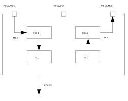
RXD-1 and TXD+1 illustrate the double buffered version of RXD and TXD respectively.
Functional description
The TXD and RXD registers are double-buffered to enable some degree of uninterrupted data flow in and out of the SPI master.
The SPI master does not implement support for chip select directly. Therefore, the CPU must use available GPIOs to select the correct slave and control this independently of the SPI master. The SPI master supports SPI modes 0 through 3.
| Mode | Clock polarity | Clock phase |
|---|---|---|
| CPOL | CPHA | |
| SPI_MODE0 | 0 (Leading) | 0 (Active high) |
| SPI_MODE1 | 0 (Leading) | 1 (Active low) |
| SPI_MODE2 | 1 (Trailing) | 0 (Active high) |
| SPI_MODE3 | 1 (Trailing) | 1 (Active low) |
SPI master mode pin configuration
The different signals SCK, MOSI, and MISO associated with the SPI master are mapped to physical pins.
This mapping is according to the configuration specified in the PSEL.SCK, PSEL.MOSI, and PSEL.MISO registers respectively. If the CONNECT field of a PSEL.xxx register is set to Disconnected, the associated SPI master signal is not connected to any physical pin. The PSEL.SCK, PSEL.MOSI, and PSEL.MISO registers and their configurations are only used as long as the SPI master is enabled, and retained only as long as the device is in ON mode. PSEL.SCK, PSEL.MOSI, and PSEL.MISO must only be configured when the SPI master is disabled.
To secure correct behavior in the SPI, the pins used by the SPI must be configured in the GPIO peripheral as described in GPIO configuration prior to enabling the SPI. The SCK must always be connected to a pin, and that pin's input buffer must always be connected for the SPI to work. This configuration must be retained in the GPIO for the selected IOs as long as the SPI is enabled.
Only one peripheral can be assigned to drive a particular GPIO pin at a time, failing to do so may result in unpredictable behavior.
| SPI master signal | SPI master pin | Direction | Output value |
|---|---|---|---|
| SCK | As specified in PSEL.SCK | Output | Same as CONFIG.CPOL |
| MOSI | As specified in PSEL.MOSI | Output | 0 |
| MISO | As specified in PSEL.MISO | Input | Not applicable |
Shared resources
The SPI shares registers and other resources with other peripherals that have the same ID as the SPI. Therefore, the user must disable all peripherals that have the same ID as the SPI before the SPI can be configured and used.
Disabling a peripheral that has the same ID as the SPI will not reset any of the registers that are shared with the SPI. It is therefore important to configure all relevant SPI registers explicitly to secure that it operates correctly.
See the Instantiation table in Instantiation for details on peripherals and their IDs.
SPI master transaction sequence
An SPI master transaction is started by writing the first byte, which is to be transmitted by the SPI master, to the TXD register.
Since the transmitter is double buffered, the second byte can be written to the TXD register immediately after the first one. The SPI master will then send these bytes in the order they are written to the TXD register.
The SPI master is a synchronous interface, and for every byte that is sent, a different byte will be received at the same time; this is illustrated in SPI master transaction. Bytes that are received will be moved to the RXD register where the CPU can extract them by reading the register. The RXD register is double buffered in the same way as the TXD register, and a second byte can therefore be received at the same time as the first byte is being extracted from RXD by the CPU. The SPI master will generate a READY event every time a new byte is moved to the RXD register. The double buffered byte will be moved from RXD-1 to RXD as soon as the first byte is extracted from RXD. The SPI master will stop when there are no more bytes to send in TXD and TXD+1.
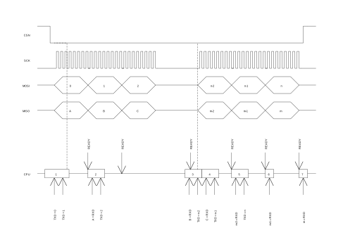
The READY event of the third byte transaction is delayed until B is extracted from RXD in occurrence number 3 on the horizontal lifeline. The reason for this is that the third event is generated first when C is moved from RXD-1 to RXD after B is read.
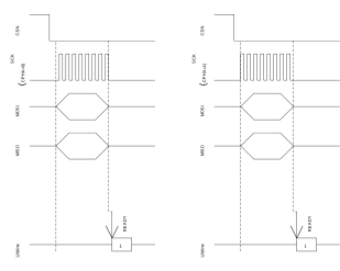
The SPI master will move the incoming byte to the RXD register after a short delay following the SCK clock period of the last bit in the byte. This also means that the READY event will be delayed accordingly, see SPI master transaction. Therefore, it is important that you always clear the READY event, even if the RXD register and the data that is being received is not used.
Registers
| Base address | Peripheral | Instance | Description | Configuration | |
|---|---|---|---|---|---|
| 0x40004000 | SPI | SPI0 | SPI master | Deprecated | |
| Register | Offset | Description | |
|---|---|---|---|
| EVENTS_READY | 0x108 | TXD byte sent and RXD byte received | |
| INTENSET | 0x304 | Enable interrupt | |
| INTENCLR | 0x308 | Disable interrupt | |
| ENABLE | 0x500 | Enable SPI | |
| PSEL.SCK | 0x508 | Pin select for SCK | |
| PSEL.MOSI | 0x50C | Pin select for MOSI signal | |
| PSEL.MISO | 0x510 | Pin select for MISO signal | |
| RXD | 0x518 | RXD register | |
| TXD | 0x51C | TXD register | |
| FREQUENCY | 0x524 | SPI frequency. Accuracy depends on the HFCLK source selected. | |
| CONFIG | 0x554 | Configuration register | |
EVENTS_READY
Address offset: 0x108
TXD byte sent and RXD byte received
| Bit number | 31 | 30 | 29 | 28 | 27 | 26 | 25 | 24 | 23 | 22 | 21 | 20 | 19 | 18 | 17 | 16 | 15 | 14 | 13 | 12 | 11 | 10 | 9 | 8 | 7 | 6 | 5 | 4 | 3 | 2 | 1 | 0 | |||
|---|---|---|---|---|---|---|---|---|---|---|---|---|---|---|---|---|---|---|---|---|---|---|---|---|---|---|---|---|---|---|---|---|---|---|---|
| ID | A | ||||||||||||||||||||||||||||||||||
| Reset 0x00000000 | 0 | 0 | 0 | 0 | 0 | 0 | 0 | 0 | 0 | 0 | 0 | 0 | 0 | 0 | 0 | 0 | 0 | 0 | 0 | 0 | 0 | 0 | 0 | 0 | 0 | 0 | 0 | 0 | 0 | 0 | 0 | 0 | |||
| ID | Access | Field | Value ID | Value | Description | ||||||||||||||||||||||||||||||
| A | RW | EVENTS_READY | TXD byte sent and RXD byte received | ||||||||||||||||||||||||||||||||
NotGenerated | 0 | Event not generated | |||||||||||||||||||||||||||||||||
Generated | 1 | Event generated | |||||||||||||||||||||||||||||||||
INTENSET
Address offset: 0x304
Enable interrupt
| Bit number | 31 | 30 | 29 | 28 | 27 | 26 | 25 | 24 | 23 | 22 | 21 | 20 | 19 | 18 | 17 | 16 | 15 | 14 | 13 | 12 | 11 | 10 | 9 | 8 | 7 | 6 | 5 | 4 | 3 | 2 | 1 | 0 | |||
|---|---|---|---|---|---|---|---|---|---|---|---|---|---|---|---|---|---|---|---|---|---|---|---|---|---|---|---|---|---|---|---|---|---|---|---|
| ID | A | ||||||||||||||||||||||||||||||||||
| Reset 0x00000000 | 0 | 0 | 0 | 0 | 0 | 0 | 0 | 0 | 0 | 0 | 0 | 0 | 0 | 0 | 0 | 0 | 0 | 0 | 0 | 0 | 0 | 0 | 0 | 0 | 0 | 0 | 0 | 0 | 0 | 0 | 0 | 0 | |||
| ID | Access | Field | Value ID | Value | Description | ||||||||||||||||||||||||||||||
| A | RW | READY | Write '1' to enable interrupt for event READY | ||||||||||||||||||||||||||||||||
Set | 1 | Enable | |||||||||||||||||||||||||||||||||
Disabled | 0 | Read: Disabled | |||||||||||||||||||||||||||||||||
Enabled | 1 | Read: Enabled | |||||||||||||||||||||||||||||||||
INTENCLR
Address offset: 0x308
Disable interrupt
| Bit number | 31 | 30 | 29 | 28 | 27 | 26 | 25 | 24 | 23 | 22 | 21 | 20 | 19 | 18 | 17 | 16 | 15 | 14 | 13 | 12 | 11 | 10 | 9 | 8 | 7 | 6 | 5 | 4 | 3 | 2 | 1 | 0 | |||
|---|---|---|---|---|---|---|---|---|---|---|---|---|---|---|---|---|---|---|---|---|---|---|---|---|---|---|---|---|---|---|---|---|---|---|---|
| ID | A | ||||||||||||||||||||||||||||||||||
| Reset 0x00000000 | 0 | 0 | 0 | 0 | 0 | 0 | 0 | 0 | 0 | 0 | 0 | 0 | 0 | 0 | 0 | 0 | 0 | 0 | 0 | 0 | 0 | 0 | 0 | 0 | 0 | 0 | 0 | 0 | 0 | 0 | 0 | 0 | |||
| ID | Access | Field | Value ID | Value | Description | ||||||||||||||||||||||||||||||
| A | RW | READY | Write '1' to disable interrupt for event READY | ||||||||||||||||||||||||||||||||
Clear | 1 | Disable | |||||||||||||||||||||||||||||||||
Disabled | 0 | Read: Disabled | |||||||||||||||||||||||||||||||||
Enabled | 1 | Read: Enabled | |||||||||||||||||||||||||||||||||
ENABLE
Address offset: 0x500
Enable SPI
| Bit number | 31 | 30 | 29 | 28 | 27 | 26 | 25 | 24 | 23 | 22 | 21 | 20 | 19 | 18 | 17 | 16 | 15 | 14 | 13 | 12 | 11 | 10 | 9 | 8 | 7 | 6 | 5 | 4 | 3 | 2 | 1 | 0 | |||
|---|---|---|---|---|---|---|---|---|---|---|---|---|---|---|---|---|---|---|---|---|---|---|---|---|---|---|---|---|---|---|---|---|---|---|---|
| ID | A | A | A | A | |||||||||||||||||||||||||||||||
| Reset 0x00000000 | 0 | 0 | 0 | 0 | 0 | 0 | 0 | 0 | 0 | 0 | 0 | 0 | 0 | 0 | 0 | 0 | 0 | 0 | 0 | 0 | 0 | 0 | 0 | 0 | 0 | 0 | 0 | 0 | 0 | 0 | 0 | 0 | |||
| ID | Access | Field | Value ID | Value | Description | ||||||||||||||||||||||||||||||
| A | RW | ENABLE | Enable or disable SPI | ||||||||||||||||||||||||||||||||
Disabled | 0 | Disable SPI | |||||||||||||||||||||||||||||||||
Enabled | 1 | Enable SPI | |||||||||||||||||||||||||||||||||
PSEL.SCK
Address offset: 0x508
Pin select for SCK
| Bit number | 31 | 30 | 29 | 28 | 27 | 26 | 25 | 24 | 23 | 22 | 21 | 20 | 19 | 18 | 17 | 16 | 15 | 14 | 13 | 12 | 11 | 10 | 9 | 8 | 7 | 6 | 5 | 4 | 3 | 2 | 1 | 0 | |||
|---|---|---|---|---|---|---|---|---|---|---|---|---|---|---|---|---|---|---|---|---|---|---|---|---|---|---|---|---|---|---|---|---|---|---|---|
| ID | C | A | A | A | A | A | |||||||||||||||||||||||||||||
| Reset 0xFFFFFFFF | 1 | 1 | 1 | 1 | 1 | 1 | 1 | 1 | 1 | 1 | 1 | 1 | 1 | 1 | 1 | 1 | 1 | 1 | 1 | 1 | 1 | 1 | 1 | 1 | 1 | 1 | 1 | 1 | 1 | 1 | 1 | 1 | |||
| ID | Access | Field | Value ID | Value | Description | ||||||||||||||||||||||||||||||
| A | RW | PIN | [0..31] | Pin number | |||||||||||||||||||||||||||||||
| C | RW | CONNECT | Connection | ||||||||||||||||||||||||||||||||
Disconnected | 1 | Disconnect | |||||||||||||||||||||||||||||||||
Connected | 0 | Connect | |||||||||||||||||||||||||||||||||
PSEL.MOSI
Address offset: 0x50C
Pin select for MOSI signal
| Bit number | 31 | 30 | 29 | 28 | 27 | 26 | 25 | 24 | 23 | 22 | 21 | 20 | 19 | 18 | 17 | 16 | 15 | 14 | 13 | 12 | 11 | 10 | 9 | 8 | 7 | 6 | 5 | 4 | 3 | 2 | 1 | 0 | |||
|---|---|---|---|---|---|---|---|---|---|---|---|---|---|---|---|---|---|---|---|---|---|---|---|---|---|---|---|---|---|---|---|---|---|---|---|
| ID | C | A | A | A | A | A | |||||||||||||||||||||||||||||
| Reset 0xFFFFFFFF | 1 | 1 | 1 | 1 | 1 | 1 | 1 | 1 | 1 | 1 | 1 | 1 | 1 | 1 | 1 | 1 | 1 | 1 | 1 | 1 | 1 | 1 | 1 | 1 | 1 | 1 | 1 | 1 | 1 | 1 | 1 | 1 | |||
| ID | Access | Field | Value ID | Value | Description | ||||||||||||||||||||||||||||||
| A | RW | PIN | [0..31] | Pin number | |||||||||||||||||||||||||||||||
| C | RW | CONNECT | Connection | ||||||||||||||||||||||||||||||||
Disconnected | 1 | Disconnect | |||||||||||||||||||||||||||||||||
Connected | 0 | Connect | |||||||||||||||||||||||||||||||||
PSEL.MISO
Address offset: 0x510
Pin select for MISO signal
| Bit number | 31 | 30 | 29 | 28 | 27 | 26 | 25 | 24 | 23 | 22 | 21 | 20 | 19 | 18 | 17 | 16 | 15 | 14 | 13 | 12 | 11 | 10 | 9 | 8 | 7 | 6 | 5 | 4 | 3 | 2 | 1 | 0 | |||
|---|---|---|---|---|---|---|---|---|---|---|---|---|---|---|---|---|---|---|---|---|---|---|---|---|---|---|---|---|---|---|---|---|---|---|---|
| ID | C | A | A | A | A | A | |||||||||||||||||||||||||||||
| Reset 0xFFFFFFFF | 1 | 1 | 1 | 1 | 1 | 1 | 1 | 1 | 1 | 1 | 1 | 1 | 1 | 1 | 1 | 1 | 1 | 1 | 1 | 1 | 1 | 1 | 1 | 1 | 1 | 1 | 1 | 1 | 1 | 1 | 1 | 1 | |||
| ID | Access | Field | Value ID | Value | Description | ||||||||||||||||||||||||||||||
| A | RW | PIN | [0..31] | Pin number | |||||||||||||||||||||||||||||||
| C | RW | CONNECT | Connection | ||||||||||||||||||||||||||||||||
Disconnected | 1 | Disconnect | |||||||||||||||||||||||||||||||||
Connected | 0 | Connect | |||||||||||||||||||||||||||||||||
RXD
Address offset: 0x518
RXD register
| Bit number | 31 | 30 | 29 | 28 | 27 | 26 | 25 | 24 | 23 | 22 | 21 | 20 | 19 | 18 | 17 | 16 | 15 | 14 | 13 | 12 | 11 | 10 | 9 | 8 | 7 | 6 | 5 | 4 | 3 | 2 | 1 | 0 | |||
|---|---|---|---|---|---|---|---|---|---|---|---|---|---|---|---|---|---|---|---|---|---|---|---|---|---|---|---|---|---|---|---|---|---|---|---|
| ID | A | A | A | A | A | A | A | A | |||||||||||||||||||||||||||
| Reset 0x00000000 | 0 | 0 | 0 | 0 | 0 | 0 | 0 | 0 | 0 | 0 | 0 | 0 | 0 | 0 | 0 | 0 | 0 | 0 | 0 | 0 | 0 | 0 | 0 | 0 | 0 | 0 | 0 | 0 | 0 | 0 | 0 | 0 | |||
| ID | Access | Field | Value ID | Value | Description | ||||||||||||||||||||||||||||||
| A | R | RXD | RX data received. Double buffered | ||||||||||||||||||||||||||||||||
TXD
Address offset: 0x51C
TXD register
| Bit number | 31 | 30 | 29 | 28 | 27 | 26 | 25 | 24 | 23 | 22 | 21 | 20 | 19 | 18 | 17 | 16 | 15 | 14 | 13 | 12 | 11 | 10 | 9 | 8 | 7 | 6 | 5 | 4 | 3 | 2 | 1 | 0 | |||
|---|---|---|---|---|---|---|---|---|---|---|---|---|---|---|---|---|---|---|---|---|---|---|---|---|---|---|---|---|---|---|---|---|---|---|---|
| ID | A | A | A | A | A | A | A | A | |||||||||||||||||||||||||||
| Reset 0x00000000 | 0 | 0 | 0 | 0 | 0 | 0 | 0 | 0 | 0 | 0 | 0 | 0 | 0 | 0 | 0 | 0 | 0 | 0 | 0 | 0 | 0 | 0 | 0 | 0 | 0 | 0 | 0 | 0 | 0 | 0 | 0 | 0 | |||
| ID | Access | Field | Value ID | Value | Description | ||||||||||||||||||||||||||||||
| A | RW | TXD | TX data to send. Double buffered | ||||||||||||||||||||||||||||||||
FREQUENCY
Address offset: 0x524
SPI frequency. Accuracy depends on the HFCLK source selected.
| Bit number | 31 | 30 | 29 | 28 | 27 | 26 | 25 | 24 | 23 | 22 | 21 | 20 | 19 | 18 | 17 | 16 | 15 | 14 | 13 | 12 | 11 | 10 | 9 | 8 | 7 | 6 | 5 | 4 | 3 | 2 | 1 | 0 | |||
|---|---|---|---|---|---|---|---|---|---|---|---|---|---|---|---|---|---|---|---|---|---|---|---|---|---|---|---|---|---|---|---|---|---|---|---|
| ID | A | A | A | A | A | A | A | A | A | A | A | A | A | A | A | A | A | A | A | A | A | A | A | A | A | A | A | A | A | A | A | A | |||
| Reset 0x04000000 | 0 | 0 | 0 | 0 | 0 | 1 | 0 | 0 | 0 | 0 | 0 | 0 | 0 | 0 | 0 | 0 | 0 | 0 | 0 | 0 | 0 | 0 | 0 | 0 | 0 | 0 | 0 | 0 | 0 | 0 | 0 | 0 | |||
| ID | Access | Field | Value ID | Value | Description | ||||||||||||||||||||||||||||||
| A | RW | FREQUENCY | SPI master data rate | ||||||||||||||||||||||||||||||||
K125 | 0x02000000 | 125 kbps | |||||||||||||||||||||||||||||||||
K250 | 0x04000000 | 250 kbps | |||||||||||||||||||||||||||||||||
K500 | 0x08000000 | 500 kbps | |||||||||||||||||||||||||||||||||
M1 | 0x10000000 | 1 Mbps | |||||||||||||||||||||||||||||||||
M2 | 0x20000000 | 2 Mbps | |||||||||||||||||||||||||||||||||
M4 | 0x40000000 | 4 Mbps | |||||||||||||||||||||||||||||||||
M8 | 0x80000000 | 8 Mbps | |||||||||||||||||||||||||||||||||
CONFIG
Address offset: 0x554
Configuration register
| Bit number | 31 | 30 | 29 | 28 | 27 | 26 | 25 | 24 | 23 | 22 | 21 | 20 | 19 | 18 | 17 | 16 | 15 | 14 | 13 | 12 | 11 | 10 | 9 | 8 | 7 | 6 | 5 | 4 | 3 | 2 | 1 | 0 | |||
|---|---|---|---|---|---|---|---|---|---|---|---|---|---|---|---|---|---|---|---|---|---|---|---|---|---|---|---|---|---|---|---|---|---|---|---|
| ID | C | B | A | ||||||||||||||||||||||||||||||||
| Reset 0x00000000 | 0 | 0 | 0 | 0 | 0 | 0 | 0 | 0 | 0 | 0 | 0 | 0 | 0 | 0 | 0 | 0 | 0 | 0 | 0 | 0 | 0 | 0 | 0 | 0 | 0 | 0 | 0 | 0 | 0 | 0 | 0 | 0 | |||
| ID | Access | Field | Value ID | Value | Description | ||||||||||||||||||||||||||||||
| A | RW | ORDER | Bit order | ||||||||||||||||||||||||||||||||
MsbFirst | 0 | Most significant bit shifted out first | |||||||||||||||||||||||||||||||||
LsbFirst | 1 | Least significant bit shifted out first | |||||||||||||||||||||||||||||||||
| B | RW | CPHA | Serial clock (SCK) phase | ||||||||||||||||||||||||||||||||
Leading | 0 | Sample on leading edge of clock, shift serial data on trailing edge | |||||||||||||||||||||||||||||||||
Trailing | 1 | Sample on trailing edge of clock, shift serial data on leading edge | |||||||||||||||||||||||||||||||||
| C | RW | CPOL | Serial clock (SCK) polarity | ||||||||||||||||||||||||||||||||
ActiveHigh | 0 | Active high | |||||||||||||||||||||||||||||||||
ActiveLow | 1 | Active low | |||||||||||||||||||||||||||||||||
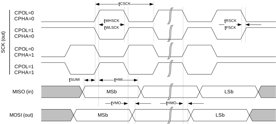
Electrical specification
SPI master interface electrical specifications
Serial Peripheral Interface (SPI) Master timing specifications
| Symbol | Description | Min. | Typ. | Max. | Units | ||||
|---|---|---|---|---|---|---|---|---|---|
| tSPI,CSCK | SCK period | 125 | ns | ||||||
| tSPI,RSCK,LD | SCK rise time, standard drivea | tRF,25pF | |||||||
| tSPI,RSCK,HD | SCK rise time, high drivea | tHRF,25pF | |||||||
| tSPI,FSCK,LD | SCK fall time, standard drivea | tRF,25pF | |||||||
| tSPI,FSCK,HD | SCK fall time, high drivea | tHRF,25pF | |||||||
| tSPI,WHSCK | SCK high timea | (tCSCK/2) – tRSCK | |||||||
| tSPI,WLSCK | SCK low timea | (tCSCK/2) – tFSCK | |||||||
| tSPI,SUMI | MISO to CLK edge setup time | 19 | ns | ||||||
| tSPI,HMI | CLK edge to MISO hold time | 18 | ns | ||||||
| tSPI,VMO | CLK edge to MOSI valid | 59 | ns | ||||||
| tSPI,HMO | MOSI hold time after CLK edge | 20 | ns |