Pin assignments
The pin assignment figures and tables describe the pinouts for the product variants of the chip.
The nRF52810 device provides flexibility when it comes to routing and configuration of the GPIO pins. However, some pins have limitations or recommendations for how the pin should be configured or what it should be used for.
QFN48 pin assignments
The nRF52810 QFN48 pin assignment table and figure describe the pinouts for this variant of the chip.
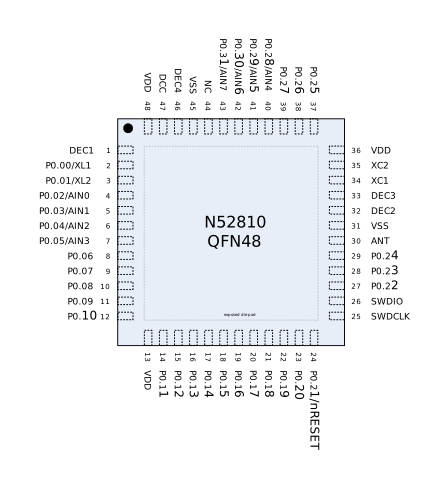
| Pin | Name | Type | Description |
|---|---|---|---|
| 1 | DEC1 | Power | 0.9 V regulator digital supply decoupling |
| 2 | P0.00 XL1 | Digital I/O Analog input | General purpose I/O Connection for 32.768 kHz crystal (LFXO) |
| 3 | P0.01 XL2 | Digital I/O Analog input | General purpose I/O Connection for 32.768 kHz crystal (LFXO) |
| 4 | P0.02 AIN0 | Digital I/O Analog input | General purpose I/O COMP input SAADC input |
| 5 | P0.03 AIN1 | Digital I/O Analog input | General purpose I/O COMP input SAADC input |
| 6 | P0.04 AIN2 | Digital I/O Analog input | General purpose I/O COMP input SAADC input |
| 7 | P0.05 AIN3 | Digital I/O Analog input | General purpose I/O COMP input SAADC input |
| 8 | P0.06 | Digital I/O | General purpose I/O |
| 9 | P0.07 | Digital I/O | General purpose I/O |
| 10 | P0.08 | Digital I/O | General purpose I/O |
11 | P0.09 | Digital I/O | General purpose I/O |
12 | P0.10 | Digital I/O | General purpose I/O |
| 13 | VDD | Power | Power supply |
| 14 | P0.11 | Digital I/O | General purpose I/O |
| 15 | P0.12 | Digital I/O | General purpose I/O |
| 16 | P0.13 | Digital I/O | General purpose I/O |
| 17 | P0.14 | Digital I/O | General purpose I/O |
| 18 | P0.15 | Digital I/O | General purpose I/O |
| 19 | P0.16 | Digital I/O | General purpose I/O |
| 20 | P0.17 | Digital I/O | General purpose I/O |
| 21 | P0.18 | Digital I/O | General purpose I/O |
| 22 | P0.19 | Digital I/O | General purpose I/O |
| 23 | P0.20 | Digital I/O | General purpose I/O |
| 24 | P0.21 nRESET | Digital I/O | General purpose I/O Configurable as pin reset |
| 25 | SWDCLK | Digital input | Serial wire debug clock input for debug and programming |
| 26 | SWDIO | Digital I/O | Serial wire debug I/O for debug and programming |
| 27 | P0.22 | Digital I/O | General purpose I/O |
| 28 | P0.23 | Digital I/O | General purpose I/O |
| 29 | P0.24 | Digital I/O | General purpose I/O |
| 30 | ANT | RF | Single-ended radio antenna connection |
| 31 | VSS | Power | Ground (radio supply) |
| 32 | DEC2 | Power | 1.3 V regulator supply decoupling (radio supply) |
| 33 | DEC3 | Power | Power supply decoupling |
| 34 | XC1 | Analog input | Connection for 32 MHz crystal |
| 35 | XC2 | Analog input | Connection for 32 MHz crystal |
| 36 | VDD | Power | Power supply |
| 37 | P0.25 | Digital I/O | General purpose I/O |
| 38 | P0.26 | Digital I/O | General purpose I/O |
| 39 | P0.27 | Digital I/O | General purpose I/O |
| 40 | P0.28 AIN4 | Digital I/O Analog input | General purpose I/O COMP input SAADC input |
| 41 | P0.29 AIN5 | Digital I/O Analog input | General purpose I/O COMP input SAADC input |
| 42 | P0.30 AIN6 | Digital I/O Analog input | General purpose I/O COMP input SAADC input |
| 43 | P0.31 AIN7 | Digital I/O Analog input | General purpose I/O pin COMP input SAADC input |
| 44 | NC | No connect Leave unconnected | |
| 45 | VSS | Power | Ground |
| 46 | DEC4 | Power | 1.3 V regulator supply decoupling Input from DC/DC regulator Output from 1.3 V LDO |
| 47 | DCC | Power | DC/DC regulator output |
| 48 | VDD | Power | Power supply |
| Die pad | VSS | Power | Ground pad Exposed die pad must be connected to ground (VSS) for proper device operation. |
QFN32 pin assignments
The nRF52810 QFN32 pin assignment table and figure describe the pinouts for this variant of the chip.
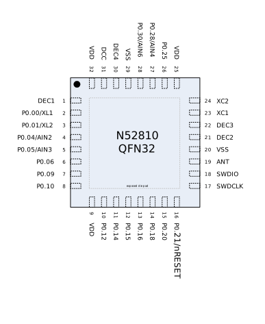
| Pin | Name | Type | Description |
|---|---|---|---|
| 1 | DEC1 | Power | 0.9 V regulator digital supply decoupling |
| 2 | P0.00 XL1 | Digital I/O Analog input | General purpose I/O Connection for 32.768 kHz crystal (LFXO) |
| 3 | P0.01 XL2 | Digital I/O Analog input | General purpose I/O Connection for 32.768 kHz crystal (LFXO) |
| 4 | P0.04 AIN2 | Digital I/O Analog input | General purpose I/O COMP input SAADC input |
| 5 | P0.05 AIN3 | Digital I/O Analog input | General purpose I/O COMP input SAADC input |
| 6 | P0.06 | Digital I/O | General purpose I/O |
| 7 | P0.09 | Digital I/O | General purpose I/O |
| 8 | P0.10 | Digital I/O | General purpose I/O |
| 9 | VDD | Power | Power supply |
| 10 | P0.12 | Digital I/O | General purpose I/O |
| 11 | P0.14 | Digital I/O | General purpose I/O |
| 12 | P0.15 | Digital I/O | General purpose I/O |
| 13 | P0.16 | Digital I/O | General purpose I/O |
| 14 | P0.18 | Digital I/O | General purpose I/O Single wire output |
| 15 | P0.20 | Digital I/O | General purpose I/O |
| 16 | P0.21 nRESET | Digital I/O | General purpose I/O Configurable as pin reset |
| 17 | SWDCLK | Digital input | Serial wire debug clock input for debug and programming |
| 18 | SWDIO | Digital I/O | Serial wire debug I/O for debug and programming |
| 19 | ANT | RF | Single-ended radio antenna connection |
| 20 | VSS | Power | Ground (radio supply) |
| 21 | DEC2 | Power | 1.3 V regulator supply decoupling (radio supply) |
| 22 | DEC3 | Power | Power supply decoupling |
| 23 | XC1 | Analog input | Connection for 32 MHz crystal |
| 24 | XC2 | Analog input | Connection for 32 MHz crystal |
| 25 | VDD | Power | Power supply |
| 26 | P0.25 | Digital I/O | General purpose I/O |
| 27 | P0.28 AIN4 | Digital I/O Analog input | General purpose I/O COMP input SAADC input |
| 28 | P0.30 AIN6 | Digital I/O Analog input | General purpose I/O COMP input SAADC input |
| 29 | VSS | Power | Ground |
| 30 | DEC4 | Power | 1.3 V regulator supply decoupling Input from DC/DC regulator Output from 1.3 V LDO |
| 31 | DCC | Power | DC/DC regulator output |
| 32 | VDD | Power | Power supply |
| Die pad | VSS | Power | Ground pad Exposed die pad must be connected to ground (VSS) for proper device operation. |
WLCSP ball assignments
The nRF52810 ball assignment table and figure describe the assignments for this variant of the chip.
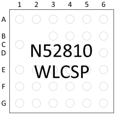
Balls not mentioned in the ball assignments table below are not connected (NC) and must be soldered to the PCB.
| Pin | Name | Type | Description |
|---|---|---|---|
| A1 | XC1 | Analog input | Connection for 32 MHz crystal |
| A2 | XC2 | Analog input | Connection for 32 MHz crystal |
| A3 | DEC2 | Power | 1.3 V regulator supply decoupling (radio supply) |
| A4 | DEC4 | Power | 1.3 V analog supply. Input from DC/DC converter. Output from 1.3 V LDO. |
| A5 | DCC | Power | DC/DC converter output (3.3 V PWM) |
| A6 | VDD | Power | Power (battery) supply |
| B3 | VSS | Power | Ground |
| B4 | VSS | Power | Ground |
| B5 | P0.00 XL1 | Digital I/O Analog input | General purpose I/O Connection for 32.768 kHz crystal (LFXO) |
| B6 | DEC1 | Power | 0.9 V regulator digital supply decoupling |
| C1 | VSS_PA | Power | Ground |
| D3 | VSS | Power | Ground |
| D4 | VSS | Power | Ground |
| D5 | P0.01 XL2 | Digital I/O Analog input | General purpose I/O Connection for 32.768 kHz crystal (LFXO) |
| D6 | P0.03 AIN1 | Digital I/O Analog input | General purpose I/O SAADC/COMP/LPCOMP input |
| E1 | ANT | RF | Single-ended radio antenna connection |
| E2 | P0.18 | Digital I/O | General purpose I/O |
| E3 | VSS | Power | Ground |
| E4 | VSS | Power | Ground |
| E5 | P0.04 AIN2 | Digital I/O Analog input | General purpose I/O SAADC/COMP/LPCOMP input |
| E6 | P0.05 AIN3 | Digital I/O Analog input | General purpose I/O SAADC/COMP/LPCOMP input |
| F1 | SWDIO | Digital I/O | Serial wire debug I/O for debug and programming |
| F2 | P0.21 nRESET | Digital I/O | General purpose I/O Configurable as pin reset |
| F3 | P0.17 | Digital I/O | General purpose I/O |
| F4 | P0.14 | Digital I/O | General purpose I/O |
| F5 | P0.11 | Digital I/O | General purpose I/O |
| F6 | P0.08 | Digital I/O | General purpose I/O |
| G1 | SWDCLK | Digital input | Serial wire debug clock input for debug and programming |
| G2 | P0.20 | Digital I/O | General purpose I/O |
| G3 | P0.16 | Digital I/O | General purpose I/O |
| G4 | P0.15 | Digital I/O | General purpose I/O |
| G5 | P0.12 | Digital I/O | General purpose I/O |
| G6 | VDD | Power | Power (battery) supply |
GPIO pins located near the radio
Radio performance parameters, such as sensitivity, may be affected by high frequency digital I/O with large sink/source current close to the radio power supply and antenna pins.
GPIO recommended usage identifies some GPIO pins that have recommended usage guidelines for maximizing radio performance in an application.
| GPIO | QFN48 pin | QFN32 pin | Recommended usage |
|---|---|---|---|
| P0.25 | 37 | 26 | Low drive, low frequency I/O only. |
| P0.26 | 38 | ||
| P0.27 | 39 | ||
| P0.28 | 40 | 27 | |
| P0.29 | 41 |