COMP — Comparator
The comparator (COMP) compares an input voltage (VIN+) against a second input voltage (VIN-). VIN+ can be derived either from an analog input pin (AIN0-AIN6) or VDD/2. VIN- can be derived from multiple sources depending on the operation mode of the comparator.
Main features of the comparator are:
- Input range from 0 V to VDD
- Single-ended mode
- Fully flexible hysteresis using a 64-level reference ladder
- Differential mode
- Configurable hysteresis
- Reference inputs (VREF):
- VDD
- External reference from AIN0 to AIN7 (between 0 V and VDD)
- Internal references 1.2 V, 1.8 V and 2.4 V
- Three speed/power consumption modes: low-power, normal and high-speed
- Event generation on output changes
- UP event on VIN- > VIN+
- DOWN event on VIN- < VIN+
- CROSS event on VIN+ and VIN- crossing
- READY event on core and internal reference (if used) ready
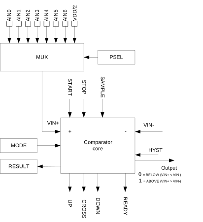
Once enabled (using the ENABLE register), the comparator is started by triggering the START task and stopped by triggering the STOP task. After a start-up time of tCOMP,START, the comparator will generate a READY event to indicate that it is ready for use and that its output is correct. When the COMP module is started, events will be generated every time VIN+ crosses VIN-.
Operation modes
The comparator can be configured to operate in two main operation modes, differential mode and single-ended mode. See the MODE register for more information. In both operation modes, the comparator can operate in different speed and power consumption modes (low-power, normal and high-speed). High-speed mode will consume more power compared to low-power mode, and low-power mode will result in slower response time compared to high-speed mode.
Use the PSEL register to select any of the AIN0-AIN6 pins (or VDD/2) as VIN+ input, irregardless of the operation mode selected for the comparator. The source of VIN- depends on which operation mode is used:
- Differential mode: Derived directly from AIN0 to AIN7
- Single-ended mode: Derived from VREF. VREF can be derived from VDD, AIN0-AIN7 or internal 1.2 V, 1.8 V and 2.4 V references.
The selected analog pins will be acquired by the comparator once it is enabled.
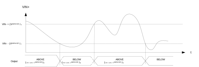
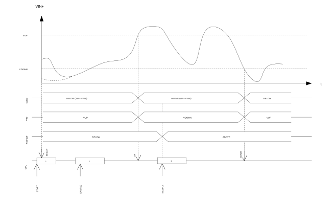
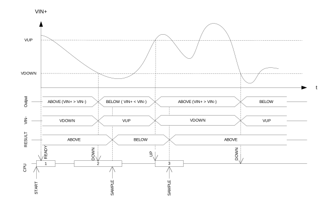
An optional hysteresis on VIN+ and VIN- can be enabled when the module is used in differential mode through the HYST register. In single-ended mode, VUP and VDOWN thresholds can be set to implement a hysteresis using the reference ladder (see Comparator in single-ended mode ). This hysteresis is in the order of magnitude of 30 mV, and shall prevent noise on the signal to create unwanted events. See Hysteresis example where VIN+ starts below VUP for illustration of the effect of an active hysteresis on a noisy input signal.
An upward crossing will generate an UP event and a downward crossing will generate a DOWN event. The CROSS event will be generated every time there is a crossing, independent of direction.
The immediate value of the comparator can be sampled to RESULT register by triggering the SAMPLE task.
Differential mode
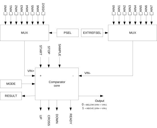
In differential mode, the reference input VIN- is derived directly from one of the AINx pins.
Before enabling the comparator via the ENABLE register, the following registers must be configured for the differential mode:
When HYST register is turned on while in this mode, the output of the comparator (and associated events) will change from ABOVE to BELOW whenever VIN+ becomes lower than VIN- - (VDIFFHYST / 2). It will also change from BELOW to ABOVE whenever VIN+ becomes higher than VIN- + (VDIFFHYST / 2). This behavior is illustrated in Hysteresis enabled in differential mode.
Single-ended mode
In single-ended mode, VIN- is derived from the reference ladder.
Before enabling the comparator via the ENABLE register, the following registers must be configured for the single-ended mode:
The reference ladder uses the reference voltage (VREF) to derive two new voltage references, VUP and VDOWN. VUP and VDOWN are configured using THUP and THDOWN respectively in the TH register. VREF can be derived from any of the available reference sources, configured using the EXTREFSEL and REFSEL registers as illustrated in Comparator in single-ended mode . When AREF is selected in the REFSEL register, the EXTREFSEL register is used to select one of the AIN0-AIN7 analog input pins as reference input. The selected analog pins will be acquired by the comparator once it is enabled.
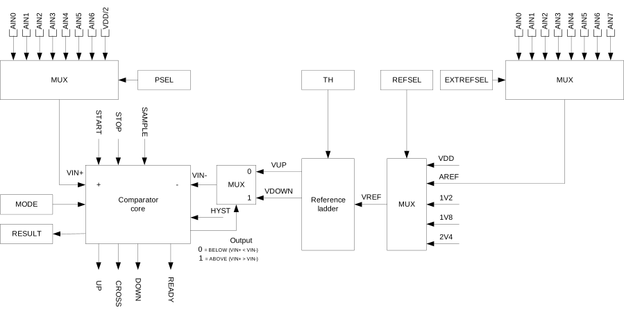
When the comparator core detects that VIN+ > VIN-, i.e. ABOVE as per the RESULT register, VIN- will switch to VDOWN. When VIN+ falls below VIN- again, VIN- will be switched back to VUP. By specifying VUP larger than VDOWN, a hysteresis can be generated as illustrated in Hysteresis example where VIN+ starts below VUP and Hysteresis example where VIN+ starts above VUP.
Writing to HYST has no effect in single-ended mode, and the content of this register is ignored.
Registers
| Base address | Peripheral | Instance | Description | Configuration | |
|---|---|---|---|---|---|
| 0x40013000 | COMP | COMP | General purpose comparator | ||
| Register | Offset | Description | |
|---|---|---|---|
| TASKS_START | 0x000 | Start comparator | |
| TASKS_STOP | 0x004 | Stop comparator | |
| TASKS_SAMPLE | 0x008 | Sample comparator value | |
| EVENTS_READY | 0x100 | COMP is ready and output is valid | |
| EVENTS_DOWN | 0x104 | Downward crossing | |
| EVENTS_UP | 0x108 | Upward crossing | |
| EVENTS_CROSS | 0x10C | Downward or upward crossing | |
| SHORTS | 0x200 | Shortcuts between local events and tasks | |
| INTEN | 0x300 | Enable or disable interrupt | |
| INTENSET | 0x304 | Enable interrupt | |
| INTENCLR | 0x308 | Disable interrupt | |
| RESULT | 0x400 | Compare result | |
| ENABLE | 0x500 | COMP enable | |
| PSEL | 0x504 | Pin select | |
| REFSEL | 0x508 | Reference source select for single-ended mode | |
| EXTREFSEL | 0x50C | External reference select | |
| TH | 0x530 | Threshold configuration for hysteresis unit | |
| MODE | 0x534 | Mode configuration | |
| HYST | 0x538 | Comparator hysteresis enable | |
TASKS_START
Address offset: 0x000
Start comparator
| Bit number | 31 | 30 | 29 | 28 | 27 | 26 | 25 | 24 | 23 | 22 | 21 | 20 | 19 | 18 | 17 | 16 | 15 | 14 | 13 | 12 | 11 | 10 | 9 | 8 | 7 | 6 | 5 | 4 | 3 | 2 | 1 | 0 | |||
|---|---|---|---|---|---|---|---|---|---|---|---|---|---|---|---|---|---|---|---|---|---|---|---|---|---|---|---|---|---|---|---|---|---|---|---|
| ID | A | ||||||||||||||||||||||||||||||||||
| Reset 0x00000000 | 0 | 0 | 0 | 0 | 0 | 0 | 0 | 0 | 0 | 0 | 0 | 0 | 0 | 0 | 0 | 0 | 0 | 0 | 0 | 0 | 0 | 0 | 0 | 0 | 0 | 0 | 0 | 0 | 0 | 0 | 0 | 0 | |||
| ID | Access | Field | Value ID | Value | Description | ||||||||||||||||||||||||||||||
| A | W | TASKS_START | Start comparator | ||||||||||||||||||||||||||||||||
Trigger | 1 | Trigger task | |||||||||||||||||||||||||||||||||
TASKS_STOP
Address offset: 0x004
Stop comparator
| Bit number | 31 | 30 | 29 | 28 | 27 | 26 | 25 | 24 | 23 | 22 | 21 | 20 | 19 | 18 | 17 | 16 | 15 | 14 | 13 | 12 | 11 | 10 | 9 | 8 | 7 | 6 | 5 | 4 | 3 | 2 | 1 | 0 | |||
|---|---|---|---|---|---|---|---|---|---|---|---|---|---|---|---|---|---|---|---|---|---|---|---|---|---|---|---|---|---|---|---|---|---|---|---|
| ID | A | ||||||||||||||||||||||||||||||||||
| Reset 0x00000000 | 0 | 0 | 0 | 0 | 0 | 0 | 0 | 0 | 0 | 0 | 0 | 0 | 0 | 0 | 0 | 0 | 0 | 0 | 0 | 0 | 0 | 0 | 0 | 0 | 0 | 0 | 0 | 0 | 0 | 0 | 0 | 0 | |||
| ID | Access | Field | Value ID | Value | Description | ||||||||||||||||||||||||||||||
| A | W | TASKS_STOP | Stop comparator | ||||||||||||||||||||||||||||||||
Trigger | 1 | Trigger task | |||||||||||||||||||||||||||||||||
TASKS_SAMPLE
Address offset: 0x008
Sample comparator value
| Bit number | 31 | 30 | 29 | 28 | 27 | 26 | 25 | 24 | 23 | 22 | 21 | 20 | 19 | 18 | 17 | 16 | 15 | 14 | 13 | 12 | 11 | 10 | 9 | 8 | 7 | 6 | 5 | 4 | 3 | 2 | 1 | 0 | |||
|---|---|---|---|---|---|---|---|---|---|---|---|---|---|---|---|---|---|---|---|---|---|---|---|---|---|---|---|---|---|---|---|---|---|---|---|
| ID | A | ||||||||||||||||||||||||||||||||||
| Reset 0x00000000 | 0 | 0 | 0 | 0 | 0 | 0 | 0 | 0 | 0 | 0 | 0 | 0 | 0 | 0 | 0 | 0 | 0 | 0 | 0 | 0 | 0 | 0 | 0 | 0 | 0 | 0 | 0 | 0 | 0 | 0 | 0 | 0 | |||
| ID | Access | Field | Value ID | Value | Description | ||||||||||||||||||||||||||||||
| A | W | TASKS_SAMPLE | Sample comparator value | ||||||||||||||||||||||||||||||||
Trigger | 1 | Trigger task | |||||||||||||||||||||||||||||||||
EVENTS_READY
Address offset: 0x100
COMP is ready and output is valid
| Bit number | 31 | 30 | 29 | 28 | 27 | 26 | 25 | 24 | 23 | 22 | 21 | 20 | 19 | 18 | 17 | 16 | 15 | 14 | 13 | 12 | 11 | 10 | 9 | 8 | 7 | 6 | 5 | 4 | 3 | 2 | 1 | 0 | |||
|---|---|---|---|---|---|---|---|---|---|---|---|---|---|---|---|---|---|---|---|---|---|---|---|---|---|---|---|---|---|---|---|---|---|---|---|
| ID | A | ||||||||||||||||||||||||||||||||||
| Reset 0x00000000 | 0 | 0 | 0 | 0 | 0 | 0 | 0 | 0 | 0 | 0 | 0 | 0 | 0 | 0 | 0 | 0 | 0 | 0 | 0 | 0 | 0 | 0 | 0 | 0 | 0 | 0 | 0 | 0 | 0 | 0 | 0 | 0 | |||
| ID | Access | Field | Value ID | Value | Description | ||||||||||||||||||||||||||||||
| A | RW | EVENTS_READY | COMP is ready and output is valid | ||||||||||||||||||||||||||||||||
NotGenerated | 0 | Event not generated | |||||||||||||||||||||||||||||||||
Generated | 1 | Event generated | |||||||||||||||||||||||||||||||||
EVENTS_DOWN
Address offset: 0x104
Downward crossing
| Bit number | 31 | 30 | 29 | 28 | 27 | 26 | 25 | 24 | 23 | 22 | 21 | 20 | 19 | 18 | 17 | 16 | 15 | 14 | 13 | 12 | 11 | 10 | 9 | 8 | 7 | 6 | 5 | 4 | 3 | 2 | 1 | 0 | |||
|---|---|---|---|---|---|---|---|---|---|---|---|---|---|---|---|---|---|---|---|---|---|---|---|---|---|---|---|---|---|---|---|---|---|---|---|
| ID | A | ||||||||||||||||||||||||||||||||||
| Reset 0x00000000 | 0 | 0 | 0 | 0 | 0 | 0 | 0 | 0 | 0 | 0 | 0 | 0 | 0 | 0 | 0 | 0 | 0 | 0 | 0 | 0 | 0 | 0 | 0 | 0 | 0 | 0 | 0 | 0 | 0 | 0 | 0 | 0 | |||
| ID | Access | Field | Value ID | Value | Description | ||||||||||||||||||||||||||||||
| A | RW | EVENTS_DOWN | Downward crossing | ||||||||||||||||||||||||||||||||
NotGenerated | 0 | Event not generated | |||||||||||||||||||||||||||||||||
Generated | 1 | Event generated | |||||||||||||||||||||||||||||||||
EVENTS_UP
Address offset: 0x108
Upward crossing
| Bit number | 31 | 30 | 29 | 28 | 27 | 26 | 25 | 24 | 23 | 22 | 21 | 20 | 19 | 18 | 17 | 16 | 15 | 14 | 13 | 12 | 11 | 10 | 9 | 8 | 7 | 6 | 5 | 4 | 3 | 2 | 1 | 0 | |||
|---|---|---|---|---|---|---|---|---|---|---|---|---|---|---|---|---|---|---|---|---|---|---|---|---|---|---|---|---|---|---|---|---|---|---|---|
| ID | A | ||||||||||||||||||||||||||||||||||
| Reset 0x00000000 | 0 | 0 | 0 | 0 | 0 | 0 | 0 | 0 | 0 | 0 | 0 | 0 | 0 | 0 | 0 | 0 | 0 | 0 | 0 | 0 | 0 | 0 | 0 | 0 | 0 | 0 | 0 | 0 | 0 | 0 | 0 | 0 | |||
| ID | Access | Field | Value ID | Value | Description | ||||||||||||||||||||||||||||||
| A | RW | EVENTS_UP | Upward crossing | ||||||||||||||||||||||||||||||||
NotGenerated | 0 | Event not generated | |||||||||||||||||||||||||||||||||
Generated | 1 | Event generated | |||||||||||||||||||||||||||||||||
EVENTS_CROSS
Address offset: 0x10C
Downward or upward crossing
| Bit number | 31 | 30 | 29 | 28 | 27 | 26 | 25 | 24 | 23 | 22 | 21 | 20 | 19 | 18 | 17 | 16 | 15 | 14 | 13 | 12 | 11 | 10 | 9 | 8 | 7 | 6 | 5 | 4 | 3 | 2 | 1 | 0 | |||
|---|---|---|---|---|---|---|---|---|---|---|---|---|---|---|---|---|---|---|---|---|---|---|---|---|---|---|---|---|---|---|---|---|---|---|---|
| ID | A | ||||||||||||||||||||||||||||||||||
| Reset 0x00000000 | 0 | 0 | 0 | 0 | 0 | 0 | 0 | 0 | 0 | 0 | 0 | 0 | 0 | 0 | 0 | 0 | 0 | 0 | 0 | 0 | 0 | 0 | 0 | 0 | 0 | 0 | 0 | 0 | 0 | 0 | 0 | 0 | |||
| ID | Access | Field | Value ID | Value | Description | ||||||||||||||||||||||||||||||
| A | RW | EVENTS_CROSS | Downward or upward crossing | ||||||||||||||||||||||||||||||||
NotGenerated | 0 | Event not generated | |||||||||||||||||||||||||||||||||
Generated | 1 | Event generated | |||||||||||||||||||||||||||||||||
SHORTS
Address offset: 0x200
Shortcuts between local events and tasks
| Bit number | 31 | 30 | 29 | 28 | 27 | 26 | 25 | 24 | 23 | 22 | 21 | 20 | 19 | 18 | 17 | 16 | 15 | 14 | 13 | 12 | 11 | 10 | 9 | 8 | 7 | 6 | 5 | 4 | 3 | 2 | 1 | 0 | |||
|---|---|---|---|---|---|---|---|---|---|---|---|---|---|---|---|---|---|---|---|---|---|---|---|---|---|---|---|---|---|---|---|---|---|---|---|
| ID | E | D | C | B | A | ||||||||||||||||||||||||||||||
| Reset 0x00000000 | 0 | 0 | 0 | 0 | 0 | 0 | 0 | 0 | 0 | 0 | 0 | 0 | 0 | 0 | 0 | 0 | 0 | 0 | 0 | 0 | 0 | 0 | 0 | 0 | 0 | 0 | 0 | 0 | 0 | 0 | 0 | 0 | |||
| ID | Access | Field | Value ID | Value | Description | ||||||||||||||||||||||||||||||
| A | RW | READY_SAMPLE | |||||||||||||||||||||||||||||||||
Disabled | 0 | Disable shortcut | |||||||||||||||||||||||||||||||||
Enabled | 1 | Enable shortcut | |||||||||||||||||||||||||||||||||
| B | RW | READY_STOP | |||||||||||||||||||||||||||||||||
Disabled | 0 | Disable shortcut | |||||||||||||||||||||||||||||||||
Enabled | 1 | Enable shortcut | |||||||||||||||||||||||||||||||||
| C | RW | DOWN_STOP | |||||||||||||||||||||||||||||||||
Disabled | 0 | Disable shortcut | |||||||||||||||||||||||||||||||||
Enabled | 1 | Enable shortcut | |||||||||||||||||||||||||||||||||
| D | RW | UP_STOP | |||||||||||||||||||||||||||||||||
Disabled | 0 | Disable shortcut | |||||||||||||||||||||||||||||||||
Enabled | 1 | Enable shortcut | |||||||||||||||||||||||||||||||||
| E | RW | CROSS_STOP | |||||||||||||||||||||||||||||||||
Disabled | 0 | Disable shortcut | |||||||||||||||||||||||||||||||||
Enabled | 1 | Enable shortcut | |||||||||||||||||||||||||||||||||
INTEN
Address offset: 0x300
Enable or disable interrupt
| Bit number | 31 | 30 | 29 | 28 | 27 | 26 | 25 | 24 | 23 | 22 | 21 | 20 | 19 | 18 | 17 | 16 | 15 | 14 | 13 | 12 | 11 | 10 | 9 | 8 | 7 | 6 | 5 | 4 | 3 | 2 | 1 | 0 | |||
|---|---|---|---|---|---|---|---|---|---|---|---|---|---|---|---|---|---|---|---|---|---|---|---|---|---|---|---|---|---|---|---|---|---|---|---|
| ID | D | C | B | A | |||||||||||||||||||||||||||||||
| Reset 0x00000000 | 0 | 0 | 0 | 0 | 0 | 0 | 0 | 0 | 0 | 0 | 0 | 0 | 0 | 0 | 0 | 0 | 0 | 0 | 0 | 0 | 0 | 0 | 0 | 0 | 0 | 0 | 0 | 0 | 0 | 0 | 0 | 0 | |||
| ID | Access | Field | Value ID | Value | Description | ||||||||||||||||||||||||||||||
| A | RW | READY | Enable or disable interrupt for event READY | ||||||||||||||||||||||||||||||||
Disabled | 0 | Disable | |||||||||||||||||||||||||||||||||
Enabled | 1 | Enable | |||||||||||||||||||||||||||||||||
| B | RW | DOWN | Enable or disable interrupt for event DOWN | ||||||||||||||||||||||||||||||||
Disabled | 0 | Disable | |||||||||||||||||||||||||||||||||
Enabled | 1 | Enable | |||||||||||||||||||||||||||||||||
| C | RW | UP | Enable or disable interrupt for event UP | ||||||||||||||||||||||||||||||||
Disabled | 0 | Disable | |||||||||||||||||||||||||||||||||
Enabled | 1 | Enable | |||||||||||||||||||||||||||||||||
| D | RW | CROSS | Enable or disable interrupt for event CROSS | ||||||||||||||||||||||||||||||||
Disabled | 0 | Disable | |||||||||||||||||||||||||||||||||
Enabled | 1 | Enable | |||||||||||||||||||||||||||||||||
INTENSET
Address offset: 0x304
Enable interrupt
| Bit number | 31 | 30 | 29 | 28 | 27 | 26 | 25 | 24 | 23 | 22 | 21 | 20 | 19 | 18 | 17 | 16 | 15 | 14 | 13 | 12 | 11 | 10 | 9 | 8 | 7 | 6 | 5 | 4 | 3 | 2 | 1 | 0 | |||
|---|---|---|---|---|---|---|---|---|---|---|---|---|---|---|---|---|---|---|---|---|---|---|---|---|---|---|---|---|---|---|---|---|---|---|---|
| ID | D | C | B | A | |||||||||||||||||||||||||||||||
| Reset 0x00000000 | 0 | 0 | 0 | 0 | 0 | 0 | 0 | 0 | 0 | 0 | 0 | 0 | 0 | 0 | 0 | 0 | 0 | 0 | 0 | 0 | 0 | 0 | 0 | 0 | 0 | 0 | 0 | 0 | 0 | 0 | 0 | 0 | |||
| ID | Access | Field | Value ID | Value | Description | ||||||||||||||||||||||||||||||
| A | RW | READY | Write '1' to enable interrupt for event READY | ||||||||||||||||||||||||||||||||
Set | 1 | Enable | |||||||||||||||||||||||||||||||||
Disabled | 0 | Read: Disabled | |||||||||||||||||||||||||||||||||
Enabled | 1 | Read: Enabled | |||||||||||||||||||||||||||||||||
| B | RW | DOWN | Write '1' to enable interrupt for event DOWN | ||||||||||||||||||||||||||||||||
Set | 1 | Enable | |||||||||||||||||||||||||||||||||
Disabled | 0 | Read: Disabled | |||||||||||||||||||||||||||||||||
Enabled | 1 | Read: Enabled | |||||||||||||||||||||||||||||||||
| C | RW | UP | Write '1' to enable interrupt for event UP | ||||||||||||||||||||||||||||||||
Set | 1 | Enable | |||||||||||||||||||||||||||||||||
Disabled | 0 | Read: Disabled | |||||||||||||||||||||||||||||||||
Enabled | 1 | Read: Enabled | |||||||||||||||||||||||||||||||||
| D | RW | CROSS | Write '1' to enable interrupt for event CROSS | ||||||||||||||||||||||||||||||||
Set | 1 | Enable | |||||||||||||||||||||||||||||||||
Disabled | 0 | Read: Disabled | |||||||||||||||||||||||||||||||||
Enabled | 1 | Read: Enabled | |||||||||||||||||||||||||||||||||
INTENCLR
Address offset: 0x308
Disable interrupt
| Bit number | 31 | 30 | 29 | 28 | 27 | 26 | 25 | 24 | 23 | 22 | 21 | 20 | 19 | 18 | 17 | 16 | 15 | 14 | 13 | 12 | 11 | 10 | 9 | 8 | 7 | 6 | 5 | 4 | 3 | 2 | 1 | 0 | |||
|---|---|---|---|---|---|---|---|---|---|---|---|---|---|---|---|---|---|---|---|---|---|---|---|---|---|---|---|---|---|---|---|---|---|---|---|
| ID | D | C | B | A | |||||||||||||||||||||||||||||||
| Reset 0x00000000 | 0 | 0 | 0 | 0 | 0 | 0 | 0 | 0 | 0 | 0 | 0 | 0 | 0 | 0 | 0 | 0 | 0 | 0 | 0 | 0 | 0 | 0 | 0 | 0 | 0 | 0 | 0 | 0 | 0 | 0 | 0 | 0 | |||
| ID | Access | Field | Value ID | Value | Description | ||||||||||||||||||||||||||||||
| A | RW | READY | Write '1' to disable interrupt for event READY | ||||||||||||||||||||||||||||||||
Clear | 1 | Disable | |||||||||||||||||||||||||||||||||
Disabled | 0 | Read: Disabled | |||||||||||||||||||||||||||||||||
Enabled | 1 | Read: Enabled | |||||||||||||||||||||||||||||||||
| B | RW | DOWN | Write '1' to disable interrupt for event DOWN | ||||||||||||||||||||||||||||||||
Clear | 1 | Disable | |||||||||||||||||||||||||||||||||
Disabled | 0 | Read: Disabled | |||||||||||||||||||||||||||||||||
Enabled | 1 | Read: Enabled | |||||||||||||||||||||||||||||||||
| C | RW | UP | Write '1' to disable interrupt for event UP | ||||||||||||||||||||||||||||||||
Clear | 1 | Disable | |||||||||||||||||||||||||||||||||
Disabled | 0 | Read: Disabled | |||||||||||||||||||||||||||||||||
Enabled | 1 | Read: Enabled | |||||||||||||||||||||||||||||||||
| D | RW | CROSS | Write '1' to disable interrupt for event CROSS | ||||||||||||||||||||||||||||||||
Clear | 1 | Disable | |||||||||||||||||||||||||||||||||
Disabled | 0 | Read: Disabled | |||||||||||||||||||||||||||||||||
Enabled | 1 | Read: Enabled | |||||||||||||||||||||||||||||||||
RESULT
Address offset: 0x400
Compare result
| Bit number | 31 | 30 | 29 | 28 | 27 | 26 | 25 | 24 | 23 | 22 | 21 | 20 | 19 | 18 | 17 | 16 | 15 | 14 | 13 | 12 | 11 | 10 | 9 | 8 | 7 | 6 | 5 | 4 | 3 | 2 | 1 | 0 | |||
|---|---|---|---|---|---|---|---|---|---|---|---|---|---|---|---|---|---|---|---|---|---|---|---|---|---|---|---|---|---|---|---|---|---|---|---|
| ID | A | ||||||||||||||||||||||||||||||||||
| Reset 0x00000000 | 0 | 0 | 0 | 0 | 0 | 0 | 0 | 0 | 0 | 0 | 0 | 0 | 0 | 0 | 0 | 0 | 0 | 0 | 0 | 0 | 0 | 0 | 0 | 0 | 0 | 0 | 0 | 0 | 0 | 0 | 0 | 0 | |||
| ID | Access | Field | Value ID | Value | Description | ||||||||||||||||||||||||||||||
| A | R | RESULT | Result of last compare. Decision point SAMPLE task. | ||||||||||||||||||||||||||||||||
Below | 0 | Input voltage is below the threshold (VIN+ < VIN-) | |||||||||||||||||||||||||||||||||
Above | 1 | Input voltage is above the threshold (VIN+ > VIN-) | |||||||||||||||||||||||||||||||||
ENABLE
Address offset: 0x500
COMP enable
| Bit number | 31 | 30 | 29 | 28 | 27 | 26 | 25 | 24 | 23 | 22 | 21 | 20 | 19 | 18 | 17 | 16 | 15 | 14 | 13 | 12 | 11 | 10 | 9 | 8 | 7 | 6 | 5 | 4 | 3 | 2 | 1 | 0 | |||
|---|---|---|---|---|---|---|---|---|---|---|---|---|---|---|---|---|---|---|---|---|---|---|---|---|---|---|---|---|---|---|---|---|---|---|---|
| ID | A | A | |||||||||||||||||||||||||||||||||
| Reset 0x00000000 | 0 | 0 | 0 | 0 | 0 | 0 | 0 | 0 | 0 | 0 | 0 | 0 | 0 | 0 | 0 | 0 | 0 | 0 | 0 | 0 | 0 | 0 | 0 | 0 | 0 | 0 | 0 | 0 | 0 | 0 | 0 | 0 | |||
| ID | Access | Field | Value ID | Value | Description | ||||||||||||||||||||||||||||||
| A | RW | ENABLE | Enable or disable COMP | ||||||||||||||||||||||||||||||||
Disabled | 0 | Disable | |||||||||||||||||||||||||||||||||
Enabled | 2 | Enable | |||||||||||||||||||||||||||||||||
PSEL
Address offset: 0x504
Pin select
| Bit number | 31 | 30 | 29 | 28 | 27 | 26 | 25 | 24 | 23 | 22 | 21 | 20 | 19 | 18 | 17 | 16 | 15 | 14 | 13 | 12 | 11 | 10 | 9 | 8 | 7 | 6 | 5 | 4 | 3 | 2 | 1 | 0 | |||
|---|---|---|---|---|---|---|---|---|---|---|---|---|---|---|---|---|---|---|---|---|---|---|---|---|---|---|---|---|---|---|---|---|---|---|---|
| ID | A | A | A | ||||||||||||||||||||||||||||||||
| Reset 0x00000000 | 0 | 0 | 0 | 0 | 0 | 0 | 0 | 0 | 0 | 0 | 0 | 0 | 0 | 0 | 0 | 0 | 0 | 0 | 0 | 0 | 0 | 0 | 0 | 0 | 0 | 0 | 0 | 0 | 0 | 0 | 0 | 0 | |||
| ID | Access | Field | Value ID | Value | Description | ||||||||||||||||||||||||||||||
| A | RW | PSEL | Analog pin select | ||||||||||||||||||||||||||||||||
AnalogInput0 | 0 | AIN0 selected as analog input | |||||||||||||||||||||||||||||||||
AnalogInput1 | 1 | AIN1 selected as analog input | |||||||||||||||||||||||||||||||||
AnalogInput2 | 2 | AIN2 selected as analog input | |||||||||||||||||||||||||||||||||
AnalogInput3 | 3 | AIN3 selected as analog input | |||||||||||||||||||||||||||||||||
AnalogInput4 | 4 | AIN4 selected as analog input | |||||||||||||||||||||||||||||||||
AnalogInput5 | 5 | AIN5 selected as analog input | |||||||||||||||||||||||||||||||||
AnalogInput6 | 6 | AIN6 selected as analog input | |||||||||||||||||||||||||||||||||
VddDiv2 | 7 | VDD/2 selected as analog input | |||||||||||||||||||||||||||||||||
REFSEL
Address offset: 0x508
Reference source select for single-ended mode
| Bit number | 31 | 30 | 29 | 28 | 27 | 26 | 25 | 24 | 23 | 22 | 21 | 20 | 19 | 18 | 17 | 16 | 15 | 14 | 13 | 12 | 11 | 10 | 9 | 8 | 7 | 6 | 5 | 4 | 3 | 2 | 1 | 0 | |||
|---|---|---|---|---|---|---|---|---|---|---|---|---|---|---|---|---|---|---|---|---|---|---|---|---|---|---|---|---|---|---|---|---|---|---|---|
| ID | A | A | A | ||||||||||||||||||||||||||||||||
| Reset 0x00000004 | 0 | 0 | 0 | 0 | 0 | 0 | 0 | 0 | 0 | 0 | 0 | 0 | 0 | 0 | 0 | 0 | 0 | 0 | 0 | 0 | 0 | 0 | 0 | 0 | 0 | 0 | 0 | 0 | 0 | 1 | 0 | 0 | |||
| ID | Access | Field | Value ID | Value | Description | ||||||||||||||||||||||||||||||
| A | RW | REFSEL | Reference select | ||||||||||||||||||||||||||||||||
Int1V2 | 0 | VREF = internal 1.2 V reference (VDD >= 1.7 V) | |||||||||||||||||||||||||||||||||
Int1V8 | 1 | VREF = internal 1.8 V reference (VDD >= VREF + 0.2 V) | |||||||||||||||||||||||||||||||||
Int2V4 | 2 | VREF = internal 2.4 V reference (VDD >= VREF + 0.2 V) | |||||||||||||||||||||||||||||||||
VDD | 4 | VREF = VDD | |||||||||||||||||||||||||||||||||
ARef | 5 | VREF = AREF (VDD >= VREF >= AREFMIN) | |||||||||||||||||||||||||||||||||
EXTREFSEL
Address offset: 0x50C
External reference select
| Bit number | 31 | 30 | 29 | 28 | 27 | 26 | 25 | 24 | 23 | 22 | 21 | 20 | 19 | 18 | 17 | 16 | 15 | 14 | 13 | 12 | 11 | 10 | 9 | 8 | 7 | 6 | 5 | 4 | 3 | 2 | 1 | 0 | |||
|---|---|---|---|---|---|---|---|---|---|---|---|---|---|---|---|---|---|---|---|---|---|---|---|---|---|---|---|---|---|---|---|---|---|---|---|
| ID | A | A | A | ||||||||||||||||||||||||||||||||
| Reset 0x00000000 | 0 | 0 | 0 | 0 | 0 | 0 | 0 | 0 | 0 | 0 | 0 | 0 | 0 | 0 | 0 | 0 | 0 | 0 | 0 | 0 | 0 | 0 | 0 | 0 | 0 | 0 | 0 | 0 | 0 | 0 | 0 | 0 | |||
| ID | Access | Field | Value ID | Value | Description | ||||||||||||||||||||||||||||||
| A | RW | EXTREFSEL | External analog reference select | ||||||||||||||||||||||||||||||||
AnalogReference0 | 0 | Use AIN0 as external analog reference | |||||||||||||||||||||||||||||||||
AnalogReference1 | 1 | Use AIN1 as external analog reference | |||||||||||||||||||||||||||||||||
AnalogReference2 | 2 | Use AIN2 as external analog reference | |||||||||||||||||||||||||||||||||
AnalogReference3 | 3 | Use AIN3 as external analog reference | |||||||||||||||||||||||||||||||||
AnalogReference4 | 4 | Use AIN4 as external analog reference | |||||||||||||||||||||||||||||||||
AnalogReference5 | 5 | Use AIN5 as external analog reference | |||||||||||||||||||||||||||||||||
AnalogReference6 | 6 | Use AIN6 as external analog reference | |||||||||||||||||||||||||||||||||
AnalogReference7 | 7 | Use AIN7 as external analog reference | |||||||||||||||||||||||||||||||||
TH
Address offset: 0x530
Threshold configuration for hysteresis unit
| Bit number | 31 | 30 | 29 | 28 | 27 | 26 | 25 | 24 | 23 | 22 | 21 | 20 | 19 | 18 | 17 | 16 | 15 | 14 | 13 | 12 | 11 | 10 | 9 | 8 | 7 | 6 | 5 | 4 | 3 | 2 | 1 | 0 | |||
|---|---|---|---|---|---|---|---|---|---|---|---|---|---|---|---|---|---|---|---|---|---|---|---|---|---|---|---|---|---|---|---|---|---|---|---|
| ID | B | B | B | B | B | B | A | A | A | A | A | A | |||||||||||||||||||||||
| Reset 0x00000000 | 0 | 0 | 0 | 0 | 0 | 0 | 0 | 0 | 0 | 0 | 0 | 0 | 0 | 0 | 0 | 0 | 0 | 0 | 0 | 0 | 0 | 0 | 0 | 0 | 0 | 0 | 0 | 0 | 0 | 0 | 0 | 0 | |||
| ID | Access | Field | Value ID | Value | Description | ||||||||||||||||||||||||||||||
| A | RW | THDOWN | [63:0] | VDOWN = (THDOWN+1)/64*VREF | |||||||||||||||||||||||||||||||
| B | RW | THUP | [63:0] | VUP = (THUP+1)/64*VREF | |||||||||||||||||||||||||||||||
MODE
Address offset: 0x534
Mode configuration
| Bit number | 31 | 30 | 29 | 28 | 27 | 26 | 25 | 24 | 23 | 22 | 21 | 20 | 19 | 18 | 17 | 16 | 15 | 14 | 13 | 12 | 11 | 10 | 9 | 8 | 7 | 6 | 5 | 4 | 3 | 2 | 1 | 0 | |||
|---|---|---|---|---|---|---|---|---|---|---|---|---|---|---|---|---|---|---|---|---|---|---|---|---|---|---|---|---|---|---|---|---|---|---|---|
| ID | B | A | A | ||||||||||||||||||||||||||||||||
| Reset 0x00000000 | 0 | 0 | 0 | 0 | 0 | 0 | 0 | 0 | 0 | 0 | 0 | 0 | 0 | 0 | 0 | 0 | 0 | 0 | 0 | 0 | 0 | 0 | 0 | 0 | 0 | 0 | 0 | 0 | 0 | 0 | 0 | 0 | |||
| ID | Access | Field | Value ID | Value | Description | ||||||||||||||||||||||||||||||
| A | RW | SP | Speed and power modes | ||||||||||||||||||||||||||||||||
Low | 0 | Low-power mode | |||||||||||||||||||||||||||||||||
Normal | 1 | Normal mode | |||||||||||||||||||||||||||||||||
High | 2 | High-speed mode | |||||||||||||||||||||||||||||||||
| B | RW | MAIN | Main operation modes | ||||||||||||||||||||||||||||||||
SE | 0 | Single-ended mode | |||||||||||||||||||||||||||||||||
Diff | 1 | Differential mode | |||||||||||||||||||||||||||||||||
HYST
Address offset: 0x538
Comparator hysteresis enable
| Bit number | 31 | 30 | 29 | 28 | 27 | 26 | 25 | 24 | 23 | 22 | 21 | 20 | 19 | 18 | 17 | 16 | 15 | 14 | 13 | 12 | 11 | 10 | 9 | 8 | 7 | 6 | 5 | 4 | 3 | 2 | 1 | 0 | |||
|---|---|---|---|---|---|---|---|---|---|---|---|---|---|---|---|---|---|---|---|---|---|---|---|---|---|---|---|---|---|---|---|---|---|---|---|
| ID | A | ||||||||||||||||||||||||||||||||||
| Reset 0x00000000 | 0 | 0 | 0 | 0 | 0 | 0 | 0 | 0 | 0 | 0 | 0 | 0 | 0 | 0 | 0 | 0 | 0 | 0 | 0 | 0 | 0 | 0 | 0 | 0 | 0 | 0 | 0 | 0 | 0 | 0 | 0 | 0 | |||
| ID | Access | Field | Value ID | Value | Description | ||||||||||||||||||||||||||||||
| A | RW | HYST | Comparator hysteresis | ||||||||||||||||||||||||||||||||
NoHyst | 0 | Comparator hysteresis disabled | |||||||||||||||||||||||||||||||||
Hyst50mV | 1 | Comparator hysteresis enabled | |||||||||||||||||||||||||||||||||
Electrical specification
COMP Electrical Specification
| Symbol | Description | Min. | Typ. | Max. | Units | ||||
|---|---|---|---|---|---|---|---|---|---|
| tPROPDLY,LP | Propagation delay, low-power modea | 0.6 | µS | ||||||
| tPROPDLY,N | Propagation delay, normal modea | 0.2 | µS | ||||||
| tPROPDLY,HS | Propagation delay, high-speed modea | 0.1 | µS | ||||||
| VDIFFHYST | Optional hysteresis applied to differential input | 30 | mV | ||||||
| VVDD-VREF | Required difference between VDD and a selected VREF, VDD > VREF | 0.3 | V | ||||||
| tINT_REF,START | Startup time for the internal bandgap reference | 50 | 80 | µS | |||||
| EINT_REF | Internal bandgap reference error | -3 | 3 | % | |||||
| VINPUTOFFSET | Input offset | -10 | 10 | mV | |||||
| tCOMP,START | Startup time for the comparator core | 3 | µS |