SAADC — Successive approximation analog-to-digital converter
The ADC is a differential successive approximation register (SAR) analog-to-digital converter.
Listed here are the main features of SAADC:
- 8/10/12-bit resolution, 14-bit resolution with oversampling
- Up to eight input channels
- One channel per single-ended input and two channels per differential input
- Scan mode can be configured with both single-ended channels and differential channels.
- Full scale input range (0 to VDD)
- Sampling triggered via a task from software or a PPI channel for full flexibility on sample frequency source from low power 32.768kHz RTC or more accurate 1/16MHz Timers
- One-shot conversion mode to sample a single channel
- Scan mode to sample a series of channels in sequence. Sample delay between channels is tack + tconv which may vary between channels according to user configuration of tack.
- Support for direct sample transfer to RAM using EasyDMA
- Interrupts on single sample and full buffer events
- Samples stored as 16-bit 2’s complement values for differential and single-ended sampling
- Continuous sampling without the need of an external timer
- Internal resistor string
- Limit checking on the fly
Overview
The ADC supports up to eight external analog input channels, depending on package variant. It can be operated in a one-shot mode with sampling under software control, or a continuous conversion mode with a programmable sampling rate.
The analog inputs can be configured as eight single-ended inputs, four differential inputs or a combination of these. Each channel can be configured to select AIN0 to AIN7 pins, or the VDD pin. Channels can be sampled individually in one-shot or continuous sampling modes, or, using scan mode, multiple channels can be sampled in sequence. Channels can also be oversampled to improve noise performance.
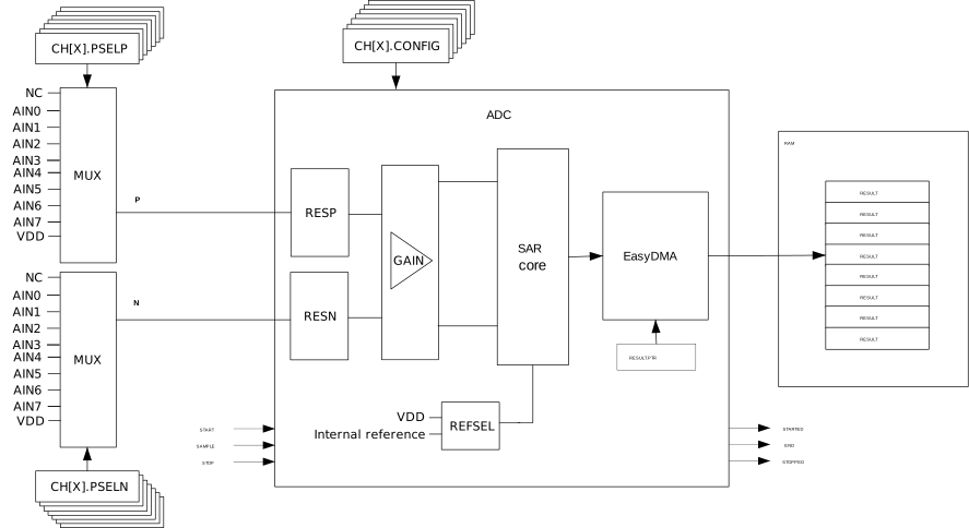
Internally, the ADC is always a differential analog-to-digital converter, but by default it is configured with single-ended input in the MODE field of the CH[n].CONFIG register. In single-ended mode, the negative input will be shorted to ground internally.
The assumption in single-ended mode is that the internal ground of the ADC is the same as the external ground that the measured voltage is referred to. The ADC is thus sensitive to ground bounce on the PCB in single-ended mode. If this is a concern we recommend using differential measurement.
Digital output
The output result of the ADC depends on the settings in the CH[n].CONFIG and RESOLUTION registers as follows:
RESULT = [V(P) – V(N) ] * GAIN/REFERENCE * 2(RESOLUTION - m)where
- V(P)
- is the voltage at input P
- V(N)
- is the voltage at input N
- GAIN
- is the selected gain setting
- REFERENCE
- is the selected reference voltage
and m=0 if CONFIG.MODE=SE, or m=1 if CONFIG.MODE=Diff.
The result generated by the ADC will deviate from the expected due DC errors like offset, gain, differential non-linearity (DNL), and integral non-linearity (INL). See Electrical specification for details on these parameters. The result can also vary due to AC errors like non-linearities in the GAIN block, settling errors due to high source impedance and sampling jitter. For battery measurement the DC errors are most noticeable.
The ADC has a wide selection of gains controlled in the GAIN field of the CH[n].CONFIG register. If CH[n].CONFIG.REFSEL=0, the input range of the ADC core is nominally ±0.6 V differential and the input must be scaled accordingly.
The ADC has a temperature dependent offset. If the ADC is to operate over a large temperature range, we recommend running CALIBRATEOFFSET at regular intervals, a CALIBRATEDONE event will be fired when the calibration is complete
Analog inputs and channels
Up to eight analog input channels, CH[n](n=0..7), can be configured.
See Shared resources for shared input with comparators.
Any one of the available channels can be enabled for the ADC to operate in one-shot mode. If more than one CH[n] is configured, the ADC enters scan mode.
An analog input is selected as a positive converter input if CH[n].PSELP is set, setting CH[n].PSELP also enables the particular channel.
An analog input is selected as a negative converter input if CH[n].PSELN is set. The CH[n].PSELN register will have no effect unless differential mode is enabled, see MODE field in CH[n].CONFIG register.
If more than one of the CH[n].PSELP registers is set, the device enters scan mode. Input selections in scan mode are controlled by the CH[n].PSELP and CH[n].PSELN registers, where CH[n].PSELN is only used if the particular scan channel is specified as differential, see MODE field in CH[n].CONFIG register.
| Channel input | Source | Connectivity |
|---|---|---|
| CH[n].PSELP | AIN0…AIN7 | Yes(any) |
| CH[n].PSELP | VDD | Yes |
| CH[n].PSELN | AIN0…AIN7 | Yes(any) |
| CH[n].PSELN | VDD | Yes |
Operation modes
The ADC input configuration supports one-shot mode, continuous mode and scan mode.
Scan mode and oversampling cannot be combined.
One-shot mode
One-shot operation is configured by enabling only one of the available channels defined by CH[n].PSELP, CH[n].PSELN, and CH[n].CONFIG registers.
Upon a SAMPLE task, the ADC starts to sample the input voltage. The CH[n].CONFIG.TACQ controls the acquisition time.
A DONE event signals that one sample has been taken.
In this mode, the RESULTDONE event has the same meaning as DONE when no oversampling takes place. Note that both events may occur before the actual value has been transferred into RAM by EasyDMA. For more information, see EasyDMA.
Continuous mode
Continuous sampling can be achieved by using the internal timer in the ADC, or triggering the SAMPLE task from one of the general purpose timers through the PPI.
Care shall be taken to ensure that the sample rate fulfils the following criteria, depending on how many channels are active:
fSAMPLE < 1/[tACQ +
tconv]
The SAMPLERATE register can be used as a local timer instead of triggering individual SAMPLE tasks. When SAMPLERATE.MODE is set to Timers, it is sufficient to trigger SAMPLE task only once in order to start the SAADC and triggering the STOP task will stop sampling. The SAMPLERATE.CC field controls the sample rate.
The SAMPLERATE timer mode cannot be combined with SCAN mode, and only one channel can be enabled in this mode.
A DONE event signals that one sample has been taken.
In this mode, the RESULTDONE event has the same meaning as DONE when no oversampling takes place. Note that both events may occur before the actual value has been transferred into RAM by EasyDMA.
Oversampling
An accumulator in the ADC can be used to average noise on the analog input. In general, oversampling improves the signal-to-noise ratio (SNR). Oversampling, however, does not improve the integral non-linearity (INL), or differential non-linearity (DNL).
Oversampling and scan should not be combined, since oversampling and scan will average over input channels.
The accumulator is controlled in the OVERSAMPLE register. The SAMPLE task must be set 2OVERSAMPLE number of times before the result is written to RAM. This can be achieved by:
- Configuring a fixed sampling rate using the local timer or a general purpose timer and PPI to trigger a SAMPLE task
- Triggering SAMPLE 2OVERSAMPLE times from software
- Enabling BURST mode
CH[n].CONFIG.BURST can be enabled to avoid setting SAMPLE task 2OVERSAMPLE times. With BURST = 1 the ADC will sample the input 2OVERSAMPLE times as fast as it can (actual timing: <(tACQ+tCONV)×2OVERSAMPLE). Thus, for the user it will just appear like the conversion took a bit longer time, but other than that, it is similar to one-shot mode. Scan mode can be combined with BURST=1, if burst is enabled on all channels.
A DONE event signals that one sample has been taken.
In this mode, the RESULTDONE event signals that enough conversions have taken place for an oversampled result to get transferred into RAM. Note that both events may occur before the actual value has been transferred into RAM by EasyDMA.
Scan mode
A channel is considered enabled if CH[n].PSELP is set. If more than one channel, CH[n], is enabled, the ADC enters scan mode.
In scan mode, one SAMPLE task will trigger one conversion per enabled channel. The time it takes to sample all channels is:
Total time < Sum(CH[x].tACQ+tCONV), x=0..enabled channelsA DONE event signals that one sample has been taken.
In this mode, the RESULTDONE event signals has the same meaning as DONE when no oversampling takes place. Note that both events may occur before the actual values have been transferred into RAM by EasyDMA.
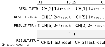
Example of RAM placement (even RESULT.MAXCNT), channels 1, 2 and 5 enabled provides an example of results placement in Data RAM, with an even RESULT.MAXCNT. In this example, channels 1, 2 and 5 are enabled, all others are disabled.
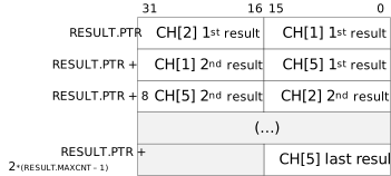
Example of RAM placement (odd RESULT.MAXCNT), channels 1, 2 and 5 enabled provides an example of results placement in Data RAM, with an odd RESULT.MAXCNT. In this example, channels 1, 2 and 5 are enabled, all others are disabled. The last 32-bit word is populated only with one 16-bit result.
EasyDMA
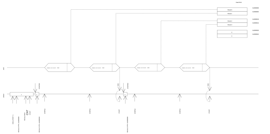
After configuring RESULT.PTR and RESULT.MAXCNT, the ADC resources are started by triggering the START task. The ADC is using EasyDMA to store results in a Result buffer in RAM.
The Result buffer is located at the address specified in the RESULT.PTR register. The RESULT.PTR register is double-buffered and it can be updated and prepared for the next START task immediately after the STARTED event is generated. The size of the Result buffer is specified in the RESULT.MAXCNT register and the ADC will generate an END event when it has filled up the Result buffer, see ADC. Results are stored in little-endian byte order in Data RAM. Every sample will be sign extended to 16 bit before stored in the Result buffer.
The ADC is stopped by triggering the STOP task. The STOP task will terminate an ongoing sampling. The ADC will generate a STOPPED event when it has stopped. If the ADC is already stopped when the STOP task is triggered, the STOPPED event will still be generated.
If the RESULT.PTR is not pointing to the Data RAM region, an EasyDMA transfer may result in a HardFault or RAM corruption. See Memory for more information about the different memory regions.
The EasyDMA will have finished accessing the RAM when the END or STOPPED event has been generated.
The RESULT.AMOUNT register can be read following an END event or a STOPPED event to see how many results have been transferred to the Result buffer in RAM since the START task was triggered.
In scan mode, SAMPLE tasks can be triggered once the START task is triggered. The END event is generated when the number of samples transferred to memory reaches the value specified by RESULT.MAXCNT. After an END event, the START task needs to be triggered again before new samples can be taken. Also make sure that the size of the Result buffer is large enough to have space for minimum one result from each of the enabled channels, by specifying RESULT.MAXCNT >= number of channels enabled. For more information about the scan mode, see Scan mode.
Resistor ladder
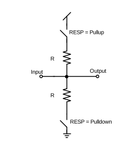
The ADC has an internal resistor string for positive and negative input.
See Resistor ladder for positive input (negative input is equivalent, using RESN instead of RESP). The resistors are controlled in the CH[n].CONFIG.RESP and CH[n].CONFIG.RESN registers.
Reference
The ADC can use two different references, controlled in the REFSEL field of the CH[n].CONFIG register.
These are:
- Internal reference
- VDD as reference
The internal reference results in an input range of ±0.6 V on the ADC core. VDD as reference results in an input range of ±VDD/4 on the ADC core. The gain block can be used to change the effective input range of the ADC.
Input range = (+- 0.6 V or +-VDD/4)/GainFor example, choosing VDD as reference, single ended input (grounded negative input), and a gain of 1/4 the input range will be:
Input range = (VDD/4)/(1/4) = VDDWith internal reference, single ended input (grounded negative input), and a gain of 1/6 the input range will be:
Input range = (0.6 V)/(1/6) = 3.6 VThe AIN0-AIN7 inputs cannot exceed VDD, or be lower than VSS.
Acquisition time
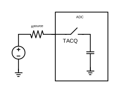
To sample the input voltage, the ADC connects a capacitor to the input.
For illustration, see Simplified ADC sample network. The acquisition time indicates how long the capacitor is connected, see TACQ field in CH[n].CONFIG register. The required acquisition time depends on the source (Rsource) resistance. For high source resistance the acquisition time should be increased, see Acquisition time.
| TACQ [µs] | Maximum source resistance [kOhm] |
|---|---|
| 3 | 10 |
| 5 | 40 |
| 10 | 100 |
| 15 | 200 |
| 20 | 400 |
| 40 | 800 |
Limits event monitoring
A channel can be event monitored by configuring limit register CH[n].LIMIT.
If the conversion result is higher than the defined high limit, or lower than the defined low limit, the appropriate event will get fired.
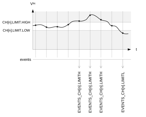
Note that when setting the limits, CH[n].LIMIT.HIGH shall always be higher than or equal to CH[n].LIMIT.LOW . In other words, an event can be fired only when the input signal has been sampled outside of the defined limits. It is not possible to fire an event when the input signal is inside a defined range by swapping high and low limits.
The comparison to limits always takes place, there is no need to enable it. If comparison is not required on a channel, the software shall simply ignore the related events. In that situation, the value of the limits registers is irrelevant, so it does not matter if CH[n].LIMIT.LOW is lower than CH[n].LIMIT.HIGH or not.
Registers
| Base address | Peripheral | Instance | Description | Configuration | |
|---|---|---|---|---|---|
| 0x40007000 | SAADC | SAADC | Analog-to-digital converter | ||
| Register | Offset | Description | |
|---|---|---|---|
| TASKS_START | 0x000 | Start the ADC and prepare the result buffer in RAM | |
| TASKS_SAMPLE | 0x004 | Take one ADC sample, if scan is enabled all channels are sampled | |
| TASKS_STOP | 0x008 | Stop the ADC and terminate any on-going conversion | |
| TASKS_CALIBRATEOFFSET | 0x00C | Starts offset auto-calibration | |
| EVENTS_STARTED | 0x100 | The ADC has started | |
| EVENTS_END | 0x104 | The ADC has filled up the Result buffer | |
| EVENTS_DONE | 0x108 | A conversion task has been completed. Depending on the mode, multiple conversions might be needed for a result to be transferred to RAM. | |
| EVENTS_RESULTDONE | 0x10C | A result is ready to get transferred to RAM. | |
| EVENTS_CALIBRATEDONE | 0x110 | Calibration is complete | |
| EVENTS_STOPPED | 0x114 | The ADC has stopped | |
| EVENTS_CH[0].LIMITH | 0x118 | Last results is equal or above CH[0].LIMIT.HIGH | |
| EVENTS_CH[0].LIMITL | 0x11C | Last results is equal or below CH[0].LIMIT.LOW | |
| EVENTS_CH[1].LIMITH | 0x120 | Last results is equal or above CH[1].LIMIT.HIGH | |
| EVENTS_CH[1].LIMITL | 0x124 | Last results is equal or below CH[1].LIMIT.LOW | |
| EVENTS_CH[2].LIMITH | 0x128 | Last results is equal or above CH[2].LIMIT.HIGH | |
| EVENTS_CH[2].LIMITL | 0x12C | Last results is equal or below CH[2].LIMIT.LOW | |
| EVENTS_CH[3].LIMITH | 0x130 | Last results is equal or above CH[3].LIMIT.HIGH | |
| EVENTS_CH[3].LIMITL | 0x134 | Last results is equal or below CH[3].LIMIT.LOW | |
| EVENTS_CH[4].LIMITH | 0x138 | Last results is equal or above CH[4].LIMIT.HIGH | |
| EVENTS_CH[4].LIMITL | 0x13C | Last results is equal or below CH[4].LIMIT.LOW | |
| EVENTS_CH[5].LIMITH | 0x140 | Last results is equal or above CH[5].LIMIT.HIGH | |
| EVENTS_CH[5].LIMITL | 0x144 | Last results is equal or below CH[5].LIMIT.LOW | |
| EVENTS_CH[6].LIMITH | 0x148 | Last results is equal or above CH[6].LIMIT.HIGH | |
| EVENTS_CH[6].LIMITL | 0x14C | Last results is equal or below CH[6].LIMIT.LOW | |
| EVENTS_CH[7].LIMITH | 0x150 | Last results is equal or above CH[7].LIMIT.HIGH | |
| EVENTS_CH[7].LIMITL | 0x154 | Last results is equal or below CH[7].LIMIT.LOW | |
| INTEN | 0x300 | Enable or disable interrupt | |
| INTENSET | 0x304 | Enable interrupt | |
| INTENCLR | 0x308 | Disable interrupt | |
| STATUS | 0x400 | Status | |
| ENABLE | 0x500 | Enable or disable ADC | |
| CH[0].PSELP | 0x510 | Input positive pin selection for CH[0] | |
| CH[0].PSELN | 0x514 | Input negative pin selection for CH[0] | |
| CH[0].CONFIG | 0x518 | Input configuration for CH[0] | |
| CH[0].LIMIT | 0x51C | High/low limits for event monitoring a channel | |
| CH[1].PSELP | 0x520 | Input positive pin selection for CH[1] | |
| CH[1].PSELN | 0x524 | Input negative pin selection for CH[1] | |
| CH[1].CONFIG | 0x528 | Input configuration for CH[1] | |
| CH[1].LIMIT | 0x52C | High/low limits for event monitoring a channel | |
| CH[2].PSELP | 0x530 | Input positive pin selection for CH[2] | |
| CH[2].PSELN | 0x534 | Input negative pin selection for CH[2] | |
| CH[2].CONFIG | 0x538 | Input configuration for CH[2] | |
| CH[2].LIMIT | 0x53C | High/low limits for event monitoring a channel | |
| CH[3].PSELP | 0x540 | Input positive pin selection for CH[3] | |
| CH[3].PSELN | 0x544 | Input negative pin selection for CH[3] | |
| CH[3].CONFIG | 0x548 | Input configuration for CH[3] | |
| CH[3].LIMIT | 0x54C | High/low limits for event monitoring a channel | |
| CH[4].PSELP | 0x550 | Input positive pin selection for CH[4] | |
| CH[4].PSELN | 0x554 | Input negative pin selection for CH[4] | |
| CH[4].CONFIG | 0x558 | Input configuration for CH[4] | |
| CH[4].LIMIT | 0x55C | High/low limits for event monitoring a channel | |
| CH[5].PSELP | 0x560 | Input positive pin selection for CH[5] | |
| CH[5].PSELN | 0x564 | Input negative pin selection for CH[5] | |
| CH[5].CONFIG | 0x568 | Input configuration for CH[5] | |
| CH[5].LIMIT | 0x56C | High/low limits for event monitoring a channel | |
| CH[6].PSELP | 0x570 | Input positive pin selection for CH[6] | |
| CH[6].PSELN | 0x574 | Input negative pin selection for CH[6] | |
| CH[6].CONFIG | 0x578 | Input configuration for CH[6] | |
| CH[6].LIMIT | 0x57C | High/low limits for event monitoring a channel | |
| CH[7].PSELP | 0x580 | Input positive pin selection for CH[7] | |
| CH[7].PSELN | 0x584 | Input negative pin selection for CH[7] | |
| CH[7].CONFIG | 0x588 | Input configuration for CH[7] | |
| CH[7].LIMIT | 0x58C | High/low limits for event monitoring a channel | |
| RESOLUTION | 0x5F0 | Resolution configuration | |
| OVERSAMPLE | 0x5F4 | Oversampling configuration. OVERSAMPLE should not be combined with SCAN. The RESOLUTION is applied before averaging, thus for high OVERSAMPLE a higher RESOLUTION should be used. | |
| SAMPLERATE | 0x5F8 | Controls normal or continuous sample rate | |
| RESULT.PTR | 0x62C | Data pointer | |
| RESULT.MAXCNT | 0x630 | Maximum number of buffer words to transfer | |
| RESULT.AMOUNT | 0x634 | Number of buffer words transferred since last START | |
TASKS_START
Address offset: 0x000
Start the ADC and prepare the result buffer in RAM
| Bit number | 31 | 30 | 29 | 28 | 27 | 26 | 25 | 24 | 23 | 22 | 21 | 20 | 19 | 18 | 17 | 16 | 15 | 14 | 13 | 12 | 11 | 10 | 9 | 8 | 7 | 6 | 5 | 4 | 3 | 2 | 1 | 0 | |||
|---|---|---|---|---|---|---|---|---|---|---|---|---|---|---|---|---|---|---|---|---|---|---|---|---|---|---|---|---|---|---|---|---|---|---|---|
| ID | A | ||||||||||||||||||||||||||||||||||
| Reset 0x00000000 | 0 | 0 | 0 | 0 | 0 | 0 | 0 | 0 | 0 | 0 | 0 | 0 | 0 | 0 | 0 | 0 | 0 | 0 | 0 | 0 | 0 | 0 | 0 | 0 | 0 | 0 | 0 | 0 | 0 | 0 | 0 | 0 | |||
| ID | Access | Field | Value ID | Value | Description | ||||||||||||||||||||||||||||||
| A | W | TASKS_START | Start the ADC and prepare the result buffer in RAM | ||||||||||||||||||||||||||||||||
Trigger | 1 | Trigger task | |||||||||||||||||||||||||||||||||
TASKS_SAMPLE
Address offset: 0x004
Take one ADC sample, if scan is enabled all channels are sampled
| Bit number | 31 | 30 | 29 | 28 | 27 | 26 | 25 | 24 | 23 | 22 | 21 | 20 | 19 | 18 | 17 | 16 | 15 | 14 | 13 | 12 | 11 | 10 | 9 | 8 | 7 | 6 | 5 | 4 | 3 | 2 | 1 | 0 | |||
|---|---|---|---|---|---|---|---|---|---|---|---|---|---|---|---|---|---|---|---|---|---|---|---|---|---|---|---|---|---|---|---|---|---|---|---|
| ID | A | ||||||||||||||||||||||||||||||||||
| Reset 0x00000000 | 0 | 0 | 0 | 0 | 0 | 0 | 0 | 0 | 0 | 0 | 0 | 0 | 0 | 0 | 0 | 0 | 0 | 0 | 0 | 0 | 0 | 0 | 0 | 0 | 0 | 0 | 0 | 0 | 0 | 0 | 0 | 0 | |||
| ID | Access | Field | Value ID | Value | Description | ||||||||||||||||||||||||||||||
| A | W | TASKS_SAMPLE | Take one ADC sample, if scan is enabled all channels are sampled | ||||||||||||||||||||||||||||||||
Trigger | 1 | Trigger task | |||||||||||||||||||||||||||||||||
TASKS_STOP
Address offset: 0x008
Stop the ADC and terminate any on-going conversion
| Bit number | 31 | 30 | 29 | 28 | 27 | 26 | 25 | 24 | 23 | 22 | 21 | 20 | 19 | 18 | 17 | 16 | 15 | 14 | 13 | 12 | 11 | 10 | 9 | 8 | 7 | 6 | 5 | 4 | 3 | 2 | 1 | 0 | |||
|---|---|---|---|---|---|---|---|---|---|---|---|---|---|---|---|---|---|---|---|---|---|---|---|---|---|---|---|---|---|---|---|---|---|---|---|
| ID | A | ||||||||||||||||||||||||||||||||||
| Reset 0x00000000 | 0 | 0 | 0 | 0 | 0 | 0 | 0 | 0 | 0 | 0 | 0 | 0 | 0 | 0 | 0 | 0 | 0 | 0 | 0 | 0 | 0 | 0 | 0 | 0 | 0 | 0 | 0 | 0 | 0 | 0 | 0 | 0 | |||
| ID | Access | Field | Value ID | Value | Description | ||||||||||||||||||||||||||||||
| A | W | TASKS_STOP | Stop the ADC and terminate any on-going conversion | ||||||||||||||||||||||||||||||||
Trigger | 1 | Trigger task | |||||||||||||||||||||||||||||||||
TASKS_CALIBRATEOFFSET
Address offset: 0x00C
Starts offset auto-calibration
| Bit number | 31 | 30 | 29 | 28 | 27 | 26 | 25 | 24 | 23 | 22 | 21 | 20 | 19 | 18 | 17 | 16 | 15 | 14 | 13 | 12 | 11 | 10 | 9 | 8 | 7 | 6 | 5 | 4 | 3 | 2 | 1 | 0 | |||
|---|---|---|---|---|---|---|---|---|---|---|---|---|---|---|---|---|---|---|---|---|---|---|---|---|---|---|---|---|---|---|---|---|---|---|---|
| ID | A | ||||||||||||||||||||||||||||||||||
| Reset 0x00000000 | 0 | 0 | 0 | 0 | 0 | 0 | 0 | 0 | 0 | 0 | 0 | 0 | 0 | 0 | 0 | 0 | 0 | 0 | 0 | 0 | 0 | 0 | 0 | 0 | 0 | 0 | 0 | 0 | 0 | 0 | 0 | 0 | |||
| ID | Access | Field | Value ID | Value | Description | ||||||||||||||||||||||||||||||
| A | W | TASKS_CALIBRATEOFFSET | Starts offset auto-calibration | ||||||||||||||||||||||||||||||||
Trigger | 1 | Trigger task | |||||||||||||||||||||||||||||||||
EVENTS_STARTED
Address offset: 0x100
The ADC has started
| Bit number | 31 | 30 | 29 | 28 | 27 | 26 | 25 | 24 | 23 | 22 | 21 | 20 | 19 | 18 | 17 | 16 | 15 | 14 | 13 | 12 | 11 | 10 | 9 | 8 | 7 | 6 | 5 | 4 | 3 | 2 | 1 | 0 | |||
|---|---|---|---|---|---|---|---|---|---|---|---|---|---|---|---|---|---|---|---|---|---|---|---|---|---|---|---|---|---|---|---|---|---|---|---|
| ID | A | ||||||||||||||||||||||||||||||||||
| Reset 0x00000000 | 0 | 0 | 0 | 0 | 0 | 0 | 0 | 0 | 0 | 0 | 0 | 0 | 0 | 0 | 0 | 0 | 0 | 0 | 0 | 0 | 0 | 0 | 0 | 0 | 0 | 0 | 0 | 0 | 0 | 0 | 0 | 0 | |||
| ID | Access | Field | Value ID | Value | Description | ||||||||||||||||||||||||||||||
| A | RW | EVENTS_STARTED | The ADC has started | ||||||||||||||||||||||||||||||||
NotGenerated | 0 | Event not generated | |||||||||||||||||||||||||||||||||
Generated | 1 | Event generated | |||||||||||||||||||||||||||||||||
EVENTS_END
Address offset: 0x104
The ADC has filled up the Result buffer
| Bit number | 31 | 30 | 29 | 28 | 27 | 26 | 25 | 24 | 23 | 22 | 21 | 20 | 19 | 18 | 17 | 16 | 15 | 14 | 13 | 12 | 11 | 10 | 9 | 8 | 7 | 6 | 5 | 4 | 3 | 2 | 1 | 0 | |||
|---|---|---|---|---|---|---|---|---|---|---|---|---|---|---|---|---|---|---|---|---|---|---|---|---|---|---|---|---|---|---|---|---|---|---|---|
| ID | A | ||||||||||||||||||||||||||||||||||
| Reset 0x00000000 | 0 | 0 | 0 | 0 | 0 | 0 | 0 | 0 | 0 | 0 | 0 | 0 | 0 | 0 | 0 | 0 | 0 | 0 | 0 | 0 | 0 | 0 | 0 | 0 | 0 | 0 | 0 | 0 | 0 | 0 | 0 | 0 | |||
| ID | Access | Field | Value ID | Value | Description | ||||||||||||||||||||||||||||||
| A | RW | EVENTS_END | The ADC has filled up the Result buffer | ||||||||||||||||||||||||||||||||
NotGenerated | 0 | Event not generated | |||||||||||||||||||||||||||||||||
Generated | 1 | Event generated | |||||||||||||||||||||||||||||||||
EVENTS_DONE
Address offset: 0x108
A conversion task has been completed. Depending on the mode, multiple conversions might be needed for a result to be transferred to RAM.
| Bit number | 31 | 30 | 29 | 28 | 27 | 26 | 25 | 24 | 23 | 22 | 21 | 20 | 19 | 18 | 17 | 16 | 15 | 14 | 13 | 12 | 11 | 10 | 9 | 8 | 7 | 6 | 5 | 4 | 3 | 2 | 1 | 0 | |||
|---|---|---|---|---|---|---|---|---|---|---|---|---|---|---|---|---|---|---|---|---|---|---|---|---|---|---|---|---|---|---|---|---|---|---|---|
| ID | A | ||||||||||||||||||||||||||||||||||
| Reset 0x00000000 | 0 | 0 | 0 | 0 | 0 | 0 | 0 | 0 | 0 | 0 | 0 | 0 | 0 | 0 | 0 | 0 | 0 | 0 | 0 | 0 | 0 | 0 | 0 | 0 | 0 | 0 | 0 | 0 | 0 | 0 | 0 | 0 | |||
| ID | Access | Field | Value ID | Value | Description | ||||||||||||||||||||||||||||||
| A | RW | EVENTS_DONE | A conversion task has been completed. Depending on the mode, multiple conversions might be needed for a result to be transferred to RAM. | ||||||||||||||||||||||||||||||||
NotGenerated | 0 | Event not generated | |||||||||||||||||||||||||||||||||
Generated | 1 | Event generated | |||||||||||||||||||||||||||||||||
EVENTS_RESULTDONE
Address offset: 0x10C
A result is ready to get transferred to RAM.
| Bit number | 31 | 30 | 29 | 28 | 27 | 26 | 25 | 24 | 23 | 22 | 21 | 20 | 19 | 18 | 17 | 16 | 15 | 14 | 13 | 12 | 11 | 10 | 9 | 8 | 7 | 6 | 5 | 4 | 3 | 2 | 1 | 0 | |||
|---|---|---|---|---|---|---|---|---|---|---|---|---|---|---|---|---|---|---|---|---|---|---|---|---|---|---|---|---|---|---|---|---|---|---|---|
| ID | A | ||||||||||||||||||||||||||||||||||
| Reset 0x00000000 | 0 | 0 | 0 | 0 | 0 | 0 | 0 | 0 | 0 | 0 | 0 | 0 | 0 | 0 | 0 | 0 | 0 | 0 | 0 | 0 | 0 | 0 | 0 | 0 | 0 | 0 | 0 | 0 | 0 | 0 | 0 | 0 | |||
| ID | Access | Field | Value ID | Value | Description | ||||||||||||||||||||||||||||||
| A | RW | EVENTS_RESULTDONE | A result is ready to get transferred to RAM. | ||||||||||||||||||||||||||||||||
NotGenerated | 0 | Event not generated | |||||||||||||||||||||||||||||||||
Generated | 1 | Event generated | |||||||||||||||||||||||||||||||||
EVENTS_CALIBRATEDONE
Address offset: 0x110
Calibration is complete
| Bit number | 31 | 30 | 29 | 28 | 27 | 26 | 25 | 24 | 23 | 22 | 21 | 20 | 19 | 18 | 17 | 16 | 15 | 14 | 13 | 12 | 11 | 10 | 9 | 8 | 7 | 6 | 5 | 4 | 3 | 2 | 1 | 0 | |||
|---|---|---|---|---|---|---|---|---|---|---|---|---|---|---|---|---|---|---|---|---|---|---|---|---|---|---|---|---|---|---|---|---|---|---|---|
| ID | A | ||||||||||||||||||||||||||||||||||
| Reset 0x00000000 | 0 | 0 | 0 | 0 | 0 | 0 | 0 | 0 | 0 | 0 | 0 | 0 | 0 | 0 | 0 | 0 | 0 | 0 | 0 | 0 | 0 | 0 | 0 | 0 | 0 | 0 | 0 | 0 | 0 | 0 | 0 | 0 | |||
| ID | Access | Field | Value ID | Value | Description | ||||||||||||||||||||||||||||||
| A | RW | EVENTS_CALIBRATEDONE | Calibration is complete | ||||||||||||||||||||||||||||||||
NotGenerated | 0 | Event not generated | |||||||||||||||||||||||||||||||||
Generated | 1 | Event generated | |||||||||||||||||||||||||||||||||
EVENTS_STOPPED
Address offset: 0x114
The ADC has stopped
| Bit number | 31 | 30 | 29 | 28 | 27 | 26 | 25 | 24 | 23 | 22 | 21 | 20 | 19 | 18 | 17 | 16 | 15 | 14 | 13 | 12 | 11 | 10 | 9 | 8 | 7 | 6 | 5 | 4 | 3 | 2 | 1 | 0 | |||
|---|---|---|---|---|---|---|---|---|---|---|---|---|---|---|---|---|---|---|---|---|---|---|---|---|---|---|---|---|---|---|---|---|---|---|---|
| ID | A | ||||||||||||||||||||||||||||||||||
| Reset 0x00000000 | 0 | 0 | 0 | 0 | 0 | 0 | 0 | 0 | 0 | 0 | 0 | 0 | 0 | 0 | 0 | 0 | 0 | 0 | 0 | 0 | 0 | 0 | 0 | 0 | 0 | 0 | 0 | 0 | 0 | 0 | 0 | 0 | |||
| ID | Access | Field | Value ID | Value | Description | ||||||||||||||||||||||||||||||
| A | RW | EVENTS_STOPPED | The ADC has stopped | ||||||||||||||||||||||||||||||||
NotGenerated | 0 | Event not generated | |||||||||||||||||||||||||||||||||
Generated | 1 | Event generated | |||||||||||||||||||||||||||||||||
EVENTS_CH[n].LIMITH (n=0..7)
Address offset: 0x118 + (n × 0x8)
Last results is equal or above CH[n].LIMIT.HIGH
| Bit number | 31 | 30 | 29 | 28 | 27 | 26 | 25 | 24 | 23 | 22 | 21 | 20 | 19 | 18 | 17 | 16 | 15 | 14 | 13 | 12 | 11 | 10 | 9 | 8 | 7 | 6 | 5 | 4 | 3 | 2 | 1 | 0 | |||
|---|---|---|---|---|---|---|---|---|---|---|---|---|---|---|---|---|---|---|---|---|---|---|---|---|---|---|---|---|---|---|---|---|---|---|---|
| ID | A | ||||||||||||||||||||||||||||||||||
| Reset 0x00000000 | 0 | 0 | 0 | 0 | 0 | 0 | 0 | 0 | 0 | 0 | 0 | 0 | 0 | 0 | 0 | 0 | 0 | 0 | 0 | 0 | 0 | 0 | 0 | 0 | 0 | 0 | 0 | 0 | 0 | 0 | 0 | 0 | |||
| ID | Access | Field | Value ID | Value | Description | ||||||||||||||||||||||||||||||
| A | RW | LIMITH | Last results is equal or above CH[n].LIMIT.HIGH | ||||||||||||||||||||||||||||||||
NotGenerated | 0 | Event not generated | |||||||||||||||||||||||||||||||||
Generated | 1 | Event generated | |||||||||||||||||||||||||||||||||
EVENTS_CH[n].LIMITL (n=0..7)
Address offset: 0x11C + (n × 0x8)
Last results is equal or below CH[n].LIMIT.LOW
| Bit number | 31 | 30 | 29 | 28 | 27 | 26 | 25 | 24 | 23 | 22 | 21 | 20 | 19 | 18 | 17 | 16 | 15 | 14 | 13 | 12 | 11 | 10 | 9 | 8 | 7 | 6 | 5 | 4 | 3 | 2 | 1 | 0 | |||
|---|---|---|---|---|---|---|---|---|---|---|---|---|---|---|---|---|---|---|---|---|---|---|---|---|---|---|---|---|---|---|---|---|---|---|---|
| ID | A | ||||||||||||||||||||||||||||||||||
| Reset 0x00000000 | 0 | 0 | 0 | 0 | 0 | 0 | 0 | 0 | 0 | 0 | 0 | 0 | 0 | 0 | 0 | 0 | 0 | 0 | 0 | 0 | 0 | 0 | 0 | 0 | 0 | 0 | 0 | 0 | 0 | 0 | 0 | 0 | |||
| ID | Access | Field | Value ID | Value | Description | ||||||||||||||||||||||||||||||
| A | RW | LIMITL | Last results is equal or below CH[n].LIMIT.LOW | ||||||||||||||||||||||||||||||||
NotGenerated | 0 | Event not generated | |||||||||||||||||||||||||||||||||
Generated | 1 | Event generated | |||||||||||||||||||||||||||||||||
INTEN
Address offset: 0x300
Enable or disable interrupt
| Bit number | 31 | 30 | 29 | 28 | 27 | 26 | 25 | 24 | 23 | 22 | 21 | 20 | 19 | 18 | 17 | 16 | 15 | 14 | 13 | 12 | 11 | 10 | 9 | 8 | 7 | 6 | 5 | 4 | 3 | 2 | 1 | 0 | |||
|---|---|---|---|---|---|---|---|---|---|---|---|---|---|---|---|---|---|---|---|---|---|---|---|---|---|---|---|---|---|---|---|---|---|---|---|
| ID | V | U | T | S | R | Q | P | O | N | M | L | K | J | I | H | G | F | E | D | C | B | A | |||||||||||||
| Reset 0x00000000 | 0 | 0 | 0 | 0 | 0 | 0 | 0 | 0 | 0 | 0 | 0 | 0 | 0 | 0 | 0 | 0 | 0 | 0 | 0 | 0 | 0 | 0 | 0 | 0 | 0 | 0 | 0 | 0 | 0 | 0 | 0 | 0 | |||
| ID | Access | Field | Value ID | Value | Description | ||||||||||||||||||||||||||||||
| A | RW | STARTED | Enable or disable interrupt for event STARTED | ||||||||||||||||||||||||||||||||
Disabled | 0 | Disable | |||||||||||||||||||||||||||||||||
Enabled | 1 | Enable | |||||||||||||||||||||||||||||||||
| B | RW | END | Enable or disable interrupt for event END | ||||||||||||||||||||||||||||||||
Disabled | 0 | Disable | |||||||||||||||||||||||||||||||||
Enabled | 1 | Enable | |||||||||||||||||||||||||||||||||
| C | RW | DONE | Enable or disable interrupt for event DONE | ||||||||||||||||||||||||||||||||
Disabled | 0 | Disable | |||||||||||||||||||||||||||||||||
Enabled | 1 | Enable | |||||||||||||||||||||||||||||||||
| D | RW | RESULTDONE | Enable or disable interrupt for event RESULTDONE | ||||||||||||||||||||||||||||||||
Disabled | 0 | Disable | |||||||||||||||||||||||||||||||||
Enabled | 1 | Enable | |||||||||||||||||||||||||||||||||
| E | RW | CALIBRATEDONE | Enable or disable interrupt for event CALIBRATEDONE | ||||||||||||||||||||||||||||||||
Disabled | 0 | Disable | |||||||||||||||||||||||||||||||||
Enabled | 1 | Enable | |||||||||||||||||||||||||||||||||
| F | RW | STOPPED | Enable or disable interrupt for event STOPPED | ||||||||||||||||||||||||||||||||
Disabled | 0 | Disable | |||||||||||||||||||||||||||||||||
Enabled | 1 | Enable | |||||||||||||||||||||||||||||||||
| G | RW | CH0LIMITH | Enable or disable interrupt for event CH0LIMITH | ||||||||||||||||||||||||||||||||
Disabled | 0 | Disable | |||||||||||||||||||||||||||||||||
Enabled | 1 | Enable | |||||||||||||||||||||||||||||||||
| H | RW | CH0LIMITL | Enable or disable interrupt for event CH0LIMITL | ||||||||||||||||||||||||||||||||
Disabled | 0 | Disable | |||||||||||||||||||||||||||||||||
Enabled | 1 | Enable | |||||||||||||||||||||||||||||||||
| I | RW | CH1LIMITH | Enable or disable interrupt for event CH1LIMITH | ||||||||||||||||||||||||||||||||
Disabled | 0 | Disable | |||||||||||||||||||||||||||||||||
Enabled | 1 | Enable | |||||||||||||||||||||||||||||||||
| J | RW | CH1LIMITL | Enable or disable interrupt for event CH1LIMITL | ||||||||||||||||||||||||||||||||
Disabled | 0 | Disable | |||||||||||||||||||||||||||||||||
Enabled | 1 | Enable | |||||||||||||||||||||||||||||||||
| K | RW | CH2LIMITH | Enable or disable interrupt for event CH2LIMITH | ||||||||||||||||||||||||||||||||
Disabled | 0 | Disable | |||||||||||||||||||||||||||||||||
Enabled | 1 | Enable | |||||||||||||||||||||||||||||||||
| L | RW | CH2LIMITL | Enable or disable interrupt for event CH2LIMITL | ||||||||||||||||||||||||||||||||
Disabled | 0 | Disable | |||||||||||||||||||||||||||||||||
Enabled | 1 | Enable | |||||||||||||||||||||||||||||||||
| M | RW | CH3LIMITH | Enable or disable interrupt for event CH3LIMITH | ||||||||||||||||||||||||||||||||
Disabled | 0 | Disable | |||||||||||||||||||||||||||||||||
Enabled | 1 | Enable | |||||||||||||||||||||||||||||||||
| N | RW | CH3LIMITL | Enable or disable interrupt for event CH3LIMITL | ||||||||||||||||||||||||||||||||
Disabled | 0 | Disable | |||||||||||||||||||||||||||||||||
Enabled | 1 | Enable | |||||||||||||||||||||||||||||||||
| O | RW | CH4LIMITH | Enable or disable interrupt for event CH4LIMITH | ||||||||||||||||||||||||||||||||
Disabled | 0 | Disable | |||||||||||||||||||||||||||||||||
Enabled | 1 | Enable | |||||||||||||||||||||||||||||||||
| P | RW | CH4LIMITL | Enable or disable interrupt for event CH4LIMITL | ||||||||||||||||||||||||||||||||
Disabled | 0 | Disable | |||||||||||||||||||||||||||||||||
Enabled | 1 | Enable | |||||||||||||||||||||||||||||||||
| Q | RW | CH5LIMITH | Enable or disable interrupt for event CH5LIMITH | ||||||||||||||||||||||||||||||||
Disabled | 0 | Disable | |||||||||||||||||||||||||||||||||
Enabled | 1 | Enable | |||||||||||||||||||||||||||||||||
| R | RW | CH5LIMITL | Enable or disable interrupt for event CH5LIMITL | ||||||||||||||||||||||||||||||||
Disabled | 0 | Disable | |||||||||||||||||||||||||||||||||
Enabled | 1 | Enable | |||||||||||||||||||||||||||||||||
| S | RW | CH6LIMITH | Enable or disable interrupt for event CH6LIMITH | ||||||||||||||||||||||||||||||||
Disabled | 0 | Disable | |||||||||||||||||||||||||||||||||
Enabled | 1 | Enable | |||||||||||||||||||||||||||||||||
| T | RW | CH6LIMITL | Enable or disable interrupt for event CH6LIMITL | ||||||||||||||||||||||||||||||||
Disabled | 0 | Disable | |||||||||||||||||||||||||||||||||
Enabled | 1 | Enable | |||||||||||||||||||||||||||||||||
| U | RW | CH7LIMITH | Enable or disable interrupt for event CH7LIMITH | ||||||||||||||||||||||||||||||||
Disabled | 0 | Disable | |||||||||||||||||||||||||||||||||
Enabled | 1 | Enable | |||||||||||||||||||||||||||||||||
| V | RW | CH7LIMITL | Enable or disable interrupt for event CH7LIMITL | ||||||||||||||||||||||||||||||||
Disabled | 0 | Disable | |||||||||||||||||||||||||||||||||
Enabled | 1 | Enable | |||||||||||||||||||||||||||||||||
INTENSET
Address offset: 0x304
Enable interrupt
| Bit number | 31 | 30 | 29 | 28 | 27 | 26 | 25 | 24 | 23 | 22 | 21 | 20 | 19 | 18 | 17 | 16 | 15 | 14 | 13 | 12 | 11 | 10 | 9 | 8 | 7 | 6 | 5 | 4 | 3 | 2 | 1 | 0 | |||
|---|---|---|---|---|---|---|---|---|---|---|---|---|---|---|---|---|---|---|---|---|---|---|---|---|---|---|---|---|---|---|---|---|---|---|---|
| ID | V | U | T | S | R | Q | P | O | N | M | L | K | J | I | H | G | F | E | D | C | B | A | |||||||||||||
| Reset 0x00000000 | 0 | 0 | 0 | 0 | 0 | 0 | 0 | 0 | 0 | 0 | 0 | 0 | 0 | 0 | 0 | 0 | 0 | 0 | 0 | 0 | 0 | 0 | 0 | 0 | 0 | 0 | 0 | 0 | 0 | 0 | 0 | 0 | |||
| ID | Access | Field | Value ID | Value | Description | ||||||||||||||||||||||||||||||
| A | RW | STARTED | Write '1' to enable interrupt for event STARTED | ||||||||||||||||||||||||||||||||
Set | 1 | Enable | |||||||||||||||||||||||||||||||||
Disabled | 0 | Read: Disabled | |||||||||||||||||||||||||||||||||
Enabled | 1 | Read: Enabled | |||||||||||||||||||||||||||||||||
| B | RW | END | Write '1' to enable interrupt for event END | ||||||||||||||||||||||||||||||||
Set | 1 | Enable | |||||||||||||||||||||||||||||||||
Disabled | 0 | Read: Disabled | |||||||||||||||||||||||||||||||||
Enabled | 1 | Read: Enabled | |||||||||||||||||||||||||||||||||
| C | RW | DONE | Write '1' to enable interrupt for event DONE | ||||||||||||||||||||||||||||||||
Set | 1 | Enable | |||||||||||||||||||||||||||||||||
Disabled | 0 | Read: Disabled | |||||||||||||||||||||||||||||||||
Enabled | 1 | Read: Enabled | |||||||||||||||||||||||||||||||||
| D | RW | RESULTDONE | Write '1' to enable interrupt for event RESULTDONE | ||||||||||||||||||||||||||||||||
Set | 1 | Enable | |||||||||||||||||||||||||||||||||
Disabled | 0 | Read: Disabled | |||||||||||||||||||||||||||||||||
Enabled | 1 | Read: Enabled | |||||||||||||||||||||||||||||||||
| E | RW | CALIBRATEDONE | Write '1' to enable interrupt for event CALIBRATEDONE | ||||||||||||||||||||||||||||||||
Set | 1 | Enable | |||||||||||||||||||||||||||||||||
Disabled | 0 | Read: Disabled | |||||||||||||||||||||||||||||||||
Enabled | 1 | Read: Enabled | |||||||||||||||||||||||||||||||||
| F | RW | STOPPED | Write '1' to enable interrupt for event STOPPED | ||||||||||||||||||||||||||||||||
Set | 1 | Enable | |||||||||||||||||||||||||||||||||
Disabled | 0 | Read: Disabled | |||||||||||||||||||||||||||||||||
Enabled | 1 | Read: Enabled | |||||||||||||||||||||||||||||||||
| G | RW | CH0LIMITH | Write '1' to enable interrupt for event CH0LIMITH | ||||||||||||||||||||||||||||||||
Set | 1 | Enable | |||||||||||||||||||||||||||||||||
Disabled | 0 | Read: Disabled | |||||||||||||||||||||||||||||||||
Enabled | 1 | Read: Enabled | |||||||||||||||||||||||||||||||||
| H | RW | CH0LIMITL | Write '1' to enable interrupt for event CH0LIMITL | ||||||||||||||||||||||||||||||||
Set | 1 | Enable | |||||||||||||||||||||||||||||||||
Disabled | 0 | Read: Disabled | |||||||||||||||||||||||||||||||||
Enabled | 1 | Read: Enabled | |||||||||||||||||||||||||||||||||
| I | RW | CH1LIMITH | Write '1' to enable interrupt for event CH1LIMITH | ||||||||||||||||||||||||||||||||
Set | 1 | Enable | |||||||||||||||||||||||||||||||||
Disabled | 0 | Read: Disabled | |||||||||||||||||||||||||||||||||
Enabled | 1 | Read: Enabled | |||||||||||||||||||||||||||||||||
| J | RW | CH1LIMITL | Write '1' to enable interrupt for event CH1LIMITL | ||||||||||||||||||||||||||||||||
Set | 1 | Enable | |||||||||||||||||||||||||||||||||
Disabled | 0 | Read: Disabled | |||||||||||||||||||||||||||||||||
Enabled | 1 | Read: Enabled | |||||||||||||||||||||||||||||||||
| K | RW | CH2LIMITH | Write '1' to enable interrupt for event CH2LIMITH | ||||||||||||||||||||||||||||||||
Set | 1 | Enable | |||||||||||||||||||||||||||||||||
Disabled | 0 | Read: Disabled | |||||||||||||||||||||||||||||||||
Enabled | 1 | Read: Enabled | |||||||||||||||||||||||||||||||||
| L | RW | CH2LIMITL | Write '1' to enable interrupt for event CH2LIMITL | ||||||||||||||||||||||||||||||||
Set | 1 | Enable | |||||||||||||||||||||||||||||||||
Disabled | 0 | Read: Disabled | |||||||||||||||||||||||||||||||||
Enabled | 1 | Read: Enabled | |||||||||||||||||||||||||||||||||
| M | RW | CH3LIMITH | Write '1' to enable interrupt for event CH3LIMITH | ||||||||||||||||||||||||||||||||
Set | 1 | Enable | |||||||||||||||||||||||||||||||||
Disabled | 0 | Read: Disabled | |||||||||||||||||||||||||||||||||
Enabled | 1 | Read: Enabled | |||||||||||||||||||||||||||||||||
| N | RW | CH3LIMITL | Write '1' to enable interrupt for event CH3LIMITL | ||||||||||||||||||||||||||||||||
Set | 1 | Enable | |||||||||||||||||||||||||||||||||
Disabled | 0 | Read: Disabled | |||||||||||||||||||||||||||||||||
Enabled | 1 | Read: Enabled | |||||||||||||||||||||||||||||||||
| O | RW | CH4LIMITH | Write '1' to enable interrupt for event CH4LIMITH | ||||||||||||||||||||||||||||||||
Set | 1 | Enable | |||||||||||||||||||||||||||||||||
Disabled | 0 | Read: Disabled | |||||||||||||||||||||||||||||||||
Enabled | 1 | Read: Enabled | |||||||||||||||||||||||||||||||||
| P | RW | CH4LIMITL | Write '1' to enable interrupt for event CH4LIMITL | ||||||||||||||||||||||||||||||||
Set | 1 | Enable | |||||||||||||||||||||||||||||||||
Disabled | 0 | Read: Disabled | |||||||||||||||||||||||||||||||||
Enabled | 1 | Read: Enabled | |||||||||||||||||||||||||||||||||
| Q | RW | CH5LIMITH | Write '1' to enable interrupt for event CH5LIMITH | ||||||||||||||||||||||||||||||||
Set | 1 | Enable | |||||||||||||||||||||||||||||||||
Disabled | 0 | Read: Disabled | |||||||||||||||||||||||||||||||||
Enabled | 1 | Read: Enabled | |||||||||||||||||||||||||||||||||
| R | RW | CH5LIMITL | Write '1' to enable interrupt for event CH5LIMITL | ||||||||||||||||||||||||||||||||
Set | 1 | Enable | |||||||||||||||||||||||||||||||||
Disabled | 0 | Read: Disabled | |||||||||||||||||||||||||||||||||
Enabled | 1 | Read: Enabled | |||||||||||||||||||||||||||||||||
| S | RW | CH6LIMITH | Write '1' to enable interrupt for event CH6LIMITH | ||||||||||||||||||||||||||||||||
Set | 1 | Enable | |||||||||||||||||||||||||||||||||
Disabled | 0 | Read: Disabled | |||||||||||||||||||||||||||||||||
Enabled | 1 | Read: Enabled | |||||||||||||||||||||||||||||||||
| T | RW | CH6LIMITL | Write '1' to enable interrupt for event CH6LIMITL | ||||||||||||||||||||||||||||||||
Set | 1 | Enable | |||||||||||||||||||||||||||||||||
Disabled | 0 | Read: Disabled | |||||||||||||||||||||||||||||||||
Enabled | 1 | Read: Enabled | |||||||||||||||||||||||||||||||||
| U | RW | CH7LIMITH | Write '1' to enable interrupt for event CH7LIMITH | ||||||||||||||||||||||||||||||||
Set | 1 | Enable | |||||||||||||||||||||||||||||||||
Disabled | 0 | Read: Disabled | |||||||||||||||||||||||||||||||||
Enabled | 1 | Read: Enabled | |||||||||||||||||||||||||||||||||
| V | RW | CH7LIMITL | Write '1' to enable interrupt for event CH7LIMITL | ||||||||||||||||||||||||||||||||
Set | 1 | Enable | |||||||||||||||||||||||||||||||||
Disabled | 0 | Read: Disabled | |||||||||||||||||||||||||||||||||
Enabled | 1 | Read: Enabled | |||||||||||||||||||||||||||||||||
INTENCLR
Address offset: 0x308
Disable interrupt
| Bit number | 31 | 30 | 29 | 28 | 27 | 26 | 25 | 24 | 23 | 22 | 21 | 20 | 19 | 18 | 17 | 16 | 15 | 14 | 13 | 12 | 11 | 10 | 9 | 8 | 7 | 6 | 5 | 4 | 3 | 2 | 1 | 0 | |||
|---|---|---|---|---|---|---|---|---|---|---|---|---|---|---|---|---|---|---|---|---|---|---|---|---|---|---|---|---|---|---|---|---|---|---|---|
| ID | V | U | T | S | R | Q | P | O | N | M | L | K | J | I | H | G | F | E | D | C | B | A | |||||||||||||
| Reset 0x00000000 | 0 | 0 | 0 | 0 | 0 | 0 | 0 | 0 | 0 | 0 | 0 | 0 | 0 | 0 | 0 | 0 | 0 | 0 | 0 | 0 | 0 | 0 | 0 | 0 | 0 | 0 | 0 | 0 | 0 | 0 | 0 | 0 | |||
| ID | Access | Field | Value ID | Value | Description | ||||||||||||||||||||||||||||||
| A | RW | STARTED | Write '1' to disable interrupt for event STARTED | ||||||||||||||||||||||||||||||||
Clear | 1 | Disable | |||||||||||||||||||||||||||||||||
Disabled | 0 | Read: Disabled | |||||||||||||||||||||||||||||||||
Enabled | 1 | Read: Enabled | |||||||||||||||||||||||||||||||||
| B | RW | END | Write '1' to disable interrupt for event END | ||||||||||||||||||||||||||||||||
Clear | 1 | Disable | |||||||||||||||||||||||||||||||||
Disabled | 0 | Read: Disabled | |||||||||||||||||||||||||||||||||
Enabled | 1 | Read: Enabled | |||||||||||||||||||||||||||||||||
| C | RW | DONE | Write '1' to disable interrupt for event DONE | ||||||||||||||||||||||||||||||||
Clear | 1 | Disable | |||||||||||||||||||||||||||||||||
Disabled | 0 | Read: Disabled | |||||||||||||||||||||||||||||||||
Enabled | 1 | Read: Enabled | |||||||||||||||||||||||||||||||||
| D | RW | RESULTDONE | Write '1' to disable interrupt for event RESULTDONE | ||||||||||||||||||||||||||||||||
Clear | 1 | Disable | |||||||||||||||||||||||||||||||||
Disabled | 0 | Read: Disabled | |||||||||||||||||||||||||||||||||
Enabled | 1 | Read: Enabled | |||||||||||||||||||||||||||||||||
| E | RW | CALIBRATEDONE | Write '1' to disable interrupt for event CALIBRATEDONE | ||||||||||||||||||||||||||||||||
Clear | 1 | Disable | |||||||||||||||||||||||||||||||||
Disabled | 0 | Read: Disabled | |||||||||||||||||||||||||||||||||
Enabled | 1 | Read: Enabled | |||||||||||||||||||||||||||||||||
| F | RW | STOPPED | Write '1' to disable interrupt for event STOPPED | ||||||||||||||||||||||||||||||||
Clear | 1 | Disable | |||||||||||||||||||||||||||||||||
Disabled | 0 | Read: Disabled | |||||||||||||||||||||||||||||||||
Enabled | 1 | Read: Enabled | |||||||||||||||||||||||||||||||||
| G | RW | CH0LIMITH | Write '1' to disable interrupt for event CH0LIMITH | ||||||||||||||||||||||||||||||||
Clear | 1 | Disable | |||||||||||||||||||||||||||||||||
Disabled | 0 | Read: Disabled | |||||||||||||||||||||||||||||||||
Enabled | 1 | Read: Enabled | |||||||||||||||||||||||||||||||||
| H | RW | CH0LIMITL | Write '1' to disable interrupt for event CH0LIMITL | ||||||||||||||||||||||||||||||||
Clear | 1 | Disable | |||||||||||||||||||||||||||||||||
Disabled | 0 | Read: Disabled | |||||||||||||||||||||||||||||||||
Enabled | 1 | Read: Enabled | |||||||||||||||||||||||||||||||||
| I | RW | CH1LIMITH | Write '1' to disable interrupt for event CH1LIMITH | ||||||||||||||||||||||||||||||||
Clear | 1 | Disable | |||||||||||||||||||||||||||||||||
Disabled | 0 | Read: Disabled | |||||||||||||||||||||||||||||||||
Enabled | 1 | Read: Enabled | |||||||||||||||||||||||||||||||||
| J | RW | CH1LIMITL | Write '1' to disable interrupt for event CH1LIMITL | ||||||||||||||||||||||||||||||||
Clear | 1 | Disable | |||||||||||||||||||||||||||||||||
Disabled | 0 | Read: Disabled | |||||||||||||||||||||||||||||||||
Enabled | 1 | Read: Enabled | |||||||||||||||||||||||||||||||||
| K | RW | CH2LIMITH | Write '1' to disable interrupt for event CH2LIMITH | ||||||||||||||||||||||||||||||||
Clear | 1 | Disable | |||||||||||||||||||||||||||||||||
Disabled | 0 | Read: Disabled | |||||||||||||||||||||||||||||||||
Enabled | 1 | Read: Enabled | |||||||||||||||||||||||||||||||||
| L | RW | CH2LIMITL | Write '1' to disable interrupt for event CH2LIMITL | ||||||||||||||||||||||||||||||||
Clear | 1 | Disable | |||||||||||||||||||||||||||||||||
Disabled | 0 | Read: Disabled | |||||||||||||||||||||||||||||||||
Enabled | 1 | Read: Enabled | |||||||||||||||||||||||||||||||||
| M | RW | CH3LIMITH | Write '1' to disable interrupt for event CH3LIMITH | ||||||||||||||||||||||||||||||||
Clear | 1 | Disable | |||||||||||||||||||||||||||||||||
Disabled | 0 | Read: Disabled | |||||||||||||||||||||||||||||||||
Enabled | 1 | Read: Enabled | |||||||||||||||||||||||||||||||||
| N | RW | CH3LIMITL | Write '1' to disable interrupt for event CH3LIMITL | ||||||||||||||||||||||||||||||||
Clear | 1 | Disable | |||||||||||||||||||||||||||||||||
Disabled | 0 | Read: Disabled | |||||||||||||||||||||||||||||||||
Enabled | 1 | Read: Enabled | |||||||||||||||||||||||||||||||||
| O | RW | CH4LIMITH | Write '1' to disable interrupt for event CH4LIMITH | ||||||||||||||||||||||||||||||||
Clear | 1 | Disable | |||||||||||||||||||||||||||||||||
Disabled | 0 | Read: Disabled | |||||||||||||||||||||||||||||||||
Enabled | 1 | Read: Enabled | |||||||||||||||||||||||||||||||||
| P | RW | CH4LIMITL | Write '1' to disable interrupt for event CH4LIMITL | ||||||||||||||||||||||||||||||||
Clear | 1 | Disable | |||||||||||||||||||||||||||||||||
Disabled | 0 | Read: Disabled | |||||||||||||||||||||||||||||||||
Enabled | 1 | Read: Enabled | |||||||||||||||||||||||||||||||||
| Q | RW | CH5LIMITH | Write '1' to disable interrupt for event CH5LIMITH | ||||||||||||||||||||||||||||||||
Clear | 1 | Disable | |||||||||||||||||||||||||||||||||
Disabled | 0 | Read: Disabled | |||||||||||||||||||||||||||||||||
Enabled | 1 | Read: Enabled | |||||||||||||||||||||||||||||||||
| R | RW | CH5LIMITL | Write '1' to disable interrupt for event CH5LIMITL | ||||||||||||||||||||||||||||||||
Clear | 1 | Disable | |||||||||||||||||||||||||||||||||
Disabled | 0 | Read: Disabled | |||||||||||||||||||||||||||||||||
Enabled | 1 | Read: Enabled | |||||||||||||||||||||||||||||||||
| S | RW | CH6LIMITH | Write '1' to disable interrupt for event CH6LIMITH | ||||||||||||||||||||||||||||||||
Clear | 1 | Disable | |||||||||||||||||||||||||||||||||
Disabled | 0 | Read: Disabled | |||||||||||||||||||||||||||||||||
Enabled | 1 | Read: Enabled | |||||||||||||||||||||||||||||||||
| T | RW | CH6LIMITL | Write '1' to disable interrupt for event CH6LIMITL | ||||||||||||||||||||||||||||||||
Clear | 1 | Disable | |||||||||||||||||||||||||||||||||
Disabled | 0 | Read: Disabled | |||||||||||||||||||||||||||||||||
Enabled | 1 | Read: Enabled | |||||||||||||||||||||||||||||||||
| U | RW | CH7LIMITH | Write '1' to disable interrupt for event CH7LIMITH | ||||||||||||||||||||||||||||||||
Clear | 1 | Disable | |||||||||||||||||||||||||||||||||
Disabled | 0 | Read: Disabled | |||||||||||||||||||||||||||||||||
Enabled | 1 | Read: Enabled | |||||||||||||||||||||||||||||||||
| V | RW | CH7LIMITL | Write '1' to disable interrupt for event CH7LIMITL | ||||||||||||||||||||||||||||||||
Clear | 1 | Disable | |||||||||||||||||||||||||||||||||
Disabled | 0 | Read: Disabled | |||||||||||||||||||||||||||||||||
Enabled | 1 | Read: Enabled | |||||||||||||||||||||||||||||||||
STATUS
Address offset: 0x400
Status
| Bit number | 31 | 30 | 29 | 28 | 27 | 26 | 25 | 24 | 23 | 22 | 21 | 20 | 19 | 18 | 17 | 16 | 15 | 14 | 13 | 12 | 11 | 10 | 9 | 8 | 7 | 6 | 5 | 4 | 3 | 2 | 1 | 0 | |||
|---|---|---|---|---|---|---|---|---|---|---|---|---|---|---|---|---|---|---|---|---|---|---|---|---|---|---|---|---|---|---|---|---|---|---|---|
| ID | A | ||||||||||||||||||||||||||||||||||
| Reset 0x00000000 | 0 | 0 | 0 | 0 | 0 | 0 | 0 | 0 | 0 | 0 | 0 | 0 | 0 | 0 | 0 | 0 | 0 | 0 | 0 | 0 | 0 | 0 | 0 | 0 | 0 | 0 | 0 | 0 | 0 | 0 | 0 | 0 | |||
| ID | Access | Field | Value ID | Value | Description | ||||||||||||||||||||||||||||||
| A | R | STATUS | Status | ||||||||||||||||||||||||||||||||
Ready | 0 | ADC is ready. No on-going conversion. | |||||||||||||||||||||||||||||||||
Busy | 1 | ADC is busy. Conversion in progress. | |||||||||||||||||||||||||||||||||
ENABLE
Address offset: 0x500
Enable or disable ADC
| Bit number | 31 | 30 | 29 | 28 | 27 | 26 | 25 | 24 | 23 | 22 | 21 | 20 | 19 | 18 | 17 | 16 | 15 | 14 | 13 | 12 | 11 | 10 | 9 | 8 | 7 | 6 | 5 | 4 | 3 | 2 | 1 | 0 | |||
|---|---|---|---|---|---|---|---|---|---|---|---|---|---|---|---|---|---|---|---|---|---|---|---|---|---|---|---|---|---|---|---|---|---|---|---|
| ID | A | ||||||||||||||||||||||||||||||||||
| Reset 0x00000000 | 0 | 0 | 0 | 0 | 0 | 0 | 0 | 0 | 0 | 0 | 0 | 0 | 0 | 0 | 0 | 0 | 0 | 0 | 0 | 0 | 0 | 0 | 0 | 0 | 0 | 0 | 0 | 0 | 0 | 0 | 0 | 0 | |||
| ID | Access | Field | Value ID | Value | Description | ||||||||||||||||||||||||||||||
| A | RW | ENABLE | Enable or disable ADC | ||||||||||||||||||||||||||||||||
Disabled | 0 | Disable ADC | |||||||||||||||||||||||||||||||||
Enabled | 1 | Enable ADC When enabled, the ADC will acquire access to the analog input pins specified in the CH[n].PSELP and CH[n].PSELN registers. | |||||||||||||||||||||||||||||||||
CH[n].PSELP (n=0..7)
Address offset: 0x510 + (n × 0x10)
Input positive pin selection for CH[n]
| Bit number | 31 | 30 | 29 | 28 | 27 | 26 | 25 | 24 | 23 | 22 | 21 | 20 | 19 | 18 | 17 | 16 | 15 | 14 | 13 | 12 | 11 | 10 | 9 | 8 | 7 | 6 | 5 | 4 | 3 | 2 | 1 | 0 | |||
|---|---|---|---|---|---|---|---|---|---|---|---|---|---|---|---|---|---|---|---|---|---|---|---|---|---|---|---|---|---|---|---|---|---|---|---|
| ID | A | A | A | A | A | ||||||||||||||||||||||||||||||
| Reset 0x00000000 | 0 | 0 | 0 | 0 | 0 | 0 | 0 | 0 | 0 | 0 | 0 | 0 | 0 | 0 | 0 | 0 | 0 | 0 | 0 | 0 | 0 | 0 | 0 | 0 | 0 | 0 | 0 | 0 | 0 | 0 | 0 | 0 | |||
| ID | Access | Field | Value ID | Value | Description | ||||||||||||||||||||||||||||||
| A | RW | PSELP | Analog positive input channel | ||||||||||||||||||||||||||||||||
NC | 0 | Not connected | |||||||||||||||||||||||||||||||||
AnalogInput0 | 1 | AIN0 | |||||||||||||||||||||||||||||||||
AnalogInput1 | 2 | AIN1 | |||||||||||||||||||||||||||||||||
AnalogInput2 | 3 | AIN2 | |||||||||||||||||||||||||||||||||
AnalogInput3 | 4 | AIN3 | |||||||||||||||||||||||||||||||||
AnalogInput4 | 5 | AIN4 | |||||||||||||||||||||||||||||||||
AnalogInput5 | 6 | AIN5 | |||||||||||||||||||||||||||||||||
AnalogInput6 | 7 | AIN6 | |||||||||||||||||||||||||||||||||
AnalogInput7 | 8 | AIN7 | |||||||||||||||||||||||||||||||||
VDD | 9 | VDD | |||||||||||||||||||||||||||||||||
CH[n].PSELN (n=0..7)
Address offset: 0x514 + (n × 0x10)
Input negative pin selection for CH[n]
| Bit number | 31 | 30 | 29 | 28 | 27 | 26 | 25 | 24 | 23 | 22 | 21 | 20 | 19 | 18 | 17 | 16 | 15 | 14 | 13 | 12 | 11 | 10 | 9 | 8 | 7 | 6 | 5 | 4 | 3 | 2 | 1 | 0 | |||
|---|---|---|---|---|---|---|---|---|---|---|---|---|---|---|---|---|---|---|---|---|---|---|---|---|---|---|---|---|---|---|---|---|---|---|---|
| ID | A | A | A | A | A | ||||||||||||||||||||||||||||||
| Reset 0x00000000 | 0 | 0 | 0 | 0 | 0 | 0 | 0 | 0 | 0 | 0 | 0 | 0 | 0 | 0 | 0 | 0 | 0 | 0 | 0 | 0 | 0 | 0 | 0 | 0 | 0 | 0 | 0 | 0 | 0 | 0 | 0 | 0 | |||
| ID | Access | Field | Value ID | Value | Description | ||||||||||||||||||||||||||||||
| A | RW | PSELN | Analog negative input, enables differential channel | ||||||||||||||||||||||||||||||||
NC | 0 | Not connected | |||||||||||||||||||||||||||||||||
AnalogInput0 | 1 | AIN0 | |||||||||||||||||||||||||||||||||
AnalogInput1 | 2 | AIN1 | |||||||||||||||||||||||||||||||||
AnalogInput2 | 3 | AIN2 | |||||||||||||||||||||||||||||||||
AnalogInput3 | 4 | AIN3 | |||||||||||||||||||||||||||||||||
AnalogInput4 | 5 | AIN4 | |||||||||||||||||||||||||||||||||
AnalogInput5 | 6 | AIN5 | |||||||||||||||||||||||||||||||||
AnalogInput6 | 7 | AIN6 | |||||||||||||||||||||||||||||||||
AnalogInput7 | 8 | AIN7 | |||||||||||||||||||||||||||||||||
VDD | 9 | VDD | |||||||||||||||||||||||||||||||||
CH[n].CONFIG (n=0..7)
Address offset: 0x518 + (n × 0x10)
Input configuration for CH[n]
| Bit number | 31 | 30 | 29 | 28 | 27 | 26 | 25 | 24 | 23 | 22 | 21 | 20 | 19 | 18 | 17 | 16 | 15 | 14 | 13 | 12 | 11 | 10 | 9 | 8 | 7 | 6 | 5 | 4 | 3 | 2 | 1 | 0 | |||
|---|---|---|---|---|---|---|---|---|---|---|---|---|---|---|---|---|---|---|---|---|---|---|---|---|---|---|---|---|---|---|---|---|---|---|---|
| ID | G | F | E | E | E | D | C | C | C | B | B | A | A | ||||||||||||||||||||||
| Reset 0x00020000 | 0 | 0 | 0 | 0 | 0 | 0 | 0 | 0 | 0 | 0 | 0 | 0 | 0 | 0 | 1 | 0 | 0 | 0 | 0 | 0 | 0 | 0 | 0 | 0 | 0 | 0 | 0 | 0 | 0 | 0 | 0 | 0 | |||
| ID | Access | Field | Value ID | Value | Description | ||||||||||||||||||||||||||||||
| A | RW | RESP | Positive channel resistor control | ||||||||||||||||||||||||||||||||
Bypass | 0 | Bypass resistor ladder | |||||||||||||||||||||||||||||||||
Pulldown | 1 | Pull-down to GND | |||||||||||||||||||||||||||||||||
Pullup | 2 | Pull-up to VDD | |||||||||||||||||||||||||||||||||
VDD1_2 | 3 | Set input at VDD/2 | |||||||||||||||||||||||||||||||||
| B | RW | RESN | Negative channel resistor control | ||||||||||||||||||||||||||||||||
Bypass | 0 | Bypass resistor ladder | |||||||||||||||||||||||||||||||||
Pulldown | 1 | Pull-down to GND | |||||||||||||||||||||||||||||||||
Pullup | 2 | Pull-up to VDD | |||||||||||||||||||||||||||||||||
VDD1_2 | 3 | Set input at VDD/2 | |||||||||||||||||||||||||||||||||
| C | RW | GAIN | Gain control | ||||||||||||||||||||||||||||||||
Gain1_6 | 0 | 1/6 | |||||||||||||||||||||||||||||||||
Gain1_5 | 1 | 1/5 | |||||||||||||||||||||||||||||||||
Gain1_4 | 2 | 1/4 | |||||||||||||||||||||||||||||||||
Gain1_3 | 3 | 1/3 | |||||||||||||||||||||||||||||||||
Gain1_2 | 4 | 1/2 | |||||||||||||||||||||||||||||||||
Gain1 | 5 | 1 | |||||||||||||||||||||||||||||||||
Gain2 | 6 | 2 | |||||||||||||||||||||||||||||||||
Gain4 | 7 | 4 | |||||||||||||||||||||||||||||||||
| D | RW | REFSEL | Reference control | ||||||||||||||||||||||||||||||||
Internal | 0 | Internal reference (0.6 V) | |||||||||||||||||||||||||||||||||
VDD1_4 | 1 | VDD/4 as reference | |||||||||||||||||||||||||||||||||
| E | RW | TACQ | Acquisition time, the time the ADC uses to sample the input voltage | ||||||||||||||||||||||||||||||||
3us | 0 | 3 us | |||||||||||||||||||||||||||||||||
5us | 1 | 5 us | |||||||||||||||||||||||||||||||||
10us | 2 | 10 us | |||||||||||||||||||||||||||||||||
15us | 3 | 15 us | |||||||||||||||||||||||||||||||||
20us | 4 | 20 us | |||||||||||||||||||||||||||||||||
40us | 5 | 40 us | |||||||||||||||||||||||||||||||||
| F | RW | MODE | Enable differential mode | ||||||||||||||||||||||||||||||||
SE | 0 | Single ended, PSELN will be ignored, negative input to ADC shorted to GND | |||||||||||||||||||||||||||||||||
Diff | 1 | Differential | |||||||||||||||||||||||||||||||||
| G | RW | BURST | Enable burst mode | ||||||||||||||||||||||||||||||||
Disabled | 0 | Burst mode is disabled (normal operation) | |||||||||||||||||||||||||||||||||
Enabled | 1 | Burst mode is enabled. SAADC takes 2^OVERSAMPLE number of samples as fast as it can, and sends the average to Data RAM. | |||||||||||||||||||||||||||||||||
CH[n].LIMIT (n=0..7)
Address offset: 0x51C + (n × 0x10)
High/low limits for event monitoring a channel
| Bit number | 31 | 30 | 29 | 28 | 27 | 26 | 25 | 24 | 23 | 22 | 21 | 20 | 19 | 18 | 17 | 16 | 15 | 14 | 13 | 12 | 11 | 10 | 9 | 8 | 7 | 6 | 5 | 4 | 3 | 2 | 1 | 0 | |||
|---|---|---|---|---|---|---|---|---|---|---|---|---|---|---|---|---|---|---|---|---|---|---|---|---|---|---|---|---|---|---|---|---|---|---|---|
| ID | B | B | B | B | B | B | B | B | B | B | B | B | B | B | B | B | A | A | A | A | A | A | A | A | A | A | A | A | A | A | A | A | |||
| Reset 0x7FFF8000 | 0 | 1 | 1 | 1 | 1 | 1 | 1 | 1 | 1 | 1 | 1 | 1 | 1 | 1 | 1 | 1 | 1 | 0 | 0 | 0 | 0 | 0 | 0 | 0 | 0 | 0 | 0 | 0 | 0 | 0 | 0 | 0 | |||
| ID | Access | Field | Value ID | Value | Description | ||||||||||||||||||||||||||||||
| A | RW | LOW | [-32768 to +32767] | Low level limit | |||||||||||||||||||||||||||||||
| B | RW | HIGH | [-32768 to +32767] | High level limit | |||||||||||||||||||||||||||||||
RESOLUTION
Address offset: 0x5F0
Resolution configuration
| Bit number | 31 | 30 | 29 | 28 | 27 | 26 | 25 | 24 | 23 | 22 | 21 | 20 | 19 | 18 | 17 | 16 | 15 | 14 | 13 | 12 | 11 | 10 | 9 | 8 | 7 | 6 | 5 | 4 | 3 | 2 | 1 | 0 | |||
|---|---|---|---|---|---|---|---|---|---|---|---|---|---|---|---|---|---|---|---|---|---|---|---|---|---|---|---|---|---|---|---|---|---|---|---|
| ID | A | A | A | ||||||||||||||||||||||||||||||||
| Reset 0x00000001 | 0 | 0 | 0 | 0 | 0 | 0 | 0 | 0 | 0 | 0 | 0 | 0 | 0 | 0 | 0 | 0 | 0 | 0 | 0 | 0 | 0 | 0 | 0 | 0 | 0 | 0 | 0 | 0 | 0 | 0 | 0 | 1 | |||
| ID | Access | Field | Value ID | Value | Description | ||||||||||||||||||||||||||||||
| A | RW | VAL | Set the resolution | ||||||||||||||||||||||||||||||||
8bit | 0 | 8 bit | |||||||||||||||||||||||||||||||||
10bit | 1 | 10 bit | |||||||||||||||||||||||||||||||||
12bit | 2 | 12 bit | |||||||||||||||||||||||||||||||||
14bit | 3 | 14 bit | |||||||||||||||||||||||||||||||||
OVERSAMPLE
Address offset: 0x5F4
Oversampling configuration. OVERSAMPLE should not be combined with SCAN. The RESOLUTION is applied before averaging, thus for high OVERSAMPLE a higher RESOLUTION should be used.
| Bit number | 31 | 30 | 29 | 28 | 27 | 26 | 25 | 24 | 23 | 22 | 21 | 20 | 19 | 18 | 17 | 16 | 15 | 14 | 13 | 12 | 11 | 10 | 9 | 8 | 7 | 6 | 5 | 4 | 3 | 2 | 1 | 0 | |||
|---|---|---|---|---|---|---|---|---|---|---|---|---|---|---|---|---|---|---|---|---|---|---|---|---|---|---|---|---|---|---|---|---|---|---|---|
| ID | A | A | A | A | |||||||||||||||||||||||||||||||
| Reset 0x00000000 | 0 | 0 | 0 | 0 | 0 | 0 | 0 | 0 | 0 | 0 | 0 | 0 | 0 | 0 | 0 | 0 | 0 | 0 | 0 | 0 | 0 | 0 | 0 | 0 | 0 | 0 | 0 | 0 | 0 | 0 | 0 | 0 | |||
| ID | Access | Field | Value ID | Value | Description | ||||||||||||||||||||||||||||||
| A | RW | OVERSAMPLE | Oversample control | ||||||||||||||||||||||||||||||||
Bypass | 0 | Bypass oversampling | |||||||||||||||||||||||||||||||||
Over2x | 1 | Oversample 2x | |||||||||||||||||||||||||||||||||
Over4x | 2 | Oversample 4x | |||||||||||||||||||||||||||||||||
Over8x | 3 | Oversample 8x | |||||||||||||||||||||||||||||||||
Over16x | 4 | Oversample 16x | |||||||||||||||||||||||||||||||||
Over32x | 5 | Oversample 32x | |||||||||||||||||||||||||||||||||
Over64x | 6 | Oversample 64x | |||||||||||||||||||||||||||||||||
Over128x | 7 | Oversample 128x | |||||||||||||||||||||||||||||||||
Over256x | 8 | Oversample 256x | |||||||||||||||||||||||||||||||||
SAMPLERATE
Address offset: 0x5F8
Controls normal or continuous sample rate
| Bit number | 31 | 30 | 29 | 28 | 27 | 26 | 25 | 24 | 23 | 22 | 21 | 20 | 19 | 18 | 17 | 16 | 15 | 14 | 13 | 12 | 11 | 10 | 9 | 8 | 7 | 6 | 5 | 4 | 3 | 2 | 1 | 0 | |||
|---|---|---|---|---|---|---|---|---|---|---|---|---|---|---|---|---|---|---|---|---|---|---|---|---|---|---|---|---|---|---|---|---|---|---|---|
| ID | B | A | A | A | A | A | A | A | A | A | A | A | |||||||||||||||||||||||
| Reset 0x00000000 | 0 | 0 | 0 | 0 | 0 | 0 | 0 | 0 | 0 | 0 | 0 | 0 | 0 | 0 | 0 | 0 | 0 | 0 | 0 | 0 | 0 | 0 | 0 | 0 | 0 | 0 | 0 | 0 | 0 | 0 | 0 | 0 | |||
| ID | Access | Field | Value ID | Value | Description | ||||||||||||||||||||||||||||||
| A | RW | CC | [80..2047] | Capture and compare value. Sample rate is 16 MHz/CC | |||||||||||||||||||||||||||||||
| B | RW | MODE | Select mode for sample rate control | ||||||||||||||||||||||||||||||||
Task | 0 | Rate is controlled from SAMPLE task | |||||||||||||||||||||||||||||||||
Timers | 1 | Rate is controlled from local timer (use CC to control the rate) | |||||||||||||||||||||||||||||||||
RESULT.PTR
Address offset: 0x62C
Data pointer
| Bit number | 31 | 30 | 29 | 28 | 27 | 26 | 25 | 24 | 23 | 22 | 21 | 20 | 19 | 18 | 17 | 16 | 15 | 14 | 13 | 12 | 11 | 10 | 9 | 8 | 7 | 6 | 5 | 4 | 3 | 2 | 1 | 0 | |||
|---|---|---|---|---|---|---|---|---|---|---|---|---|---|---|---|---|---|---|---|---|---|---|---|---|---|---|---|---|---|---|---|---|---|---|---|
| ID | A | A | A | A | A | A | A | A | A | A | A | A | A | A | A | A | A | A | A | A | A | A | A | A | A | A | A | A | A | A | A | A | |||
| Reset 0x00000000 | 0 | 0 | 0 | 0 | 0 | 0 | 0 | 0 | 0 | 0 | 0 | 0 | 0 | 0 | 0 | 0 | 0 | 0 | 0 | 0 | 0 | 0 | 0 | 0 | 0 | 0 | 0 | 0 | 0 | 0 | 0 | 0 | |||
| ID | Access | Field | Value ID | Value | Description | ||||||||||||||||||||||||||||||
| A | RW | PTR | Data pointer | ||||||||||||||||||||||||||||||||
RESULT.MAXCNT
Address offset: 0x630
Maximum number of buffer words to transfer
| Bit number | 31 | 30 | 29 | 28 | 27 | 26 | 25 | 24 | 23 | 22 | 21 | 20 | 19 | 18 | 17 | 16 | 15 | 14 | 13 | 12 | 11 | 10 | 9 | 8 | 7 | 6 | 5 | 4 | 3 | 2 | 1 | 0 | |||
|---|---|---|---|---|---|---|---|---|---|---|---|---|---|---|---|---|---|---|---|---|---|---|---|---|---|---|---|---|---|---|---|---|---|---|---|
| ID | A | A | A | A | A | A | A | A | A | A | A | A | A | A | A | ||||||||||||||||||||
| Reset 0x00000000 | 0 | 0 | 0 | 0 | 0 | 0 | 0 | 0 | 0 | 0 | 0 | 0 | 0 | 0 | 0 | 0 | 0 | 0 | 0 | 0 | 0 | 0 | 0 | 0 | 0 | 0 | 0 | 0 | 0 | 0 | 0 | 0 | |||
| ID | Access | Field | Value ID | Value | Description | ||||||||||||||||||||||||||||||
| A | RW | MAXCNT | Maximum number of buffer words to transfer | ||||||||||||||||||||||||||||||||
RESULT.AMOUNT
Address offset: 0x634
Number of buffer words transferred since last START
| Bit number | 31 | 30 | 29 | 28 | 27 | 26 | 25 | 24 | 23 | 22 | 21 | 20 | 19 | 18 | 17 | 16 | 15 | 14 | 13 | 12 | 11 | 10 | 9 | 8 | 7 | 6 | 5 | 4 | 3 | 2 | 1 | 0 | |||
|---|---|---|---|---|---|---|---|---|---|---|---|---|---|---|---|---|---|---|---|---|---|---|---|---|---|---|---|---|---|---|---|---|---|---|---|
| ID | A | A | A | A | A | A | A | A | A | A | A | A | A | A | A | ||||||||||||||||||||
| Reset 0x00000000 | 0 | 0 | 0 | 0 | 0 | 0 | 0 | 0 | 0 | 0 | 0 | 0 | 0 | 0 | 0 | 0 | 0 | 0 | 0 | 0 | 0 | 0 | 0 | 0 | 0 | 0 | 0 | 0 | 0 | 0 | 0 | 0 | |||
| ID | Access | Field | Value ID | Value | Description | ||||||||||||||||||||||||||||||
| A | R | AMOUNT | Number of buffer words transferred since last START. This register can be read after an END or STOPPED event. | ||||||||||||||||||||||||||||||||
Electrical specification
SAADC Electrical Specification
| Symbol | Description | Min. | Typ. | Max. | Units | ||||
|---|---|---|---|---|---|---|---|---|---|
| DNL10 | Differential non-linearity, 10-bit resolution | -0.95 | <1 | LSB10b | |||||
| INL10 | Integral non-linearity, 10-bit resolution | 1 | LSB10b | ||||||
| VOS | Differential offset error (calibrated), 10-bit resolution a | +-2 | LSB10b | ||||||
| DNL12 | Differential non-linearity, 12-bit resolution | -0.95 | 1.3 | LSB12b | |||||
| INL12 | Integral non-linearity, 12-bit resolution | 4.7 | LSB12b | ||||||
| CEG | Gain error temperature coefficient | 0.02 | %/◦C | ||||||
| fSAMPLE | Maximum sampling rate | 200 | kHz | ||||||
| tACQ,10k | Acquisition time (configurable), source Resistance <= 10kOhm | 3 | µs | ||||||
| tACQ,40k | Acquisition time (configurable), source Resistance <= 40kOhm | 5 | µs | ||||||
| tACQ,100k | Acquisition time (configurable), source Resistance <= 100kOhm | 10 | µs | ||||||
| tACQ,200k | Acquisition time (configurable), source Resistance <= 200kOhm | 15 | µs | ||||||
| tACQ,400k | Acquisition time (configurable), source Resistance <= 400kOhm | 20 | µs | ||||||
| tACQ,800k | Acquisition time (configurable), source Resistance <= 800kOhm | 40 | µs | ||||||
| tCONV | Conversion time | <2 | µs | ||||||
| EG1/6 | Errorb for Gain = 1/6 | -3 | 3 | % | |||||
| EG1/4 | Errorb for Gain = 1/4 | -3 | 3 | % | |||||
| EG1/2 | Errorb for Gain = 1/2 | -3 | 4 | % | |||||
| EG1 | Errorb for Gain = 1 | -3 | 4 | % | |||||
| CSAMPLE | Sample and hold capacitance at maximum gain3 | 2.5 | pF | ||||||
| RINPUT | Input resistance | >1 | MΩ | ||||||
| ENOB | Effective number of bits, differential mode, 12-bit resolution, 1/1 gain, 3 µs acquisition time, crystal HFCLK, 200 ksps | 9 | Bit | ||||||
| SNDR | Peak signal to noise and distortion ratio, differential mode, 12-bit resolution, 1/1 gain, 3 µs acquisition time, crystal HFCLK, 200 ksps | 56 | dB | ||||||
| SFDR | Spurious free dynamic range, differential mode, 12-bit resolution, 1/1 gain, 3 µs acquisition time, crystal HFCLK, 200 ksps | 70 | dBc | ||||||
| RLADDER | Ladder resistance | 160 | kΩ |
Performance factors
Clock jitter, affecting sample timing accuracy, and circuit noise can affect ADC performance.
Jitter can be between START tasks or from START task to acquisition. START timer accuracy and startup times of regulators and references will contribute to variability. Sources of circuit noise may include CPU activity and the DC/DC regulator. Best ADC performance is achieved using START timing based on the TIMER module, HFXO clock source, and Constant Latency mode.