ACL — Access control lists
The Access control lists (ACL) peripheral is designed to assign and enforce access permission schemes for different regions of the on-chip flash memory map.
Flash memory regions can be assigned individual ACL permission schemes. The following registers are involved:
- PERM register - configures permission schemes
- ADDR register - defines the flash page start address (word-aligned)
- SIZE register - determines the size of the region where the permission schemes are applied
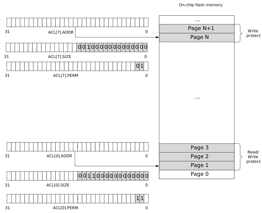
There are four defined ACL permission schemes, each with different combinations of read/write permissions, as shown in the following table.
| Read | Write | Protection description |
|---|---|---|
| 0 | 0 | No protection. Entire region can be executed, read, written to, or erased. |
| 0 | 1 | Region can be executed and read, but not written to or erased. |
| 1 | 0 | Region can be written to and erased, but not executed or read. |
| 1 | 1 | Region is locked for all access until next reset. |
Access control to a configured region is enforced by the hardware. This goes into effect two CPU clock cycles after the ADDR, SIZE, and PERM registers for an ACL instance are written successfully. There are two dependencies for protection to be enforced. First, a valid start address for the flash page boundary must be written to the ADDR register. Second, the SIZE and PERM registers cannot be zero.
The ADDR, SIZE, and PERM registers can only be written once. All ACL configuration registers are cleared on reset by resetting the device from a reset source. This is the only way of clearing the configuration registers. To ensure that the ACL peripheral always enforces the desired permission schemes, the device boot sequence must perform the necessary configuration.
Debugger read access to a read-protected region will be Read-As-Zero (RAZ), while debugger write access to a write-protected region will be Write-Ignored (WI).
Registers
Instances
| Instance | Base address | Description |
|---|---|---|
| ACL | 0x4001E000 | Access control lists |
Register overview
| Register | Offset | Description |
|---|---|---|
| ACL[0].ADDR | 0x800 | Start address of region to protect. The start address must be word-aligned. |
| ACL[0].SIZE | 0x804 | Size of region to protect counting from address ACL[0].ADDR. Writing a '0' has no effect. |
| ACL[0].PERM | 0x808 | Access permissions for region 0 as defined by start address ACL[0].ADDR and size ACL[0].SIZE |
| ACL[1].ADDR | 0x810 | Start address of region to protect. The start address must be word-aligned. |
| ACL[1].SIZE | 0x814 | Size of region to protect counting from address ACL[1].ADDR. Writing a '0' has no effect. |
| ACL[1].PERM | 0x818 | Access permissions for region 1 as defined by start address ACL[1].ADDR and size ACL[1].SIZE |
| ACL[2].ADDR | 0x820 | Start address of region to protect. The start address must be word-aligned. |
| ACL[2].SIZE | 0x824 | Size of region to protect counting from address ACL[2].ADDR. Writing a '0' has no effect. |
| ACL[2].PERM | 0x828 | Access permissions for region 2 as defined by start address ACL[2].ADDR and size ACL[2].SIZE |
| ACL[3].ADDR | 0x830 | Start address of region to protect. The start address must be word-aligned. |
| ACL[3].SIZE | 0x834 | Size of region to protect counting from address ACL[3].ADDR. Writing a '0' has no effect. |
| ACL[3].PERM | 0x838 | Access permissions for region 3 as defined by start address ACL[3].ADDR and size ACL[3].SIZE |
| ACL[4].ADDR | 0x840 | Start address of region to protect. The start address must be word-aligned. |
| ACL[4].SIZE | 0x844 | Size of region to protect counting from address ACL[4].ADDR. Writing a '0' has no effect. |
| ACL[4].PERM | 0x848 | Access permissions for region 4 as defined by start address ACL[4].ADDR and size ACL[4].SIZE |
| ACL[5].ADDR | 0x850 | Start address of region to protect. The start address must be word-aligned. |
| ACL[5].SIZE | 0x854 | Size of region to protect counting from address ACL[5].ADDR. Writing a '0' has no effect. |
| ACL[5].PERM | 0x858 | Access permissions for region 5 as defined by start address ACL[5].ADDR and size ACL[5].SIZE |
| ACL[6].ADDR | 0x860 | Start address of region to protect. The start address must be word-aligned. |
| ACL[6].SIZE | 0x864 | Size of region to protect counting from address ACL[6].ADDR. Writing a '0' has no effect. |
| ACL[6].PERM | 0x868 | Access permissions for region 6 as defined by start address ACL[6].ADDR and size ACL[6].SIZE |
| ACL[7].ADDR | 0x870 | Start address of region to protect. The start address must be word-aligned. |
| ACL[7].SIZE | 0x874 | Size of region to protect counting from address ACL[7].ADDR. Writing a '0' has no effect. |
| ACL[7].PERM | 0x878 | Access permissions for region 7 as defined by start address ACL[7].ADDR and size ACL[7].SIZE |
ACL[0].ADDR
Address offset: 0x800
Start address of region to protect. The start address must be word-aligned.
| Bit number | 31 | 30 | 29 | 28 | 27 | 26 | 25 | 24 | 23 | 22 | 21 | 20 | 19 | 18 | 17 | 16 | 15 | 14 | 13 | 12 | 11 | 10 | 9 | 8 | 7 | 6 | 5 | 4 | 3 | 2 | 1 | 0 | |||
|---|---|---|---|---|---|---|---|---|---|---|---|---|---|---|---|---|---|---|---|---|---|---|---|---|---|---|---|---|---|---|---|---|---|---|---|
| ID | A | A | A | A | A | A | A | A | A | A | A | A | A | A | A | A | A | A | A | A | A | A | A | A | A | A | A | A | A | A | A | A | |||
| Reset 0x00000000 | 0 | 0 | 0 | 0 | 0 | 0 | 0 | 0 | 0 | 0 | 0 | 0 | 0 | 0 | 0 | 0 | 0 | 0 | 0 | 0 | 0 | 0 | 0 | 0 | 0 | 0 | 0 | 0 | 0 | 0 | 0 | 0 | |||
| ID | R/W | Field | Value ID | Value | Description | ||||||||||||||||||||||||||||||
| A | RW1 | ADDR | Start address of flash region 0. The start address must point to a flash page boundary. | ||||||||||||||||||||||||||||||||
ACL[0].SIZE
Address offset: 0x804
Size of region to protect counting from address ACL[0].ADDR. Writing a '0' has no effect.
| Bit number | 31 | 30 | 29 | 28 | 27 | 26 | 25 | 24 | 23 | 22 | 21 | 20 | 19 | 18 | 17 | 16 | 15 | 14 | 13 | 12 | 11 | 10 | 9 | 8 | 7 | 6 | 5 | 4 | 3 | 2 | 1 | 0 | |||
|---|---|---|---|---|---|---|---|---|---|---|---|---|---|---|---|---|---|---|---|---|---|---|---|---|---|---|---|---|---|---|---|---|---|---|---|
| ID | A | A | A | A | A | A | A | A | A | A | A | A | A | A | A | A | A | A | A | A | A | A | A | A | A | A | A | A | A | A | A | A | |||
| Reset 0x00000000 | 0 | 0 | 0 | 0 | 0 | 0 | 0 | 0 | 0 | 0 | 0 | 0 | 0 | 0 | 0 | 0 | 0 | 0 | 0 | 0 | 0 | 0 | 0 | 0 | 0 | 0 | 0 | 0 | 0 | 0 | 0 | 0 | |||
| ID | R/W | Field | Value ID | Value | Description | ||||||||||||||||||||||||||||||
| A | RW1 | SIZE | Size of flash region 0 in bytes. Must be a multiple of the flash page size. | ||||||||||||||||||||||||||||||||
ACL[0].PERM
Address offset: 0x808
Access permissions for region 0 as defined by start address ACL[0].ADDR and size ACL[0].SIZE
| Bit number | 31 | 30 | 29 | 28 | 27 | 26 | 25 | 24 | 23 | 22 | 21 | 20 | 19 | 18 | 17 | 16 | 15 | 14 | 13 | 12 | 11 | 10 | 9 | 8 | 7 | 6 | 5 | 4 | 3 | 2 | 1 | 0 | |||
|---|---|---|---|---|---|---|---|---|---|---|---|---|---|---|---|---|---|---|---|---|---|---|---|---|---|---|---|---|---|---|---|---|---|---|---|
| ID | B | A | |||||||||||||||||||||||||||||||||
| Reset 0x00000000 | 0 | 0 | 0 | 0 | 0 | 0 | 0 | 0 | 0 | 0 | 0 | 0 | 0 | 0 | 0 | 0 | 0 | 0 | 0 | 0 | 0 | 0 | 0 | 0 | 0 | 0 | 0 | 0 | 0 | 0 | 0 | 0 | |||
| ID | R/W | Field | Value ID | Value | Description | ||||||||||||||||||||||||||||||
| A | RW1 | WRITE | Configure write and erase permissions for region 0. Writing a '0' has no effect. | ||||||||||||||||||||||||||||||||
Enable | 0 | Allow write and erase instructions to region 0. | |||||||||||||||||||||||||||||||||
Disable | 1 | Block write and erase instructions to region 0. | |||||||||||||||||||||||||||||||||
| B | RW1 | READ | Configure read permissions for region 0. Writing a '0' has no effect. | ||||||||||||||||||||||||||||||||
Enable | 0 | Allow read instructions to region 0. | |||||||||||||||||||||||||||||||||
Disable | 1 | Block read instructions to region 0. | |||||||||||||||||||||||||||||||||
ACL[1].ADDR
Address offset: 0x810
Start address of region to protect. The start address must be word-aligned.
| Bit number | 31 | 30 | 29 | 28 | 27 | 26 | 25 | 24 | 23 | 22 | 21 | 20 | 19 | 18 | 17 | 16 | 15 | 14 | 13 | 12 | 11 | 10 | 9 | 8 | 7 | 6 | 5 | 4 | 3 | 2 | 1 | 0 | |||
|---|---|---|---|---|---|---|---|---|---|---|---|---|---|---|---|---|---|---|---|---|---|---|---|---|---|---|---|---|---|---|---|---|---|---|---|
| ID | A | A | A | A | A | A | A | A | A | A | A | A | A | A | A | A | A | A | A | A | A | A | A | A | A | A | A | A | A | A | A | A | |||
| Reset 0x00000000 | 0 | 0 | 0 | 0 | 0 | 0 | 0 | 0 | 0 | 0 | 0 | 0 | 0 | 0 | 0 | 0 | 0 | 0 | 0 | 0 | 0 | 0 | 0 | 0 | 0 | 0 | 0 | 0 | 0 | 0 | 0 | 0 | |||
| ID | R/W | Field | Value ID | Value | Description | ||||||||||||||||||||||||||||||
| A | RW1 | ADDR | Start address of flash region 1. The start address must point to a flash page boundary. | ||||||||||||||||||||||||||||||||
ACL[1].SIZE
Address offset: 0x814
Size of region to protect counting from address ACL[1].ADDR. Writing a '0' has no effect.
| Bit number | 31 | 30 | 29 | 28 | 27 | 26 | 25 | 24 | 23 | 22 | 21 | 20 | 19 | 18 | 17 | 16 | 15 | 14 | 13 | 12 | 11 | 10 | 9 | 8 | 7 | 6 | 5 | 4 | 3 | 2 | 1 | 0 | |||
|---|---|---|---|---|---|---|---|---|---|---|---|---|---|---|---|---|---|---|---|---|---|---|---|---|---|---|---|---|---|---|---|---|---|---|---|
| ID | A | A | A | A | A | A | A | A | A | A | A | A | A | A | A | A | A | A | A | A | A | A | A | A | A | A | A | A | A | A | A | A | |||
| Reset 0x00000000 | 0 | 0 | 0 | 0 | 0 | 0 | 0 | 0 | 0 | 0 | 0 | 0 | 0 | 0 | 0 | 0 | 0 | 0 | 0 | 0 | 0 | 0 | 0 | 0 | 0 | 0 | 0 | 0 | 0 | 0 | 0 | 0 | |||
| ID | R/W | Field | Value ID | Value | Description | ||||||||||||||||||||||||||||||
| A | RW1 | SIZE | Size of flash region 1 in bytes. Must be a multiple of the flash page size. | ||||||||||||||||||||||||||||||||
ACL[1].PERM
Address offset: 0x818
Access permissions for region 1 as defined by start address ACL[1].ADDR and size ACL[1].SIZE
| Bit number | 31 | 30 | 29 | 28 | 27 | 26 | 25 | 24 | 23 | 22 | 21 | 20 | 19 | 18 | 17 | 16 | 15 | 14 | 13 | 12 | 11 | 10 | 9 | 8 | 7 | 6 | 5 | 4 | 3 | 2 | 1 | 0 | |||
|---|---|---|---|---|---|---|---|---|---|---|---|---|---|---|---|---|---|---|---|---|---|---|---|---|---|---|---|---|---|---|---|---|---|---|---|
| ID | B | A | |||||||||||||||||||||||||||||||||
| Reset 0x00000000 | 0 | 0 | 0 | 0 | 0 | 0 | 0 | 0 | 0 | 0 | 0 | 0 | 0 | 0 | 0 | 0 | 0 | 0 | 0 | 0 | 0 | 0 | 0 | 0 | 0 | 0 | 0 | 0 | 0 | 0 | 0 | 0 | |||
| ID | R/W | Field | Value ID | Value | Description | ||||||||||||||||||||||||||||||
| A | RW1 | WRITE | Configure write and erase permissions for region 1. Writing a '0' has no effect. | ||||||||||||||||||||||||||||||||
Enable | 0 | Allow write and erase instructions to region 1. | |||||||||||||||||||||||||||||||||
Disable | 1 | Block write and erase instructions to region 1. | |||||||||||||||||||||||||||||||||
| B | RW1 | READ | Configure read permissions for region 1. Writing a '0' has no effect. | ||||||||||||||||||||||||||||||||
Enable | 0 | Allow read instructions to region 1. | |||||||||||||||||||||||||||||||||
Disable | 1 | Block read instructions to region 1. | |||||||||||||||||||||||||||||||||
ACL[2].ADDR
Address offset: 0x820
Start address of region to protect. The start address must be word-aligned.
| Bit number | 31 | 30 | 29 | 28 | 27 | 26 | 25 | 24 | 23 | 22 | 21 | 20 | 19 | 18 | 17 | 16 | 15 | 14 | 13 | 12 | 11 | 10 | 9 | 8 | 7 | 6 | 5 | 4 | 3 | 2 | 1 | 0 | |||
|---|---|---|---|---|---|---|---|---|---|---|---|---|---|---|---|---|---|---|---|---|---|---|---|---|---|---|---|---|---|---|---|---|---|---|---|
| ID | A | A | A | A | A | A | A | A | A | A | A | A | A | A | A | A | A | A | A | A | A | A | A | A | A | A | A | A | A | A | A | A | |||
| Reset 0x00000000 | 0 | 0 | 0 | 0 | 0 | 0 | 0 | 0 | 0 | 0 | 0 | 0 | 0 | 0 | 0 | 0 | 0 | 0 | 0 | 0 | 0 | 0 | 0 | 0 | 0 | 0 | 0 | 0 | 0 | 0 | 0 | 0 | |||
| ID | R/W | Field | Value ID | Value | Description | ||||||||||||||||||||||||||||||
| A | RW1 | ADDR | Start address of flash region 2. The start address must point to a flash page boundary. | ||||||||||||||||||||||||||||||||
ACL[2].SIZE
Address offset: 0x824
Size of region to protect counting from address ACL[2].ADDR. Writing a '0' has no effect.
| Bit number | 31 | 30 | 29 | 28 | 27 | 26 | 25 | 24 | 23 | 22 | 21 | 20 | 19 | 18 | 17 | 16 | 15 | 14 | 13 | 12 | 11 | 10 | 9 | 8 | 7 | 6 | 5 | 4 | 3 | 2 | 1 | 0 | |||
|---|---|---|---|---|---|---|---|---|---|---|---|---|---|---|---|---|---|---|---|---|---|---|---|---|---|---|---|---|---|---|---|---|---|---|---|
| ID | A | A | A | A | A | A | A | A | A | A | A | A | A | A | A | A | A | A | A | A | A | A | A | A | A | A | A | A | A | A | A | A | |||
| Reset 0x00000000 | 0 | 0 | 0 | 0 | 0 | 0 | 0 | 0 | 0 | 0 | 0 | 0 | 0 | 0 | 0 | 0 | 0 | 0 | 0 | 0 | 0 | 0 | 0 | 0 | 0 | 0 | 0 | 0 | 0 | 0 | 0 | 0 | |||
| ID | R/W | Field | Value ID | Value | Description | ||||||||||||||||||||||||||||||
| A | RW1 | SIZE | Size of flash region 2 in bytes. Must be a multiple of the flash page size. | ||||||||||||||||||||||||||||||||
ACL[2].PERM
Address offset: 0x828
Access permissions for region 2 as defined by start address ACL[2].ADDR and size ACL[2].SIZE
| Bit number | 31 | 30 | 29 | 28 | 27 | 26 | 25 | 24 | 23 | 22 | 21 | 20 | 19 | 18 | 17 | 16 | 15 | 14 | 13 | 12 | 11 | 10 | 9 | 8 | 7 | 6 | 5 | 4 | 3 | 2 | 1 | 0 | |||
|---|---|---|---|---|---|---|---|---|---|---|---|---|---|---|---|---|---|---|---|---|---|---|---|---|---|---|---|---|---|---|---|---|---|---|---|
| ID | B | A | |||||||||||||||||||||||||||||||||
| Reset 0x00000000 | 0 | 0 | 0 | 0 | 0 | 0 | 0 | 0 | 0 | 0 | 0 | 0 | 0 | 0 | 0 | 0 | 0 | 0 | 0 | 0 | 0 | 0 | 0 | 0 | 0 | 0 | 0 | 0 | 0 | 0 | 0 | 0 | |||
| ID | R/W | Field | Value ID | Value | Description | ||||||||||||||||||||||||||||||
| A | RW1 | WRITE | Configure write and erase permissions for region 2. Writing a '0' has no effect. | ||||||||||||||||||||||||||||||||
Enable | 0 | Allow write and erase instructions to region 2. | |||||||||||||||||||||||||||||||||
Disable | 1 | Block write and erase instructions to region 2. | |||||||||||||||||||||||||||||||||
| B | RW1 | READ | Configure read permissions for region 2. Writing a '0' has no effect. | ||||||||||||||||||||||||||||||||
Enable | 0 | Allow read instructions to region 2. | |||||||||||||||||||||||||||||||||
Disable | 1 | Block read instructions to region 2. | |||||||||||||||||||||||||||||||||
ACL[3].ADDR
Address offset: 0x830
Start address of region to protect. The start address must be word-aligned.
| Bit number | 31 | 30 | 29 | 28 | 27 | 26 | 25 | 24 | 23 | 22 | 21 | 20 | 19 | 18 | 17 | 16 | 15 | 14 | 13 | 12 | 11 | 10 | 9 | 8 | 7 | 6 | 5 | 4 | 3 | 2 | 1 | 0 | |||
|---|---|---|---|---|---|---|---|---|---|---|---|---|---|---|---|---|---|---|---|---|---|---|---|---|---|---|---|---|---|---|---|---|---|---|---|
| ID | A | A | A | A | A | A | A | A | A | A | A | A | A | A | A | A | A | A | A | A | A | A | A | A | A | A | A | A | A | A | A | A | |||
| Reset 0x00000000 | 0 | 0 | 0 | 0 | 0 | 0 | 0 | 0 | 0 | 0 | 0 | 0 | 0 | 0 | 0 | 0 | 0 | 0 | 0 | 0 | 0 | 0 | 0 | 0 | 0 | 0 | 0 | 0 | 0 | 0 | 0 | 0 | |||
| ID | R/W | Field | Value ID | Value | Description | ||||||||||||||||||||||||||||||
| A | RW1 | ADDR | Start address of flash region 3. The start address must point to a flash page boundary. | ||||||||||||||||||||||||||||||||
ACL[3].SIZE
Address offset: 0x834
Size of region to protect counting from address ACL[3].ADDR. Writing a '0' has no effect.
| Bit number | 31 | 30 | 29 | 28 | 27 | 26 | 25 | 24 | 23 | 22 | 21 | 20 | 19 | 18 | 17 | 16 | 15 | 14 | 13 | 12 | 11 | 10 | 9 | 8 | 7 | 6 | 5 | 4 | 3 | 2 | 1 | 0 | |||
|---|---|---|---|---|---|---|---|---|---|---|---|---|---|---|---|---|---|---|---|---|---|---|---|---|---|---|---|---|---|---|---|---|---|---|---|
| ID | A | A | A | A | A | A | A | A | A | A | A | A | A | A | A | A | A | A | A | A | A | A | A | A | A | A | A | A | A | A | A | A | |||
| Reset 0x00000000 | 0 | 0 | 0 | 0 | 0 | 0 | 0 | 0 | 0 | 0 | 0 | 0 | 0 | 0 | 0 | 0 | 0 | 0 | 0 | 0 | 0 | 0 | 0 | 0 | 0 | 0 | 0 | 0 | 0 | 0 | 0 | 0 | |||
| ID | R/W | Field | Value ID | Value | Description | ||||||||||||||||||||||||||||||
| A | RW1 | SIZE | Size of flash region 3 in bytes. Must be a multiple of the flash page size. | ||||||||||||||||||||||||||||||||
ACL[3].PERM
Address offset: 0x838
Access permissions for region 3 as defined by start address ACL[3].ADDR and size ACL[3].SIZE
| Bit number | 31 | 30 | 29 | 28 | 27 | 26 | 25 | 24 | 23 | 22 | 21 | 20 | 19 | 18 | 17 | 16 | 15 | 14 | 13 | 12 | 11 | 10 | 9 | 8 | 7 | 6 | 5 | 4 | 3 | 2 | 1 | 0 | |||
|---|---|---|---|---|---|---|---|---|---|---|---|---|---|---|---|---|---|---|---|---|---|---|---|---|---|---|---|---|---|---|---|---|---|---|---|
| ID | B | A | |||||||||||||||||||||||||||||||||
| Reset 0x00000000 | 0 | 0 | 0 | 0 | 0 | 0 | 0 | 0 | 0 | 0 | 0 | 0 | 0 | 0 | 0 | 0 | 0 | 0 | 0 | 0 | 0 | 0 | 0 | 0 | 0 | 0 | 0 | 0 | 0 | 0 | 0 | 0 | |||
| ID | R/W | Field | Value ID | Value | Description | ||||||||||||||||||||||||||||||
| A | RW1 | WRITE | Configure write and erase permissions for region 3. Writing a '0' has no effect. | ||||||||||||||||||||||||||||||||
Enable | 0 | Allow write and erase instructions to region 3. | |||||||||||||||||||||||||||||||||
Disable | 1 | Block write and erase instructions to region 3. | |||||||||||||||||||||||||||||||||
| B | RW1 | READ | Configure read permissions for region 3. Writing a '0' has no effect. | ||||||||||||||||||||||||||||||||
Enable | 0 | Allow read instructions to region 3. | |||||||||||||||||||||||||||||||||
Disable | 1 | Block read instructions to region 3. | |||||||||||||||||||||||||||||||||
ACL[4].ADDR
Address offset: 0x840
Start address of region to protect. The start address must be word-aligned.
| Bit number | 31 | 30 | 29 | 28 | 27 | 26 | 25 | 24 | 23 | 22 | 21 | 20 | 19 | 18 | 17 | 16 | 15 | 14 | 13 | 12 | 11 | 10 | 9 | 8 | 7 | 6 | 5 | 4 | 3 | 2 | 1 | 0 | |||
|---|---|---|---|---|---|---|---|---|---|---|---|---|---|---|---|---|---|---|---|---|---|---|---|---|---|---|---|---|---|---|---|---|---|---|---|
| ID | A | A | A | A | A | A | A | A | A | A | A | A | A | A | A | A | A | A | A | A | A | A | A | A | A | A | A | A | A | A | A | A | |||
| Reset 0x00000000 | 0 | 0 | 0 | 0 | 0 | 0 | 0 | 0 | 0 | 0 | 0 | 0 | 0 | 0 | 0 | 0 | 0 | 0 | 0 | 0 | 0 | 0 | 0 | 0 | 0 | 0 | 0 | 0 | 0 | 0 | 0 | 0 | |||
| ID | R/W | Field | Value ID | Value | Description | ||||||||||||||||||||||||||||||
| A | RW1 | ADDR | Start address of flash region 4. The start address must point to a flash page boundary. | ||||||||||||||||||||||||||||||||
ACL[4].SIZE
Address offset: 0x844
Size of region to protect counting from address ACL[4].ADDR. Writing a '0' has no effect.
| Bit number | 31 | 30 | 29 | 28 | 27 | 26 | 25 | 24 | 23 | 22 | 21 | 20 | 19 | 18 | 17 | 16 | 15 | 14 | 13 | 12 | 11 | 10 | 9 | 8 | 7 | 6 | 5 | 4 | 3 | 2 | 1 | 0 | |||
|---|---|---|---|---|---|---|---|---|---|---|---|---|---|---|---|---|---|---|---|---|---|---|---|---|---|---|---|---|---|---|---|---|---|---|---|
| ID | A | A | A | A | A | A | A | A | A | A | A | A | A | A | A | A | A | A | A | A | A | A | A | A | A | A | A | A | A | A | A | A | |||
| Reset 0x00000000 | 0 | 0 | 0 | 0 | 0 | 0 | 0 | 0 | 0 | 0 | 0 | 0 | 0 | 0 | 0 | 0 | 0 | 0 | 0 | 0 | 0 | 0 | 0 | 0 | 0 | 0 | 0 | 0 | 0 | 0 | 0 | 0 | |||
| ID | R/W | Field | Value ID | Value | Description | ||||||||||||||||||||||||||||||
| A | RW1 | SIZE | Size of flash region 4 in bytes. Must be a multiple of the flash page size. | ||||||||||||||||||||||||||||||||
ACL[4].PERM
Address offset: 0x848
Access permissions for region 4 as defined by start address ACL[4].ADDR and size ACL[4].SIZE
| Bit number | 31 | 30 | 29 | 28 | 27 | 26 | 25 | 24 | 23 | 22 | 21 | 20 | 19 | 18 | 17 | 16 | 15 | 14 | 13 | 12 | 11 | 10 | 9 | 8 | 7 | 6 | 5 | 4 | 3 | 2 | 1 | 0 | |||
|---|---|---|---|---|---|---|---|---|---|---|---|---|---|---|---|---|---|---|---|---|---|---|---|---|---|---|---|---|---|---|---|---|---|---|---|
| ID | B | A | |||||||||||||||||||||||||||||||||
| Reset 0x00000000 | 0 | 0 | 0 | 0 | 0 | 0 | 0 | 0 | 0 | 0 | 0 | 0 | 0 | 0 | 0 | 0 | 0 | 0 | 0 | 0 | 0 | 0 | 0 | 0 | 0 | 0 | 0 | 0 | 0 | 0 | 0 | 0 | |||
| ID | R/W | Field | Value ID | Value | Description | ||||||||||||||||||||||||||||||
| A | RW1 | WRITE | Configure write and erase permissions for region 4. Writing a '0' has no effect. | ||||||||||||||||||||||||||||||||
Enable | 0 | Allow write and erase instructions to region 4. | |||||||||||||||||||||||||||||||||
Disable | 1 | Block write and erase instructions to region 4. | |||||||||||||||||||||||||||||||||
| B | RW1 | READ | Configure read permissions for region 4. Writing a '0' has no effect. | ||||||||||||||||||||||||||||||||
Enable | 0 | Allow read instructions to region 4. | |||||||||||||||||||||||||||||||||
Disable | 1 | Block read instructions to region 4. | |||||||||||||||||||||||||||||||||
ACL[5].ADDR
Address offset: 0x850
Start address of region to protect. The start address must be word-aligned.
| Bit number | 31 | 30 | 29 | 28 | 27 | 26 | 25 | 24 | 23 | 22 | 21 | 20 | 19 | 18 | 17 | 16 | 15 | 14 | 13 | 12 | 11 | 10 | 9 | 8 | 7 | 6 | 5 | 4 | 3 | 2 | 1 | 0 | |||
|---|---|---|---|---|---|---|---|---|---|---|---|---|---|---|---|---|---|---|---|---|---|---|---|---|---|---|---|---|---|---|---|---|---|---|---|
| ID | A | A | A | A | A | A | A | A | A | A | A | A | A | A | A | A | A | A | A | A | A | A | A | A | A | A | A | A | A | A | A | A | |||
| Reset 0x00000000 | 0 | 0 | 0 | 0 | 0 | 0 | 0 | 0 | 0 | 0 | 0 | 0 | 0 | 0 | 0 | 0 | 0 | 0 | 0 | 0 | 0 | 0 | 0 | 0 | 0 | 0 | 0 | 0 | 0 | 0 | 0 | 0 | |||
| ID | R/W | Field | Value ID | Value | Description | ||||||||||||||||||||||||||||||
| A | RW1 | ADDR | Start address of flash region 5. The start address must point to a flash page boundary. | ||||||||||||||||||||||||||||||||
ACL[5].SIZE
Address offset: 0x854
Size of region to protect counting from address ACL[5].ADDR. Writing a '0' has no effect.
| Bit number | 31 | 30 | 29 | 28 | 27 | 26 | 25 | 24 | 23 | 22 | 21 | 20 | 19 | 18 | 17 | 16 | 15 | 14 | 13 | 12 | 11 | 10 | 9 | 8 | 7 | 6 | 5 | 4 | 3 | 2 | 1 | 0 | |||
|---|---|---|---|---|---|---|---|---|---|---|---|---|---|---|---|---|---|---|---|---|---|---|---|---|---|---|---|---|---|---|---|---|---|---|---|
| ID | A | A | A | A | A | A | A | A | A | A | A | A | A | A | A | A | A | A | A | A | A | A | A | A | A | A | A | A | A | A | A | A | |||
| Reset 0x00000000 | 0 | 0 | 0 | 0 | 0 | 0 | 0 | 0 | 0 | 0 | 0 | 0 | 0 | 0 | 0 | 0 | 0 | 0 | 0 | 0 | 0 | 0 | 0 | 0 | 0 | 0 | 0 | 0 | 0 | 0 | 0 | 0 | |||
| ID | R/W | Field | Value ID | Value | Description | ||||||||||||||||||||||||||||||
| A | RW1 | SIZE | Size of flash region 5 in bytes. Must be a multiple of the flash page size. | ||||||||||||||||||||||||||||||||
ACL[5].PERM
Address offset: 0x858
Access permissions for region 5 as defined by start address ACL[5].ADDR and size ACL[5].SIZE
| Bit number | 31 | 30 | 29 | 28 | 27 | 26 | 25 | 24 | 23 | 22 | 21 | 20 | 19 | 18 | 17 | 16 | 15 | 14 | 13 | 12 | 11 | 10 | 9 | 8 | 7 | 6 | 5 | 4 | 3 | 2 | 1 | 0 | |||
|---|---|---|---|---|---|---|---|---|---|---|---|---|---|---|---|---|---|---|---|---|---|---|---|---|---|---|---|---|---|---|---|---|---|---|---|
| ID | B | A | |||||||||||||||||||||||||||||||||
| Reset 0x00000000 | 0 | 0 | 0 | 0 | 0 | 0 | 0 | 0 | 0 | 0 | 0 | 0 | 0 | 0 | 0 | 0 | 0 | 0 | 0 | 0 | 0 | 0 | 0 | 0 | 0 | 0 | 0 | 0 | 0 | 0 | 0 | 0 | |||
| ID | R/W | Field | Value ID | Value | Description | ||||||||||||||||||||||||||||||
| A | RW1 | WRITE | Configure write and erase permissions for region 5. Writing a '0' has no effect. | ||||||||||||||||||||||||||||||||
Enable | 0 | Allow write and erase instructions to region 5. | |||||||||||||||||||||||||||||||||
Disable | 1 | Block write and erase instructions to region 5. | |||||||||||||||||||||||||||||||||
| B | RW1 | READ | Configure read permissions for region 5. Writing a '0' has no effect. | ||||||||||||||||||||||||||||||||
Enable | 0 | Allow read instructions to region 5. | |||||||||||||||||||||||||||||||||
Disable | 1 | Block read instructions to region 5. | |||||||||||||||||||||||||||||||||
ACL[6].ADDR
Address offset: 0x860
Start address of region to protect. The start address must be word-aligned.
| Bit number | 31 | 30 | 29 | 28 | 27 | 26 | 25 | 24 | 23 | 22 | 21 | 20 | 19 | 18 | 17 | 16 | 15 | 14 | 13 | 12 | 11 | 10 | 9 | 8 | 7 | 6 | 5 | 4 | 3 | 2 | 1 | 0 | |||
|---|---|---|---|---|---|---|---|---|---|---|---|---|---|---|---|---|---|---|---|---|---|---|---|---|---|---|---|---|---|---|---|---|---|---|---|
| ID | A | A | A | A | A | A | A | A | A | A | A | A | A | A | A | A | A | A | A | A | A | A | A | A | A | A | A | A | A | A | A | A | |||
| Reset 0x00000000 | 0 | 0 | 0 | 0 | 0 | 0 | 0 | 0 | 0 | 0 | 0 | 0 | 0 | 0 | 0 | 0 | 0 | 0 | 0 | 0 | 0 | 0 | 0 | 0 | 0 | 0 | 0 | 0 | 0 | 0 | 0 | 0 | |||
| ID | R/W | Field | Value ID | Value | Description | ||||||||||||||||||||||||||||||
| A | RW1 | ADDR | Start address of flash region 6. The start address must point to a flash page boundary. | ||||||||||||||||||||||||||||||||
ACL[6].SIZE
Address offset: 0x864
Size of region to protect counting from address ACL[6].ADDR. Writing a '0' has no effect.
| Bit number | 31 | 30 | 29 | 28 | 27 | 26 | 25 | 24 | 23 | 22 | 21 | 20 | 19 | 18 | 17 | 16 | 15 | 14 | 13 | 12 | 11 | 10 | 9 | 8 | 7 | 6 | 5 | 4 | 3 | 2 | 1 | 0 | |||
|---|---|---|---|---|---|---|---|---|---|---|---|---|---|---|---|---|---|---|---|---|---|---|---|---|---|---|---|---|---|---|---|---|---|---|---|
| ID | A | A | A | A | A | A | A | A | A | A | A | A | A | A | A | A | A | A | A | A | A | A | A | A | A | A | A | A | A | A | A | A | |||
| Reset 0x00000000 | 0 | 0 | 0 | 0 | 0 | 0 | 0 | 0 | 0 | 0 | 0 | 0 | 0 | 0 | 0 | 0 | 0 | 0 | 0 | 0 | 0 | 0 | 0 | 0 | 0 | 0 | 0 | 0 | 0 | 0 | 0 | 0 | |||
| ID | R/W | Field | Value ID | Value | Description | ||||||||||||||||||||||||||||||
| A | RW1 | SIZE | Size of flash region 6 in bytes. Must be a multiple of the flash page size. | ||||||||||||||||||||||||||||||||
ACL[6].PERM
Address offset: 0x868
Access permissions for region 6 as defined by start address ACL[6].ADDR and size ACL[6].SIZE
| Bit number | 31 | 30 | 29 | 28 | 27 | 26 | 25 | 24 | 23 | 22 | 21 | 20 | 19 | 18 | 17 | 16 | 15 | 14 | 13 | 12 | 11 | 10 | 9 | 8 | 7 | 6 | 5 | 4 | 3 | 2 | 1 | 0 | |||
|---|---|---|---|---|---|---|---|---|---|---|---|---|---|---|---|---|---|---|---|---|---|---|---|---|---|---|---|---|---|---|---|---|---|---|---|
| ID | B | A | |||||||||||||||||||||||||||||||||
| Reset 0x00000000 | 0 | 0 | 0 | 0 | 0 | 0 | 0 | 0 | 0 | 0 | 0 | 0 | 0 | 0 | 0 | 0 | 0 | 0 | 0 | 0 | 0 | 0 | 0 | 0 | 0 | 0 | 0 | 0 | 0 | 0 | 0 | 0 | |||
| ID | R/W | Field | Value ID | Value | Description | ||||||||||||||||||||||||||||||
| A | RW1 | WRITE | Configure write and erase permissions for region 6. Writing a '0' has no effect. | ||||||||||||||||||||||||||||||||
Enable | 0 | Allow write and erase instructions to region 6. | |||||||||||||||||||||||||||||||||
Disable | 1 | Block write and erase instructions to region 6. | |||||||||||||||||||||||||||||||||
| B | RW1 | READ | Configure read permissions for region 6. Writing a '0' has no effect. | ||||||||||||||||||||||||||||||||
Enable | 0 | Allow read instructions to region 6. | |||||||||||||||||||||||||||||||||
Disable | 1 | Block read instructions to region 6. | |||||||||||||||||||||||||||||||||
ACL[7].ADDR
Address offset: 0x870
Start address of region to protect. The start address must be word-aligned.
| Bit number | 31 | 30 | 29 | 28 | 27 | 26 | 25 | 24 | 23 | 22 | 21 | 20 | 19 | 18 | 17 | 16 | 15 | 14 | 13 | 12 | 11 | 10 | 9 | 8 | 7 | 6 | 5 | 4 | 3 | 2 | 1 | 0 | |||
|---|---|---|---|---|---|---|---|---|---|---|---|---|---|---|---|---|---|---|---|---|---|---|---|---|---|---|---|---|---|---|---|---|---|---|---|
| ID | A | A | A | A | A | A | A | A | A | A | A | A | A | A | A | A | A | A | A | A | A | A | A | A | A | A | A | A | A | A | A | A | |||
| Reset 0x00000000 | 0 | 0 | 0 | 0 | 0 | 0 | 0 | 0 | 0 | 0 | 0 | 0 | 0 | 0 | 0 | 0 | 0 | 0 | 0 | 0 | 0 | 0 | 0 | 0 | 0 | 0 | 0 | 0 | 0 | 0 | 0 | 0 | |||
| ID | R/W | Field | Value ID | Value | Description | ||||||||||||||||||||||||||||||
| A | RW1 | ADDR | Start address of flash region 7. The start address must point to a flash page boundary. | ||||||||||||||||||||||||||||||||
ACL[7].SIZE
Address offset: 0x874
Size of region to protect counting from address ACL[7].ADDR. Writing a '0' has no effect.
| Bit number | 31 | 30 | 29 | 28 | 27 | 26 | 25 | 24 | 23 | 22 | 21 | 20 | 19 | 18 | 17 | 16 | 15 | 14 | 13 | 12 | 11 | 10 | 9 | 8 | 7 | 6 | 5 | 4 | 3 | 2 | 1 | 0 | |||
|---|---|---|---|---|---|---|---|---|---|---|---|---|---|---|---|---|---|---|---|---|---|---|---|---|---|---|---|---|---|---|---|---|---|---|---|
| ID | A | A | A | A | A | A | A | A | A | A | A | A | A | A | A | A | A | A | A | A | A | A | A | A | A | A | A | A | A | A | A | A | |||
| Reset 0x00000000 | 0 | 0 | 0 | 0 | 0 | 0 | 0 | 0 | 0 | 0 | 0 | 0 | 0 | 0 | 0 | 0 | 0 | 0 | 0 | 0 | 0 | 0 | 0 | 0 | 0 | 0 | 0 | 0 | 0 | 0 | 0 | 0 | |||
| ID | R/W | Field | Value ID | Value | Description | ||||||||||||||||||||||||||||||
| A | RW1 | SIZE | Size of flash region 7 in bytes. Must be a multiple of the flash page size. | ||||||||||||||||||||||||||||||||
ACL[7].PERM
Address offset: 0x878
Access permissions for region 7 as defined by start address ACL[7].ADDR and size ACL[7].SIZE
| Bit number | 31 | 30 | 29 | 28 | 27 | 26 | 25 | 24 | 23 | 22 | 21 | 20 | 19 | 18 | 17 | 16 | 15 | 14 | 13 | 12 | 11 | 10 | 9 | 8 | 7 | 6 | 5 | 4 | 3 | 2 | 1 | 0 | |||
|---|---|---|---|---|---|---|---|---|---|---|---|---|---|---|---|---|---|---|---|---|---|---|---|---|---|---|---|---|---|---|---|---|---|---|---|
| ID | B | A | |||||||||||||||||||||||||||||||||
| Reset 0x00000000 | 0 | 0 | 0 | 0 | 0 | 0 | 0 | 0 | 0 | 0 | 0 | 0 | 0 | 0 | 0 | 0 | 0 | 0 | 0 | 0 | 0 | 0 | 0 | 0 | 0 | 0 | 0 | 0 | 0 | 0 | 0 | 0 | |||
| ID | R/W | Field | Value ID | Value | Description | ||||||||||||||||||||||||||||||
| A | RW1 | WRITE | Configure write and erase permissions for region 7. Writing a '0' has no effect. | ||||||||||||||||||||||||||||||||
Enable | 0 | Allow write and erase instructions to region 7. | |||||||||||||||||||||||||||||||||
Disable | 1 | Block write and erase instructions to region 7. | |||||||||||||||||||||||||||||||||
| B | RW1 | READ | Configure read permissions for region 7. Writing a '0' has no effect. | ||||||||||||||||||||||||||||||||
Enable | 0 | Allow read instructions to region 7. | |||||||||||||||||||||||||||||||||
Disable | 1 | Block read instructions to region 7. | |||||||||||||||||||||||||||||||||