Pin assignments
The pin assignment figures and tables describe the pinouts for the product variants of the chip.
The nRF52820 device provides flexibility regarding GPIO pin routing and configuration. However, some pins have limitations or recommendations for pin configurations and uses.
QFN40 pin assignments
The pin assignment figure and table describe the assignments for this variant of the chip.
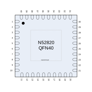
| Pin | Name | Function | Description | Recommended usage |
|---|---|---|---|---|
| Left side of the chip | ||||
| 1 | DEC1 | Power | 1.1 V Digital supply decoupling | |
| 2 | P0.00 XL1 | Digital I/O Analog input | General purpose I/O Connection for 32.768 kHz crystal | |
| 3 | P0.01 XL2 | Digital I/O Analog input | General purpose I/O Connection for 32.768 kHz crystal | |
| 4 | P0.04 AIN2 | Digital I/O Analog input | General purpose I/O Analog input | |
| 5 | P0.05 AIN3 | Digital I/O Analog input | General purpose I/O Analog input | |
| 6 | P0.06 | Digital I/O | General purpose I/O | |
| 7 | P0.07 | Digital I/O | General purpose I/O | |
| 8 | VDD | Power | Power supply | |
| 9 | VDDH | Power | High voltage power supply | |
| 10 | VBUS | Power | 5 V input for USB 3.3 V regulator | |
| Bottom side of the chip | ||||
| 11 | DECUSB | Power | USB 3.3 V regulator supply decoupling | |
| 12 | D- | USB | USB D- | |
| 13 | D+ | USB | USB D+ | |
| 14 | P0.14 | Digital I/O | General purpose I/O | |
| 15 | P0.15 | Digital I/O | General purpose I/O | |
| 16 | P0.18 nRESET | Digital I/O | General purpose I/O Configurable as pin RESET | |
| 17 | P0.20 | Digital I/O | General purpose I/O | |
| 18 | VDD | Power | Power supply | |
| 19 | SWDIO | Debug | Serial wire debug I/O for debug and programming | |
| 20 | SWDCLK | Debug | Serial wire debug clock input for debug and programming | |
| Right side of the chip | ||||
| 21 | DEC5 Not connected | Power | 1.3 V regulator supply decoupling for build codes Cxx and earlier. Not connected for build codes Dxx and later. | |
| 22 | P0.16 | Digital I/O | General purpose I/O | Standard drive, low frequency I/O only |
| 23 | P0.17 | Digital I/O | General purpose I/O | Standard drive, low frequency I/O only |
| 24 | ANT | RF | Single-ended radio antenna connection | See Reference circuitry for guidelines on how to ensure good RF performance |
| 25 | VSS_PA | Power | Ground (radio supply) | |
| 26 | DEC6 | Power | 1.3 V regulator supply decoupling | Must be connected to DEC4 (pin 38) |
| 27 | DEC3 | Power | Power supply, decoupling | |
| 28 | XC1 | Analog input | Connection for 32 MHz crystal | |
| 29 | XC2 | Analog input | Connection for 32 MHz crystal | |
| 30 | VDD | Power | Power supply | |
| Top side of the chip | ||||
| 31 | P0.08 | Digital I/O | General purpose I/O | Standard drive, low frequency I/O only |
| 32 | P0.29 | Digital I/O | General purpose I/O | Standard drive, low frequency I/O only |
| 33 | P0.30 | Digital I/O | General purpose I/O | Standard drive, low frequency I/O only |
| 34 | P0.28 | Digital I/O | General purpose I/O | Standard drive, low frequency I/O only |
| 35 | P0.03 AIN1 | Digital I/O Analog input | General purpose I/O Analog input | Standard drive, low frequency I/O only |
| 36 | P0.02 AIN0 | Digital I/O Analog input | General purpose I/O Analog input | |
| 37 | VSS | Power | Ground | |
| 38 | DEC4 | Power | 1.3 V regulator supply decoupling | Must be connected to DEC6 (pin 26) |
| 39 | DCC | Power | DC/DC converter output | |
| 40 | VDD | Power | Power supply | |
| Backside of the the chip | ||||
| Die pad | VSS | Power | Ground pad | Exposed die pad must be connected to ground (VSS) for proper device operation |
For more information on standard drive, see GPIO — General purpose input/output. Low frequency I/O is a signal with a frequency up to 10 kHz.
WLCSP ball assignments
The ball assignment figure and table describe the assignments for this variant of the chip.
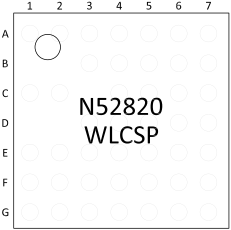
| Pin | Name | Function | Description | Recommended usage |
|---|---|---|---|---|
| A1 | XC1 | Analog input | Connection for 32 MHz crystal | |
| A2 | XC2 | Analog input | Connection for 32 MHz crystal | |
| A3 | VDD | Power | Power supply | |
| A4 | VSS | Power | Ground | |
| A5 | DEC4 | Power | 1.3 V regulator supply decoupling | Must be connected to DEC6 (ball C2) |
| A6 | DCC | Power | DC/DC converter output | |
| A7 | DEC1 | Power | 1.1 V Digital supply decoupling | |
| B3 | P0.08 | Digital I/O | General purpose I/O | Standard drive, low frequency I/O only |
| B4 | P0.30 | Digital I/O | General purpose I/O | Standard drive, low frequency I/O only |
| B5 | P0.03 AIN1 | Digital I/O Analog input | General purpose I/O pin Analog input | Standard drive, low frequency I/O only |
| B6 | P0.02 AIN0 | Digital I/O Analog input | General purpose I/O pin Analog input | |
| B7 | VDD | Power | Power supply | |
| C1 | VSS_PA | Power | Ground (radio supply) | |
| C2 | DEC6 | Power | 1.3 V regulator supply decoupling | Must be connected to DEC4 (ball A5) |
| C4 | P0.29 | Digital I/O | General purpose I/O | Standard drive, low frequency I/O only |
| C5 | P0.28 | Digital I/O | General purpose I/O | Standard drive, low frequency I/O only |
| C6 | P0.04 AIN2 | Digital I/O Analog input | General purpose I/O pin Analog input | |
| C7 | P0.00 XL1 | Digital I/O Analog input | General purpose I/O pin Connection for 32.768 kHz crystal | |
| D3 | VSS | Power | Ground | |
| D4 | VSS | Power | Ground | |
| D5 | VSS | Power | Ground | |
| D6 | P0.05 AIN3 | Digital I/O Analog input | General purpose I/O pin Analog input | |
| D7 | P0.01 XL2 | Digital I/O Analog input | General purpose I/O pin Connection for 32.768 kHz crystal | |
| E1 | ANT | RF | Single-ended radio antenna connection | See Reference circuitry for guidelines on how to ensure good RF performance |
| E2 | P0.17 | Digital I/O | General purpose I/O | Standard drive, low frequency I/O only |
| E3 | P0.16 | Digital I/O | General purpose I/O | Standard drive, low frequency I/O only |
| E4 | VSS | Power | Ground | |
| E5 | VSS | Power | Ground | |
| E6 | P0.06 | Digital I/O | General purpose I/O | |
| E7 | VDD | Power | Power supply | |
| F1 | DEC5 Not connected | Power | 1.3 V regulator supply decoupling for build codes Cxx and earlier. Not connected for build codes Dxx and later. | |
| F2 | P0.20 | Digital I/O | General purpose I/O | Standard drive, low frequency I/O only |
| F3 | P0.15 | Digital I/O | General purpose I/O | Standard drive, low frequency I/O only |
| F4 | P0.14 | Digital I/O | General purpose I/O | |
| F5 | VSS | Power | Ground | |
| F6 | P0.07 | Digital I/O | General purpose I/O | |
| F7 | VDDH | Power | High voltage power supply | |
| G1 | SWDIO | Debug | Serial wire debug I/O for debug and programming | |
| G2 | SWDCLK | Debug | Serial wire debug clock input for debug and programming | |
| G3 | P0.18 nRESET | Digital I/O | General purpose I/O Configurable as pin RESET | |
| G4 | D- | USB | USB D- | |
| G5 | D+ | USB | USB D+ | |
| G6 | DECUSB | Power | USB 3.3 V regulator supply decoupling | |
| G7 | VBUS | Power | 5 V input for USB 3.3 V regulator |
For more information on standard drive, see GPIO — General purpose input/output. Low frequency I/O is a signal with a frequency up to 10 kHz.