Pin assignments
Here we cover the pin assignments for each variant of the chip.
QFN48 pin assignments
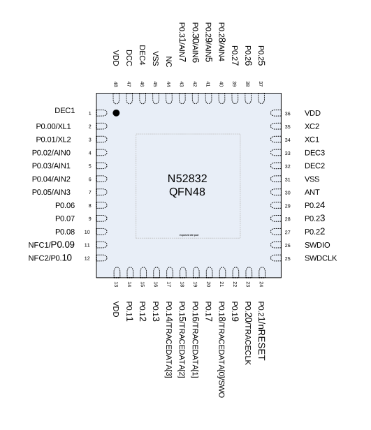
| Pin | Name | Type | Description |
|---|---|---|---|
| Left Side of chip | |||
| 1 | DEC1 | Power | 0.9 V regulator digital supply decoupling |
| 2 | P0.00 XL1 | Digital I/O Analog input | General purpose I/O Connection for 32.768 kHz crystal (LFXO) |
| 3 | P0.01 XL2 | Digital I/O Analog input | General purpose I/O Connection for 32.768 kHz crystal (LFXO) |
| 4 | P0.02 AIN0 | Digital I/O Analog input | General purpose I/O SAADC/COMP/LPCOMP input |
| 5 | P0.03 AIN1 | Digital I/O Analog input | General purpose I/O SAADC/COMP/LPCOMP input |
| 6 | P0.04 AIN2 | Digital I/O Analog input | General purpose I/O SAADC/COMP/LPCOMP input |
| 7 | P0.05 AIN3 | Digital I/O Analog input | General purpose I/O SAADC/COMP/LPCOMP input |
| 8 | P0.06 | Digital I/O | General purpose I/O |
| 9 | P0.07 | Digital I/O | General purpose I/O |
| 10 | P0.08 | Digital I/O | General purpose I/O |
11 | NFC1 P0.09 | NFC input Digital I/O | NFC antenna connection General purpose I/O. |
12 | NFC2 P0.10 | NFC input Digital I/O | NFC antenna connection General purpose I/O. |
| Bottom side of chip | |||
| 13 | VDD | Power | Power supply |
| 14 | P0.11 | Digital I/O | General purpose I/O |
| 15 | P0.12 | Digital I/O | General purpose I/O |
| 16 | P0.13 | Digital I/O | General purpose I/O |
| 17 | P0.14 TRACEDATA[3] | Digital I/O | General purpose I/O Trace port output |
| 18 | P0.15 TRACEDATA[2] | Digital I/O | General purpose I/O Trace port output |
| 19 | P0.16 TRACEDATA[1] | Digital I/O | General purpose I/O Trace port output |
| 20 | P0.17 | Digital I/O | General purpose I/O |
| 21 | P0.18 TRACEDATA[0] / SWO | Digital I/O | General purpose I/O Single wire output Trace port output |
| 22 | P0.19 | Digital I/O | General purpose I/O |
| 23 | P0.20 TRACECLK | Digital I/O | General purpose I/O Trace port clock output |
| 24 | P0.21 nRESET | Digital I/O | General purpose I/O Configurable as pin reset |
| Right Side of chip | |||
| 25 | SWDCLK | Digital input | Serial wire debug clock input for debug and programming |
| 26 | SWDIO | Digital I/O | Serial wire debug I/O for debug and programming |
| 27 | P0.22 | Digital I/O | General purpose I/O. |
| 28 | P0.23 | Digital I/O | General purpose I/O. |
| 29 | P0.24 | Digital I/O | General purpose I/O. |
| 30 | ANT | RF | Single-ended radio antenna connection |
| 31 | VSS | Power | Ground (Radio supply) |
| 32 | DEC2 | Power | 1.3 V regulator supply decoupling (Radio supply) |
| 33 | DEC3 | Power | Power supply decoupling |
| 34 | XC1 | Analog input | Connection for 32 MHz crystal |
| 35 | XC2 | Analog input | Connection for 32 MHz crystal |
| 36 | VDD | Power | Power supply |
| Top side of chip | |||
| 37 | P0.25 | Digital I/O | General purpose I/O. |
| 38 | P0.26 | Digital I/O | General purpose I/O. |
| 39 | P0.27 | Digital I/O | General purpose I/O. |
| 40 | P0.28 AIN4 | Digital I/O Analog input | General purpose I/O. SAADC/COMP/LPCOMP input |
| 41 | P0.29 AIN5 | Digital I/O Analog input | General purpose I/O. SAADC/COMP/LPCOMP input |
| 42 | P0.30 AIN6 | Digital I/O Analog input | General purpose I/O. SAADC/COMP/LPCOMP input |
| 43 | P0.31 AIN7 | Digital I/O Analog input | General purpose I/O pin. SAADC/COMP/LPCOMP input |
| 44 | NC | No connect Leave unconnected | |
| 45 | VSS | Power | Ground |
| 46 | DEC4 | Power | 1.3 V regulator supply decoupling Input from DC/DC regulator Output from 1.3 V LDO |
| 47 | DCC | Power | DC/DC regulator output |
| 48 | VDD | Power | Power supply |
| Bottom of chip | |||
| Die pad | VSS | Power | Ground pad Exposed die pad must be connected to ground (VSS) for proper device operation. |
WLCSP ball assignments
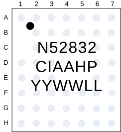
| Ball | Name | Description | |
|---|---|---|---|
| A1 | XC2 | Analog input | Connection for 32 MHz crystal |
| A2 | DEC2 | Power | 1.3 V regulator supply decoupling (Radio supply) |
| A3 | P0.28 AIN4 | Digital I/O Analog input | General purpose I/O. SAADC/COMP/LPCOMP input |
| A4 | P0.29 AIN5 | Digital I/O Analog input | General purpose I/O. SAADC/COMP/LPCOMP input |
| A5 | P0.30 AIN6 | Digital I/O Analog input | General purpose I/O. SAADC/COMP/LPCOMP input |
| A6 | DEC4 | Power | 1.3 V regulator supply decoupling Input from DC/DC converter. Output from 1.3 V LDO |
| A7 | VDD | Power | Power supply |
| B2 | XC1 | Analog input | Connection for 32 MHz crystal |
| B3 | P0.25 | Digital I/O | General purpose I/O. |
| B4 | P0.27 | Digital I/O | General purpose I/O. |
| B5 | P0.31 AIN7 | Digital I/O Analog input | General purpose I/O. SAADC/COMP/LPCOMP input |
| B6 | DCC | Power | DC/DC converter output |
| B7 | DEC1 | Power | 0.9 V regulator digital supply decoupling |
| C2 | DEC3 | Power | Power supply decoupling |
| C3 | NC | N/A | Not connected |
| C4 | VSS | Power | Ground |
| C5 | VSS | Power | Ground |
| C6 | P0.02 AIN0 | Digital I/O Analog input | General purpose I/O SAADC/COMP/LPCOMP input |
| C7 | P0.01 XL2 | Digital I/O Analog input | General purpose I/O Connection for 32.768 kHz crystal (LFXO) |
| D1 | ANT | RF | Single-ended radio antenna connection |
| D2 | VSS_PA | Power | Ground (Radio supply) |
| D3 | P0.26 | Digital I/O | General purpose I/O . |
| D6 | P0.03 AIN1 | Digital I/O Analog input | General purpose I/O SAADC/COMP/LPCOMP input |
| D7 | P0.00 XL1 | Digital I/O Analog input | General purpose I/O Connection for 32.768 kHz crystal (LFXO) |
| E1 | P0.24 | Digital I/O | General purpose I/O. |
| E2 | P0.23 | Digital I/O | General purpose I/O. |
| E3 | VSS | Power | Ground |
| E6 | P0.04 AIN2 | Digital I/O Analog input | General purpose I/O SAADC/COMP/LPCOMP input |
| E7 | P0.05 AIN3 | Digital I/O Analog input | General purpose I/O SAADC/COMP/LPCOMP input |
| F1 | SWDCLK | Digital input | Serial wire debug clock input for debug and programming |
| F2 | P0.22 | Digital I/O | General purpose I/O. |
| F3 | P0.19 | Digital I/O | General purpose I/O |
| F4 | P0.11 | Digital I/O | General purpose I/O |
| F5 | VSS | Power | Ground |
| F6 | P0.07 | Digital I/O | General purpose I/O |
| F7 | P0.06 | Digital I/O | General purpose I/O |
| G1 | SWDIO | Digital I/O | Serial wire debug I/O for debug and programming |
| G2 | P0.20 TRACECLK | Digital I/O | General purpose I/O Trace port clock output |
| G3 | P0.17 | Digital I/O | General purpose I/O |
| G4 | P0.13 | Digital I/O | General purpose I/O |
| G5 | NFC2 P0.10 | NFC input Digital I/O | NFC antenna connection General purpose I/O. |
| G6 | NFC1 P0.09 | NFC input Digital I/O | NFC antenna connection General purpose I/O. |
| G7 | P0.08 | Digital I/O | General purpose I/O |
| H1 | P0.21 nRESET | Digital I/O | General purpose I/O Configurable as pin reset |
| H2 | P0.18 TRACEDATA[0] | Digital I/O | General purpose I/O Trace port output |
| H3 | P0.16 TRACEDATA[1] | Digital I/O | General purpose I/O Trace port output |
| H4 | P0.15 TRACEDATA[2] | Digital I/O | General purpose I/O Trace port output |
| H5 | P0.14 TRACEDATA[3] | Digital I/O | General purpose I/O Trace port output |
| H6 | P0.12 | Digital I/O | General purpose I/O |
| H7 | VDD | Power | Power supply |
GPIO usage restrictions
For more information on standard drive, see GPIO — General purpose input/output. Low frequency I/O is a signal with a frequency up to 10 kHz.
GPIO located near the radio
Radio performance parameters, such as sensitivity, may be affected by high frequency digital I/O with large sink/source current close to the Radio power supply and antenna pins.
Table 3 and Table 4 identify some GPIO that have recommended usage guidelines to maximize radio performance in an application.
| Pin | GPIO | Recommended usage |
|---|---|---|
| 27 | P0.22 | Low drive, low frequency I/O only. |
| 28 | P0.23 | |
| 29 | P0.24 | |
| 37 | P0.25 | |
| 38 | P0.26 | |
| 39 | P0.27 | |
| 40 | P0.28 | |
| 41 | P0.29 | |
| 42 | P0.30 | |
| 43 | P0.31 |
| Pin | GPIO | Recommended usage |
|---|---|---|
| F2 | P0.22 | Low drive, low frequency I/O only. |
| E2 | P0.23 | |
| E1 | P0.24 | |
| B3 | P0.25 | |
| D3 | P0.26 | |
| B4 | P0.27 | |
| A3 | P0.28 | |
| A4 | P0.29 | |
| A5 | P0.30 | |
| B5 | P0.31 |
NFC antenna pins
Two physical pins can be configured either as NFC antenna pins (factory default), or as GPIOs, as shown below.
| NFC pad name | GPIO |
|---|---|
| NFC1 | P0.09 |
| NFC2 | P0.10 |
When configured as NFC antenna pins, the GPIOs on those pins will automatically be set to DISABLE state and a protection circuit will be enabled preventing the chip from being damaged in the presence of a strong NFC field. The protection circuit will short the two pins together if voltage difference exceeds approximately 2 V.
For information on how to configure these pins as normal GPIOs, see NFCT — Near field communication tag and UICR — User information configuration registers. Note that the device will not be protected against strong NFC field damage if the pins are configured as GPIO and an NFC antenna is connected to the device. The pins will always be configured as NFC pins during power-on reset until the configuration is set according to the UICR register.
These two pins will have some limitations when configured as GPIO. The pin capacitance will be higher on these pins, and there is some current leakage between the two pins if they are driven to different logical values. To avoid leakage between the pins when configured as GPIO, these GPIOs should always be at the same logical value whenever entering one of the device power saving modes. See Electrical specification.