RADIO — 2.4 GHz Radio
The RADIO contains a 2.4 GHz radio receiver and a 2.4 GHz radio transmitter that is compatible with Nordic's proprietary 1 Mbps and 2 Mbps radio modes in addition to 1 Mbps and 2 Mbps Bluetooth® low energy mode.
EasyDMA in combination with an automated packet assembler and packet disassembler, and an automated CRC generator and CRC checker, makes it very easy to configure and use the RADIO. See Figure 1 for details.
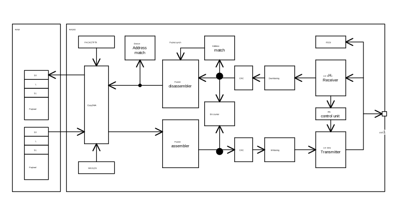
The RADIO includes a Device Address Match unit and an interframe spacing control unit that can be utilized to simplify address white listing and interframe spacing respectively, in Bluetooth Smart and similar applications.
The RADIO also includes a Received Signal Strength Indicator (RSSI) and a bit counter. The bit counter generates events when a preconfigured number of bits have been sent or received by the RADIO.
EasyDMA
The RADIO use EasyDMA for reading and writing of data packets from and to the RAM without CPU involvement.
As illustrated in Figure 1, the RADIO's EasyDMA utilizes the same PACKETPTR for receiving and transmitting packets. The CPU should reconfigure this pointer every time before the RADIO is started via the START task.
The structure of a radio packet is described in detail in Packet configuration. The data that is stored in Data RAM and transported by EasyDMA consists of S0, LENGTH, S1, the payload itself, and a static add-on sent immediately after the payload.
The size of each of the above elements in the frame is configurable (see Packet configuration), and the space occupied in RAM depends on these settings. A size of zero is possible for any of the fields, it is up to the user to make sure that the resulting frame complies with the RF protocol chosen.
For the field sizes defined in bits, the occupation in RAM will always be rounded up to the next full byte size (for instance 3 bit length will allocate 1 byte in RAM, 9 bit length will allocate 2 bytes, etc.).
In addition, the S0INCL field in PCNF0 determines if S0 is present in RAM at all if its length is zero. If present, one byte is allocated in RAM.
The size of S0 is configured through the S0LEN field in PCNF0. The size of LENGTH is configured through the LFLEN field in PCNF0. The size of S1 is configured through the S1LEN field in PCNF0. The size of the payload is configured through the value in RAM corresponding to the LENGTH field. The size of the static add-on to the payload is configured through the STATLEN field in PCNF1.
The MAXLEN field in the PCNF1 register configures the maximum packet payload plus add-on size in number of bytes that can be transmitted or received by the RADIO. This feature can be used to ensure that the RADIO does not overwrite, or read beyond, the RAM assigned to the packet payload. This means that if the packet payload length defined by PCNF1.STATLEN and the LENGTH field in the packet specifies a packet larger than MAXLEN, the payload will be truncated at MAXLEN.
Note that MAXLEN includes the payload and the add-on, but excludes the size occupied by the S0, LENGTH and S1 fields. This has to be taken into account when allocating RAM.
If the payload plus add-on length is specified larger than MAXLEN, the RADIO will still transmit or receive in the same way as before except the payload is now truncated to MAXLEN. The packet's LENGTH field will not be altered when the payload is truncated. The RADIO will calculate CRC as if the packet length is equal to MAXLEN.
If the PACKETPTR is not pointing to the Data RAM region, an EasyDMA transfer may result in a HardFault or RAM corruption. See Memory for more information about the different memory regions.
The DISABLED event indicates that the EasyDMA has finished accessing the RAM.
Packet configuration
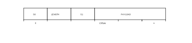
A Radio packet contains the following fields: PREAMBLE, ADDRESS, S0, LENGTH, S1, PAYLOAD and CRC.
See Figure 2. Not shown in the figure is the static payload add-on (the length of which is defined in STATLEN, and which is 0 bytes long in a standard BLE packet), and would be sent between PAYLOAD and CRC. The Radio sends the different fields in the packet in the order they are illustrated below, from left to right. The preamble will be sent least significant bit first on-air.

For all modes, except for 2 Mbit/s Bluetooth Low Energy mode, the preamble is one byte long. For 2 Mbit/s Bluetooth Low Energy mode the preamble is 2 bytes long. If the first bit of the ADDRESS is 0 the preamble will be set to 0xAA otherwise the PREAMBLE will be set to 0x55.
Radio packets are stored in memory inside instances of a radio packet data structure as illustrated in Figure 3. The PREAMBLE, ADDRESS and CRC fields are omitted in this data structure.
The byte ordering on air is always Least Significant Byte First for the ADDRESS and PAYLOAD fields and Most Significant Byte First for the CRC field. The ADDRESS fields are always transmitted and received least significant bit first on-air. The CRC field is always transmitted and received Most Significant Bit first. The bit-endian, i.e. which order the bits are sent and received in, of the S0, LENGTH, S1 and PAYLOAD fields can be configured via the ENDIAN in PCNF1.
The S0INCL field in PCNF0 determines if S0 is present in RAM at all if its length is zero. If present, one byte is allocated in RAM.
The sizes of the S0, LENGTH and S1 fields can be individually configured via S0LEN, LFLEN and S1LEN in PCNF0 respectively. If any of these fields are configured to be less than 8 bit long the, the least significant bits of the fields, as seen from the RAM representation, are used.
If S0, LENGTH or S1 are specified with zero length their fields will be omitted in memory, otherwise each field will be represented as a separate byte, regardless of the number of bits in their on-air counterpart.
Maximum packet length
Independent of the configuration of MAXLEN, the combined length of S0, LENGTH, S1 and PAYLOAD cannot exceed 258 bytes.
Address configuration
The on-air radio ADDRESS field is composed of two parts, the base address field and the address prefix field.
The size of the base address field is configurable via BALEN in PCNF1. The base address is truncated from LSByte if the BALEN is less than 4. See Table 1.
The on-air addresses are defined in the BASEn and PREFIXn registers, and it is only when writing these registers the user will have to relate to actual on-air addresses. For other radio address registers such as the TXADDRESS, RXADDRESSES and RXMATCH registers, logical radio addresses ranging from 0 to 7 are being used. The relationship between the on-air radio addresses and the logical addresses is described in Table 1.
| Logical address | Base address | Prefix byte |
|---|---|---|
| 0 | BASE0 | PREFIX0.AP0 |
| 1 | BASE1 | PREFIX0.AP1 |
| 2 | BASE1 | PREFIX0.AP2 |
| 3 | BASE1 | PREFIX0.AP3 |
| 4 | BASE1 | PREFIX1.AP4 |
| 5 | BASE1 | PREFIX1.AP5 |
| 6 | BASE1 | PREFIX1.AP6 |
| 7 | BASE1 | PREFIX1.AP7 |
Data whitening
The RADIO is able to do packet whitening and de-whitening.
See WHITEEN in PCNF1 register for how to enable whitening. When enabled, whitening and de-whitening will be handled by the RADIO automatically as packets are sent and received.
The whitening word is generated using polynomial g(D) = D7+ D4 + 1, which then is XORed with the data packet that is to be whitened, or de-whitened. See the figure below.
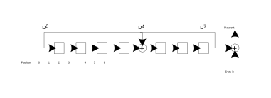
Whitening and de-whitening will be performed over the whole packet (except for the preamble and the address field).
The linear feedback shift register, illustrated in Figure 4 can be initialised via the DATAWHITEIV register.
CRC
The CRC generator in the RADIO calculates the CRC over the whole packet excluding the preamble. If desirable, the address field can be excluded from the CRC calculation as well
See CRCCNF register for more information.
The CRC polynomial is configurable as illustrated in Figure 5 where bit 0 in the CRCPOLY register corresponds to X0 and bit 1 corresponds to X1 etc. See CRCPOLY for more information.
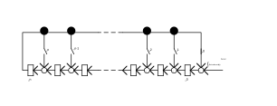
As illustrated in Figure 5, the CRC is calculated by feeding the packet serially through the CRC generator. Before the packet is clocked through the CRC generator, the CRC generator's latches b0 through bn will be initialized with a predefined value specified in the CRCINIT register. When the whole packet is clocked through the CRC generator, latches b0 through bn will hold the resulting CRC. This value will be used by the RADIO during both transmission and reception but it is not available to be read by the CPU at any time. A received CRC can however be read by the CPU via the RXCRC register independent of whether or not it has passed the CRC check.
The length (n) of the CRC is configurable, see CRCCNF for more information.
After the whole packet including the CRC has been received, the RADIO will generate a CRCOK event if no CRC errors were detected, or alternatively generate a CRCERROR event if CRC errors were detected.
The status of the CRC check can be read from the CRCSTATUS register after a packet has been received.
Radio states
The RADIO can enter a number of states.
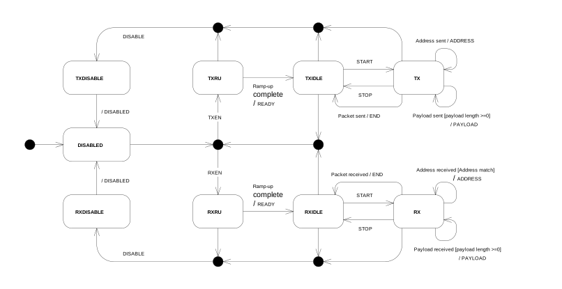
The RADIO can enter the states described the table below. An overview state diagram for the RADIO is illustrated in Figure 6. This figure shows how the tasks and events relate to the RADIO's operation. The RADIO does not prevent a task from being triggered from the wrong state. If a task is triggered from the wrong state, for example if the RXEN task is triggered from the RXDISABLE state, this may lead to incorrect behaviour. As illustrated in Figure 6, the PAYLOAD event is always generated even if the payload is zero.
| State | Description |
|---|---|
| DISABLED | No operations are going on inside the radio and the power consumption is at a minimum |
| RXRU | The radio is ramping up and preparing for reception |
| RXIDLE | The radio is ready for reception to start |
| RX | Reception has been started and the addresses enabled in the RXADDRESSES register are being monitored |
| TXRU | The radio is ramping up and preparing for transmission |
| TXIDLE | The radio is ready for transmission to start |
| TX | The radio is transmitting a packet |
| RXDISABLE | The radio is disabling the receiver |
| TXDISABLE | The radio is disabling the transmitter |
Transmit sequence
Before the RADIO is able to transmit a packet, it must first ramp-up in TX mode.
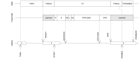
See TXRU in Figure 6 and Figure 7. A TXRU ramp-up sequence is initiated when the TXEN task is triggered. After the radio has successfully ramped up it will generate the READY event indicating that a packet transmission can be initiate. A packet transmission is initiated by triggering the START task. As illustrated in Figure 6 the START task can first be triggered after the RADIO has entered into the TXIDLE state.
Figure 7 illustrates a single packet transmission where the CPU manually triggers the different tasks needed to control the flow of the RADIO, i.e. no shortcuts are used. If shortcuts are not used, a certain amount of delay caused by CPU execution is expected between READY and START, and between END and DISABLE. As illustrated in Figure 7 the RADIO will by default transmit '1's between READY and START, and between END and DISABLED. What is transmitted can be programmed through the DTX field in the MODECNF0 register.
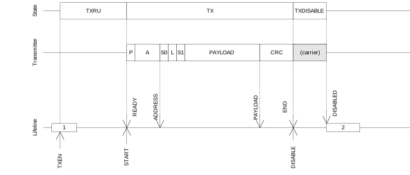
A slightly modified version of the transmit sequence from Figure 7 is illustrated in Figure 8 where the RADIO is configured to use shortcuts between READY and START, and between END and DISABLE, which means that no delay is introduced.
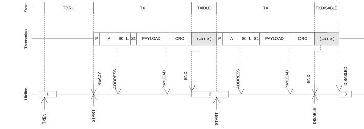
The RADIO is able to send multiple packets one after the other without having to disable and re-enable the RADIO between packets, this is illustrated in Figure 9.
Receive sequence
Before the RADIO is able to receive a packet, it must first ramp up in RX mode
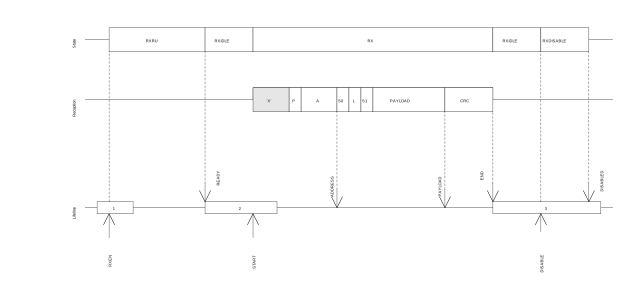
See RXRU in Figure 6 and Figure 10. An RXRU ramp-up sequence is initiated when the RXEN task is triggered. After the radio has successfully ramped up it will generate the READY event indicating that a packet reception can be initiated. A packet reception is initiated by triggering the START task. As illustrated in Figure 6 the START task can, first be triggered after the RADIO has entered into the RXIDLE state.
Figure 10 illustrates a single packet reception where the CPU manually triggers the different tasks needed to control the flow of the RADIO, i.e. no shortcuts are used. If shortcuts are not used, a certain amount of delay, caused by CPU execution, is expected between READY and START, and between END and DISABLE. As illustrated Figure 10 the RADIO will be listening and possibly receiving undefined data, illustrated with an 'X', from START and until a packet with valid preamble (P) is received.
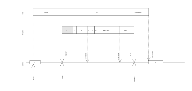
A slightly modified version of the receive sequence from Figure 10 is illustrated in Figure 11 where the the RADIO is configured to use shortcuts between READY and START, and between END and DISABLE, which means that no delay is introduced.
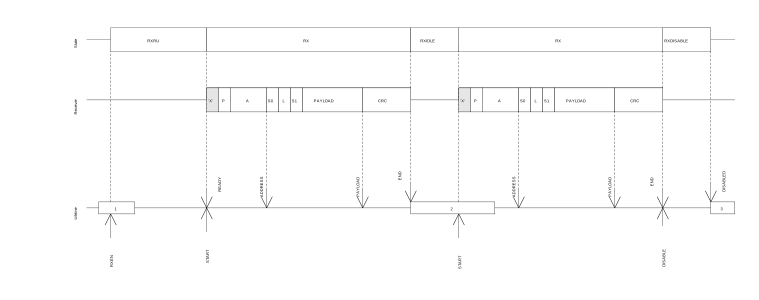
The RADIO is able to receive multiple packets one after the other without having to disable and re-enable the RADIO between packets, this is illustrated Figure 12.
Received Signal Strength Indicator (RSSI)
The radio implements a mechanism for measuring the power in the received radio signal. This feature is called Received Signal Strength Indicator (RSSI).
Sampling of the received signal strength is started by using the RSSISTART task. The sample can be read from the RSSISAMPLE register.
The sample period of the RSSI is defined by RSSIPERIOD, see the device product specification for details. The RSSI sample will hold the average received signal strength during this sample period.
For the RSSI sample to be valid the radio has to be enabled in receive mode (RXEN task) and the reception has to be started (READY event followed by START task).
Interframe spacing
Interframe spacing is the time interval between two consecutive packets.
It is defined as the time, in micro seconds, from the end of the last bit of the previous packet received and to the start of the first bit of the subsequent packet that is transmitted. The RADIO is able to enforce this interval as specified in the TIFS register as long as TIFS is not specified to be shorter than the RADIO’s turn-around time, i.e. the time needed to switch off the receiver, and switch back on the transmitter.
TIFS is only enforced if END_DISABLE and DISABLED_TXEN or END_DISABLE and DISABLED_RXEN shortcuts are enabled. TIFS is only qualified for use in BLE_1MBIT mode, and default ramp-up mode.
Device address match
The device address match feature is tailored for address white listing in a Bluetooth Smart and similar implementations.
This feature enables on-the-fly device address matching while receiving a packet on air. This feature only works in receive mode and as long as RADIO is configured for little endian, see PCNF1.ENDIAN.
The Device Address match unit assumes that the 48 first bits of the payload is the device address and that bit number 6 in S0 is the TxAdd bit. See the Bluetooth Core Specification for more information about device addresses, TxAdd and whitelisting.
The RADIO is able to listen for eight different device addresses at the same time. These addresses are specified in a DAB/DAP register pair, one pair per address, in addition to a TxAdd bit configured in the DACNF register. The DAB register specifies the 32 least significant bits of the device address, while the DAP register specifies the 16 most significant bits of the device address.
Each of the device addresses can be individually included or excluded from the matching mechanism. This is configured in the DACNF register.
Bit counter
The RADIO implements a simple counter that can be configured to generate an event after a specific number of bits have been transmitted or received.
By using shortcuts, this counter can be started from different events generated by the RADIO and hence count relative to these.
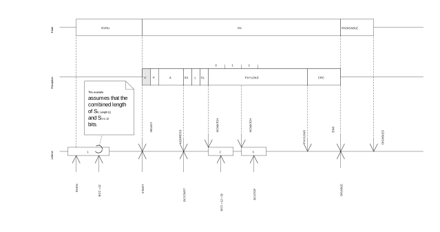
The bit counter is started by triggering the BCSTART task, and stopped by triggering the BCSTOP task. A BCMATCH event will be generated when the bit counter has counted the number of bits specified in the BCC register. The bit counter will continue to count bits until the DISABLED event is generated or until the BCSTOP task is triggered. The CPU can therefore, after a BCMATCH event, reconfigure the BCC value for new BCMATCH events within the same packet.
The bit counter can only be started after the RADIO has received the ADDRESS event.
The bit counter will stop and reset on BCSTOP, STOP, END and DISABLE tasks.
The figure below illustrates how the bit counter can be used to generate a BCMATCH event in the beginning of the packet payload, and again generate a second BCMATCH event after sending 2 bytes (16 bits) of the payload.
Registers
| Base address | Peripheral | Instance | Description | Configuration | |
|---|---|---|---|---|---|
| 0x40001000 | RADIO | RADIO | 2.4 GHz radio | ||
| Register | Offset | Description | |
|---|---|---|---|
| TASKS_TXEN | 0x000 | Enable RADIO in TX mode | |
| TASKS_RXEN | 0x004 | Enable RADIO in RX mode | |
| TASKS_START | 0x008 | Start RADIO | |
| TASKS_STOP | 0x00C | Stop RADIO | |
| TASKS_DISABLE | 0x010 | Disable RADIO | |
| TASKS_RSSISTART | 0x014 | Start the RSSI and take one single sample of the receive signal strength. | |
| TASKS_RSSISTOP | 0x018 | Stop the RSSI measurement | |
| TASKS_BCSTART | 0x01C | Start the bit counter | |
| TASKS_BCSTOP | 0x020 | Stop the bit counter | |
| EVENTS_READY | 0x100 | RADIO has ramped up and is ready to be started | |
| EVENTS_ADDRESS | 0x104 | Address sent or received | |
| EVENTS_PAYLOAD | 0x108 | Packet payload sent or received | |
| EVENTS_END | 0x10C | Packet sent or received | |
| EVENTS_DISABLED | 0x110 | RADIO has been disabled | |
| EVENTS_DEVMATCH | 0x114 | A device address match occurred on the last received packet | |
| EVENTS_DEVMISS | 0x118 | No device address match occurred on the last received packet | |
| EVENTS_RSSIEND | 0x11C | Sampling of receive signal strength complete. | |
| EVENTS_BCMATCH | 0x128 | Bit counter reached bit count value. | |
| EVENTS_CRCOK | 0x130 | Packet received with CRC ok | |
| EVENTS_CRCERROR | 0x134 | Packet received with CRC error | |
| SHORTS | 0x200 | Shortcut register | |
| INTENSET | 0x304 | Enable interrupt | |
| INTENCLR | 0x308 | Disable interrupt | |
| CRCSTATUS | 0x400 | CRC status | |
| RXMATCH | 0x408 | Received address | |
| RXCRC | 0x40C | CRC field of previously received packet | |
| DAI | 0x410 | Device address match index | |
| PACKETPTR | 0x504 | Packet pointer | |
| FREQUENCY | 0x508 | Frequency | |
| TXPOWER | 0x50C | Output power | |
| MODE | 0x510 | Data rate and modulation | |
| PCNF0 | 0x514 | Packet configuration register 0 | |
| PCNF1 | 0x518 | Packet configuration register 1 | |
| BASE0 | 0x51C | Base address 0 | |
| BASE1 | 0x520 | Base address 1 | |
| PREFIX0 | 0x524 | Prefixes bytes for logical addresses 0-3 | |
| PREFIX1 | 0x528 | Prefixes bytes for logical addresses 4-7 | |
| TXADDRESS | 0x52C | Transmit address select | |
| RXADDRESSES | 0x530 | Receive address select | |
| CRCCNF | 0x534 | CRC configuration | |
| CRCPOLY | 0x538 | CRC polynomial | |
| CRCINIT | 0x53C | CRC initial value | |
| 0x540 | Reserved | ||
| TIFS | 0x544 | Inter Frame Spacing in us | |
| RSSISAMPLE | 0x548 | RSSI sample | |
| STATE | 0x550 | Current radio state | |
| DATAWHITEIV | 0x554 | Data whitening initial value | |
| BCC | 0x560 | Bit counter compare | |
| DAB[0] | 0x600 | Device address base segment 0 | |
| DAB[1] | 0x604 | Device address base segment 1 | |
| DAB[2] | 0x608 | Device address base segment 2 | |
| DAB[3] | 0x60C | Device address base segment 3 | |
| DAB[4] | 0x610 | Device address base segment 4 | |
| DAB[5] | 0x614 | Device address base segment 5 | |
| DAB[6] | 0x618 | Device address base segment 6 | |
| DAB[7] | 0x61C | Device address base segment 7 | |
| DAP[0] | 0x620 | Device address prefix 0 | |
| DAP[1] | 0x624 | Device address prefix 1 | |
| DAP[2] | 0x628 | Device address prefix 2 | |
| DAP[3] | 0x62C | Device address prefix 3 | |
| DAP[4] | 0x630 | Device address prefix 4 | |
| DAP[5] | 0x634 | Device address prefix 5 | |
| DAP[6] | 0x638 | Device address prefix 6 | |
| DAP[7] | 0x63C | Device address prefix 7 | |
| DACNF | 0x640 | Device address match configuration | |
| MODECNF0 | 0x650 | Radio mode configuration register 0 | |
| POWER | 0xFFC | Peripheral power control | |
SHORTS
Address offset: 0x200
Shortcut register
| Bit number | 31 | 30 | 29 | 28 | 27 | 26 | 25 | 24 | 23 | 22 | 21 | 20 | 19 | 18 | 17 | 16 | 15 | 14 | 13 | 12 | 11 | 10 | 9 | 8 | 7 | 6 | 5 | 4 | 3 | 2 | 1 | 0 | |||
|---|---|---|---|---|---|---|---|---|---|---|---|---|---|---|---|---|---|---|---|---|---|---|---|---|---|---|---|---|---|---|---|---|---|---|---|
| Id | H | G | F | E | D | C | B | A | |||||||||||||||||||||||||||
| Reset 0x00000000 | 0 | 0 | 0 | 0 | 0 | 0 | 0 | 0 | 0 | 0 | 0 | 0 | 0 | 0 | 0 | 0 | 0 | 0 | 0 | 0 | 0 | 0 | 0 | 0 | 0 | 0 | 0 | 0 | 0 | 0 | 0 | 0 | |||
| Id | RW | Field | Value Id | Value | Description | ||||||||||||||||||||||||||||||
| A | RW | READY_START | Shortcut between READY event and START task See EVENTS_READY and TASKS_START | ||||||||||||||||||||||||||||||||
Disabled | 0 | Disable shortcut | |||||||||||||||||||||||||||||||||
Enabled | 1 | Enable shortcut | |||||||||||||||||||||||||||||||||
| B | RW | END_DISABLE | Shortcut between END event and DISABLE task See EVENTS_END and TASKS_DISABLE | ||||||||||||||||||||||||||||||||
Disabled | 0 | Disable shortcut | |||||||||||||||||||||||||||||||||
Enabled | 1 | Enable shortcut | |||||||||||||||||||||||||||||||||
| C | RW | DISABLED_TXEN | Shortcut between DISABLED event and TXEN task See EVENTS_DISABLED and TASKS_TXEN | ||||||||||||||||||||||||||||||||
Disabled | 0 | Disable shortcut | |||||||||||||||||||||||||||||||||
Enabled | 1 | Enable shortcut | |||||||||||||||||||||||||||||||||
| D | RW | DISABLED_RXEN | Shortcut between DISABLED event and RXEN task See EVENTS_DISABLED and TASKS_RXEN | ||||||||||||||||||||||||||||||||
Disabled | 0 | Disable shortcut | |||||||||||||||||||||||||||||||||
Enabled | 1 | Enable shortcut | |||||||||||||||||||||||||||||||||
| E | RW | ADDRESS_RSSISTART | Shortcut between ADDRESS event and RSSISTART task See EVENTS_ADDRESS and TASKS_RSSISTART | ||||||||||||||||||||||||||||||||
Disabled | 0 | Disable shortcut | |||||||||||||||||||||||||||||||||
Enabled | 1 | Enable shortcut | |||||||||||||||||||||||||||||||||
| F | RW | END_START | Shortcut between END event and START task See EVENTS_END and TASKS_START | ||||||||||||||||||||||||||||||||
Disabled | 0 | Disable shortcut | |||||||||||||||||||||||||||||||||
Enabled | 1 | Enable shortcut | |||||||||||||||||||||||||||||||||
| G | RW | ADDRESS_BCSTART | Shortcut between ADDRESS event and BCSTART task See EVENTS_ADDRESS and TASKS_BCSTART | ||||||||||||||||||||||||||||||||
Disabled | 0 | Disable shortcut | |||||||||||||||||||||||||||||||||
Enabled | 1 | Enable shortcut | |||||||||||||||||||||||||||||||||
| H | RW | DISABLED_RSSISTOP | Shortcut between DISABLED event and RSSISTOP task See EVENTS_DISABLED and TASKS_RSSISTOP | ||||||||||||||||||||||||||||||||
Disabled | 0 | Disable shortcut | |||||||||||||||||||||||||||||||||
Enabled | 1 | Enable shortcut | |||||||||||||||||||||||||||||||||
INTENSET
Address offset: 0x304
Enable interrupt
| Bit number | 31 | 30 | 29 | 28 | 27 | 26 | 25 | 24 | 23 | 22 | 21 | 20 | 19 | 18 | 17 | 16 | 15 | 14 | 13 | 12 | 11 | 10 | 9 | 8 | 7 | 6 | 5 | 4 | 3 | 2 | 1 | 0 | |||
|---|---|---|---|---|---|---|---|---|---|---|---|---|---|---|---|---|---|---|---|---|---|---|---|---|---|---|---|---|---|---|---|---|---|---|---|
| Id | L | K | I | H | G | F | E | D | C | B | A | ||||||||||||||||||||||||
| Reset 0x00000000 | 0 | 0 | 0 | 0 | 0 | 0 | 0 | 0 | 0 | 0 | 0 | 0 | 0 | 0 | 0 | 0 | 0 | 0 | 0 | 0 | 0 | 0 | 0 | 0 | 0 | 0 | 0 | 0 | 0 | 0 | 0 | 0 | |||
| Id | RW | Field | Value Id | Value | Description | ||||||||||||||||||||||||||||||
| A | RW | READY | Write '1' to Enable interrupt for READY event See EVENTS_READY | ||||||||||||||||||||||||||||||||
Set | 1 | Enable | |||||||||||||||||||||||||||||||||
Disabled | 0 | Read: Disabled | |||||||||||||||||||||||||||||||||
Enabled | 1 | Read: Enabled | |||||||||||||||||||||||||||||||||
| B | RW | ADDRESS | Write '1' to Enable interrupt for ADDRESS event See EVENTS_ADDRESS | ||||||||||||||||||||||||||||||||
Set | 1 | Enable | |||||||||||||||||||||||||||||||||
Disabled | 0 | Read: Disabled | |||||||||||||||||||||||||||||||||
Enabled | 1 | Read: Enabled | |||||||||||||||||||||||||||||||||
| C | RW | PAYLOAD | Write '1' to Enable interrupt for PAYLOAD event See EVENTS_PAYLOAD | ||||||||||||||||||||||||||||||||
Set | 1 | Enable | |||||||||||||||||||||||||||||||||
Disabled | 0 | Read: Disabled | |||||||||||||||||||||||||||||||||
Enabled | 1 | Read: Enabled | |||||||||||||||||||||||||||||||||
| D | RW | END | Write '1' to Enable interrupt for END event See EVENTS_END | ||||||||||||||||||||||||||||||||
Set | 1 | Enable | |||||||||||||||||||||||||||||||||
Disabled | 0 | Read: Disabled | |||||||||||||||||||||||||||||||||
Enabled | 1 | Read: Enabled | |||||||||||||||||||||||||||||||||
| E | RW | DISABLED | Write '1' to Enable interrupt for DISABLED event See EVENTS_DISABLED | ||||||||||||||||||||||||||||||||
Set | 1 | Enable | |||||||||||||||||||||||||||||||||
Disabled | 0 | Read: Disabled | |||||||||||||||||||||||||||||||||
Enabled | 1 | Read: Enabled | |||||||||||||||||||||||||||||||||
| F | RW | DEVMATCH | Write '1' to Enable interrupt for DEVMATCH event See EVENTS_DEVMATCH | ||||||||||||||||||||||||||||||||
Set | 1 | Enable | |||||||||||||||||||||||||||||||||
Disabled | 0 | Read: Disabled | |||||||||||||||||||||||||||||||||
Enabled | 1 | Read: Enabled | |||||||||||||||||||||||||||||||||
| G | RW | DEVMISS | Write '1' to Enable interrupt for DEVMISS event See EVENTS_DEVMISS | ||||||||||||||||||||||||||||||||
Set | 1 | Enable | |||||||||||||||||||||||||||||||||
Disabled | 0 | Read: Disabled | |||||||||||||||||||||||||||||||||
Enabled | 1 | Read: Enabled | |||||||||||||||||||||||||||||||||
| H | RW | RSSIEND | Write '1' to Enable interrupt for RSSIEND event See EVENTS_RSSIEND | ||||||||||||||||||||||||||||||||
Set | 1 | Enable | |||||||||||||||||||||||||||||||||
Disabled | 0 | Read: Disabled | |||||||||||||||||||||||||||||||||
Enabled | 1 | Read: Enabled | |||||||||||||||||||||||||||||||||
| I | RW | BCMATCH | Write '1' to Enable interrupt for BCMATCH event See EVENTS_BCMATCH | ||||||||||||||||||||||||||||||||
Set | 1 | Enable | |||||||||||||||||||||||||||||||||
Disabled | 0 | Read: Disabled | |||||||||||||||||||||||||||||||||
Enabled | 1 | Read: Enabled | |||||||||||||||||||||||||||||||||
| K | RW | CRCOK | Write '1' to Enable interrupt for CRCOK event See EVENTS_CRCOK | ||||||||||||||||||||||||||||||||
Set | 1 | Enable | |||||||||||||||||||||||||||||||||
Disabled | 0 | Read: Disabled | |||||||||||||||||||||||||||||||||
Enabled | 1 | Read: Enabled | |||||||||||||||||||||||||||||||||
| L | RW | CRCERROR | Write '1' to Enable interrupt for CRCERROR event See EVENTS_CRCERROR | ||||||||||||||||||||||||||||||||
Set | 1 | Enable | |||||||||||||||||||||||||||||||||
Disabled | 0 | Read: Disabled | |||||||||||||||||||||||||||||||||
Enabled | 1 | Read: Enabled | |||||||||||||||||||||||||||||||||
INTENCLR
Address offset: 0x308
Disable interrupt
| Bit number | 31 | 30 | 29 | 28 | 27 | 26 | 25 | 24 | 23 | 22 | 21 | 20 | 19 | 18 | 17 | 16 | 15 | 14 | 13 | 12 | 11 | 10 | 9 | 8 | 7 | 6 | 5 | 4 | 3 | 2 | 1 | 0 | |||
|---|---|---|---|---|---|---|---|---|---|---|---|---|---|---|---|---|---|---|---|---|---|---|---|---|---|---|---|---|---|---|---|---|---|---|---|
| Id | L | K | I | H | G | F | E | D | C | B | A | ||||||||||||||||||||||||
| Reset 0x00000000 | 0 | 0 | 0 | 0 | 0 | 0 | 0 | 0 | 0 | 0 | 0 | 0 | 0 | 0 | 0 | 0 | 0 | 0 | 0 | 0 | 0 | 0 | 0 | 0 | 0 | 0 | 0 | 0 | 0 | 0 | 0 | 0 | |||
| Id | RW | Field | Value Id | Value | Description | ||||||||||||||||||||||||||||||
| A | RW | READY | Write '1' to Disable interrupt for READY event See EVENTS_READY | ||||||||||||||||||||||||||||||||
Clear | 1 | Disable | |||||||||||||||||||||||||||||||||
Disabled | 0 | Read: Disabled | |||||||||||||||||||||||||||||||||
Enabled | 1 | Read: Enabled | |||||||||||||||||||||||||||||||||
| B | RW | ADDRESS | Write '1' to Disable interrupt for ADDRESS event See EVENTS_ADDRESS | ||||||||||||||||||||||||||||||||
Clear | 1 | Disable | |||||||||||||||||||||||||||||||||
Disabled | 0 | Read: Disabled | |||||||||||||||||||||||||||||||||
Enabled | 1 | Read: Enabled | |||||||||||||||||||||||||||||||||
| C | RW | PAYLOAD | Write '1' to Disable interrupt for PAYLOAD event See EVENTS_PAYLOAD | ||||||||||||||||||||||||||||||||
Clear | 1 | Disable | |||||||||||||||||||||||||||||||||
Disabled | 0 | Read: Disabled | |||||||||||||||||||||||||||||||||
Enabled | 1 | Read: Enabled | |||||||||||||||||||||||||||||||||
| D | RW | END | Write '1' to Disable interrupt for END event See EVENTS_END | ||||||||||||||||||||||||||||||||
Clear | 1 | Disable | |||||||||||||||||||||||||||||||||
Disabled | 0 | Read: Disabled | |||||||||||||||||||||||||||||||||
Enabled | 1 | Read: Enabled | |||||||||||||||||||||||||||||||||
| E | RW | DISABLED | Write '1' to Disable interrupt for DISABLED event See EVENTS_DISABLED | ||||||||||||||||||||||||||||||||
Clear | 1 | Disable | |||||||||||||||||||||||||||||||||
Disabled | 0 | Read: Disabled | |||||||||||||||||||||||||||||||||
Enabled | 1 | Read: Enabled | |||||||||||||||||||||||||||||||||
| F | RW | DEVMATCH | Write '1' to Disable interrupt for DEVMATCH event See EVENTS_DEVMATCH | ||||||||||||||||||||||||||||||||
Clear | 1 | Disable | |||||||||||||||||||||||||||||||||
Disabled | 0 | Read: Disabled | |||||||||||||||||||||||||||||||||
Enabled | 1 | Read: Enabled | |||||||||||||||||||||||||||||||||
| G | RW | DEVMISS | Write '1' to Disable interrupt for DEVMISS event See EVENTS_DEVMISS | ||||||||||||||||||||||||||||||||
Clear | 1 | Disable | |||||||||||||||||||||||||||||||||
Disabled | 0 | Read: Disabled | |||||||||||||||||||||||||||||||||
Enabled | 1 | Read: Enabled | |||||||||||||||||||||||||||||||||
| H | RW | RSSIEND | Write '1' to Disable interrupt for RSSIEND event See EVENTS_RSSIEND | ||||||||||||||||||||||||||||||||
Clear | 1 | Disable | |||||||||||||||||||||||||||||||||
Disabled | 0 | Read: Disabled | |||||||||||||||||||||||||||||||||
Enabled | 1 | Read: Enabled | |||||||||||||||||||||||||||||||||
| I | RW | BCMATCH | Write '1' to Disable interrupt for BCMATCH event See EVENTS_BCMATCH | ||||||||||||||||||||||||||||||||
Clear | 1 | Disable | |||||||||||||||||||||||||||||||||
Disabled | 0 | Read: Disabled | |||||||||||||||||||||||||||||||||
Enabled | 1 | Read: Enabled | |||||||||||||||||||||||||||||||||
| K | RW | CRCOK | Write '1' to Disable interrupt for CRCOK event See EVENTS_CRCOK | ||||||||||||||||||||||||||||||||
Clear | 1 | Disable | |||||||||||||||||||||||||||||||||
Disabled | 0 | Read: Disabled | |||||||||||||||||||||||||||||||||
Enabled | 1 | Read: Enabled | |||||||||||||||||||||||||||||||||
| L | RW | CRCERROR | Write '1' to Disable interrupt for CRCERROR event See EVENTS_CRCERROR | ||||||||||||||||||||||||||||||||
Clear | 1 | Disable | |||||||||||||||||||||||||||||||||
Disabled | 0 | Read: Disabled | |||||||||||||||||||||||||||||||||
Enabled | 1 | Read: Enabled | |||||||||||||||||||||||||||||||||
CRCSTATUS
Address offset: 0x400
CRC status
| Bit number | 31 | 30 | 29 | 28 | 27 | 26 | 25 | 24 | 23 | 22 | 21 | 20 | 19 | 18 | 17 | 16 | 15 | 14 | 13 | 12 | 11 | 10 | 9 | 8 | 7 | 6 | 5 | 4 | 3 | 2 | 1 | 0 | |||
|---|---|---|---|---|---|---|---|---|---|---|---|---|---|---|---|---|---|---|---|---|---|---|---|---|---|---|---|---|---|---|---|---|---|---|---|
| Id | A | ||||||||||||||||||||||||||||||||||
| Reset 0x00000000 | 0 | 0 | 0 | 0 | 0 | 0 | 0 | 0 | 0 | 0 | 0 | 0 | 0 | 0 | 0 | 0 | 0 | 0 | 0 | 0 | 0 | 0 | 0 | 0 | 0 | 0 | 0 | 0 | 0 | 0 | 0 | 0 | |||
| Id | RW | Field | Value Id | Value | Description | ||||||||||||||||||||||||||||||
| A | R | CRCSTATUS | CRC status of packet received | ||||||||||||||||||||||||||||||||
CRCError | 0 | Packet received with CRC error | |||||||||||||||||||||||||||||||||
CRCOk | 1 | Packet received with CRC ok | |||||||||||||||||||||||||||||||||
RXMATCH
Address offset: 0x408
Received address
| Bit number | 31 | 30 | 29 | 28 | 27 | 26 | 25 | 24 | 23 | 22 | 21 | 20 | 19 | 18 | 17 | 16 | 15 | 14 | 13 | 12 | 11 | 10 | 9 | 8 | 7 | 6 | 5 | 4 | 3 | 2 | 1 | 0 | |||
|---|---|---|---|---|---|---|---|---|---|---|---|---|---|---|---|---|---|---|---|---|---|---|---|---|---|---|---|---|---|---|---|---|---|---|---|
| Id | A | A | A | ||||||||||||||||||||||||||||||||
| Reset 0x00000000 | 0 | 0 | 0 | 0 | 0 | 0 | 0 | 0 | 0 | 0 | 0 | 0 | 0 | 0 | 0 | 0 | 0 | 0 | 0 | 0 | 0 | 0 | 0 | 0 | 0 | 0 | 0 | 0 | 0 | 0 | 0 | 0 | |||
| Id | RW | Field | Value Id | Value | Description | ||||||||||||||||||||||||||||||
| A | R | RXMATCH | Received address Logical address of which previous packet was received | ||||||||||||||||||||||||||||||||
RXCRC
Address offset: 0x40C
CRC field of previously received packet
| Bit number | 31 | 30 | 29 | 28 | 27 | 26 | 25 | 24 | 23 | 22 | 21 | 20 | 19 | 18 | 17 | 16 | 15 | 14 | 13 | 12 | 11 | 10 | 9 | 8 | 7 | 6 | 5 | 4 | 3 | 2 | 1 | 0 | |||
|---|---|---|---|---|---|---|---|---|---|---|---|---|---|---|---|---|---|---|---|---|---|---|---|---|---|---|---|---|---|---|---|---|---|---|---|
| Id | A | A | A | A | A | A | A | A | A | A | A | A | A | A | A | A | A | A | A | A | A | A | A | A | |||||||||||
| Reset 0x00000000 | 0 | 0 | 0 | 0 | 0 | 0 | 0 | 0 | 0 | 0 | 0 | 0 | 0 | 0 | 0 | 0 | 0 | 0 | 0 | 0 | 0 | 0 | 0 | 0 | 0 | 0 | 0 | 0 | 0 | 0 | 0 | 0 | |||
| Id | RW | Field | Value Id | Value | Description | ||||||||||||||||||||||||||||||
| A | R | RXCRC | CRC field of previously received packet CRC field of previously received packet | ||||||||||||||||||||||||||||||||
DAI
Address offset: 0x410
Device address match index
| Bit number | 31 | 30 | 29 | 28 | 27 | 26 | 25 | 24 | 23 | 22 | 21 | 20 | 19 | 18 | 17 | 16 | 15 | 14 | 13 | 12 | 11 | 10 | 9 | 8 | 7 | 6 | 5 | 4 | 3 | 2 | 1 | 0 | |||
|---|---|---|---|---|---|---|---|---|---|---|---|---|---|---|---|---|---|---|---|---|---|---|---|---|---|---|---|---|---|---|---|---|---|---|---|
| Id | A | A | A | ||||||||||||||||||||||||||||||||
| Reset 0x00000000 | 0 | 0 | 0 | 0 | 0 | 0 | 0 | 0 | 0 | 0 | 0 | 0 | 0 | 0 | 0 | 0 | 0 | 0 | 0 | 0 | 0 | 0 | 0 | 0 | 0 | 0 | 0 | 0 | 0 | 0 | 0 | 0 | |||
| Id | RW | Field | Value Id | Value | Description | ||||||||||||||||||||||||||||||
| A | R | DAI | Device address match index Index (n) of device address, see DAB[n] and DAP[n], that got an address match. | ||||||||||||||||||||||||||||||||
PACKETPTR
Address offset: 0x504
Packet pointer
| Bit number | 31 | 30 | 29 | 28 | 27 | 26 | 25 | 24 | 23 | 22 | 21 | 20 | 19 | 18 | 17 | 16 | 15 | 14 | 13 | 12 | 11 | 10 | 9 | 8 | 7 | 6 | 5 | 4 | 3 | 2 | 1 | 0 | |||
|---|---|---|---|---|---|---|---|---|---|---|---|---|---|---|---|---|---|---|---|---|---|---|---|---|---|---|---|---|---|---|---|---|---|---|---|
| Id | A | A | A | A | A | A | A | A | A | A | A | A | A | A | A | A | A | A | A | A | A | A | A | A | A | A | A | A | A | A | A | A | |||
| Reset 0x00000000 | 0 | 0 | 0 | 0 | 0 | 0 | 0 | 0 | 0 | 0 | 0 | 0 | 0 | 0 | 0 | 0 | 0 | 0 | 0 | 0 | 0 | 0 | 0 | 0 | 0 | 0 | 0 | 0 | 0 | 0 | 0 | 0 | |||
| Id | RW | Field | Value Id | Value | Description | ||||||||||||||||||||||||||||||
| A | RW | PACKETPTR | Packet pointer Packet address to be used for the next transmission or reception. When transmitting, the packet pointed to by this address will be transmitted and when receiving, the received packet will be written to this address. This address is a byte aligned ram address. | ||||||||||||||||||||||||||||||||
FREQUENCY
Address offset: 0x508
Frequency
| Bit number | 31 | 30 | 29 | 28 | 27 | 26 | 25 | 24 | 23 | 22 | 21 | 20 | 19 | 18 | 17 | 16 | 15 | 14 | 13 | 12 | 11 | 10 | 9 | 8 | 7 | 6 | 5 | 4 | 3 | 2 | 1 | 0 | |||
|---|---|---|---|---|---|---|---|---|---|---|---|---|---|---|---|---|---|---|---|---|---|---|---|---|---|---|---|---|---|---|---|---|---|---|---|
| Id | B | A | A | A | A | A | A | A | |||||||||||||||||||||||||||
| Reset 0x00000002 | 0 | 0 | 0 | 0 | 0 | 0 | 0 | 0 | 0 | 0 | 0 | 0 | 0 | 0 | 0 | 0 | 0 | 0 | 0 | 0 | 0 | 0 | 0 | 0 | 0 | 0 | 0 | 0 | 0 | 0 | 1 | 0 | |||
| Id | RW | Field | Value Id | Value | Description | ||||||||||||||||||||||||||||||
| A | RW | FREQUENCY | [0..100] | Radio channel frequency Frequency = 2400 + FREQUENCY (MHz). | |||||||||||||||||||||||||||||||
| B | RW | MAP | Channel map selection. | ||||||||||||||||||||||||||||||||
Default | 0 | Channel map between 2400 MHZ .. 2500 MHz Frequency = 2400 + FREQUENCY (MHz) | |||||||||||||||||||||||||||||||||
Low | 1 | Channel map between 2360 MHZ .. 2460 MHz Frequency = 2360 + FREQUENCY (MHz) | |||||||||||||||||||||||||||||||||
TXPOWER
Address offset: 0x50C
Output power
| Bit number | 31 | 30 | 29 | 28 | 27 | 26 | 25 | 24 | 23 | 22 | 21 | 20 | 19 | 18 | 17 | 16 | 15 | 14 | 13 | 12 | 11 | 10 | 9 | 8 | 7 | 6 | 5 | 4 | 3 | 2 | 1 | 0 | |||
|---|---|---|---|---|---|---|---|---|---|---|---|---|---|---|---|---|---|---|---|---|---|---|---|---|---|---|---|---|---|---|---|---|---|---|---|
| Id | A | A | A | A | A | A | A | A | |||||||||||||||||||||||||||
| Reset 0x00000000 | 0 | 0 | 0 | 0 | 0 | 0 | 0 | 0 | 0 | 0 | 0 | 0 | 0 | 0 | 0 | 0 | 0 | 0 | 0 | 0 | 0 | 0 | 0 | 0 | 0 | 0 | 0 | 0 | 0 | 0 | 0 | 0 | |||
| Id | RW | Field | Value Id | Value | Description | ||||||||||||||||||||||||||||||
| A | RW | TXPOWER | RADIO output power. Output power in number of dBm, i.e. if the value -20 is specified the output power will be set to -20dBm. | ||||||||||||||||||||||||||||||||
Pos4dBm | 0x04 | +4 dBm | |||||||||||||||||||||||||||||||||
Pos3dBm | 0x03 | +3 dBm | |||||||||||||||||||||||||||||||||
0dBm | 0x00 | 0 dBm | |||||||||||||||||||||||||||||||||
Neg4dBm | 0xFC | -4 dBm | |||||||||||||||||||||||||||||||||
Neg8dBm | 0xF8 | -8 dBm | |||||||||||||||||||||||||||||||||
Neg12dBm | 0xF4 | -12 dBm | |||||||||||||||||||||||||||||||||
Neg16dBm | 0xF0 | -16 dBm | |||||||||||||||||||||||||||||||||
Neg20dBm | 0xEC | -20 dBm | |||||||||||||||||||||||||||||||||
Neg30dBm | 0xD8 | -40 dBm | Deprecated | ||||||||||||||||||||||||||||||||
Neg40dBm | 0xD8 | -40 dBm | |||||||||||||||||||||||||||||||||
MODE
Address offset: 0x510
Data rate and modulation
| Bit number | 31 | 30 | 29 | 28 | 27 | 26 | 25 | 24 | 23 | 22 | 21 | 20 | 19 | 18 | 17 | 16 | 15 | 14 | 13 | 12 | 11 | 10 | 9 | 8 | 7 | 6 | 5 | 4 | 3 | 2 | 1 | 0 | |||
|---|---|---|---|---|---|---|---|---|---|---|---|---|---|---|---|---|---|---|---|---|---|---|---|---|---|---|---|---|---|---|---|---|---|---|---|
| Id | A | A | A | A | |||||||||||||||||||||||||||||||
| Reset 0x00000000 | 0 | 0 | 0 | 0 | 0 | 0 | 0 | 0 | 0 | 0 | 0 | 0 | 0 | 0 | 0 | 0 | 0 | 0 | 0 | 0 | 0 | 0 | 0 | 0 | 0 | 0 | 0 | 0 | 0 | 0 | 0 | 0 | |||
| Id | RW | Field | Value Id | Value | Description | ||||||||||||||||||||||||||||||
| A | RW | MODE | Radio data rate and modulation setting. The radio supports Frequency-shift Keying (FSK) modulation. | ||||||||||||||||||||||||||||||||
Nrf_1Mbit | 0 | 1 Mbit/s Nordic proprietary radio mode | |||||||||||||||||||||||||||||||||
Nrf_2Mbit | 1 | 2 Mbit/s Nordic proprietary radio mode | |||||||||||||||||||||||||||||||||
Nrf_250Kbit | 2 | 250 kbit/s Nordic proprietary radio mode | Deprecated | ||||||||||||||||||||||||||||||||
Ble_1Mbit | 3 | 1 Mbit/s Bluetooth Low Energy | |||||||||||||||||||||||||||||||||
Ble_2Mbit | 4 | 2 Mbit/s Bluetooth Low Energy | |||||||||||||||||||||||||||||||||
PCNF0
Address offset: 0x514
Packet configuration register 0
| Bit number | 31 | 30 | 29 | 28 | 27 | 26 | 25 | 24 | 23 | 22 | 21 | 20 | 19 | 18 | 17 | 16 | 15 | 14 | 13 | 12 | 11 | 10 | 9 | 8 | 7 | 6 | 5 | 4 | 3 | 2 | 1 | 0 | |||
|---|---|---|---|---|---|---|---|---|---|---|---|---|---|---|---|---|---|---|---|---|---|---|---|---|---|---|---|---|---|---|---|---|---|---|---|
| Id | G | F | E | E | E | E | C | A | A | A | A | ||||||||||||||||||||||||
| Reset 0x00000000 | 0 | 0 | 0 | 0 | 0 | 0 | 0 | 0 | 0 | 0 | 0 | 0 | 0 | 0 | 0 | 0 | 0 | 0 | 0 | 0 | 0 | 0 | 0 | 0 | 0 | 0 | 0 | 0 | 0 | 0 | 0 | 0 | |||
| Id | RW | Field | Value Id | Value | Description | ||||||||||||||||||||||||||||||
| A | RW | LFLEN | Length on air of LENGTH field in number of bits. | ||||||||||||||||||||||||||||||||
| C | RW | S0LEN | Length on air of S0 field in number of bytes. | ||||||||||||||||||||||||||||||||
| E | RW | S1LEN | Length on air of S1 field in number of bits. | ||||||||||||||||||||||||||||||||
| F | RW | S1INCL | Include or exclude S1 field in RAM | ||||||||||||||||||||||||||||||||
Automatic | 0 | Include S1 field in RAM only if S1LEN > 0 | |||||||||||||||||||||||||||||||||
Include | 1 | Always include S1 field in RAM independent of S1LEN | |||||||||||||||||||||||||||||||||
| G | RW | PLEN | Length of preamble on air. Decision point: TASKS_START task | ||||||||||||||||||||||||||||||||
8bit | 0 | 8-bit preamble | |||||||||||||||||||||||||||||||||
16bit | 1 | 16-bit preamble | |||||||||||||||||||||||||||||||||
PCNF1
Address offset: 0x518
Packet configuration register 1
| Bit number | 31 | 30 | 29 | 28 | 27 | 26 | 25 | 24 | 23 | 22 | 21 | 20 | 19 | 18 | 17 | 16 | 15 | 14 | 13 | 12 | 11 | 10 | 9 | 8 | 7 | 6 | 5 | 4 | 3 | 2 | 1 | 0 | |||
|---|---|---|---|---|---|---|---|---|---|---|---|---|---|---|---|---|---|---|---|---|---|---|---|---|---|---|---|---|---|---|---|---|---|---|---|
| Id | E | D | C | C | C | B | B | B | B | B | B | B | B | A | A | A | A | A | A | A | A | ||||||||||||||
| Reset 0x00000000 | 0 | 0 | 0 | 0 | 0 | 0 | 0 | 0 | 0 | 0 | 0 | 0 | 0 | 0 | 0 | 0 | 0 | 0 | 0 | 0 | 0 | 0 | 0 | 0 | 0 | 0 | 0 | 0 | 0 | 0 | 0 | 0 | |||
| Id | RW | Field | Value Id | Value | Description | ||||||||||||||||||||||||||||||
| A | RW | MAXLEN | [0..255] | Maximum length of packet payload. If the packet payload is larger than MAXLEN, the radio will truncate the payload to MAXLEN. | |||||||||||||||||||||||||||||||
| B | RW | STATLEN | [0..255] | Static length in number of bytes The static length parameter is added to the total length of the payload when sending and receiving packets, e.g. if the static length is set to N the radio will receive or send N bytes more than what is defined in the LENGTH field of the packet. | |||||||||||||||||||||||||||||||
| C | RW | BALEN | [2..4] | Base address length in number of bytes The address field is composed of the base address and the one byte long address prefix, e.g. set BALEN=2 to get a total address of 3 bytes. | |||||||||||||||||||||||||||||||
| D | RW | ENDIAN | On air endianness of packet, this applies to the S0, LENGTH, S1 and the PAYLOAD fields. | ||||||||||||||||||||||||||||||||
Little | 0 | Least Significant bit on air first | |||||||||||||||||||||||||||||||||
Big | 1 | Most significant bit on air first | |||||||||||||||||||||||||||||||||
| E | RW | WHITEEN | Enable or disable packet whitening | ||||||||||||||||||||||||||||||||
Disabled | 0 | Disable | |||||||||||||||||||||||||||||||||
Enabled | 1 | Enable | |||||||||||||||||||||||||||||||||
BASE0
Address offset: 0x51C
Base address 0
| Bit number | 31 | 30 | 29 | 28 | 27 | 26 | 25 | 24 | 23 | 22 | 21 | 20 | 19 | 18 | 17 | 16 | 15 | 14 | 13 | 12 | 11 | 10 | 9 | 8 | 7 | 6 | 5 | 4 | 3 | 2 | 1 | 0 | |||
|---|---|---|---|---|---|---|---|---|---|---|---|---|---|---|---|---|---|---|---|---|---|---|---|---|---|---|---|---|---|---|---|---|---|---|---|
| Id | A | A | A | A | A | A | A | A | A | A | A | A | A | A | A | A | A | A | A | A | A | A | A | A | A | A | A | A | A | A | A | A | |||
| Reset 0x00000000 | 0 | 0 | 0 | 0 | 0 | 0 | 0 | 0 | 0 | 0 | 0 | 0 | 0 | 0 | 0 | 0 | 0 | 0 | 0 | 0 | 0 | 0 | 0 | 0 | 0 | 0 | 0 | 0 | 0 | 0 | 0 | 0 | |||
| Id | RW | Field | Value Id | Value | Description | ||||||||||||||||||||||||||||||
| A | RW | BASE0 | Base address 0 Radio base address 0. | ||||||||||||||||||||||||||||||||
BASE1
Address offset: 0x520
Base address 1
| Bit number | 31 | 30 | 29 | 28 | 27 | 26 | 25 | 24 | 23 | 22 | 21 | 20 | 19 | 18 | 17 | 16 | 15 | 14 | 13 | 12 | 11 | 10 | 9 | 8 | 7 | 6 | 5 | 4 | 3 | 2 | 1 | 0 | |||
|---|---|---|---|---|---|---|---|---|---|---|---|---|---|---|---|---|---|---|---|---|---|---|---|---|---|---|---|---|---|---|---|---|---|---|---|
| Id | A | A | A | A | A | A | A | A | A | A | A | A | A | A | A | A | A | A | A | A | A | A | A | A | A | A | A | A | A | A | A | A | |||
| Reset 0x00000000 | 0 | 0 | 0 | 0 | 0 | 0 | 0 | 0 | 0 | 0 | 0 | 0 | 0 | 0 | 0 | 0 | 0 | 0 | 0 | 0 | 0 | 0 | 0 | 0 | 0 | 0 | 0 | 0 | 0 | 0 | 0 | 0 | |||
| Id | RW | Field | Value Id | Value | Description | ||||||||||||||||||||||||||||||
| A | RW | BASE1 | Base address 1 Radio base address 1. | ||||||||||||||||||||||||||||||||
PREFIX0
Address offset: 0x524
Prefixes bytes for logical addresses 0-3
| Bit number | 31 | 30 | 29 | 28 | 27 | 26 | 25 | 24 | 23 | 22 | 21 | 20 | 19 | 18 | 17 | 16 | 15 | 14 | 13 | 12 | 11 | 10 | 9 | 8 | 7 | 6 | 5 | 4 | 3 | 2 | 1 | 0 | |||
|---|---|---|---|---|---|---|---|---|---|---|---|---|---|---|---|---|---|---|---|---|---|---|---|---|---|---|---|---|---|---|---|---|---|---|---|
| Id | D | D | D | D | D | D | D | D | C | C | C | C | C | C | C | C | B | B | B | B | B | B | B | B | A | A | A | A | A | A | A | A | |||
| Reset 0x00000000 | 0 | 0 | 0 | 0 | 0 | 0 | 0 | 0 | 0 | 0 | 0 | 0 | 0 | 0 | 0 | 0 | 0 | 0 | 0 | 0 | 0 | 0 | 0 | 0 | 0 | 0 | 0 | 0 | 0 | 0 | 0 | 0 | |||
| Id | RW | Field | Value Id | Value | Description | ||||||||||||||||||||||||||||||
| A | RW | AP0 | Address prefix 0. | ||||||||||||||||||||||||||||||||
| B | RW | AP1 | Address prefix 1. | ||||||||||||||||||||||||||||||||
| C | RW | AP2 | Address prefix 2. | ||||||||||||||||||||||||||||||||
| D | RW | AP3 | Address prefix 3. | ||||||||||||||||||||||||||||||||
PREFIX1
Address offset: 0x528
Prefixes bytes for logical addresses 4-7
| Bit number | 31 | 30 | 29 | 28 | 27 | 26 | 25 | 24 | 23 | 22 | 21 | 20 | 19 | 18 | 17 | 16 | 15 | 14 | 13 | 12 | 11 | 10 | 9 | 8 | 7 | 6 | 5 | 4 | 3 | 2 | 1 | 0 | |||
|---|---|---|---|---|---|---|---|---|---|---|---|---|---|---|---|---|---|---|---|---|---|---|---|---|---|---|---|---|---|---|---|---|---|---|---|
| Id | D | D | D | D | D | D | D | D | C | C | C | C | C | C | C | C | B | B | B | B | B | B | B | B | A | A | A | A | A | A | A | A | |||
| Reset 0x00000000 | 0 | 0 | 0 | 0 | 0 | 0 | 0 | 0 | 0 | 0 | 0 | 0 | 0 | 0 | 0 | 0 | 0 | 0 | 0 | 0 | 0 | 0 | 0 | 0 | 0 | 0 | 0 | 0 | 0 | 0 | 0 | 0 | |||
| Id | RW | Field | Value Id | Value | Description | ||||||||||||||||||||||||||||||
| A | RW | AP4 | Address prefix 4. | ||||||||||||||||||||||||||||||||
| B | RW | AP5 | Address prefix 5. | ||||||||||||||||||||||||||||||||
| C | RW | AP6 | Address prefix 6. | ||||||||||||||||||||||||||||||||
| D | RW | AP7 | Address prefix 7. | ||||||||||||||||||||||||||||||||
TXADDRESS
Address offset: 0x52C
Transmit address select
| Bit number | 31 | 30 | 29 | 28 | 27 | 26 | 25 | 24 | 23 | 22 | 21 | 20 | 19 | 18 | 17 | 16 | 15 | 14 | 13 | 12 | 11 | 10 | 9 | 8 | 7 | 6 | 5 | 4 | 3 | 2 | 1 | 0 | |||
|---|---|---|---|---|---|---|---|---|---|---|---|---|---|---|---|---|---|---|---|---|---|---|---|---|---|---|---|---|---|---|---|---|---|---|---|
| Id | A | A | A | ||||||||||||||||||||||||||||||||
| Reset 0x00000000 | 0 | 0 | 0 | 0 | 0 | 0 | 0 | 0 | 0 | 0 | 0 | 0 | 0 | 0 | 0 | 0 | 0 | 0 | 0 | 0 | 0 | 0 | 0 | 0 | 0 | 0 | 0 | 0 | 0 | 0 | 0 | 0 | |||
| Id | RW | Field | Value Id | Value | Description | ||||||||||||||||||||||||||||||
| A | RW | TXADDRESS | Transmit address select Logical address to be used when transmitting a packet. | ||||||||||||||||||||||||||||||||
RXADDRESSES
Address offset: 0x530
Receive address select
| Bit number | 31 | 30 | 29 | 28 | 27 | 26 | 25 | 24 | 23 | 22 | 21 | 20 | 19 | 18 | 17 | 16 | 15 | 14 | 13 | 12 | 11 | 10 | 9 | 8 | 7 | 6 | 5 | 4 | 3 | 2 | 1 | 0 | |||
|---|---|---|---|---|---|---|---|---|---|---|---|---|---|---|---|---|---|---|---|---|---|---|---|---|---|---|---|---|---|---|---|---|---|---|---|
| Id | H | G | F | E | D | C | B | A | |||||||||||||||||||||||||||
| Reset 0x00000000 | 0 | 0 | 0 | 0 | 0 | 0 | 0 | 0 | 0 | 0 | 0 | 0 | 0 | 0 | 0 | 0 | 0 | 0 | 0 | 0 | 0 | 0 | 0 | 0 | 0 | 0 | 0 | 0 | 0 | 0 | 0 | 0 | |||
| Id | RW | Field | Value Id | Value | Description | ||||||||||||||||||||||||||||||
| A | RW | ADDR0 | Enable or disable reception on logical address 0. | ||||||||||||||||||||||||||||||||
Disabled | 0 | Disable | |||||||||||||||||||||||||||||||||
Enabled | 1 | Enable | |||||||||||||||||||||||||||||||||
| B | RW | ADDR1 | Enable or disable reception on logical address 1. | ||||||||||||||||||||||||||||||||
Disabled | 0 | Disable | |||||||||||||||||||||||||||||||||
Enabled | 1 | Enable | |||||||||||||||||||||||||||||||||
| C | RW | ADDR2 | Enable or disable reception on logical address 2. | ||||||||||||||||||||||||||||||||
Disabled | 0 | Disable | |||||||||||||||||||||||||||||||||
Enabled | 1 | Enable | |||||||||||||||||||||||||||||||||
| D | RW | ADDR3 | Enable or disable reception on logical address 3. | ||||||||||||||||||||||||||||||||
Disabled | 0 | Disable | |||||||||||||||||||||||||||||||||
Enabled | 1 | Enable | |||||||||||||||||||||||||||||||||
| E | RW | ADDR4 | Enable or disable reception on logical address 4. | ||||||||||||||||||||||||||||||||
Disabled | 0 | Disable | |||||||||||||||||||||||||||||||||
Enabled | 1 | Enable | |||||||||||||||||||||||||||||||||
| F | RW | ADDR5 | Enable or disable reception on logical address 5. | ||||||||||||||||||||||||||||||||
Disabled | 0 | Disable | |||||||||||||||||||||||||||||||||
Enabled | 1 | Enable | |||||||||||||||||||||||||||||||||
| G | RW | ADDR6 | Enable or disable reception on logical address 6. | ||||||||||||||||||||||||||||||||
Disabled | 0 | Disable | |||||||||||||||||||||||||||||||||
Enabled | 1 | Enable | |||||||||||||||||||||||||||||||||
| H | RW | ADDR7 | Enable or disable reception on logical address 7. | ||||||||||||||||||||||||||||||||
Disabled | 0 | Disable | |||||||||||||||||||||||||||||||||
Enabled | 1 | Enable | |||||||||||||||||||||||||||||||||
CRCCNF
Address offset: 0x534
CRC configuration
| Bit number | 31 | 30 | 29 | 28 | 27 | 26 | 25 | 24 | 23 | 22 | 21 | 20 | 19 | 18 | 17 | 16 | 15 | 14 | 13 | 12 | 11 | 10 | 9 | 8 | 7 | 6 | 5 | 4 | 3 | 2 | 1 | 0 | |||
|---|---|---|---|---|---|---|---|---|---|---|---|---|---|---|---|---|---|---|---|---|---|---|---|---|---|---|---|---|---|---|---|---|---|---|---|
| Id | B | A | A | ||||||||||||||||||||||||||||||||
| Reset 0x00000000 | 0 | 0 | 0 | 0 | 0 | 0 | 0 | 0 | 0 | 0 | 0 | 0 | 0 | 0 | 0 | 0 | 0 | 0 | 0 | 0 | 0 | 0 | 0 | 0 | 0 | 0 | 0 | 0 | 0 | 0 | 0 | 0 | |||
| Id | RW | Field | Value Id | Value | Description | ||||||||||||||||||||||||||||||
| A | RW | LEN | [1..3] | CRC length in number of bytes. | |||||||||||||||||||||||||||||||
Disabled | 0 | CRC length is zero and CRC calculation is disabled | |||||||||||||||||||||||||||||||||
One | 1 | CRC length is one byte and CRC calculation is enabled | |||||||||||||||||||||||||||||||||
Two | 2 | CRC length is two bytes and CRC calculation is enabled | |||||||||||||||||||||||||||||||||
Three | 3 | CRC length is three bytes and CRC calculation is enabled | |||||||||||||||||||||||||||||||||
| B | RW | SKIPADDR | Include or exclude packet address field out of CRC calculation. | ||||||||||||||||||||||||||||||||
Include | 0 | CRC calculation includes address field | |||||||||||||||||||||||||||||||||
Skip | 1 | CRC calculation does not include address field. The CRC calculation will start at the first byte after the address. | |||||||||||||||||||||||||||||||||
CRCPOLY
Address offset: 0x538
CRC polynomial
| Bit number | 31 | 30 | 29 | 28 | 27 | 26 | 25 | 24 | 23 | 22 | 21 | 20 | 19 | 18 | 17 | 16 | 15 | 14 | 13 | 12 | 11 | 10 | 9 | 8 | 7 | 6 | 5 | 4 | 3 | 2 | 1 | 0 | |||
|---|---|---|---|---|---|---|---|---|---|---|---|---|---|---|---|---|---|---|---|---|---|---|---|---|---|---|---|---|---|---|---|---|---|---|---|
| Id | A | A | A | A | A | A | A | A | A | A | A | A | A | A | A | A | A | A | A | A | A | A | A | A | |||||||||||
| Reset 0x00000000 | 0 | 0 | 0 | 0 | 0 | 0 | 0 | 0 | 0 | 0 | 0 | 0 | 0 | 0 | 0 | 0 | 0 | 0 | 0 | 0 | 0 | 0 | 0 | 0 | 0 | 0 | 0 | 0 | 0 | 0 | 0 | 0 | |||
| Id | RW | Field | Value Id | Value | Description | ||||||||||||||||||||||||||||||
| A | RW | CRCPOLY | CRC polynomial Each term in the CRC polynomial is mapped to a bit in this register which index corresponds to the term's exponent. The least significant term/bit is hard-wired internally to 1, and bit number 0 of the register content is ignored by the hardware. The following example is for an 8 bit CRC polynomial: x8 + x7 + x3 + x2 + 1 = 1 1000 1101 . | ||||||||||||||||||||||||||||||||
CRCINIT
Address offset: 0x53C
CRC initial value
| Bit number | 31 | 30 | 29 | 28 | 27 | 26 | 25 | 24 | 23 | 22 | 21 | 20 | 19 | 18 | 17 | 16 | 15 | 14 | 13 | 12 | 11 | 10 | 9 | 8 | 7 | 6 | 5 | 4 | 3 | 2 | 1 | 0 | |||
|---|---|---|---|---|---|---|---|---|---|---|---|---|---|---|---|---|---|---|---|---|---|---|---|---|---|---|---|---|---|---|---|---|---|---|---|
| Id | A | A | A | A | A | A | A | A | A | A | A | A | A | A | A | A | A | A | A | A | A | A | A | A | |||||||||||
| Reset 0x00000000 | 0 | 0 | 0 | 0 | 0 | 0 | 0 | 0 | 0 | 0 | 0 | 0 | 0 | 0 | 0 | 0 | 0 | 0 | 0 | 0 | 0 | 0 | 0 | 0 | 0 | 0 | 0 | 0 | 0 | 0 | 0 | 0 | |||
| Id | RW | Field | Value Id | Value | Description | ||||||||||||||||||||||||||||||
| A | RW | CRCINIT | CRC initial value Initial value for CRC calculation. | ||||||||||||||||||||||||||||||||
TIFS
Address offset: 0x544
Inter Frame Spacing in us
| Bit number | 31 | 30 | 29 | 28 | 27 | 26 | 25 | 24 | 23 | 22 | 21 | 20 | 19 | 18 | 17 | 16 | 15 | 14 | 13 | 12 | 11 | 10 | 9 | 8 | 7 | 6 | 5 | 4 | 3 | 2 | 1 | 0 | |||
|---|---|---|---|---|---|---|---|---|---|---|---|---|---|---|---|---|---|---|---|---|---|---|---|---|---|---|---|---|---|---|---|---|---|---|---|
| Id | A | A | A | A | A | A | A | A | |||||||||||||||||||||||||||
| Reset 0x00000000 | 0 | 0 | 0 | 0 | 0 | 0 | 0 | 0 | 0 | 0 | 0 | 0 | 0 | 0 | 0 | 0 | 0 | 0 | 0 | 0 | 0 | 0 | 0 | 0 | 0 | 0 | 0 | 0 | 0 | 0 | 0 | 0 | |||
| Id | RW | Field | Value Id | Value | Description | ||||||||||||||||||||||||||||||
| A | RW | TIFS | Inter Frame Spacing in us Inter frame space is the time interval between two consecutive packets. It is defined as the time, in micro seconds, from the end of the last bit of the previous packet to the start of the first bit of the subsequent packet. | ||||||||||||||||||||||||||||||||
RSSISAMPLE
Address offset: 0x548
RSSI sample
| Bit number | 31 | 30 | 29 | 28 | 27 | 26 | 25 | 24 | 23 | 22 | 21 | 20 | 19 | 18 | 17 | 16 | 15 | 14 | 13 | 12 | 11 | 10 | 9 | 8 | 7 | 6 | 5 | 4 | 3 | 2 | 1 | 0 | |||
|---|---|---|---|---|---|---|---|---|---|---|---|---|---|---|---|---|---|---|---|---|---|---|---|---|---|---|---|---|---|---|---|---|---|---|---|
| Id | A | A | A | A | A | A | A | ||||||||||||||||||||||||||||
| Reset 0x00000000 | 0 | 0 | 0 | 0 | 0 | 0 | 0 | 0 | 0 | 0 | 0 | 0 | 0 | 0 | 0 | 0 | 0 | 0 | 0 | 0 | 0 | 0 | 0 | 0 | 0 | 0 | 0 | 0 | 0 | 0 | 0 | 0 | |||
| Id | RW | Field | Value Id | Value | Description | ||||||||||||||||||||||||||||||
| A | R | RSSISAMPLE | [0..127] | RSSI sample RSSI sample result. The value of this register is read as a positive value while the actual received signal strength is a negative value. Actual received signal strength is therefore as follows: received signal strength = -A dBm | |||||||||||||||||||||||||||||||
STATE
Address offset: 0x550
Current radio state
| Bit number | 31 | 30 | 29 | 28 | 27 | 26 | 25 | 24 | 23 | 22 | 21 | 20 | 19 | 18 | 17 | 16 | 15 | 14 | 13 | 12 | 11 | 10 | 9 | 8 | 7 | 6 | 5 | 4 | 3 | 2 | 1 | 0 | |||
|---|---|---|---|---|---|---|---|---|---|---|---|---|---|---|---|---|---|---|---|---|---|---|---|---|---|---|---|---|---|---|---|---|---|---|---|
| Id | A | A | A | A | |||||||||||||||||||||||||||||||
| Reset 0x00000000 | 0 | 0 | 0 | 0 | 0 | 0 | 0 | 0 | 0 | 0 | 0 | 0 | 0 | 0 | 0 | 0 | 0 | 0 | 0 | 0 | 0 | 0 | 0 | 0 | 0 | 0 | 0 | 0 | 0 | 0 | 0 | 0 | |||
| Id | RW | Field | Value Id | Value | Description | ||||||||||||||||||||||||||||||
| A | R | STATE | Current radio state | ||||||||||||||||||||||||||||||||
Disabled | 0 | RADIO is in the Disabled state | |||||||||||||||||||||||||||||||||
RxRu | 1 | RADIO is in the RXRU state | |||||||||||||||||||||||||||||||||
RxIdle | 2 | RADIO is in the RXIDLE state | |||||||||||||||||||||||||||||||||
Rx | 3 | RADIO is in the RX state | |||||||||||||||||||||||||||||||||
RxDisable | 4 | RADIO is in the RXDISABLED state | |||||||||||||||||||||||||||||||||
TxRu | 9 | RADIO is in the TXRU state | |||||||||||||||||||||||||||||||||
TxIdle | 10 | RADIO is in the TXIDLE state | |||||||||||||||||||||||||||||||||
Tx | 11 | RADIO is in the TX state | |||||||||||||||||||||||||||||||||
TxDisable | 12 | RADIO is in the TXDISABLED state | |||||||||||||||||||||||||||||||||
DATAWHITEIV
Address offset: 0x554
Data whitening initial value
| Bit number | 31 | 30 | 29 | 28 | 27 | 26 | 25 | 24 | 23 | 22 | 21 | 20 | 19 | 18 | 17 | 16 | 15 | 14 | 13 | 12 | 11 | 10 | 9 | 8 | 7 | 6 | 5 | 4 | 3 | 2 | 1 | 0 | |||
|---|---|---|---|---|---|---|---|---|---|---|---|---|---|---|---|---|---|---|---|---|---|---|---|---|---|---|---|---|---|---|---|---|---|---|---|
| Id | A | A | A | A | A | A | A | ||||||||||||||||||||||||||||
| Reset 0x00000040 | 0 | 0 | 0 | 0 | 0 | 0 | 0 | 0 | 0 | 0 | 0 | 0 | 0 | 0 | 0 | 0 | 0 | 0 | 0 | 0 | 0 | 0 | 0 | 0 | 0 | 1 | 0 | 0 | 0 | 0 | 0 | 0 | |||
| Id | RW | Field | Value Id | Value | Description | ||||||||||||||||||||||||||||||
| A | RW | DATAWHITEIV | Data whitening initial value. Bit 6 is hard-wired to '1', writing '0' to it has no effect, and it will always be read back and used by the device as '1'. Bit 0 corresponds to Position 6 of the LSFR, Bit 1 to Position 5, etc. | ||||||||||||||||||||||||||||||||
BCC
Address offset: 0x560
Bit counter compare
| Bit number | 31 | 30 | 29 | 28 | 27 | 26 | 25 | 24 | 23 | 22 | 21 | 20 | 19 | 18 | 17 | 16 | 15 | 14 | 13 | 12 | 11 | 10 | 9 | 8 | 7 | 6 | 5 | 4 | 3 | 2 | 1 | 0 | |||
|---|---|---|---|---|---|---|---|---|---|---|---|---|---|---|---|---|---|---|---|---|---|---|---|---|---|---|---|---|---|---|---|---|---|---|---|
| Id | A | A | A | A | A | A | A | A | A | A | A | A | A | A | A | A | A | A | A | A | A | A | A | A | A | A | A | A | A | A | A | A | |||
| Reset 0x00000000 | 0 | 0 | 0 | 0 | 0 | 0 | 0 | 0 | 0 | 0 | 0 | 0 | 0 | 0 | 0 | 0 | 0 | 0 | 0 | 0 | 0 | 0 | 0 | 0 | 0 | 0 | 0 | 0 | 0 | 0 | 0 | 0 | |||
| Id | RW | Field | Value Id | Value | Description | ||||||||||||||||||||||||||||||
| A | RW | BCC | Bit counter compare Bit counter compare register | ||||||||||||||||||||||||||||||||
DAB[0]
Address offset: 0x600
Device address base segment 0
| Bit number | 31 | 30 | 29 | 28 | 27 | 26 | 25 | 24 | 23 | 22 | 21 | 20 | 19 | 18 | 17 | 16 | 15 | 14 | 13 | 12 | 11 | 10 | 9 | 8 | 7 | 6 | 5 | 4 | 3 | 2 | 1 | 0 | |||
|---|---|---|---|---|---|---|---|---|---|---|---|---|---|---|---|---|---|---|---|---|---|---|---|---|---|---|---|---|---|---|---|---|---|---|---|
| Id | A | A | A | A | A | A | A | A | A | A | A | A | A | A | A | A | A | A | A | A | A | A | A | A | A | A | A | A | A | A | A | A | |||
| Reset 0x00000000 | 0 | 0 | 0 | 0 | 0 | 0 | 0 | 0 | 0 | 0 | 0 | 0 | 0 | 0 | 0 | 0 | 0 | 0 | 0 | 0 | 0 | 0 | 0 | 0 | 0 | 0 | 0 | 0 | 0 | 0 | 0 | 0 | |||
| Id | RW | Field | Value Id | Value | Description | ||||||||||||||||||||||||||||||
| A | RW | DAB | Device address base segment 0 | ||||||||||||||||||||||||||||||||
DAB[1]
Address offset: 0x604
Device address base segment 1
| Bit number | 31 | 30 | 29 | 28 | 27 | 26 | 25 | 24 | 23 | 22 | 21 | 20 | 19 | 18 | 17 | 16 | 15 | 14 | 13 | 12 | 11 | 10 | 9 | 8 | 7 | 6 | 5 | 4 | 3 | 2 | 1 | 0 | |||
|---|---|---|---|---|---|---|---|---|---|---|---|---|---|---|---|---|---|---|---|---|---|---|---|---|---|---|---|---|---|---|---|---|---|---|---|
| Id | A | A | A | A | A | A | A | A | A | A | A | A | A | A | A | A | A | A | A | A | A | A | A | A | A | A | A | A | A | A | A | A | |||
| Reset 0x00000000 | 0 | 0 | 0 | 0 | 0 | 0 | 0 | 0 | 0 | 0 | 0 | 0 | 0 | 0 | 0 | 0 | 0 | 0 | 0 | 0 | 0 | 0 | 0 | 0 | 0 | 0 | 0 | 0 | 0 | 0 | 0 | 0 | |||
| Id | RW | Field | Value Id | Value | Description | ||||||||||||||||||||||||||||||
| A | RW | DAB | Device address base segment 1 | ||||||||||||||||||||||||||||||||
DAB[2]
Address offset: 0x608
Device address base segment 2
| Bit number | 31 | 30 | 29 | 28 | 27 | 26 | 25 | 24 | 23 | 22 | 21 | 20 | 19 | 18 | 17 | 16 | 15 | 14 | 13 | 12 | 11 | 10 | 9 | 8 | 7 | 6 | 5 | 4 | 3 | 2 | 1 | 0 | |||
|---|---|---|---|---|---|---|---|---|---|---|---|---|---|---|---|---|---|---|---|---|---|---|---|---|---|---|---|---|---|---|---|---|---|---|---|
| Id | A | A | A | A | A | A | A | A | A | A | A | A | A | A | A | A | A | A | A | A | A | A | A | A | A | A | A | A | A | A | A | A | |||
| Reset 0x00000000 | 0 | 0 | 0 | 0 | 0 | 0 | 0 | 0 | 0 | 0 | 0 | 0 | 0 | 0 | 0 | 0 | 0 | 0 | 0 | 0 | 0 | 0 | 0 | 0 | 0 | 0 | 0 | 0 | 0 | 0 | 0 | 0 | |||
| Id | RW | Field | Value Id | Value | Description | ||||||||||||||||||||||||||||||
| A | RW | DAB | Device address base segment 2 | ||||||||||||||||||||||||||||||||
DAB[3]
Address offset: 0x60C
Device address base segment 3
| Bit number | 31 | 30 | 29 | 28 | 27 | 26 | 25 | 24 | 23 | 22 | 21 | 20 | 19 | 18 | 17 | 16 | 15 | 14 | 13 | 12 | 11 | 10 | 9 | 8 | 7 | 6 | 5 | 4 | 3 | 2 | 1 | 0 | |||
|---|---|---|---|---|---|---|---|---|---|---|---|---|---|---|---|---|---|---|---|---|---|---|---|---|---|---|---|---|---|---|---|---|---|---|---|
| Id | A | A | A | A | A | A | A | A | A | A | A | A | A | A | A | A | A | A | A | A | A | A | A | A | A | A | A | A | A | A | A | A | |||
| Reset 0x00000000 | 0 | 0 | 0 | 0 | 0 | 0 | 0 | 0 | 0 | 0 | 0 | 0 | 0 | 0 | 0 | 0 | 0 | 0 | 0 | 0 | 0 | 0 | 0 | 0 | 0 | 0 | 0 | 0 | 0 | 0 | 0 | 0 | |||
| Id | RW | Field | Value Id | Value | Description | ||||||||||||||||||||||||||||||
| A | RW | DAB | Device address base segment 3 | ||||||||||||||||||||||||||||||||
DAB[4]
Address offset: 0x610
Device address base segment 4
| Bit number | 31 | 30 | 29 | 28 | 27 | 26 | 25 | 24 | 23 | 22 | 21 | 20 | 19 | 18 | 17 | 16 | 15 | 14 | 13 | 12 | 11 | 10 | 9 | 8 | 7 | 6 | 5 | 4 | 3 | 2 | 1 | 0 | |||
|---|---|---|---|---|---|---|---|---|---|---|---|---|---|---|---|---|---|---|---|---|---|---|---|---|---|---|---|---|---|---|---|---|---|---|---|
| Id | A | A | A | A | A | A | A | A | A | A | A | A | A | A | A | A | A | A | A | A | A | A | A | A | A | A | A | A | A | A | A | A | |||
| Reset 0x00000000 | 0 | 0 | 0 | 0 | 0 | 0 | 0 | 0 | 0 | 0 | 0 | 0 | 0 | 0 | 0 | 0 | 0 | 0 | 0 | 0 | 0 | 0 | 0 | 0 | 0 | 0 | 0 | 0 | 0 | 0 | 0 | 0 | |||
| Id | RW | Field | Value Id | Value | Description | ||||||||||||||||||||||||||||||
| A | RW | DAB | Device address base segment 4 | ||||||||||||||||||||||||||||||||
DAB[5]
Address offset: 0x614
Device address base segment 5
| Bit number | 31 | 30 | 29 | 28 | 27 | 26 | 25 | 24 | 23 | 22 | 21 | 20 | 19 | 18 | 17 | 16 | 15 | 14 | 13 | 12 | 11 | 10 | 9 | 8 | 7 | 6 | 5 | 4 | 3 | 2 | 1 | 0 | |||
|---|---|---|---|---|---|---|---|---|---|---|---|---|---|---|---|---|---|---|---|---|---|---|---|---|---|---|---|---|---|---|---|---|---|---|---|
| Id | A | A | A | A | A | A | A | A | A | A | A | A | A | A | A | A | A | A | A | A | A | A | A | A | A | A | A | A | A | A | A | A | |||
| Reset 0x00000000 | 0 | 0 | 0 | 0 | 0 | 0 | 0 | 0 | 0 | 0 | 0 | 0 | 0 | 0 | 0 | 0 | 0 | 0 | 0 | 0 | 0 | 0 | 0 | 0 | 0 | 0 | 0 | 0 | 0 | 0 | 0 | 0 | |||
| Id | RW | Field | Value Id | Value | Description | ||||||||||||||||||||||||||||||
| A | RW | DAB | Device address base segment 5 | ||||||||||||||||||||||||||||||||
DAB[6]
Address offset: 0x618
Device address base segment 6
| Bit number | 31 | 30 | 29 | 28 | 27 | 26 | 25 | 24 | 23 | 22 | 21 | 20 | 19 | 18 | 17 | 16 | 15 | 14 | 13 | 12 | 11 | 10 | 9 | 8 | 7 | 6 | 5 | 4 | 3 | 2 | 1 | 0 | |||
|---|---|---|---|---|---|---|---|---|---|---|---|---|---|---|---|---|---|---|---|---|---|---|---|---|---|---|---|---|---|---|---|---|---|---|---|
| Id | A | A | A | A | A | A | A | A | A | A | A | A | A | A | A | A | A | A | A | A | A | A | A | A | A | A | A | A | A | A | A | A | |||
| Reset 0x00000000 | 0 | 0 | 0 | 0 | 0 | 0 | 0 | 0 | 0 | 0 | 0 | 0 | 0 | 0 | 0 | 0 | 0 | 0 | 0 | 0 | 0 | 0 | 0 | 0 | 0 | 0 | 0 | 0 | 0 | 0 | 0 | 0 | |||
| Id | RW | Field | Value Id | Value | Description | ||||||||||||||||||||||||||||||
| A | RW | DAB | Device address base segment 6 | ||||||||||||||||||||||||||||||||
DAB[7]
Address offset: 0x61C
Device address base segment 7
| Bit number | 31 | 30 | 29 | 28 | 27 | 26 | 25 | 24 | 23 | 22 | 21 | 20 | 19 | 18 | 17 | 16 | 15 | 14 | 13 | 12 | 11 | 10 | 9 | 8 | 7 | 6 | 5 | 4 | 3 | 2 | 1 | 0 | |||
|---|---|---|---|---|---|---|---|---|---|---|---|---|---|---|---|---|---|---|---|---|---|---|---|---|---|---|---|---|---|---|---|---|---|---|---|
| Id | A | A | A | A | A | A | A | A | A | A | A | A | A | A | A | A | A | A | A | A | A | A | A | A | A | A | A | A | A | A | A | A | |||
| Reset 0x00000000 | 0 | 0 | 0 | 0 | 0 | 0 | 0 | 0 | 0 | 0 | 0 | 0 | 0 | 0 | 0 | 0 | 0 | 0 | 0 | 0 | 0 | 0 | 0 | 0 | 0 | 0 | 0 | 0 | 0 | 0 | 0 | 0 | |||
| Id | RW | Field | Value Id | Value | Description | ||||||||||||||||||||||||||||||
| A | RW | DAB | Device address base segment 7 | ||||||||||||||||||||||||||||||||
DAP[0]
Address offset: 0x620
Device address prefix 0
| Bit number | 31 | 30 | 29 | 28 | 27 | 26 | 25 | 24 | 23 | 22 | 21 | 20 | 19 | 18 | 17 | 16 | 15 | 14 | 13 | 12 | 11 | 10 | 9 | 8 | 7 | 6 | 5 | 4 | 3 | 2 | 1 | 0 | |||
|---|---|---|---|---|---|---|---|---|---|---|---|---|---|---|---|---|---|---|---|---|---|---|---|---|---|---|---|---|---|---|---|---|---|---|---|
| Id | A | A | A | A | A | A | A | A | A | A | A | A | A | A | A | A | |||||||||||||||||||
| Reset 0x00000000 | 0 | 0 | 0 | 0 | 0 | 0 | 0 | 0 | 0 | 0 | 0 | 0 | 0 | 0 | 0 | 0 | 0 | 0 | 0 | 0 | 0 | 0 | 0 | 0 | 0 | 0 | 0 | 0 | 0 | 0 | 0 | 0 | |||
| Id | RW | Field | Value Id | Value | Description | ||||||||||||||||||||||||||||||
| A | RW | DAP | Device address prefix 0 | ||||||||||||||||||||||||||||||||
DAP[1]
Address offset: 0x624
Device address prefix 1
| Bit number | 31 | 30 | 29 | 28 | 27 | 26 | 25 | 24 | 23 | 22 | 21 | 20 | 19 | 18 | 17 | 16 | 15 | 14 | 13 | 12 | 11 | 10 | 9 | 8 | 7 | 6 | 5 | 4 | 3 | 2 | 1 | 0 | |||
|---|---|---|---|---|---|---|---|---|---|---|---|---|---|---|---|---|---|---|---|---|---|---|---|---|---|---|---|---|---|---|---|---|---|---|---|
| Id | A | A | A | A | A | A | A | A | A | A | A | A | A | A | A | A | |||||||||||||||||||
| Reset 0x00000000 | 0 | 0 | 0 | 0 | 0 | 0 | 0 | 0 | 0 | 0 | 0 | 0 | 0 | 0 | 0 | 0 | 0 | 0 | 0 | 0 | 0 | 0 | 0 | 0 | 0 | 0 | 0 | 0 | 0 | 0 | 0 | 0 | |||
| Id | RW | Field | Value Id | Value | Description | ||||||||||||||||||||||||||||||
| A | RW | DAP | Device address prefix 1 | ||||||||||||||||||||||||||||||||
DAP[2]
Address offset: 0x628
Device address prefix 2
| Bit number | 31 | 30 | 29 | 28 | 27 | 26 | 25 | 24 | 23 | 22 | 21 | 20 | 19 | 18 | 17 | 16 | 15 | 14 | 13 | 12 | 11 | 10 | 9 | 8 | 7 | 6 | 5 | 4 | 3 | 2 | 1 | 0 | |||
|---|---|---|---|---|---|---|---|---|---|---|---|---|---|---|---|---|---|---|---|---|---|---|---|---|---|---|---|---|---|---|---|---|---|---|---|
| Id | A | A | A | A | A | A | A | A | A | A | A | A | A | A | A | A | |||||||||||||||||||
| Reset 0x00000000 | 0 | 0 | 0 | 0 | 0 | 0 | 0 | 0 | 0 | 0 | 0 | 0 | 0 | 0 | 0 | 0 | 0 | 0 | 0 | 0 | 0 | 0 | 0 | 0 | 0 | 0 | 0 | 0 | 0 | 0 | 0 | 0 | |||
| Id | RW | Field | Value Id | Value | Description | ||||||||||||||||||||||||||||||
| A | RW | DAP | Device address prefix 2 | ||||||||||||||||||||||||||||||||
DAP[3]
Address offset: 0x62C
Device address prefix 3
| Bit number | 31 | 30 | 29 | 28 | 27 | 26 | 25 | 24 | 23 | 22 | 21 | 20 | 19 | 18 | 17 | 16 | 15 | 14 | 13 | 12 | 11 | 10 | 9 | 8 | 7 | 6 | 5 | 4 | 3 | 2 | 1 | 0 | |||
|---|---|---|---|---|---|---|---|---|---|---|---|---|---|---|---|---|---|---|---|---|---|---|---|---|---|---|---|---|---|---|---|---|---|---|---|
| Id | A | A | A | A | A | A | A | A | A | A | A | A | A | A | A | A | |||||||||||||||||||
| Reset 0x00000000 | 0 | 0 | 0 | 0 | 0 | 0 | 0 | 0 | 0 | 0 | 0 | 0 | 0 | 0 | 0 | 0 | 0 | 0 | 0 | 0 | 0 | 0 | 0 | 0 | 0 | 0 | 0 | 0 | 0 | 0 | 0 | 0 | |||
| Id | RW | Field | Value Id | Value | Description | ||||||||||||||||||||||||||||||
| A | RW | DAP | Device address prefix 3 | ||||||||||||||||||||||||||||||||
DAP[4]
Address offset: 0x630
Device address prefix 4
| Bit number | 31 | 30 | 29 | 28 | 27 | 26 | 25 | 24 | 23 | 22 | 21 | 20 | 19 | 18 | 17 | 16 | 15 | 14 | 13 | 12 | 11 | 10 | 9 | 8 | 7 | 6 | 5 | 4 | 3 | 2 | 1 | 0 | |||
|---|---|---|---|---|---|---|---|---|---|---|---|---|---|---|---|---|---|---|---|---|---|---|---|---|---|---|---|---|---|---|---|---|---|---|---|
| Id | A | A | A | A | A | A | A | A | A | A | A | A | A | A | A | A | |||||||||||||||||||
| Reset 0x00000000 | 0 | 0 | 0 | 0 | 0 | 0 | 0 | 0 | 0 | 0 | 0 | 0 | 0 | 0 | 0 | 0 | 0 | 0 | 0 | 0 | 0 | 0 | 0 | 0 | 0 | 0 | 0 | 0 | 0 | 0 | 0 | 0 | |||
| Id | RW | Field | Value Id | Value | Description | ||||||||||||||||||||||||||||||
| A | RW | DAP | Device address prefix 4 | ||||||||||||||||||||||||||||||||
DAP[5]
Address offset: 0x634
Device address prefix 5
| Bit number | 31 | 30 | 29 | 28 | 27 | 26 | 25 | 24 | 23 | 22 | 21 | 20 | 19 | 18 | 17 | 16 | 15 | 14 | 13 | 12 | 11 | 10 | 9 | 8 | 7 | 6 | 5 | 4 | 3 | 2 | 1 | 0 | |||
|---|---|---|---|---|---|---|---|---|---|---|---|---|---|---|---|---|---|---|---|---|---|---|---|---|---|---|---|---|---|---|---|---|---|---|---|
| Id | A | A | A | A | A | A | A | A | A | A | A | A | A | A | A | A | |||||||||||||||||||
| Reset 0x00000000 | 0 | 0 | 0 | 0 | 0 | 0 | 0 | 0 | 0 | 0 | 0 | 0 | 0 | 0 | 0 | 0 | 0 | 0 | 0 | 0 | 0 | 0 | 0 | 0 | 0 | 0 | 0 | 0 | 0 | 0 | 0 | 0 | |||
| Id | RW | Field | Value Id | Value | Description | ||||||||||||||||||||||||||||||
| A | RW | DAP | Device address prefix 5 | ||||||||||||||||||||||||||||||||
DAP[6]
Address offset: 0x638
Device address prefix 6
| Bit number | 31 | 30 | 29 | 28 | 27 | 26 | 25 | 24 | 23 | 22 | 21 | 20 | 19 | 18 | 17 | 16 | 15 | 14 | 13 | 12 | 11 | 10 | 9 | 8 | 7 | 6 | 5 | 4 | 3 | 2 | 1 | 0 | |||
|---|---|---|---|---|---|---|---|---|---|---|---|---|---|---|---|---|---|---|---|---|---|---|---|---|---|---|---|---|---|---|---|---|---|---|---|
| Id | A | A | A | A | A | A | A | A | A | A | A | A | A | A | A | A | |||||||||||||||||||
| Reset 0x00000000 | 0 | 0 | 0 | 0 | 0 | 0 | 0 | 0 | 0 | 0 | 0 | 0 | 0 | 0 | 0 | 0 | 0 | 0 | 0 | 0 | 0 | 0 | 0 | 0 | 0 | 0 | 0 | 0 | 0 | 0 | 0 | 0 | |||
| Id | RW | Field | Value Id | Value | Description | ||||||||||||||||||||||||||||||
| A | RW | DAP | Device address prefix 6 | ||||||||||||||||||||||||||||||||
DAP[7]
Address offset: 0x63C
Device address prefix 7
| Bit number | 31 | 30 | 29 | 28 | 27 | 26 | 25 | 24 | 23 | 22 | 21 | 20 | 19 | 18 | 17 | 16 | 15 | 14 | 13 | 12 | 11 | 10 | 9 | 8 | 7 | 6 | 5 | 4 | 3 | 2 | 1 | 0 | |||
|---|---|---|---|---|---|---|---|---|---|---|---|---|---|---|---|---|---|---|---|---|---|---|---|---|---|---|---|---|---|---|---|---|---|---|---|
| Id | A | A | A | A | A | A | A | A | A | A | A | A | A | A | A | A | |||||||||||||||||||
| Reset 0x00000000 | 0 | 0 | 0 | 0 | 0 | 0 | 0 | 0 | 0 | 0 | 0 | 0 | 0 | 0 | 0 | 0 | 0 | 0 | 0 | 0 | 0 | 0 | 0 | 0 | 0 | 0 | 0 | 0 | 0 | 0 | 0 | 0 | |||
| Id | RW | Field | Value Id | Value | Description | ||||||||||||||||||||||||||||||
| A | RW | DAP | Device address prefix 7 | ||||||||||||||||||||||||||||||||
DACNF
Address offset: 0x640
Device address match configuration
| Bit number | 31 | 30 | 29 | 28 | 27 | 26 | 25 | 24 | 23 | 22 | 21 | 20 | 19 | 18 | 17 | 16 | 15 | 14 | 13 | 12 | 11 | 10 | 9 | 8 | 7 | 6 | 5 | 4 | 3 | 2 | 1 | 0 | |||
|---|---|---|---|---|---|---|---|---|---|---|---|---|---|---|---|---|---|---|---|---|---|---|---|---|---|---|---|---|---|---|---|---|---|---|---|
| Id | P | O | N | M | L | K | J | I | H | G | F | E | D | C | B | A | |||||||||||||||||||
| Reset 0x00000000 | 0 | 0 | 0 | 0 | 0 | 0 | 0 | 0 | 0 | 0 | 0 | 0 | 0 | 0 | 0 | 0 | 0 | 0 | 0 | 0 | 0 | 0 | 0 | 0 | 0 | 0 | 0 | 0 | 0 | 0 | 0 | 0 | |||
| Id | RW | Field | Value Id | Value | Description | ||||||||||||||||||||||||||||||
| A | RW | ENA0 | Enable or disable device address matching using device address 0 | ||||||||||||||||||||||||||||||||
Disabled | 0 | Disabled | |||||||||||||||||||||||||||||||||
Enabled | 1 | Enabled | |||||||||||||||||||||||||||||||||
| B | RW | ENA1 | Enable or disable device address matching using device address 1 | ||||||||||||||||||||||||||||||||
Disabled | 0 | Disabled | |||||||||||||||||||||||||||||||||
Enabled | 1 | Enabled | |||||||||||||||||||||||||||||||||
| C | RW | ENA2 | Enable or disable device address matching using device address 2 | ||||||||||||||||||||||||||||||||
Disabled | 0 | Disabled | |||||||||||||||||||||||||||||||||
Enabled | 1 | Enabled | |||||||||||||||||||||||||||||||||
| D | RW | ENA3 | Enable or disable device address matching using device address 3 | ||||||||||||||||||||||||||||||||
Disabled | 0 | Disabled | |||||||||||||||||||||||||||||||||
Enabled | 1 | Enabled | |||||||||||||||||||||||||||||||||
| E | RW | ENA4 | Enable or disable device address matching using device address 4 | ||||||||||||||||||||||||||||||||
Disabled | 0 | Disabled | |||||||||||||||||||||||||||||||||
Enabled | 1 | Enabled | |||||||||||||||||||||||||||||||||
| F | RW | ENA5 | Enable or disable device address matching using device address 5 | ||||||||||||||||||||||||||||||||
Disabled | 0 | Disabled | |||||||||||||||||||||||||||||||||
Enabled | 1 | Enabled | |||||||||||||||||||||||||||||||||
| G | RW | ENA6 | Enable or disable device address matching using device address 6 | ||||||||||||||||||||||||||||||||
Disabled | 0 | Disabled | |||||||||||||||||||||||||||||||||
Enabled | 1 | Enabled | |||||||||||||||||||||||||||||||||
| H | RW | ENA7 | Enable or disable device address matching using device address 7 | ||||||||||||||||||||||||||||||||
Disabled | 0 | Disabled | |||||||||||||||||||||||||||||||||
Enabled | 1 | Enabled | |||||||||||||||||||||||||||||||||
| I | RW | TXADD0 | TxAdd for device address 0 | ||||||||||||||||||||||||||||||||
| J | RW | TXADD1 | TxAdd for device address 1 | ||||||||||||||||||||||||||||||||
| K | RW | TXADD2 | TxAdd for device address 2 | ||||||||||||||||||||||||||||||||
| L | RW | TXADD3 | TxAdd for device address 3 | ||||||||||||||||||||||||||||||||
| M | RW | TXADD4 | TxAdd for device address 4 | ||||||||||||||||||||||||||||||||
| N | RW | TXADD5 | TxAdd for device address 5 | ||||||||||||||||||||||||||||||||
| O | RW | TXADD6 | TxAdd for device address 6 | ||||||||||||||||||||||||||||||||
| P | RW | TXADD7 | TxAdd for device address 7 | ||||||||||||||||||||||||||||||||
MODECNF0
Address offset: 0x650
Radio mode configuration register 0
| Bit number | 31 | 30 | 29 | 28 | 27 | 26 | 25 | 24 | 23 | 22 | 21 | 20 | 19 | 18 | 17 | 16 | 15 | 14 | 13 | 12 | 11 | 10 | 9 | 8 | 7 | 6 | 5 | 4 | 3 | 2 | 1 | 0 | |||
|---|---|---|---|---|---|---|---|---|---|---|---|---|---|---|---|---|---|---|---|---|---|---|---|---|---|---|---|---|---|---|---|---|---|---|---|
| Id | C | C | A | ||||||||||||||||||||||||||||||||
| Reset 0x00000200 | 0 | 0 | 0 | 0 | 0 | 0 | 0 | 0 | 0 | 0 | 0 | 0 | 0 | 0 | 0 | 0 | 0 | 0 | 0 | 0 | 0 | 0 | 1 | 0 | 0 | 0 | 0 | 0 | 0 | 0 | 0 | 0 | |||
| Id | RW | Field | Value Id | Value | Description | ||||||||||||||||||||||||||||||
| A | RW | RU | Radio ramp-up time | ||||||||||||||||||||||||||||||||
Default | 0 | Default ramp-up time (tRXEN), compatible with firmware written for nRF51 | |||||||||||||||||||||||||||||||||
Fast | 1 | Fast ramp-up (tRXEN,FAST), see electrical specification for more information | |||||||||||||||||||||||||||||||||
| C | RW | DTX | Default TX value Specifies what the RADIO will transmit when it is not started, i.e. between: RADIO.EVENTS_READY and RADIO.TASKS_START RADIO.EVENTS_END and RADIO.TASKS_START RADIO.EVENTS_END and RADIO.EVENTS_DISABLED | ||||||||||||||||||||||||||||||||
B1 | 0 | Transmit '1' | |||||||||||||||||||||||||||||||||
B0 | 1 | Transmit '0' | |||||||||||||||||||||||||||||||||
Center | 2 | Transmit center frequency When tuning the crystal for centre frequency, the RADIO must be set in DTX = Center mode to be able to achieve the expected accuracy. | |||||||||||||||||||||||||||||||||
POWER
Address offset: 0xFFC
Peripheral power control
| Bit number | 31 | 30 | 29 | 28 | 27 | 26 | 25 | 24 | 23 | 22 | 21 | 20 | 19 | 18 | 17 | 16 | 15 | 14 | 13 | 12 | 11 | 10 | 9 | 8 | 7 | 6 | 5 | 4 | 3 | 2 | 1 | 0 | |||
|---|---|---|---|---|---|---|---|---|---|---|---|---|---|---|---|---|---|---|---|---|---|---|---|---|---|---|---|---|---|---|---|---|---|---|---|
| Id | A | ||||||||||||||||||||||||||||||||||
| Reset 0x00000001 | 0 | 0 | 0 | 0 | 0 | 0 | 0 | 0 | 0 | 0 | 0 | 0 | 0 | 0 | 0 | 0 | 0 | 0 | 0 | 0 | 0 | 0 | 0 | 0 | 0 | 0 | 0 | 0 | 0 | 0 | 0 | 1 | |||
| Id | RW | Field | Value Id | Value | Description | ||||||||||||||||||||||||||||||
| A | RW | POWER | Peripheral power control. The peripheral and its registers will be reset to its initial state by switching the peripheral off and then back on again. | ||||||||||||||||||||||||||||||||
Disabled | 0 | Peripheral is powered off | |||||||||||||||||||||||||||||||||
Enabled | 1 | Peripheral is powered on | |||||||||||||||||||||||||||||||||
Electrical specification
General Radio Characteristics
| Symbol | Description | Min. | Typ. | Max. | Units | ||||
|---|---|---|---|---|---|---|---|---|---|
| fOP | Operating frequencies | 2360 | 2500 | MHz | |||||
| fPLL,PROG,RES | PLL programming resolution | 2 | kHz | ||||||
| fPLL,CH,SP | PLL channel spacing | 1 | MHz | ||||||
| fDELTA,1M | Frequency deviation @ 1 Msps | ±170 | kHz | ||||||
| fDELTA,BLE,1M | Frequency deviation @ BLE 1Msps | ±250 | kHz | ||||||
| fDELTA,2M | Frequency deviation @ 2 Msps | ±320 | kHz | ||||||
| fDELTA,BLE,2M | Frequency deviation @ BLE 2 Msps | ±500 | kHz | ||||||
| fskSPS | On-the-air data rate | 1 | 2 | Msps |
Radio current consumption (Transmitter)
| Symbol | Description | Min. | Typ. | Max. | Units | ||||
|---|---|---|---|---|---|---|---|---|---|
| ITX,PLUS4dBM,DCDC | TX only run current (DCDC, 3V) PRF =+4 dBm | 7.5 | mA | ||||||
| ITX,PLUS4dBM | TX only run current PRF = +4 dBm | 16.6 | mA | ||||||
| ITX,0dBM,DCDC | TX only run current (DCDC, 3V)PRF = 0dBm | 5.3 | mA | ||||||
| ITX,0dBM | TX only run current PRF = 0dBm | 11.6 | mA | ||||||
| ITX,MINUS4dBM,DCDC | TX only run current DCDC, 3V PRF = -4dBm | 4.2 | mA | ||||||
| ITX,MINUS4dBM | TX only run current PRF = -4 dBm | 9.3 | mA | ||||||
| ITX,MINUS8dBM,DCDC | TX only run current DCDC, 3V PRF = -8 dBm | 3.8 | mA | ||||||
| ITX,MINUS8dBM | TX only run current PRF = -8 dBm | 8.4 | mA | ||||||
| ITX,MINUS12dBM,DCDC | TX only run current DCDC, 3V PRF = -12 dBm | 3.5 | mA | ||||||
| ITX,MINUS12dBM | TX only run current PRF = -12 dBm | 7.7 | mA | ||||||
| ITX,MINUS16dBM,DCDC | TX only run current DCDC, 3V PRF = -16 dBm | 3.3 | mA | ||||||
| ITX,MINUS16dBM | TX only run current PRF = -16 dBm | 7.3 | mA | ||||||
| ITX,MINUS20dBM,DCDC | TX only run current DCDC, 3V PRF = -20 dBm | 3.2 | mA | ||||||
| ITX,MINUS20dBM | TX only run current PRF = -20 dBm | 7.0 | mA | ||||||
| ITX,MINUS40dBM,DCDC | TX only run current DCDC, 3V PRF = -40 dBm | 2.7 | mA | ||||||
| ITX,MINUS40dBM | TX only run current PRF = -40 dBm | 5.9 | mA | ||||||
| ISTART,TX,DCDC | TX start-up current DCDC, 3V, PRF = 4 dBm | 4.0 | mA | ||||||
| ISTART,TX | TX start-up current, PRF = 4 dBm | 8.8 | mA |
Radio current consumption (Receiver)
| Symbol | Description | Min. | Typ. | Max. | Units | ||||
|---|---|---|---|---|---|---|---|---|---|
| IRX,1M,DCDC | RX only run current (DCDC, 3V) 1Msps / 1Msps BLE | 5.4 | mA | ||||||
| IRX,1M | RX only run current 1Msps / 1Msps BLE | 11.7 | mA | ||||||
| IRX,2M,DCDC | RX only run current (DCDC, 3V) 2Msps / 2Msps BLE | 5.8 | mA | ||||||
| IRX,2M | RX only run current 2Msps / 2Msps BLE | 12.9 | mA | ||||||
| ISTART,RX,DCDC | RX start-up current (DCDC 3V) | 3.5 | mA | ||||||
| ISTART,RX,LDO | RX start-up current (LDO 3V) | 7.5 | mA |
Transmitter specification
| Symbol | Description | Min. | Typ. | Max. | Units | ||||
|---|---|---|---|---|---|---|---|---|---|
| PRF | Maximum output power | 4 | 6 | dBm | |||||
| PRFC | RF power control range | 24 | dB | ||||||
| PRFCR | RF power accuracy | ±4 | dB | ||||||
| PRF1,1 | 1st Adjacent Channel Transmit Power 1 MHz (1 Msps Nordic proprietary mode) | -25 | dBc | ||||||
| PRF2,1 | 2nd Adjacent Channel Transmit Power 2 MHz (1 Msps Nordic proprietary mode) | -50 | dBc | ||||||
| PRF1,2 | 1st Adjacent Channel Transmit Power 2 MHz (2 Msps Nordic proprietary mode) | -25 | dBc | ||||||
| PRF2,2 | 2nd Adjacent Channel Transmit Power 4 MHz (2 Msps Nordic proprietary mode) | -50 | dBc | ||||||
| PRF1,2,BLE | 1st Adjacent Channel Transmit Power 2 MHz (2 Msps BLE mode) | -20 | dBc | ||||||
| PRF2,2,BLE | 2nd Adjacent Channel Transmit Power 4 MHz (2 Msps BLE mode) | -50 | dBc |
Receiver operation
| Symbol | Description | Min. | Typ. | Max. | Units | ||||
|---|---|---|---|---|---|---|---|---|---|
| PRX,MAX | Maximum received signal strength at < 0.1% BER | 0 | dBm | ||||||
| PSENS,IT,1M | Sensitivity, 1Msps nRF mode1 | -93 | dBm | ||||||
| PSENS,IT,SP,1M,BLE | Sensitivity, 1Msps BLE ideal transmitter, <=37 bytes BER=1E-32 | -96 | dBm | ||||||
| PSENS,IT,LP,1M,BLE | Sensitivity, 1Msps BLE ideal transmitter >=128 bytes BER=1E-4 3 | -95 | dBm | ||||||
| PSENS,IT,2M | Sensitivity, 2Msps nRF mode4 | -89 | dBm | ||||||
| PSENS,IT,SP,2M,BLE | Sensitivity, 2Msps BLE ideal transmitter, Packet length <=37bytes | -93 | dBm | ||||||
| PSENS,DT,SP,2M,BLE | Sensitivity, 2Msps BLE dirty transmitter, Packet length <=37bytes | -93 | dBm | ||||||
| PSENS,IT,LP,2M,BLE | Sensitivity, 2Msps BLE ideal transmitter >= 128bytes | -92 | dBm | ||||||
| PSENS,DT,LP,2M,BLE | Sensitivity, 2Msps BLE dirty transmitter, Packet length >= 128bytes | -92 | dBm |
RX selectivity
RX selectivity with equal modulation on interfering signal5
| Symbol | Description | Min. | Typ. | Max. | Units | ||||
|---|---|---|---|---|---|---|---|---|---|
| C/I1M,co-channel | 1Msps mode, Co-Channel interference | 9 | dB | ||||||
| C/I1M,-1MHz | 1 Msps mode, Adjacent (-1 MHz) interference | -2 | dB | ||||||
| C/I1M,+1MHz | 1 Msps mode, Adjacent (+1 MHz) interference | -10 | dB | ||||||
| C/I1M,-2MHz | 1 Msps mode, Adjacent (-2 MHz) interference | -19 | dB | ||||||
| C/I1M,+2MHz | 1 Msps mode, Adjacent (+2 MHz) interference | -42 | dB | ||||||
| C/I1M,-3MHz | 1 Msps mode, Adjacent (-3 MHz) interference | -38 | dB | ||||||
| C/I1M,+3MHz | 1 Msps mode, Adjacent (+3 MHz) interference | -48 | dB | ||||||
| C/I1M,±6MHz | 1 Msps mode, Adjacent (≥6 MHz) interference | -50 | dB | ||||||
| C/I1MBLE,co-channel | 1 Msps BLE mode, Co-Channel interference | 6 | dB | ||||||
| C/I1MBLE,-1MHz | 1 Msps BLE mode, Adjacent (-1 MHz) interference | -2 | dB | ||||||
| C/I1MBLE,+1MHz | 1 Msps BLE mode, Adjacent (+1 MHz) interference | -9 | dB | ||||||
| C/I1MBLE,-2MHz | 1 Msps BLE mode, Adjacent (-2 MHz) interference | -22 | dB | ||||||
| C/I1MBLE,+2MHz | 1 Msps BLE mode, Adjacent (+2 MHz) interference | -46 | dB | ||||||
| C/I1MBLE,>3MHz | 1 Msps BLE mode, Adjacent (≥3 MHz) interference | -50 | dB | ||||||
| C/I1MBLE,image | Image frequency Interference | -22 | dB | ||||||
| C/I1MBLE,image,1MHz | Adjacent (1 MHz) interference to in-band image frequency | -35 | dB | ||||||
| C/I2M,co-channel | 2Msps mode, Co-Channel interference | 10 | dB | ||||||
| C/I2M,-2MHz | 2 Msps mode, Adjacent (-2 MHz) interference | 6 | dB | ||||||
| C/I2M,+2MHz | 2 Msps mode, Adjacent (+2 MHz) interference | -14 | dB | ||||||
| C/I2M,-4MHz | 2 Msps mode, Adjacent (-4 MHz) interference | -20 | dB | ||||||
| C/I2M,+4MHz | 2 Msps mode, Adjacent (+4 MHz) interference | -44 | dB | ||||||
| C/I2M,-6MHz | 2 Msps mode, Adjacent (-6 MHz) interference | -42 | dB | ||||||
| C/I2M,+6MHz | 2 Msps mode, Adjacent (+6 MHz) interference | -47 | dB | ||||||
| C/I2M,≥12MHz | 2 Msps mode, Adjacent (≥12 MHz) interference | -52 | dB | ||||||
| C/I2MBLE,co-channel | 2 Msps BLE mode, Co-Channel interference | 7 | dB | ||||||
| C/I2MBLE,±2MHz | 2 Msps BLE mode, Adjacent (±2 MHz) interference | 0 | dB | ||||||
| C/I2MBLE,±4MHz | 2 Msps BLE mode, Adjacent (±4 MHz) interference | -47 | dB | ||||||
| C/I2MBLE,≥6MHz | 2 Msps BLE mode, Adjacent (≥6 MHz) interference | -49 | dB | ||||||
| C/I2MBLE,image | Image frequency Interference | -21 | dB | ||||||
| C/I2MBLE,image, 2MHz | Adjacent (2 MHz) interference to in-band image frequency | -36 | dB |
RX intermodulation
RX intermodulation6
| Symbol | Description | Min. | Typ. | Max. | Units | ||||
|---|---|---|---|---|---|---|---|---|---|
| PIMD,1M | IMD performance, 1 Msps (3 MHz, 4 MHz, and 5 MHz offset) | -33 | dBm | ||||||
| PIMD,1M,BLE | IMD performance, BLE 1 Msps (3 MHz, 4 MHz, and 5 MHz offset) | -30 | dBm | ||||||
| PIMD,2M | IMD performance, 2 Msps (6 MHz, 8 MHz, and 10 MHz offset) | -33 | dBm | ||||||
| PIMD,2M,BLE | IMD performance, BLE 2 Msps (6 MHz, 8 MHz, and 10 MHz offset) | -32 | dBm |
Radio timing
| Symbol | Description | Min. | Typ. | Max. | Units | ||||
|---|---|---|---|---|---|---|---|---|---|
| tTXEN | Time between TXEN task and READY event after channel FREQUENCY configured | 140 | us | ||||||
| tTXEN,FAST | Time between TXEN task and READY event after channel FREQUENCY configured (Fast Mode) | 40 | us | ||||||
| tTXDISABLE | Time between DISABLE task and DISABLED event when the radio was in TX and mode is set to 1Msps | 6 | us | ||||||
| tTXDISABLE,2M | Time between DISABLE task and DISABLED event when the radio was in TX and mode is set to 2Msps | 4 | us | ||||||
| tRXEN | Time between the RXEN task and READY event after channel FREQUENCY configured in default mode | 140 | us | ||||||
| tRXEN,FAST | Time between the RXEN task and READY event after channel FREQUENCY configured in fast mode | 40 | us | ||||||
| tSWITCH | The minimum time taken to switch from RX to TX or TX to RX (channel FREQUENCY unchanged) | 20 | us | ||||||
| tRXDISABLE | Time between DISABLE task and DISABLED event when the radio was in RX | 0 | us | ||||||
| tTXCHAIN | TX chain delay | 0.6 | us | ||||||
| tRXCHAIN | RX chain delay | 9.4 | us | ||||||
| tRXCHAIN,2M | RX chain delay in 2Msps mode | 5 | us |
Received Signal Strength Indicator (RSSI) specifications
| Symbol | Description | Min. | Typ. | Max. | Units | ||||
|---|---|---|---|---|---|---|---|---|---|
| RSSIACC | RSSI Accuracy Valid range -90 to -20 dBm | ±2 | dB | ||||||
| RSSIRESOLUTION | RSSI resolution | 1 | dB | ||||||
| RSSIPERIOD | Sample period | 0.25 | us |
Jitter
| Symbol | Description | Min. | Typ. | Max. | Units | ||||
|---|---|---|---|---|---|---|---|---|---|
| tDISABLEDJITTER | Jitter on DISABLED event relative to END event when shortcut between END and DISABLE is enabled. | 0.25 | us | ||||||
| tREADYJITTER | Jitter on READY event relative to TXEN and RXEN task. | 0.25 | us |
Delay when disabling the RADIO
| Symbol | Description | Min. | Typ. | Max. | Units | ||||
|---|---|---|---|---|---|---|---|---|---|
| tTXDISABLE,1M | Disable delay from TX. Delay between DISABLE and DISABLED for MODE = Nrf_1Mbit and MODE = Ble_1Mbit | 6 | us | ||||||
| tRXDISABLE,1M | Disable delay from RX. Delay between DISABLE and DISABLED for MODE = Nrf_1Mbit and MODE = Ble_1Mbit | 0 | us |