SPIM — Serial peripheral interface master with EasyDMA
The SPI master can communicate with multiple slaves using individual chip select signals for each of the slave devices attached to a bus.
Listed here are the main features for the SPIM
- Three SPIM instances
- SPI mode 0-3
- EasyDMA direct transfer to/from RAM for both SPI Slave and SPI Master
- Individual selection of IO pin for each SPI signal
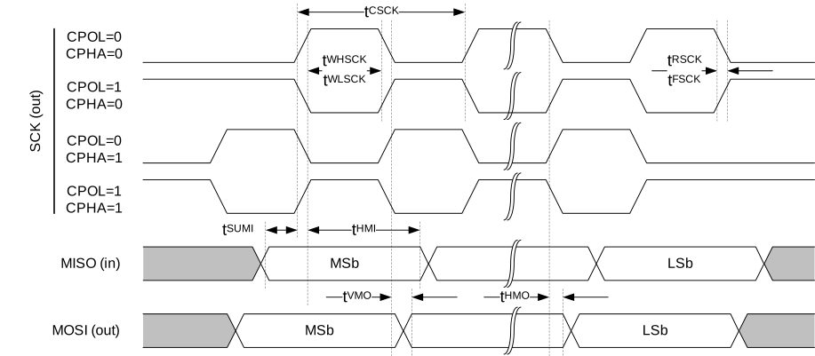
The SPIM does not implement support for chip select directly. Therefore, the CPU must use available GPIOs to select the correct slave and control this independently of the SPI master. The SPIM supports SPI modes 0 through 3. The CONFIG register allows setting CPOL and CPHA appropriately.
| Mode | Clock polarity | Clock phase |
|---|---|---|
| CPOL | CPHA | |
| SPI_MODE0 | 0 (Active High) | 0 (Leading) |
| SPI_MODE1 | 0 (Active High) | 1 (Trailing) |
| SPI_MODE2 | 1 (Active Low) | 0 (Leading) |
| SPI_MODE3 | 1 (Active Low) | 1 (Trailing) |
Shared resources
The SPI shares registers and other resources with other peripherals that have the same ID as the SPI. Therefore, the user must disable all peripherals that have the same ID as the SPI before the SPI can be configured and used.
Disabling a peripheral that has the same ID as the SPI will not reset any of the registers that are shared with the SPI. It is therefore important to configure all relevant SPI registers explicitly to secure that it operates correctly.
See the Instantiation table in Instantiation for details on peripherals and their IDs.
EasyDMA
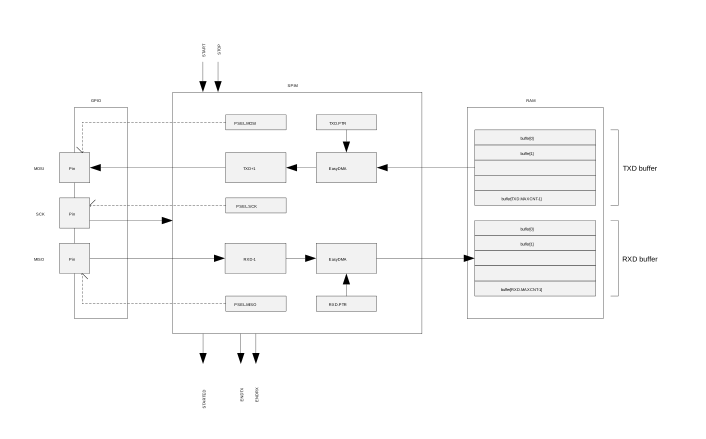
The SPI master implements EasyDMA for reading and writing of data packets from and to the DATA RAM without CPU involvement.
The RXD.PTR and TXD.PTR point to the RXD buffer (receive buffer) and TXD buffer (transmit buffer) respectively, see Figure 1. RXD.MAXCNT and TXD.MAXCNT specify the maximum number of bytes allocated to the buffers.
The SPI master will automatically stop transmitting after TXD.MAXCNT bytes have been transmitted and RXD.MAXCNT bytes have been received. If TXD.MAXCNT is larger than RXD.MAXCNT, the superfluous received bytes will be ignored. If RXD.MAXCNT is larger than TXD.MAXCNT, the remaining transmitted bytes will contain the value defined in the ORC register.
If the RXD.PTR and the TXD.PTR are not pointing to the Data RAM region, an EasyDMA transfer may result in a HardFault or RAM corruption. See Memory for more information about the different memory regions.
The .PTR and .MAXCNT registers are double-buffered. They can be updated and prepared for the next transmission immediately after having received the STARTED event.
The ENDRX/ENDTX event indicate that EasyDMA has finished accessing respectively the RX/TX buffer in RAM. The END event gets generated when both RX and TX are finished accessing the buffers in RAM.
EasyDMA list
EasyDMA supports one list type.
The supported list type is:
- Array list
EasyDMA array list
The EasyDMA array list can be represented by the data structure ArrayList_type.
For illustration, see the code example below. This data structure includes only a buffer with size equal to Channel.MAXCNT. EasyDMA will use the Channel.MAXCNT register to determine when the buffer is full. Replace 'Channel' by the specific data channel you want to use, for instance 'NRF_SPIM->RXD', 'NRF_SPIM->TXD', 'NRF_TWIM->RXD', etc.
The Channel.MAXCNT register cannot be specified larger than the actual size of the buffer. If Channel.MAXCNT is specified larger than the size of the buffer, the EasyDMA channel may overflow the buffer.
This array list does not provide a mechanism to explicitly specify where the next item in the list is located. Instead, it assumes that the list is organized as a linear array where items are located one after the other in RAM.
  #define BUFFER_SIZE  4

  typedef struct ArrayList
  {
    uint8_t buffer[BUFFER_SIZE];
  } ArrayList_type;

  ArrayList_type MyArrayList[3];

  //replace 'Channel' below by the specific data channel you want to use,
  //         for instance 'NRF_SPIM->RXD', 'NRF_TWIM->RXD', etc.
  Channel.MAXCNT = BUFFER_SIZE;
  Channel.PTR = &MyArrayList;

SPI master transaction sequence
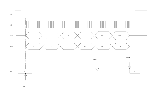
An SPI master transaction consists of a sequence started by the START task followed by a number of events, and finally the STOP task.
An SPI master transaction is started by triggering the START task. The ENDTX event will be generated when the transmitter has transmitted all bytes in the TXD buffer as specified in the TXD.MAXCNT register. The ENDRX event will be generated when the receiver has filled the RXD buffer, i.e. received the last possible byte as specified in the RXD.MAXCNT register.
Following a START task, the SPI master will generate an END event when both ENDRX and ENDTX have been generated.
The SPI master is stopped by triggering the STOP task. A STOPPED event is generated when the SPI master has stopped.
If the ENDRX event has not already been generated when the SPI master has come to a stop, the SPI master will generate the ENDRX event explicitly even though the RX buffer is not full.
If the ENDTX event has not already been generated when the SPI master has come to a stop, the SPI master will generate the ENDTX event explicitly even though all bytes in the TXD buffer, as specified in the TXD.MAXCNT register, have not been transmitted.
The SPI master is a synchronous interface, and for every byte that is sent, a different byte will be received at the same time; this is illustrated in Figure 3.
Low power
When putting the system in low power and the peripheral is not needed, lowest possible power consumption is achieved by stopping, and then disabling the peripheral.
The STOP task may not be always needed (the peripheral might already be stopped), but if it is sent, software shall wait until the STOPPED event was received as a response before disabling the peripheral through the ENABLE register.
Master mode pin configuration
The SCK, MOSI, and MISO signals associated with the SPI master are mapped to physical pins according to the configuration specified in the PSEL.SCK, PSEL.MOSI, and PSEL.MISO registers respectively.
The PSEL.SCK, PSEL.MOSI, and PSEL.MISO registers and their configurations are only used as long as the SPI master is enabled, and retained only as long as the device is in ON mode. PSEL.SCK, PSEL.MOSI and PSEL.MISO must only be configured when the SPI master is disabled.
To secure correct behavior in the SPI, the pins used by the SPI must be configured in the GPIO peripheral as described in Table 2 prior to enabling the SPI. This configuration must be retained in the GPIO for the selected IOs as long as the SPI is enabled.
Only one peripheral can be assigned to drive a particular GPIO pin at a time. Failing to do so may result in unpredictable behavior.
| SPI master signal | SPI master pin | Direction | Output value | Comments |
|---|---|---|---|---|
| SCK | As specified in PSEL.SCK | Output | Same as CONFIG.CPOL | |
| MOSI | As specified in PSEL.MOSI | Output | 0 | |
| MISO | As specified in PSEL.MISO | Input | Not applicable |
Registers
| Base address | Peripheral | Instance | Description | Configuration | |
|---|---|---|---|---|---|
| 0x40003000 | SPIM | SPIM0 | SPI master 0 | ||
| 0x40004000 | SPIM | SPIM1 | SPI master 1 | ||
| 0x40023000 | SPIM | SPIM2 | SPI master 2 | ||
| Register | Offset | Description | |
|---|---|---|---|
| TASKS_START | 0x010 | Start SPI transaction | |
| TASKS_STOP | 0x014 | Stop SPI transaction | |
| TASKS_SUSPEND | 0x01C | Suspend SPI transaction | |
| TASKS_RESUME | 0x020 | Resume SPI transaction | |
| EVENTS_STOPPED | 0x104 | SPI transaction has stopped | |
| EVENTS_ENDRX | 0x110 | End of RXD buffer reached | |
| EVENTS_END | 0x118 | End of RXD buffer and TXD buffer reached | |
| EVENTS_ENDTX | 0x120 | End of TXD buffer reached | |
| EVENTS_STARTED | 0x14C | Transaction started | |
| SHORTS | 0x200 | Shortcut register | |
| INTENSET | 0x304 | Enable interrupt | |
| INTENCLR | 0x308 | Disable interrupt | |
| ENABLE | 0x500 | Enable SPIM | |
| PSEL.SCK | 0x508 | Pin select for SCK | |
| PSEL.MOSI | 0x50C | Pin select for MOSI signal | |
| PSEL.MISO | 0x510 | Pin select for MISO signal | |
| FREQUENCY | 0x524 | SPI frequency. Accuracy depends on the HFCLK source selected. | |
| RXD.PTR | 0x534 | Data pointer | |
| RXD.MAXCNT | 0x538 | Maximum number of bytes in receive buffer | |
| RXD.AMOUNT | 0x53C | Number of bytes transferred in the last transaction | |
| RXD.LIST | 0x540 | EasyDMA list type | |
| TXD.PTR | 0x544 | Data pointer | |
| TXD.MAXCNT | 0x548 | Maximum number of bytes in transmit buffer | |
| TXD.AMOUNT | 0x54C | Number of bytes transferred in the last transaction | |
| TXD.LIST | 0x550 | EasyDMA list type | |
| CONFIG | 0x554 | Configuration register | |
| ORC | 0x5C0 | Over-read character. Character clocked out in case and over-read of the TXD buffer. | |
SHORTS
Address offset: 0x200
Shortcut register
| Bit number | 31 | 30 | 29 | 28 | 27 | 26 | 25 | 24 | 23 | 22 | 21 | 20 | 19 | 18 | 17 | 16 | 15 | 14 | 13 | 12 | 11 | 10 | 9 | 8 | 7 | 6 | 5 | 4 | 3 | 2 | 1 | 0 | |||
|---|---|---|---|---|---|---|---|---|---|---|---|---|---|---|---|---|---|---|---|---|---|---|---|---|---|---|---|---|---|---|---|---|---|---|---|
| Id | A | ||||||||||||||||||||||||||||||||||
| Reset 0x00000000 | 0 | 0 | 0 | 0 | 0 | 0 | 0 | 0 | 0 | 0 | 0 | 0 | 0 | 0 | 0 | 0 | 0 | 0 | 0 | 0 | 0 | 0 | 0 | 0 | 0 | 0 | 0 | 0 | 0 | 0 | 0 | 0 | |||
| Id | RW | Field | Value Id | Value | Description | ||||||||||||||||||||||||||||||
| A | RW | END_START | Shortcut between END event and START task See EVENTS_END and TASKS_START | ||||||||||||||||||||||||||||||||
Disabled | 0 | Disable shortcut | |||||||||||||||||||||||||||||||||
Enabled | 1 | Enable shortcut | |||||||||||||||||||||||||||||||||
INTENSET
Address offset: 0x304
Enable interrupt
| Bit number | 31 | 30 | 29 | 28 | 27 | 26 | 25 | 24 | 23 | 22 | 21 | 20 | 19 | 18 | 17 | 16 | 15 | 14 | 13 | 12 | 11 | 10 | 9 | 8 | 7 | 6 | 5 | 4 | 3 | 2 | 1 | 0 | |||
|---|---|---|---|---|---|---|---|---|---|---|---|---|---|---|---|---|---|---|---|---|---|---|---|---|---|---|---|---|---|---|---|---|---|---|---|
| Id | E | D | C | B | A | ||||||||||||||||||||||||||||||
| Reset 0x00000000 | 0 | 0 | 0 | 0 | 0 | 0 | 0 | 0 | 0 | 0 | 0 | 0 | 0 | 0 | 0 | 0 | 0 | 0 | 0 | 0 | 0 | 0 | 0 | 0 | 0 | 0 | 0 | 0 | 0 | 0 | 0 | 0 | |||
| Id | RW | Field | Value Id | Value | Description | ||||||||||||||||||||||||||||||
| A | RW | STOPPED | Write '1' to Enable interrupt for STOPPED event See EVENTS_STOPPED | ||||||||||||||||||||||||||||||||
Set | 1 | Enable | |||||||||||||||||||||||||||||||||
Disabled | 0 | Read: Disabled | |||||||||||||||||||||||||||||||||
Enabled | 1 | Read: Enabled | |||||||||||||||||||||||||||||||||
| B | RW | ENDRX | Write '1' to Enable interrupt for ENDRX event See EVENTS_ENDRX | ||||||||||||||||||||||||||||||||
Set | 1 | Enable | |||||||||||||||||||||||||||||||||
Disabled | 0 | Read: Disabled | |||||||||||||||||||||||||||||||||
Enabled | 1 | Read: Enabled | |||||||||||||||||||||||||||||||||
| C | RW | END | Write '1' to Enable interrupt for END event See EVENTS_END | ||||||||||||||||||||||||||||||||
Set | 1 | Enable | |||||||||||||||||||||||||||||||||
Disabled | 0 | Read: Disabled | |||||||||||||||||||||||||||||||||
Enabled | 1 | Read: Enabled | |||||||||||||||||||||||||||||||||
| D | RW | ENDTX | Write '1' to Enable interrupt for ENDTX event See EVENTS_ENDTX | ||||||||||||||||||||||||||||||||
Set | 1 | Enable | |||||||||||||||||||||||||||||||||
Disabled | 0 | Read: Disabled | |||||||||||||||||||||||||||||||||
Enabled | 1 | Read: Enabled | |||||||||||||||||||||||||||||||||
| E | RW | STARTED | Write '1' to Enable interrupt for STARTED event See EVENTS_STARTED | ||||||||||||||||||||||||||||||||
Set | 1 | Enable | |||||||||||||||||||||||||||||||||
Disabled | 0 | Read: Disabled | |||||||||||||||||||||||||||||||||
Enabled | 1 | Read: Enabled | |||||||||||||||||||||||||||||||||
INTENCLR
Address offset: 0x308
Disable interrupt
| Bit number | 31 | 30 | 29 | 28 | 27 | 26 | 25 | 24 | 23 | 22 | 21 | 20 | 19 | 18 | 17 | 16 | 15 | 14 | 13 | 12 | 11 | 10 | 9 | 8 | 7 | 6 | 5 | 4 | 3 | 2 | 1 | 0 | |||
|---|---|---|---|---|---|---|---|---|---|---|---|---|---|---|---|---|---|---|---|---|---|---|---|---|---|---|---|---|---|---|---|---|---|---|---|
| Id | E | D | C | B | A | ||||||||||||||||||||||||||||||
| Reset 0x00000000 | 0 | 0 | 0 | 0 | 0 | 0 | 0 | 0 | 0 | 0 | 0 | 0 | 0 | 0 | 0 | 0 | 0 | 0 | 0 | 0 | 0 | 0 | 0 | 0 | 0 | 0 | 0 | 0 | 0 | 0 | 0 | 0 | |||
| Id | RW | Field | Value Id | Value | Description | ||||||||||||||||||||||||||||||
| A | RW | STOPPED | Write '1' to Disable interrupt for STOPPED event See EVENTS_STOPPED | ||||||||||||||||||||||||||||||||
Clear | 1 | Disable | |||||||||||||||||||||||||||||||||
Disabled | 0 | Read: Disabled | |||||||||||||||||||||||||||||||||
Enabled | 1 | Read: Enabled | |||||||||||||||||||||||||||||||||
| B | RW | ENDRX | Write '1' to Disable interrupt for ENDRX event See EVENTS_ENDRX | ||||||||||||||||||||||||||||||||
Clear | 1 | Disable | |||||||||||||||||||||||||||||||||
Disabled | 0 | Read: Disabled | |||||||||||||||||||||||||||||||||
Enabled | 1 | Read: Enabled | |||||||||||||||||||||||||||||||||
| C | RW | END | Write '1' to Disable interrupt for END event See EVENTS_END | ||||||||||||||||||||||||||||||||
Clear | 1 | Disable | |||||||||||||||||||||||||||||||||
Disabled | 0 | Read: Disabled | |||||||||||||||||||||||||||||||||
Enabled | 1 | Read: Enabled | |||||||||||||||||||||||||||||||||
| D | RW | ENDTX | Write '1' to Disable interrupt for ENDTX event See EVENTS_ENDTX | ||||||||||||||||||||||||||||||||
Clear | 1 | Disable | |||||||||||||||||||||||||||||||||
Disabled | 0 | Read: Disabled | |||||||||||||||||||||||||||||||||
Enabled | 1 | Read: Enabled | |||||||||||||||||||||||||||||||||
| E | RW | STARTED | Write '1' to Disable interrupt for STARTED event See EVENTS_STARTED | ||||||||||||||||||||||||||||||||
Clear | 1 | Disable | |||||||||||||||||||||||||||||||||
Disabled | 0 | Read: Disabled | |||||||||||||||||||||||||||||||||
Enabled | 1 | Read: Enabled | |||||||||||||||||||||||||||||||||
ENABLE
Address offset: 0x500
Enable SPIM
| Bit number | 31 | 30 | 29 | 28 | 27 | 26 | 25 | 24 | 23 | 22 | 21 | 20 | 19 | 18 | 17 | 16 | 15 | 14 | 13 | 12 | 11 | 10 | 9 | 8 | 7 | 6 | 5 | 4 | 3 | 2 | 1 | 0 | |||
|---|---|---|---|---|---|---|---|---|---|---|---|---|---|---|---|---|---|---|---|---|---|---|---|---|---|---|---|---|---|---|---|---|---|---|---|
| Id | A | A | A | A | |||||||||||||||||||||||||||||||
| Reset 0x00000000 | 0 | 0 | 0 | 0 | 0 | 0 | 0 | 0 | 0 | 0 | 0 | 0 | 0 | 0 | 0 | 0 | 0 | 0 | 0 | 0 | 0 | 0 | 0 | 0 | 0 | 0 | 0 | 0 | 0 | 0 | 0 | 0 | |||
| Id | RW | Field | Value Id | Value | Description | ||||||||||||||||||||||||||||||
| A | RW | ENABLE | Enable or disable SPIM | ||||||||||||||||||||||||||||||||
Disabled | 0 | Disable SPIM | |||||||||||||||||||||||||||||||||
Enabled | 7 | Enable SPIM | |||||||||||||||||||||||||||||||||
PSEL.SCK
Address offset: 0x508
Pin select for SCK
| Bit number | 31 | 30 | 29 | 28 | 27 | 26 | 25 | 24 | 23 | 22 | 21 | 20 | 19 | 18 | 17 | 16 | 15 | 14 | 13 | 12 | 11 | 10 | 9 | 8 | 7 | 6 | 5 | 4 | 3 | 2 | 1 | 0 | |||
|---|---|---|---|---|---|---|---|---|---|---|---|---|---|---|---|---|---|---|---|---|---|---|---|---|---|---|---|---|---|---|---|---|---|---|---|
| Id | C | A | A | A | A | A | |||||||||||||||||||||||||||||
| Reset 0xFFFFFFFF | 1 | 1 | 1 | 1 | 1 | 1 | 1 | 1 | 1 | 1 | 1 | 1 | 1 | 1 | 1 | 1 | 1 | 1 | 1 | 1 | 1 | 1 | 1 | 1 | 1 | 1 | 1 | 1 | 1 | 1 | 1 | 1 | |||
| Id | RW | Field | Value Id | Value | Description | ||||||||||||||||||||||||||||||
| A | RW | PIN | [0..31] | Pin number | |||||||||||||||||||||||||||||||
| C | RW | CONNECT | Connection | ||||||||||||||||||||||||||||||||
Disconnected | 1 | Disconnect | |||||||||||||||||||||||||||||||||
Connected | 0 | Connect | |||||||||||||||||||||||||||||||||
PSEL.MOSI
Address offset: 0x50C
Pin select for MOSI signal
| Bit number | 31 | 30 | 29 | 28 | 27 | 26 | 25 | 24 | 23 | 22 | 21 | 20 | 19 | 18 | 17 | 16 | 15 | 14 | 13 | 12 | 11 | 10 | 9 | 8 | 7 | 6 | 5 | 4 | 3 | 2 | 1 | 0 | |||
|---|---|---|---|---|---|---|---|---|---|---|---|---|---|---|---|---|---|---|---|---|---|---|---|---|---|---|---|---|---|---|---|---|---|---|---|
| Id | C | A | A | A | A | A | |||||||||||||||||||||||||||||
| Reset 0xFFFFFFFF | 1 | 1 | 1 | 1 | 1 | 1 | 1 | 1 | 1 | 1 | 1 | 1 | 1 | 1 | 1 | 1 | 1 | 1 | 1 | 1 | 1 | 1 | 1 | 1 | 1 | 1 | 1 | 1 | 1 | 1 | 1 | 1 | |||
| Id | RW | Field | Value Id | Value | Description | ||||||||||||||||||||||||||||||
| A | RW | PIN | [0..31] | Pin number | |||||||||||||||||||||||||||||||
| C | RW | CONNECT | Connection | ||||||||||||||||||||||||||||||||
Disconnected | 1 | Disconnect | |||||||||||||||||||||||||||||||||
Connected | 0 | Connect | |||||||||||||||||||||||||||||||||
PSEL.MISO
Address offset: 0x510
Pin select for MISO signal
| Bit number | 31 | 30 | 29 | 28 | 27 | 26 | 25 | 24 | 23 | 22 | 21 | 20 | 19 | 18 | 17 | 16 | 15 | 14 | 13 | 12 | 11 | 10 | 9 | 8 | 7 | 6 | 5 | 4 | 3 | 2 | 1 | 0 | |||
|---|---|---|---|---|---|---|---|---|---|---|---|---|---|---|---|---|---|---|---|---|---|---|---|---|---|---|---|---|---|---|---|---|---|---|---|
| Id | C | A | A | A | A | A | |||||||||||||||||||||||||||||
| Reset 0xFFFFFFFF | 1 | 1 | 1 | 1 | 1 | 1 | 1 | 1 | 1 | 1 | 1 | 1 | 1 | 1 | 1 | 1 | 1 | 1 | 1 | 1 | 1 | 1 | 1 | 1 | 1 | 1 | 1 | 1 | 1 | 1 | 1 | 1 | |||
| Id | RW | Field | Value Id | Value | Description | ||||||||||||||||||||||||||||||
| A | RW | PIN | [0..31] | Pin number | |||||||||||||||||||||||||||||||
| C | RW | CONNECT | Connection | ||||||||||||||||||||||||||||||||
Disconnected | 1 | Disconnect | |||||||||||||||||||||||||||||||||
Connected | 0 | Connect | |||||||||||||||||||||||||||||||||
FREQUENCY
Address offset: 0x524
SPI frequency. Accuracy depends on the HFCLK source selected.
| Bit number | 31 | 30 | 29 | 28 | 27 | 26 | 25 | 24 | 23 | 22 | 21 | 20 | 19 | 18 | 17 | 16 | 15 | 14 | 13 | 12 | 11 | 10 | 9 | 8 | 7 | 6 | 5 | 4 | 3 | 2 | 1 | 0 | |||
|---|---|---|---|---|---|---|---|---|---|---|---|---|---|---|---|---|---|---|---|---|---|---|---|---|---|---|---|---|---|---|---|---|---|---|---|
| Id | A | A | A | A | A | A | A | A | A | A | A | A | A | A | A | A | A | A | A | A | A | A | A | A | A | A | A | A | A | A | A | A | |||
| Reset 0x04000000 | 0 | 0 | 0 | 0 | 0 | 1 | 0 | 0 | 0 | 0 | 0 | 0 | 0 | 0 | 0 | 0 | 0 | 0 | 0 | 0 | 0 | 0 | 0 | 0 | 0 | 0 | 0 | 0 | 0 | 0 | 0 | 0 | |||
| Id | RW | Field | Value Id | Value | Description | ||||||||||||||||||||||||||||||
| A | RW | FREQUENCY | SPI master data rate | ||||||||||||||||||||||||||||||||
K125 | 0x02000000 | 125 kbps | |||||||||||||||||||||||||||||||||
K250 | 0x04000000 | 250 kbps | |||||||||||||||||||||||||||||||||
K500 | 0x08000000 | 500 kbps | |||||||||||||||||||||||||||||||||
M1 | 0x10000000 | 1 Mbps | |||||||||||||||||||||||||||||||||
M2 | 0x20000000 | 2 Mbps | |||||||||||||||||||||||||||||||||
M4 | 0x40000000 | 4 Mbps | |||||||||||||||||||||||||||||||||
M8 | 0x80000000 | 8 Mbps | |||||||||||||||||||||||||||||||||
RXD.PTR
Address offset: 0x534
Data pointer
| Bit number | 31 | 30 | 29 | 28 | 27 | 26 | 25 | 24 | 23 | 22 | 21 | 20 | 19 | 18 | 17 | 16 | 15 | 14 | 13 | 12 | 11 | 10 | 9 | 8 | 7 | 6 | 5 | 4 | 3 | 2 | 1 | 0 | |||
|---|---|---|---|---|---|---|---|---|---|---|---|---|---|---|---|---|---|---|---|---|---|---|---|---|---|---|---|---|---|---|---|---|---|---|---|
| Id | A | A | A | A | A | A | A | A | A | A | A | A | A | A | A | A | A | A | A | A | A | A | A | A | A | A | A | A | A | A | A | A | |||
| Reset 0x00000000 | 0 | 0 | 0 | 0 | 0 | 0 | 0 | 0 | 0 | 0 | 0 | 0 | 0 | 0 | 0 | 0 | 0 | 0 | 0 | 0 | 0 | 0 | 0 | 0 | 0 | 0 | 0 | 0 | 0 | 0 | 0 | 0 | |||
| Id | RW | Field | Value Id | Value | Description | ||||||||||||||||||||||||||||||
| A | RW | PTR | Data pointer | ||||||||||||||||||||||||||||||||
RXD.MAXCNT
Address offset: 0x538
Maximum number of bytes in receive buffer
| Bit number | 31 | 30 | 29 | 28 | 27 | 26 | 25 | 24 | 23 | 22 | 21 | 20 | 19 | 18 | 17 | 16 | 15 | 14 | 13 | 12 | 11 | 10 | 9 | 8 | 7 | 6 | 5 | 4 | 3 | 2 | 1 | 0 | |||
|---|---|---|---|---|---|---|---|---|---|---|---|---|---|---|---|---|---|---|---|---|---|---|---|---|---|---|---|---|---|---|---|---|---|---|---|
| Id | A | A | A | A | A | A | A | A | |||||||||||||||||||||||||||
| Reset 0x00000000 | 0 | 0 | 0 | 0 | 0 | 0 | 0 | 0 | 0 | 0 | 0 | 0 | 0 | 0 | 0 | 0 | 0 | 0 | 0 | 0 | 0 | 0 | 0 | 0 | 0 | 0 | 0 | 0 | 0 | 0 | 0 | 0 | |||
| Id | RW | Field | Value Id | Value | Description | ||||||||||||||||||||||||||||||
| A | RW | MAXCNT | Maximum number of bytes in receive buffer | ||||||||||||||||||||||||||||||||
RXD.AMOUNT
Address offset: 0x53C
Number of bytes transferred in the last transaction
| Bit number | 31 | 30 | 29 | 28 | 27 | 26 | 25 | 24 | 23 | 22 | 21 | 20 | 19 | 18 | 17 | 16 | 15 | 14 | 13 | 12 | 11 | 10 | 9 | 8 | 7 | 6 | 5 | 4 | 3 | 2 | 1 | 0 | |||
|---|---|---|---|---|---|---|---|---|---|---|---|---|---|---|---|---|---|---|---|---|---|---|---|---|---|---|---|---|---|---|---|---|---|---|---|
| Id | A | A | A | A | A | A | A | A | |||||||||||||||||||||||||||
| Reset 0x00000000 | 0 | 0 | 0 | 0 | 0 | 0 | 0 | 0 | 0 | 0 | 0 | 0 | 0 | 0 | 0 | 0 | 0 | 0 | 0 | 0 | 0 | 0 | 0 | 0 | 0 | 0 | 0 | 0 | 0 | 0 | 0 | 0 | |||
| Id | RW | Field | Value Id | Value | Description | ||||||||||||||||||||||||||||||
| A | R | AMOUNT | Number of bytes transferred in the last transaction | ||||||||||||||||||||||||||||||||
RXD.LIST
Address offset: 0x540
EasyDMA list type
| Bit number | 31 | 30 | 29 | 28 | 27 | 26 | 25 | 24 | 23 | 22 | 21 | 20 | 19 | 18 | 17 | 16 | 15 | 14 | 13 | 12 | 11 | 10 | 9 | 8 | 7 | 6 | 5 | 4 | 3 | 2 | 1 | 0 | |||
|---|---|---|---|---|---|---|---|---|---|---|---|---|---|---|---|---|---|---|---|---|---|---|---|---|---|---|---|---|---|---|---|---|---|---|---|
| Id | A | A | A | ||||||||||||||||||||||||||||||||
| Reset 0x00000000 | 0 | 0 | 0 | 0 | 0 | 0 | 0 | 0 | 0 | 0 | 0 | 0 | 0 | 0 | 0 | 0 | 0 | 0 | 0 | 0 | 0 | 0 | 0 | 0 | 0 | 0 | 0 | 0 | 0 | 0 | 0 | 0 | |||
| Id | RW | Field | Value Id | Value | Description | ||||||||||||||||||||||||||||||
| A | RW | LIST | List type | ||||||||||||||||||||||||||||||||
Disabled | 0 | Disable EasyDMA list | |||||||||||||||||||||||||||||||||
ArrayList | 1 | Use array list | |||||||||||||||||||||||||||||||||
TXD.PTR
Address offset: 0x544
Data pointer
| Bit number | 31 | 30 | 29 | 28 | 27 | 26 | 25 | 24 | 23 | 22 | 21 | 20 | 19 | 18 | 17 | 16 | 15 | 14 | 13 | 12 | 11 | 10 | 9 | 8 | 7 | 6 | 5 | 4 | 3 | 2 | 1 | 0 | |||
|---|---|---|---|---|---|---|---|---|---|---|---|---|---|---|---|---|---|---|---|---|---|---|---|---|---|---|---|---|---|---|---|---|---|---|---|
| Id | A | A | A | A | A | A | A | A | A | A | A | A | A | A | A | A | A | A | A | A | A | A | A | A | A | A | A | A | A | A | A | A | |||
| Reset 0x00000000 | 0 | 0 | 0 | 0 | 0 | 0 | 0 | 0 | 0 | 0 | 0 | 0 | 0 | 0 | 0 | 0 | 0 | 0 | 0 | 0 | 0 | 0 | 0 | 0 | 0 | 0 | 0 | 0 | 0 | 0 | 0 | 0 | |||
| Id | RW | Field | Value Id | Value | Description | ||||||||||||||||||||||||||||||
| A | RW | PTR | Data pointer | ||||||||||||||||||||||||||||||||
TXD.MAXCNT
Address offset: 0x548
Maximum number of bytes in transmit buffer
| Bit number | 31 | 30 | 29 | 28 | 27 | 26 | 25 | 24 | 23 | 22 | 21 | 20 | 19 | 18 | 17 | 16 | 15 | 14 | 13 | 12 | 11 | 10 | 9 | 8 | 7 | 6 | 5 | 4 | 3 | 2 | 1 | 0 | |||
|---|---|---|---|---|---|---|---|---|---|---|---|---|---|---|---|---|---|---|---|---|---|---|---|---|---|---|---|---|---|---|---|---|---|---|---|
| Id | A | A | A | A | A | A | A | A | |||||||||||||||||||||||||||
| Reset 0x00000000 | 0 | 0 | 0 | 0 | 0 | 0 | 0 | 0 | 0 | 0 | 0 | 0 | 0 | 0 | 0 | 0 | 0 | 0 | 0 | 0 | 0 | 0 | 0 | 0 | 0 | 0 | 0 | 0 | 0 | 0 | 0 | 0 | |||
| Id | RW | Field | Value Id | Value | Description | ||||||||||||||||||||||||||||||
| A | RW | MAXCNT | Maximum number of bytes in transmit buffer | ||||||||||||||||||||||||||||||||
TXD.AMOUNT
Address offset: 0x54C
Number of bytes transferred in the last transaction
| Bit number | 31 | 30 | 29 | 28 | 27 | 26 | 25 | 24 | 23 | 22 | 21 | 20 | 19 | 18 | 17 | 16 | 15 | 14 | 13 | 12 | 11 | 10 | 9 | 8 | 7 | 6 | 5 | 4 | 3 | 2 | 1 | 0 | |||
|---|---|---|---|---|---|---|---|---|---|---|---|---|---|---|---|---|---|---|---|---|---|---|---|---|---|---|---|---|---|---|---|---|---|---|---|
| Id | A | A | A | A | A | A | A | A | |||||||||||||||||||||||||||
| Reset 0x00000000 | 0 | 0 | 0 | 0 | 0 | 0 | 0 | 0 | 0 | 0 | 0 | 0 | 0 | 0 | 0 | 0 | 0 | 0 | 0 | 0 | 0 | 0 | 0 | 0 | 0 | 0 | 0 | 0 | 0 | 0 | 0 | 0 | |||
| Id | RW | Field | Value Id | Value | Description | ||||||||||||||||||||||||||||||
| A | R | AMOUNT | Number of bytes transferred in the last transaction | ||||||||||||||||||||||||||||||||
TXD.LIST
Address offset: 0x550
EasyDMA list type
| Bit number | 31 | 30 | 29 | 28 | 27 | 26 | 25 | 24 | 23 | 22 | 21 | 20 | 19 | 18 | 17 | 16 | 15 | 14 | 13 | 12 | 11 | 10 | 9 | 8 | 7 | 6 | 5 | 4 | 3 | 2 | 1 | 0 | |||
|---|---|---|---|---|---|---|---|---|---|---|---|---|---|---|---|---|---|---|---|---|---|---|---|---|---|---|---|---|---|---|---|---|---|---|---|
| Id | A | A | A | ||||||||||||||||||||||||||||||||
| Reset 0x00000000 | 0 | 0 | 0 | 0 | 0 | 0 | 0 | 0 | 0 | 0 | 0 | 0 | 0 | 0 | 0 | 0 | 0 | 0 | 0 | 0 | 0 | 0 | 0 | 0 | 0 | 0 | 0 | 0 | 0 | 0 | 0 | 0 | |||
| Id | RW | Field | Value Id | Value | Description | ||||||||||||||||||||||||||||||
| A | RW | LIST | List type | ||||||||||||||||||||||||||||||||
Disabled | 0 | Disable EasyDMA list | |||||||||||||||||||||||||||||||||
ArrayList | 1 | Use array list | |||||||||||||||||||||||||||||||||
CONFIG
Address offset: 0x554
Configuration register
| Bit number | 31 | 30 | 29 | 28 | 27 | 26 | 25 | 24 | 23 | 22 | 21 | 20 | 19 | 18 | 17 | 16 | 15 | 14 | 13 | 12 | 11 | 10 | 9 | 8 | 7 | 6 | 5 | 4 | 3 | 2 | 1 | 0 | |||
|---|---|---|---|---|---|---|---|---|---|---|---|---|---|---|---|---|---|---|---|---|---|---|---|---|---|---|---|---|---|---|---|---|---|---|---|
| Id | C | B | A | ||||||||||||||||||||||||||||||||
| Reset 0x00000000 | 0 | 0 | 0 | 0 | 0 | 0 | 0 | 0 | 0 | 0 | 0 | 0 | 0 | 0 | 0 | 0 | 0 | 0 | 0 | 0 | 0 | 0 | 0 | 0 | 0 | 0 | 0 | 0 | 0 | 0 | 0 | 0 | |||
| Id | RW | Field | Value Id | Value | Description | ||||||||||||||||||||||||||||||
| A | RW | ORDER | Bit order | ||||||||||||||||||||||||||||||||
MsbFirst | 0 | Most significant bit shifted out first | |||||||||||||||||||||||||||||||||
LsbFirst | 1 | Least significant bit shifted out first | |||||||||||||||||||||||||||||||||
| B | RW | CPHA | Serial clock (SCK) phase | ||||||||||||||||||||||||||||||||
Leading | 0 | Sample on leading edge of clock, shift serial data on trailing edge | |||||||||||||||||||||||||||||||||
Trailing | 1 | Sample on trailing edge of clock, shift serial data on leading edge | |||||||||||||||||||||||||||||||||
| C | RW | CPOL | Serial clock (SCK) polarity | ||||||||||||||||||||||||||||||||
ActiveHigh | 0 | Active high | |||||||||||||||||||||||||||||||||
ActiveLow | 1 | Active low | |||||||||||||||||||||||||||||||||
ORC
Address offset: 0x5C0
Over-read character. Character clocked out in case and over-read of the TXD buffer.
| Bit number | 31 | 30 | 29 | 28 | 27 | 26 | 25 | 24 | 23 | 22 | 21 | 20 | 19 | 18 | 17 | 16 | 15 | 14 | 13 | 12 | 11 | 10 | 9 | 8 | 7 | 6 | 5 | 4 | 3 | 2 | 1 | 0 | |||
|---|---|---|---|---|---|---|---|---|---|---|---|---|---|---|---|---|---|---|---|---|---|---|---|---|---|---|---|---|---|---|---|---|---|---|---|
| Id | A | A | A | A | A | A | A | A | |||||||||||||||||||||||||||
| Reset 0x00000000 | 0 | 0 | 0 | 0 | 0 | 0 | 0 | 0 | 0 | 0 | 0 | 0 | 0 | 0 | 0 | 0 | 0 | 0 | 0 | 0 | 0 | 0 | 0 | 0 | 0 | 0 | 0 | 0 | 0 | 0 | 0 | 0 | |||
| Id | RW | Field | Value Id | Value | Description | ||||||||||||||||||||||||||||||
| A | RW | ORC | Over-read character. Character clocked out in case and over-read of the TXD buffer. | ||||||||||||||||||||||||||||||||
Electrical specification
SPIM master interface electrical specifications
Serial Peripheral Interface Master (SPIM) timing specifications
| Symbol | Description | Min. | Typ. | Max. | Units | ||||
|---|---|---|---|---|---|---|---|---|---|
| tSPIM,CSCK | SCK period | .. | .. | .. | ns | ||||
| tSPIM,RSCK,LD | SCK rise time, standard drivea | tRF,25pF | |||||||
| tSPIM,RSCK,HD | SCK rise time, high drivea | tHRF,25pF | |||||||
| tSPIM,FSCK,LD | SCK fall time, standard drivea | tRF,25pF | |||||||
| tSPIM,FSCK,HD | SCK fall time, high drivea | tHRF,25pF | |||||||
| tSPIM,WHSCK | SCK high timea | (0.5*tCSCK) – tRSCK | |||||||
| tSPIM,WLSCK | SCK low timea | (0.5*tCSCK) – tFSCK | |||||||
| tSPIM,SUMI | MISO to CLK edge setup time | 19 | ns | ||||||
| tSPIM,HMI | CLK edge to MISO hold time | 18 | ns | ||||||
| tSPIM,VMO | CLK edge to MOSI valid | 59 | ns | ||||||
| tSPIM,HMO | MOSI hold time after CLK edge | 20 | ns |