SPIS — Serial peripheral interface slave with EasyDMA
SPI slave (SPIS) is implemented with EasyDMA support for ultra low power serial communication from an external SPI master. EasyDMA in conjunction with hardware-based semaphore mechanisms removes all real-time requirements associated with controlling the SPI slave from a low priority CPU execution context.
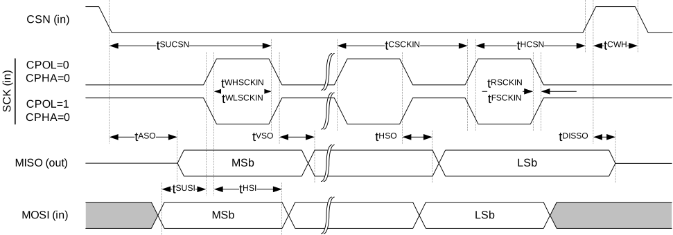
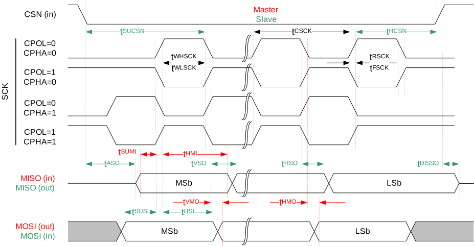
The SPIS supports SPI modes 0 through 3. The CONFIG register allows setting CPOL and CPHA appropriately.
| Mode | Clock polarity | Clock phase |
|---|---|---|
| CPOL | CPHA | |
| SPI_MODE0 | 0 (Leading) | 0 (Active High) |
| SPI_MODE1 | 0 (Leading) | 1 (Active Low) |
| SPI_MODE2 | 1 (Trailing) | 0 (Active High) |
| SPI_MODE3 | 1 (Trailing) | 1 (Active Low) |
Shared resources
The SPI slave shares registers and other resources with other peripherals that have the same ID as the SPI slave. Therefore, you must disable all peripherals that have the same ID as the SPI slave before the SPI slave can be configured and used.
Disabling a peripheral that has the same ID as the SPI slave will not reset any of the registers that are shared with the SPI slave. It is important to configure all relevant SPI slave registers explicitly to secure that it operates correctly.
The Instantiation table in Instantiation shows which peripherals have the same ID as the SPI slave.
EasyDMA
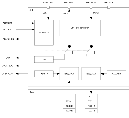
The SPI slave implements EasyDMA for reading and writing to and from the RAM. The END event indicates that EasyDMA has finished accessing the buffer in RAM.
If the TXD.PTR and the RXD.PTR are not pointing to the Data RAM region, an EasyDMA transfer may result in a HardFault or RAM corruption. See Memory for more information about the different memory regions.
SPI slave operation
SPI slave uses two memory pointers, RXD.PTR and TXD.PTR, that point to the RXD buffer (receive buffer) and TXD buffer (transmit buffer) respectively. Since these buffers are located in RAM, which can be accessed by both the SPI slave and the CPU, a hardware based semaphore mechanism is implemented to enable safe sharing.
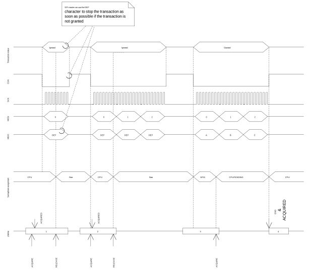
See Figure 2.
Before the CPU can safely update the RXD.PTR and TXD.PTR pointers it must first acquire the SPI semaphore. The CPU can acquire the semaphore by triggering the ACQUIRE task and then receiving the ACQUIRED event. When the CPU has updated the RXD.PTR and TXD.PTR pointers the CPU must release the semaphore before the SPI slave will be able to acquire it. The CPU releases the semaphore by triggering the RELEASE task. This is illustrated in Figure 2. Triggering the RELEASE task when the semaphore is not granted to the CPU will have no effect.
The semaphore mechanism does not, at any time, prevent the CPU from performing read or write access to the RXD.PTR register, the TXD.PTR registers, or the RAM that these pointers are pointing to. The semaphore is only telling when these can be updated by the CPU so that safe sharing is achieved.
The semaphore is by default assigned to the CPU after the SPI slave is enabled. No ACQUIRED event will be generated for this initial semaphore handover. An ACQUIRED event will be generated immediately if the ACQUIRE task is triggered while the semaphore is assigned to the CPU.
The SPI slave will try to acquire the semaphore when CSN goes low. If the SPI slave does not manage to acquire the semaphore at this point, the transaction will be ignored. This means that all incoming data on MOSI will be discarded, and the DEF (default) character will be clocked out on the MISO line throughout the whole transaction. This will also be the case even if the semaphore is released by the CPU during the transaction. In case of a race condition where the CPU and the SPI slave try to acquire the semaphore at the same time, as illustrated in lifeline item 2 in Figure 2, the semaphore will be granted to the CPU.
If the SPI slave acquires the semaphore, the transaction will be granted. The incoming data on MOSI will be stored in the RXD buffer and the data in the TXD buffer will be clocked out on MISO.
When a granted transaction is completed and CSN goes high, the SPI slave will automatically release the semaphore and generate the END event.
As long as the semaphore is available the SPI slave can be granted multiple transactions one after the other. If the CPU is not able to reconfigure the TXD.PTR and RXD.PTR between granted transactions, the same TX data will be clocked out and the RX buffers will be overwritten. To prevent this from happening, the END_ACQUIRE shortcut can be used. With this shortcut enabled the semaphore will be handed over to the CPU automatically after the granted transaction has completed, giving the CPU the ability to update the TXPTR and RXPTR between every granted transaction.
If the CPU tries to acquire the semaphore while it is assigned to the SPI slave, an immediate handover will not be granted. However, the semaphore will be handed over to the CPU as soon as the SPI slave has released the semaphore after the granted transaction is completed. If the END_ACQUIRE shortcut is enabled and the CPU has triggered the ACQUIRE task during a granted transaction, only one ACQUIRE request will be served following the END event.
The MAXRX register specifies the maximum number of bytes the SPI slave can receive in one granted transaction. If the SPI slave receives more than MAXRX number of bytes, an OVERFLOW will be indicated in the STATUS register and the incoming bytes will be discarded.
The MAXTX parameter specifies the maximum number of bytes the SPI slave can transmit in one granted transaction. If the SPI slave is forced to transmit more than MAXTX number of bytes, an OVERREAD will be indicated in the STATUS register and the ORC character will be clocked out.
The RXD.AMOUNT and TXD.AMOUNT registers are updated when a granted transaction is completed. The TXD.AMOUNT register indicates how many bytes were read from the TX buffer in the last transaction, that is, ORC (over-read) characters are not included in this number. Similarly, the RXD.AMOUNT register indicates how many bytes were written into the RX buffer in the last transaction.
The ENDRX event is generated when the RX buffer has been filled.
Pin configuration
The CSN, SCK, MOSI, and MISO signals associated with the SPI slave are mapped to physical pins according to the configuration specified in the PSEL.CSN, PSEL.SCK, PSEL.MOSI, and PSEL.MISO registers respectively. If the CONNECT field of any of these registers is set to Disconnected, the associated SPI slave signal will not be connected to any physical pins.
The PSEL.CSN, PSEL.SCK, PSEL.MOSI, and PSEL.MISO registers and their configurations are only used as long as the SPI slave is enabled, and retained only as long as the device is in System ON mode, see POWER — Power supply chapter for more information about power modes. When the peripheral is disabled, the pins will behave as regular GPIOs, and use the configuration in their respective OUT bit field and PIN_CNF[n] register. PSEL.CSN, PSEL.SCK, PSEL.MOSI, and PSEL.MISO must only be configured when the SPI slave is disabled.
To secure correct behavior in the SPI slave, the pins used by the SPI slave must be configured in the GPIO peripheral as described in Table 2 before enabling the SPI slave. This is to secure that the pins used by the SPI slave are driven correctly if the SPI slave itself is temporarily disabled, or if the device temporarily enters System OFF. This configuration must be retained in the GPIO for the selected I/Os as long as the SPI slave is to be recognized by an external SPI master.
The MISO line is set in high impedance as long as the SPI slave is not selected with CSN.
Only one peripheral can be assigned to drive a particular GPIO pin at a time. Failing to do so may result in unpredictable behavior.
| SPI signal | SPI pin | Direction | Output value | Comment |
|---|---|---|---|---|
| CSN | As specified in PSEL.CSN | Input | Not applicable | |
| SCK | As specified in PSEL.SCK | Input | Not applicable | |
| MOSI | As specified in PSEL.MOSI | Input | Not applicable | |
| MISO | As specified in PSEL.MISO | Input | Not applicable | Emulates that the SPI slave is not selected. |
Registers
| Base address | Peripheral | Instance | Description | Configuration | |
|---|---|---|---|---|---|
| 0x40003000 | SPIS | SPIS0 | SPI slave 0 | ||
| 0x40004000 | SPIS | SPIS1 | SPI slave 1 | ||
| 0x40023000 | SPIS | SPIS2 | SPI slave 2 | ||
| Register | Offset | Description | |
|---|---|---|---|
| TASKS_ACQUIRE | 0x024 | Acquire SPI semaphore | |
| TASKS_RELEASE | 0x028 | Release SPI semaphore, enabling the SPI slave to acquire it | |
| EVENTS_END | 0x104 | Granted transaction completed | |
| EVENTS_ENDRX | 0x110 | End of RXD buffer reached | |
| EVENTS_ACQUIRED | 0x128 | Semaphore acquired | |
| SHORTS | 0x200 | Shortcut register | |
| INTENSET | 0x304 | Enable interrupt | |
| INTENCLR | 0x308 | Disable interrupt | |
| SEMSTAT | 0x400 | Semaphore status register | |
| STATUS | 0x440 | Status from last transaction | |
| ENABLE | 0x500 | Enable SPI slave | |
| PSELSCK | 0x508 | Pin select for SCK | Deprecated |
| PSELMISO | 0x50C | Pin select for MISO | Deprecated |
| PSELMOSI | 0x510 | Pin select for MOSI | Deprecated |
| PSELCSN | 0x514 | Pin select for CSN | Deprecated |
| PSEL.SCK | 0x508 | Pin select for SCK | |
| PSEL.MISO | 0x50C | Pin select for MISO signal | |
| PSEL.MOSI | 0x510 | Pin select for MOSI signal | |
| PSEL.CSN | 0x514 | Pin select for CSN signal | |
| RXDPTR | 0x534 | RXD data pointer | Deprecated |
| MAXRX | 0x538 | Maximum number of bytes in receive buffer | Deprecated |
| AMOUNTRX | 0x53C | Number of bytes received in last granted transaction | Deprecated |
| RXD.PTR | 0x534 | RXD data pointer | |
| RXD.MAXCNT | 0x538 | Maximum number of bytes in receive buffer | |
| RXD.AMOUNT | 0x53C | Number of bytes received in last granted transaction | |
| TXDPTR | 0x544 | TXD data pointer | Deprecated |
| MAXTX | 0x548 | Maximum number of bytes in transmit buffer | Deprecated |
| AMOUNTTX | 0x54C | Number of bytes transmitted in last granted transaction | Deprecated |
| TXD.PTR | 0x544 | TXD data pointer | |
| TXD.MAXCNT | 0x548 | Maximum number of bytes in transmit buffer | |
| TXD.AMOUNT | 0x54C | Number of bytes transmitted in last granted transaction | |
| CONFIG | 0x554 | Configuration register | |
| DEF | 0x55C | Default character. Character clocked out in case of an ignored transaction. | |
| ORC | 0x5C0 | Over-read character | |
SHORTS
Address offset: 0x200
Shortcut register
| Bit number | 31 | 30 | 29 | 28 | 27 | 26 | 25 | 24 | 23 | 22 | 21 | 20 | 19 | 18 | 17 | 16 | 15 | 14 | 13 | 12 | 11 | 10 | 9 | 8 | 7 | 6 | 5 | 4 | 3 | 2 | 1 | 0 | |||
|---|---|---|---|---|---|---|---|---|---|---|---|---|---|---|---|---|---|---|---|---|---|---|---|---|---|---|---|---|---|---|---|---|---|---|---|
| Id | A | ||||||||||||||||||||||||||||||||||
| Reset 0x00000000 | 0 | 0 | 0 | 0 | 0 | 0 | 0 | 0 | 0 | 0 | 0 | 0 | 0 | 0 | 0 | 0 | 0 | 0 | 0 | 0 | 0 | 0 | 0 | 0 | 0 | 0 | 0 | 0 | 0 | 0 | 0 | 0 | |||
| Id | RW | Field | Value Id | Value | Description | ||||||||||||||||||||||||||||||
| A | RW | END_ACQUIRE | Shortcut between END event and ACQUIRE task See EVENTS_END and TASKS_ACQUIRE | ||||||||||||||||||||||||||||||||
Disabled | 0 | Disable shortcut | |||||||||||||||||||||||||||||||||
Enabled | 1 | Enable shortcut | |||||||||||||||||||||||||||||||||
INTENSET
Address offset: 0x304
Enable interrupt
| Bit number | 31 | 30 | 29 | 28 | 27 | 26 | 25 | 24 | 23 | 22 | 21 | 20 | 19 | 18 | 17 | 16 | 15 | 14 | 13 | 12 | 11 | 10 | 9 | 8 | 7 | 6 | 5 | 4 | 3 | 2 | 1 | 0 | |||
|---|---|---|---|---|---|---|---|---|---|---|---|---|---|---|---|---|---|---|---|---|---|---|---|---|---|---|---|---|---|---|---|---|---|---|---|
| Id | C | B | A | ||||||||||||||||||||||||||||||||
| Reset 0x00000000 | 0 | 0 | 0 | 0 | 0 | 0 | 0 | 0 | 0 | 0 | 0 | 0 | 0 | 0 | 0 | 0 | 0 | 0 | 0 | 0 | 0 | 0 | 0 | 0 | 0 | 0 | 0 | 0 | 0 | 0 | 0 | 0 | |||
| Id | RW | Field | Value Id | Value | Description | ||||||||||||||||||||||||||||||
| A | RW | END | Write '1' to Enable interrupt for END event See EVENTS_END | ||||||||||||||||||||||||||||||||
Set | 1 | Enable | |||||||||||||||||||||||||||||||||
Disabled | 0 | Read: Disabled | |||||||||||||||||||||||||||||||||
Enabled | 1 | Read: Enabled | |||||||||||||||||||||||||||||||||
| B | RW | ENDRX | Write '1' to Enable interrupt for ENDRX event See EVENTS_ENDRX | ||||||||||||||||||||||||||||||||
Set | 1 | Enable | |||||||||||||||||||||||||||||||||
Disabled | 0 | Read: Disabled | |||||||||||||||||||||||||||||||||
Enabled | 1 | Read: Enabled | |||||||||||||||||||||||||||||||||
| C | RW | ACQUIRED | Write '1' to Enable interrupt for ACQUIRED event See EVENTS_ACQUIRED | ||||||||||||||||||||||||||||||||
Set | 1 | Enable | |||||||||||||||||||||||||||||||||
Disabled | 0 | Read: Disabled | |||||||||||||||||||||||||||||||||
Enabled | 1 | Read: Enabled | |||||||||||||||||||||||||||||||||
INTENCLR
Address offset: 0x308
Disable interrupt
| Bit number | 31 | 30 | 29 | 28 | 27 | 26 | 25 | 24 | 23 | 22 | 21 | 20 | 19 | 18 | 17 | 16 | 15 | 14 | 13 | 12 | 11 | 10 | 9 | 8 | 7 | 6 | 5 | 4 | 3 | 2 | 1 | 0 | |||
|---|---|---|---|---|---|---|---|---|---|---|---|---|---|---|---|---|---|---|---|---|---|---|---|---|---|---|---|---|---|---|---|---|---|---|---|
| Id | C | B | A | ||||||||||||||||||||||||||||||||
| Reset 0x00000000 | 0 | 0 | 0 | 0 | 0 | 0 | 0 | 0 | 0 | 0 | 0 | 0 | 0 | 0 | 0 | 0 | 0 | 0 | 0 | 0 | 0 | 0 | 0 | 0 | 0 | 0 | 0 | 0 | 0 | 0 | 0 | 0 | |||
| Id | RW | Field | Value Id | Value | Description | ||||||||||||||||||||||||||||||
| A | RW | END | Write '1' to Disable interrupt for END event See EVENTS_END | ||||||||||||||||||||||||||||||||
Clear | 1 | Disable | |||||||||||||||||||||||||||||||||
Disabled | 0 | Read: Disabled | |||||||||||||||||||||||||||||||||
Enabled | 1 | Read: Enabled | |||||||||||||||||||||||||||||||||
| B | RW | ENDRX | Write '1' to Disable interrupt for ENDRX event See EVENTS_ENDRX | ||||||||||||||||||||||||||||||||
Clear | 1 | Disable | |||||||||||||||||||||||||||||||||
Disabled | 0 | Read: Disabled | |||||||||||||||||||||||||||||||||
Enabled | 1 | Read: Enabled | |||||||||||||||||||||||||||||||||
| C | RW | ACQUIRED | Write '1' to Disable interrupt for ACQUIRED event See EVENTS_ACQUIRED | ||||||||||||||||||||||||||||||||
Clear | 1 | Disable | |||||||||||||||||||||||||||||||||
Disabled | 0 | Read: Disabled | |||||||||||||||||||||||||||||||||
Enabled | 1 | Read: Enabled | |||||||||||||||||||||||||||||||||
SEMSTAT
Address offset: 0x400
Semaphore status register
| Bit number | 31 | 30 | 29 | 28 | 27 | 26 | 25 | 24 | 23 | 22 | 21 | 20 | 19 | 18 | 17 | 16 | 15 | 14 | 13 | 12 | 11 | 10 | 9 | 8 | 7 | 6 | 5 | 4 | 3 | 2 | 1 | 0 | |||
|---|---|---|---|---|---|---|---|---|---|---|---|---|---|---|---|---|---|---|---|---|---|---|---|---|---|---|---|---|---|---|---|---|---|---|---|
| Id | A | A | |||||||||||||||||||||||||||||||||
| Reset 0x00000001 | 0 | 0 | 0 | 0 | 0 | 0 | 0 | 0 | 0 | 0 | 0 | 0 | 0 | 0 | 0 | 0 | 0 | 0 | 0 | 0 | 0 | 0 | 0 | 0 | 0 | 0 | 0 | 0 | 0 | 0 | 0 | 1 | |||
| Id | RW | Field | Value Id | Value | Description | ||||||||||||||||||||||||||||||
| A | R | SEMSTAT | Semaphore status | ||||||||||||||||||||||||||||||||
Free | 0 | Semaphore is free | |||||||||||||||||||||||||||||||||
CPU | 1 | Semaphore is assigned to CPU | |||||||||||||||||||||||||||||||||
SPIS | 2 | Semaphore is assigned to SPI slave | |||||||||||||||||||||||||||||||||
CPUPending | 3 | Semaphore is assigned to SPI but a handover to the CPU is pending | |||||||||||||||||||||||||||||||||
STATUS
Address offset: 0x440
Status from last transaction
Individual bits are cleared by writing a '1' to the bits that shall be cleared
| Bit number | 31 | 30 | 29 | 28 | 27 | 26 | 25 | 24 | 23 | 22 | 21 | 20 | 19 | 18 | 17 | 16 | 15 | 14 | 13 | 12 | 11 | 10 | 9 | 8 | 7 | 6 | 5 | 4 | 3 | 2 | 1 | 0 | |||
|---|---|---|---|---|---|---|---|---|---|---|---|---|---|---|---|---|---|---|---|---|---|---|---|---|---|---|---|---|---|---|---|---|---|---|---|
| Id | B | A | |||||||||||||||||||||||||||||||||
| Reset 0x00000000 | 0 | 0 | 0 | 0 | 0 | 0 | 0 | 0 | 0 | 0 | 0 | 0 | 0 | 0 | 0 | 0 | 0 | 0 | 0 | 0 | 0 | 0 | 0 | 0 | 0 | 0 | 0 | 0 | 0 | 0 | 0 | 0 | |||
| Id | RW | Field | Value Id | Value | Description | ||||||||||||||||||||||||||||||
| A | RW | OVERREAD | TX buffer over-read detected, and prevented | ||||||||||||||||||||||||||||||||
NotPresent | 0 | Read: error not present | |||||||||||||||||||||||||||||||||
Present | 1 | Read: error present | |||||||||||||||||||||||||||||||||
Clear | 1 | Write: clear error on writing '1' | |||||||||||||||||||||||||||||||||
| B | RW | OVERFLOW | RX buffer overflow detected, and prevented | ||||||||||||||||||||||||||||||||
NotPresent | 0 | Read: error not present | |||||||||||||||||||||||||||||||||
Present | 1 | Read: error present | |||||||||||||||||||||||||||||||||
Clear | 1 | Write: clear error on writing '1' | |||||||||||||||||||||||||||||||||
ENABLE
Address offset: 0x500
Enable SPI slave
| Bit number | 31 | 30 | 29 | 28 | 27 | 26 | 25 | 24 | 23 | 22 | 21 | 20 | 19 | 18 | 17 | 16 | 15 | 14 | 13 | 12 | 11 | 10 | 9 | 8 | 7 | 6 | 5 | 4 | 3 | 2 | 1 | 0 | |||
|---|---|---|---|---|---|---|---|---|---|---|---|---|---|---|---|---|---|---|---|---|---|---|---|---|---|---|---|---|---|---|---|---|---|---|---|
| Id | A | A | A | A | |||||||||||||||||||||||||||||||
| Reset 0x00000000 | 0 | 0 | 0 | 0 | 0 | 0 | 0 | 0 | 0 | 0 | 0 | 0 | 0 | 0 | 0 | 0 | 0 | 0 | 0 | 0 | 0 | 0 | 0 | 0 | 0 | 0 | 0 | 0 | 0 | 0 | 0 | 0 | |||
| Id | RW | Field | Value Id | Value | Description | ||||||||||||||||||||||||||||||
| A | RW | ENABLE | Enable or disable SPI slave | ||||||||||||||||||||||||||||||||
Disabled | 0 | Disable SPI slave | |||||||||||||||||||||||||||||||||
Enabled | 2 | Enable SPI slave | |||||||||||||||||||||||||||||||||
PSELSCK ( Deprecated )
Address offset: 0x508
Pin select for SCK
| Bit number | 31 | 30 | 29 | 28 | 27 | 26 | 25 | 24 | 23 | 22 | 21 | 20 | 19 | 18 | 17 | 16 | 15 | 14 | 13 | 12 | 11 | 10 | 9 | 8 | 7 | 6 | 5 | 4 | 3 | 2 | 1 | 0 | |||
|---|---|---|---|---|---|---|---|---|---|---|---|---|---|---|---|---|---|---|---|---|---|---|---|---|---|---|---|---|---|---|---|---|---|---|---|
| Id | A | A | A | A | A | A | A | A | A | A | A | A | A | A | A | A | A | A | A | A | A | A | A | A | A | A | A | A | A | A | A | A | |||
| Reset 0xFFFFFFFF | 1 | 1 | 1 | 1 | 1 | 1 | 1 | 1 | 1 | 1 | 1 | 1 | 1 | 1 | 1 | 1 | 1 | 1 | 1 | 1 | 1 | 1 | 1 | 1 | 1 | 1 | 1 | 1 | 1 | 1 | 1 | 1 | |||
| Id | RW | Field | Value Id | Value | Description | ||||||||||||||||||||||||||||||
| A | RW | PSELSCK | [0..31] | Pin number configuration for SPI SCK signal | |||||||||||||||||||||||||||||||
Disconnected | 0xFFFFFFFF | Disconnect | |||||||||||||||||||||||||||||||||
PSELMISO ( Deprecated )
Address offset: 0x50C
Pin select for MISO
| Bit number | 31 | 30 | 29 | 28 | 27 | 26 | 25 | 24 | 23 | 22 | 21 | 20 | 19 | 18 | 17 | 16 | 15 | 14 | 13 | 12 | 11 | 10 | 9 | 8 | 7 | 6 | 5 | 4 | 3 | 2 | 1 | 0 | |||
|---|---|---|---|---|---|---|---|---|---|---|---|---|---|---|---|---|---|---|---|---|---|---|---|---|---|---|---|---|---|---|---|---|---|---|---|
| Id | A | A | A | A | A | A | A | A | A | A | A | A | A | A | A | A | A | A | A | A | A | A | A | A | A | A | A | A | A | A | A | A | |||
| Reset 0xFFFFFFFF | 1 | 1 | 1 | 1 | 1 | 1 | 1 | 1 | 1 | 1 | 1 | 1 | 1 | 1 | 1 | 1 | 1 | 1 | 1 | 1 | 1 | 1 | 1 | 1 | 1 | 1 | 1 | 1 | 1 | 1 | 1 | 1 | |||
| Id | RW | Field | Value Id | Value | Description | ||||||||||||||||||||||||||||||
| A | RW | PSELMISO | [0..31] | Pin number configuration for SPI MISO signal | |||||||||||||||||||||||||||||||
Disconnected | 0xFFFFFFFF | Disconnect | |||||||||||||||||||||||||||||||||
PSELMOSI ( Deprecated )
Address offset: 0x510
Pin select for MOSI
| Bit number | 31 | 30 | 29 | 28 | 27 | 26 | 25 | 24 | 23 | 22 | 21 | 20 | 19 | 18 | 17 | 16 | 15 | 14 | 13 | 12 | 11 | 10 | 9 | 8 | 7 | 6 | 5 | 4 | 3 | 2 | 1 | 0 | |||
|---|---|---|---|---|---|---|---|---|---|---|---|---|---|---|---|---|---|---|---|---|---|---|---|---|---|---|---|---|---|---|---|---|---|---|---|
| Id | A | A | A | A | A | A | A | A | A | A | A | A | A | A | A | A | A | A | A | A | A | A | A | A | A | A | A | A | A | A | A | A | |||
| Reset 0xFFFFFFFF | 1 | 1 | 1 | 1 | 1 | 1 | 1 | 1 | 1 | 1 | 1 | 1 | 1 | 1 | 1 | 1 | 1 | 1 | 1 | 1 | 1 | 1 | 1 | 1 | 1 | 1 | 1 | 1 | 1 | 1 | 1 | 1 | |||
| Id | RW | Field | Value Id | Value | Description | ||||||||||||||||||||||||||||||
| A | RW | PSELMOSI | [0..31] | Pin number configuration for SPI MOSI signal | |||||||||||||||||||||||||||||||
Disconnected | 0xFFFFFFFF | Disconnect | |||||||||||||||||||||||||||||||||
PSELCSN ( Deprecated )
Address offset: 0x514
Pin select for CSN
| Bit number | 31 | 30 | 29 | 28 | 27 | 26 | 25 | 24 | 23 | 22 | 21 | 20 | 19 | 18 | 17 | 16 | 15 | 14 | 13 | 12 | 11 | 10 | 9 | 8 | 7 | 6 | 5 | 4 | 3 | 2 | 1 | 0 | |||
|---|---|---|---|---|---|---|---|---|---|---|---|---|---|---|---|---|---|---|---|---|---|---|---|---|---|---|---|---|---|---|---|---|---|---|---|
| Id | A | A | A | A | A | A | A | A | A | A | A | A | A | A | A | A | A | A | A | A | A | A | A | A | A | A | A | A | A | A | A | A | |||
| Reset 0xFFFFFFFF | 1 | 1 | 1 | 1 | 1 | 1 | 1 | 1 | 1 | 1 | 1 | 1 | 1 | 1 | 1 | 1 | 1 | 1 | 1 | 1 | 1 | 1 | 1 | 1 | 1 | 1 | 1 | 1 | 1 | 1 | 1 | 1 | |||
| Id | RW | Field | Value Id | Value | Description | ||||||||||||||||||||||||||||||
| A | RW | PSELCSN | [0..31] | Pin number configuration for SPI CSN signal | |||||||||||||||||||||||||||||||
Disconnected | 0xFFFFFFFF | Disconnect | |||||||||||||||||||||||||||||||||
PSEL.SCK
Address offset: 0x508
Pin select for SCK
| Bit number | 31 | 30 | 29 | 28 | 27 | 26 | 25 | 24 | 23 | 22 | 21 | 20 | 19 | 18 | 17 | 16 | 15 | 14 | 13 | 12 | 11 | 10 | 9 | 8 | 7 | 6 | 5 | 4 | 3 | 2 | 1 | 0 | |||
|---|---|---|---|---|---|---|---|---|---|---|---|---|---|---|---|---|---|---|---|---|---|---|---|---|---|---|---|---|---|---|---|---|---|---|---|
| Id | B | A | A | A | A | A | |||||||||||||||||||||||||||||
| Reset 0xFFFFFFFF | 1 | 1 | 1 | 1 | 1 | 1 | 1 | 1 | 1 | 1 | 1 | 1 | 1 | 1 | 1 | 1 | 1 | 1 | 1 | 1 | 1 | 1 | 1 | 1 | 1 | 1 | 1 | 1 | 1 | 1 | 1 | 1 | |||
| Id | RW | Field | Value Id | Value | Description | ||||||||||||||||||||||||||||||
| A | RW | PIN | [0..31] | Pin number | |||||||||||||||||||||||||||||||
| B | RW | CONNECT | Connection | ||||||||||||||||||||||||||||||||
Disconnected | 1 | Disconnect | |||||||||||||||||||||||||||||||||
Connected | 0 | Connect | |||||||||||||||||||||||||||||||||
PSEL.MISO
Address offset: 0x50C
Pin select for MISO signal
| Bit number | 31 | 30 | 29 | 28 | 27 | 26 | 25 | 24 | 23 | 22 | 21 | 20 | 19 | 18 | 17 | 16 | 15 | 14 | 13 | 12 | 11 | 10 | 9 | 8 | 7 | 6 | 5 | 4 | 3 | 2 | 1 | 0 | |||
|---|---|---|---|---|---|---|---|---|---|---|---|---|---|---|---|---|---|---|---|---|---|---|---|---|---|---|---|---|---|---|---|---|---|---|---|
| Id | B | A | A | A | A | A | |||||||||||||||||||||||||||||
| Reset 0xFFFFFFFF | 1 | 1 | 1 | 1 | 1 | 1 | 1 | 1 | 1 | 1 | 1 | 1 | 1 | 1 | 1 | 1 | 1 | 1 | 1 | 1 | 1 | 1 | 1 | 1 | 1 | 1 | 1 | 1 | 1 | 1 | 1 | 1 | |||
| Id | RW | Field | Value Id | Value | Description | ||||||||||||||||||||||||||||||
| A | RW | PIN | [0..31] | Pin number | |||||||||||||||||||||||||||||||
| B | RW | CONNECT | Connection | ||||||||||||||||||||||||||||||||
Disconnected | 1 | Disconnect | |||||||||||||||||||||||||||||||||
Connected | 0 | Connect | |||||||||||||||||||||||||||||||||
PSEL.MOSI
Address offset: 0x510
Pin select for MOSI signal
| Bit number | 31 | 30 | 29 | 28 | 27 | 26 | 25 | 24 | 23 | 22 | 21 | 20 | 19 | 18 | 17 | 16 | 15 | 14 | 13 | 12 | 11 | 10 | 9 | 8 | 7 | 6 | 5 | 4 | 3 | 2 | 1 | 0 | |||
|---|---|---|---|---|---|---|---|---|---|---|---|---|---|---|---|---|---|---|---|---|---|---|---|---|---|---|---|---|---|---|---|---|---|---|---|
| Id | B | A | A | A | A | A | |||||||||||||||||||||||||||||
| Reset 0xFFFFFFFF | 1 | 1 | 1 | 1 | 1 | 1 | 1 | 1 | 1 | 1 | 1 | 1 | 1 | 1 | 1 | 1 | 1 | 1 | 1 | 1 | 1 | 1 | 1 | 1 | 1 | 1 | 1 | 1 | 1 | 1 | 1 | 1 | |||
| Id | RW | Field | Value Id | Value | Description | ||||||||||||||||||||||||||||||
| A | RW | PIN | [0..31] | Pin number | |||||||||||||||||||||||||||||||
| B | RW | CONNECT | Connection | ||||||||||||||||||||||||||||||||
Disconnected | 1 | Disconnect | |||||||||||||||||||||||||||||||||
Connected | 0 | Connect | |||||||||||||||||||||||||||||||||
PSEL.CSN
Address offset: 0x514
Pin select for CSN signal
| Bit number | 31 | 30 | 29 | 28 | 27 | 26 | 25 | 24 | 23 | 22 | 21 | 20 | 19 | 18 | 17 | 16 | 15 | 14 | 13 | 12 | 11 | 10 | 9 | 8 | 7 | 6 | 5 | 4 | 3 | 2 | 1 | 0 | |||
|---|---|---|---|---|---|---|---|---|---|---|---|---|---|---|---|---|---|---|---|---|---|---|---|---|---|---|---|---|---|---|---|---|---|---|---|
| Id | B | A | A | A | A | A | |||||||||||||||||||||||||||||
| Reset 0xFFFFFFFF | 1 | 1 | 1 | 1 | 1 | 1 | 1 | 1 | 1 | 1 | 1 | 1 | 1 | 1 | 1 | 1 | 1 | 1 | 1 | 1 | 1 | 1 | 1 | 1 | 1 | 1 | 1 | 1 | 1 | 1 | 1 | 1 | |||
| Id | RW | Field | Value Id | Value | Description | ||||||||||||||||||||||||||||||
| A | RW | PIN | [0..31] | Pin number | |||||||||||||||||||||||||||||||
| B | RW | CONNECT | Connection | ||||||||||||||||||||||||||||||||
Disconnected | 1 | Disconnect | |||||||||||||||||||||||||||||||||
Connected | 0 | Connect | |||||||||||||||||||||||||||||||||
RXDPTR ( Deprecated )
Address offset: 0x534
RXD data pointer
| Bit number | 31 | 30 | 29 | 28 | 27 | 26 | 25 | 24 | 23 | 22 | 21 | 20 | 19 | 18 | 17 | 16 | 15 | 14 | 13 | 12 | 11 | 10 | 9 | 8 | 7 | 6 | 5 | 4 | 3 | 2 | 1 | 0 | |||
|---|---|---|---|---|---|---|---|---|---|---|---|---|---|---|---|---|---|---|---|---|---|---|---|---|---|---|---|---|---|---|---|---|---|---|---|
| Id | A | A | A | A | A | A | A | A | A | A | A | A | A | A | A | A | A | A | A | A | A | A | A | A | A | A | A | A | A | A | A | A | |||
| Reset 0x00000000 | 0 | 0 | 0 | 0 | 0 | 0 | 0 | 0 | 0 | 0 | 0 | 0 | 0 | 0 | 0 | 0 | 0 | 0 | 0 | 0 | 0 | 0 | 0 | 0 | 0 | 0 | 0 | 0 | 0 | 0 | 0 | 0 | |||
| Id | RW | Field | Value Id | Value | Description | ||||||||||||||||||||||||||||||
| A | RW | RXDPTR | RXD data pointer | ||||||||||||||||||||||||||||||||
MAXRX ( Deprecated )
Address offset: 0x538
Maximum number of bytes in receive buffer
| Bit number | 31 | 30 | 29 | 28 | 27 | 26 | 25 | 24 | 23 | 22 | 21 | 20 | 19 | 18 | 17 | 16 | 15 | 14 | 13 | 12 | 11 | 10 | 9 | 8 | 7 | 6 | 5 | 4 | 3 | 2 | 1 | 0 | |||
|---|---|---|---|---|---|---|---|---|---|---|---|---|---|---|---|---|---|---|---|---|---|---|---|---|---|---|---|---|---|---|---|---|---|---|---|
| Id | A | A | A | A | A | A | A | A | |||||||||||||||||||||||||||
| Reset 0x00000000 | 0 | 0 | 0 | 0 | 0 | 0 | 0 | 0 | 0 | 0 | 0 | 0 | 0 | 0 | 0 | 0 | 0 | 0 | 0 | 0 | 0 | 0 | 0 | 0 | 0 | 0 | 0 | 0 | 0 | 0 | 0 | 0 | |||
| Id | RW | Field | Value Id | Value | Description | ||||||||||||||||||||||||||||||
| A | RW | MAXRX | Maximum number of bytes in receive buffer | ||||||||||||||||||||||||||||||||
AMOUNTRX ( Deprecated )
Address offset: 0x53C
Number of bytes received in last granted transaction
| Bit number | 31 | 30 | 29 | 28 | 27 | 26 | 25 | 24 | 23 | 22 | 21 | 20 | 19 | 18 | 17 | 16 | 15 | 14 | 13 | 12 | 11 | 10 | 9 | 8 | 7 | 6 | 5 | 4 | 3 | 2 | 1 | 0 | |||
|---|---|---|---|---|---|---|---|---|---|---|---|---|---|---|---|---|---|---|---|---|---|---|---|---|---|---|---|---|---|---|---|---|---|---|---|
| Id | A | A | A | A | A | A | A | A | |||||||||||||||||||||||||||
| Reset 0x00000000 | 0 | 0 | 0 | 0 | 0 | 0 | 0 | 0 | 0 | 0 | 0 | 0 | 0 | 0 | 0 | 0 | 0 | 0 | 0 | 0 | 0 | 0 | 0 | 0 | 0 | 0 | 0 | 0 | 0 | 0 | 0 | 0 | |||
| Id | RW | Field | Value Id | Value | Description | ||||||||||||||||||||||||||||||
| A | R | AMOUNTRX | Number of bytes received in the last granted transaction | ||||||||||||||||||||||||||||||||
RXD.PTR
Address offset: 0x534
RXD data pointer
| Bit number | 31 | 30 | 29 | 28 | 27 | 26 | 25 | 24 | 23 | 22 | 21 | 20 | 19 | 18 | 17 | 16 | 15 | 14 | 13 | 12 | 11 | 10 | 9 | 8 | 7 | 6 | 5 | 4 | 3 | 2 | 1 | 0 | |||
|---|---|---|---|---|---|---|---|---|---|---|---|---|---|---|---|---|---|---|---|---|---|---|---|---|---|---|---|---|---|---|---|---|---|---|---|
| Id | A | A | A | A | A | A | A | A | A | A | A | A | A | A | A | A | A | A | A | A | A | A | A | A | A | A | A | A | A | A | A | A | |||
| Reset 0x00000000 | 0 | 0 | 0 | 0 | 0 | 0 | 0 | 0 | 0 | 0 | 0 | 0 | 0 | 0 | 0 | 0 | 0 | 0 | 0 | 0 | 0 | 0 | 0 | 0 | 0 | 0 | 0 | 0 | 0 | 0 | 0 | 0 | |||
| Id | RW | Field | Value Id | Value | Description | ||||||||||||||||||||||||||||||
| A | RW | PTR | RXD data pointer | ||||||||||||||||||||||||||||||||
RXD.MAXCNT
Address offset: 0x538
Maximum number of bytes in receive buffer
| Bit number | 31 | 30 | 29 | 28 | 27 | 26 | 25 | 24 | 23 | 22 | 21 | 20 | 19 | 18 | 17 | 16 | 15 | 14 | 13 | 12 | 11 | 10 | 9 | 8 | 7 | 6 | 5 | 4 | 3 | 2 | 1 | 0 | |||
|---|---|---|---|---|---|---|---|---|---|---|---|---|---|---|---|---|---|---|---|---|---|---|---|---|---|---|---|---|---|---|---|---|---|---|---|
| Id | A | A | A | A | A | A | A | A | |||||||||||||||||||||||||||
| Reset 0x00000000 | 0 | 0 | 0 | 0 | 0 | 0 | 0 | 0 | 0 | 0 | 0 | 0 | 0 | 0 | 0 | 0 | 0 | 0 | 0 | 0 | 0 | 0 | 0 | 0 | 0 | 0 | 0 | 0 | 0 | 0 | 0 | 0 | |||
| Id | RW | Field | Value Id | Value | Description | ||||||||||||||||||||||||||||||
| A | RW | MAXCNT | Maximum number of bytes in receive buffer | ||||||||||||||||||||||||||||||||
RXD.AMOUNT
Address offset: 0x53C
Number of bytes received in last granted transaction
| Bit number | 31 | 30 | 29 | 28 | 27 | 26 | 25 | 24 | 23 | 22 | 21 | 20 | 19 | 18 | 17 | 16 | 15 | 14 | 13 | 12 | 11 | 10 | 9 | 8 | 7 | 6 | 5 | 4 | 3 | 2 | 1 | 0 | |||
|---|---|---|---|---|---|---|---|---|---|---|---|---|---|---|---|---|---|---|---|---|---|---|---|---|---|---|---|---|---|---|---|---|---|---|---|
| Id | A | A | A | A | A | A | A | A | |||||||||||||||||||||||||||
| Reset 0x00000000 | 0 | 0 | 0 | 0 | 0 | 0 | 0 | 0 | 0 | 0 | 0 | 0 | 0 | 0 | 0 | 0 | 0 | 0 | 0 | 0 | 0 | 0 | 0 | 0 | 0 | 0 | 0 | 0 | 0 | 0 | 0 | 0 | |||
| Id | RW | Field | Value Id | Value | Description | ||||||||||||||||||||||||||||||
| A | R | AMOUNT | Number of bytes received in the last granted transaction | ||||||||||||||||||||||||||||||||
TXDPTR ( Deprecated )
Address offset: 0x544
TXD data pointer
| Bit number | 31 | 30 | 29 | 28 | 27 | 26 | 25 | 24 | 23 | 22 | 21 | 20 | 19 | 18 | 17 | 16 | 15 | 14 | 13 | 12 | 11 | 10 | 9 | 8 | 7 | 6 | 5 | 4 | 3 | 2 | 1 | 0 | |||
|---|---|---|---|---|---|---|---|---|---|---|---|---|---|---|---|---|---|---|---|---|---|---|---|---|---|---|---|---|---|---|---|---|---|---|---|
| Id | A | A | A | A | A | A | A | A | A | A | A | A | A | A | A | A | A | A | A | A | A | A | A | A | A | A | A | A | A | A | A | A | |||
| Reset 0x00000000 | 0 | 0 | 0 | 0 | 0 | 0 | 0 | 0 | 0 | 0 | 0 | 0 | 0 | 0 | 0 | 0 | 0 | 0 | 0 | 0 | 0 | 0 | 0 | 0 | 0 | 0 | 0 | 0 | 0 | 0 | 0 | 0 | |||
| Id | RW | Field | Value Id | Value | Description | ||||||||||||||||||||||||||||||
| A | RW | TXDPTR | TXD data pointer | ||||||||||||||||||||||||||||||||
MAXTX ( Deprecated )
Address offset: 0x548
Maximum number of bytes in transmit buffer
| Bit number | 31 | 30 | 29 | 28 | 27 | 26 | 25 | 24 | 23 | 22 | 21 | 20 | 19 | 18 | 17 | 16 | 15 | 14 | 13 | 12 | 11 | 10 | 9 | 8 | 7 | 6 | 5 | 4 | 3 | 2 | 1 | 0 | |||
|---|---|---|---|---|---|---|---|---|---|---|---|---|---|---|---|---|---|---|---|---|---|---|---|---|---|---|---|---|---|---|---|---|---|---|---|
| Id | A | A | A | A | A | A | A | A | |||||||||||||||||||||||||||
| Reset 0x00000000 | 0 | 0 | 0 | 0 | 0 | 0 | 0 | 0 | 0 | 0 | 0 | 0 | 0 | 0 | 0 | 0 | 0 | 0 | 0 | 0 | 0 | 0 | 0 | 0 | 0 | 0 | 0 | 0 | 0 | 0 | 0 | 0 | |||
| Id | RW | Field | Value Id | Value | Description | ||||||||||||||||||||||||||||||
| A | RW | MAXTX | Maximum number of bytes in transmit buffer | ||||||||||||||||||||||||||||||||
AMOUNTTX ( Deprecated )
Address offset: 0x54C
Number of bytes transmitted in last granted transaction
| Bit number | 31 | 30 | 29 | 28 | 27 | 26 | 25 | 24 | 23 | 22 | 21 | 20 | 19 | 18 | 17 | 16 | 15 | 14 | 13 | 12 | 11 | 10 | 9 | 8 | 7 | 6 | 5 | 4 | 3 | 2 | 1 | 0 | |||
|---|---|---|---|---|---|---|---|---|---|---|---|---|---|---|---|---|---|---|---|---|---|---|---|---|---|---|---|---|---|---|---|---|---|---|---|
| Id | A | A | A | A | A | A | A | A | |||||||||||||||||||||||||||
| Reset 0x00000000 | 0 | 0 | 0 | 0 | 0 | 0 | 0 | 0 | 0 | 0 | 0 | 0 | 0 | 0 | 0 | 0 | 0 | 0 | 0 | 0 | 0 | 0 | 0 | 0 | 0 | 0 | 0 | 0 | 0 | 0 | 0 | 0 | |||
| Id | RW | Field | Value Id | Value | Description | ||||||||||||||||||||||||||||||
| A | R | AMOUNTTX | Number of bytes transmitted in last granted transaction | ||||||||||||||||||||||||||||||||
TXD.PTR
Address offset: 0x544
TXD data pointer
| Bit number | 31 | 30 | 29 | 28 | 27 | 26 | 25 | 24 | 23 | 22 | 21 | 20 | 19 | 18 | 17 | 16 | 15 | 14 | 13 | 12 | 11 | 10 | 9 | 8 | 7 | 6 | 5 | 4 | 3 | 2 | 1 | 0 | |||
|---|---|---|---|---|---|---|---|---|---|---|---|---|---|---|---|---|---|---|---|---|---|---|---|---|---|---|---|---|---|---|---|---|---|---|---|
| Id | A | A | A | A | A | A | A | A | A | A | A | A | A | A | A | A | A | A | A | A | A | A | A | A | A | A | A | A | A | A | A | A | |||
| Reset 0x00000000 | 0 | 0 | 0 | 0 | 0 | 0 | 0 | 0 | 0 | 0 | 0 | 0 | 0 | 0 | 0 | 0 | 0 | 0 | 0 | 0 | 0 | 0 | 0 | 0 | 0 | 0 | 0 | 0 | 0 | 0 | 0 | 0 | |||
| Id | RW | Field | Value Id | Value | Description | ||||||||||||||||||||||||||||||
| A | RW | PTR | TXD data pointer | ||||||||||||||||||||||||||||||||
TXD.MAXCNT
Address offset: 0x548
Maximum number of bytes in transmit buffer
| Bit number | 31 | 30 | 29 | 28 | 27 | 26 | 25 | 24 | 23 | 22 | 21 | 20 | 19 | 18 | 17 | 16 | 15 | 14 | 13 | 12 | 11 | 10 | 9 | 8 | 7 | 6 | 5 | 4 | 3 | 2 | 1 | 0 | |||
|---|---|---|---|---|---|---|---|---|---|---|---|---|---|---|---|---|---|---|---|---|---|---|---|---|---|---|---|---|---|---|---|---|---|---|---|
| Id | A | A | A | A | A | A | A | A | |||||||||||||||||||||||||||
| Reset 0x00000000 | 0 | 0 | 0 | 0 | 0 | 0 | 0 | 0 | 0 | 0 | 0 | 0 | 0 | 0 | 0 | 0 | 0 | 0 | 0 | 0 | 0 | 0 | 0 | 0 | 0 | 0 | 0 | 0 | 0 | 0 | 0 | 0 | |||
| Id | RW | Field | Value Id | Value | Description | ||||||||||||||||||||||||||||||
| A | RW | MAXCNT | Maximum number of bytes in transmit buffer | ||||||||||||||||||||||||||||||||
TXD.AMOUNT
Address offset: 0x54C
Number of bytes transmitted in last granted transaction
| Bit number | 31 | 30 | 29 | 28 | 27 | 26 | 25 | 24 | 23 | 22 | 21 | 20 | 19 | 18 | 17 | 16 | 15 | 14 | 13 | 12 | 11 | 10 | 9 | 8 | 7 | 6 | 5 | 4 | 3 | 2 | 1 | 0 | |||
|---|---|---|---|---|---|---|---|---|---|---|---|---|---|---|---|---|---|---|---|---|---|---|---|---|---|---|---|---|---|---|---|---|---|---|---|
| Id | A | A | A | A | A | A | A | A | |||||||||||||||||||||||||||
| Reset 0x00000000 | 0 | 0 | 0 | 0 | 0 | 0 | 0 | 0 | 0 | 0 | 0 | 0 | 0 | 0 | 0 | 0 | 0 | 0 | 0 | 0 | 0 | 0 | 0 | 0 | 0 | 0 | 0 | 0 | 0 | 0 | 0 | 0 | |||
| Id | RW | Field | Value Id | Value | Description | ||||||||||||||||||||||||||||||
| A | R | AMOUNT | Number of bytes transmitted in last granted transaction | ||||||||||||||||||||||||||||||||
CONFIG
Address offset: 0x554
Configuration register
| Bit number | 31 | 30 | 29 | 28 | 27 | 26 | 25 | 24 | 23 | 22 | 21 | 20 | 19 | 18 | 17 | 16 | 15 | 14 | 13 | 12 | 11 | 10 | 9 | 8 | 7 | 6 | 5 | 4 | 3 | 2 | 1 | 0 | |||
|---|---|---|---|---|---|---|---|---|---|---|---|---|---|---|---|---|---|---|---|---|---|---|---|---|---|---|---|---|---|---|---|---|---|---|---|
| Id | C | B | A | ||||||||||||||||||||||||||||||||
| Reset 0x00000000 | 0 | 0 | 0 | 0 | 0 | 0 | 0 | 0 | 0 | 0 | 0 | 0 | 0 | 0 | 0 | 0 | 0 | 0 | 0 | 0 | 0 | 0 | 0 | 0 | 0 | 0 | 0 | 0 | 0 | 0 | 0 | 0 | |||
| Id | RW | Field | Value Id | Value | Description | ||||||||||||||||||||||||||||||
| A | RW | ORDER | Bit order | ||||||||||||||||||||||||||||||||
MsbFirst | 0 | Most significant bit shifted out first | |||||||||||||||||||||||||||||||||
LsbFirst | 1 | Least significant bit shifted out first | |||||||||||||||||||||||||||||||||
| B | RW | CPHA | Serial clock (SCK) phase | ||||||||||||||||||||||||||||||||
Leading | 0 | Sample on leading edge of clock, shift serial data on trailing edge | |||||||||||||||||||||||||||||||||
Trailing | 1 | Sample on trailing edge of clock, shift serial data on leading edge | |||||||||||||||||||||||||||||||||
| C | RW | CPOL | Serial clock (SCK) polarity | ||||||||||||||||||||||||||||||||
ActiveHigh | 0 | Active high | |||||||||||||||||||||||||||||||||
ActiveLow | 1 | Active low | |||||||||||||||||||||||||||||||||
DEF
Address offset: 0x55C
Default character. Character clocked out in case of an ignored transaction.
| Bit number | 31 | 30 | 29 | 28 | 27 | 26 | 25 | 24 | 23 | 22 | 21 | 20 | 19 | 18 | 17 | 16 | 15 | 14 | 13 | 12 | 11 | 10 | 9 | 8 | 7 | 6 | 5 | 4 | 3 | 2 | 1 | 0 | |||
|---|---|---|---|---|---|---|---|---|---|---|---|---|---|---|---|---|---|---|---|---|---|---|---|---|---|---|---|---|---|---|---|---|---|---|---|
| Id | A | A | A | A | A | A | A | A | |||||||||||||||||||||||||||
| Reset 0x00000000 | 0 | 0 | 0 | 0 | 0 | 0 | 0 | 0 | 0 | 0 | 0 | 0 | 0 | 0 | 0 | 0 | 0 | 0 | 0 | 0 | 0 | 0 | 0 | 0 | 0 | 0 | 0 | 0 | 0 | 0 | 0 | 0 | |||
| Id | RW | Field | Value Id | Value | Description | ||||||||||||||||||||||||||||||
| A | RW | DEF | Default character. Character clocked out in case of an ignored transaction. | ||||||||||||||||||||||||||||||||
ORC
Address offset: 0x5C0
Over-read character
| Bit number | 31 | 30 | 29 | 28 | 27 | 26 | 25 | 24 | 23 | 22 | 21 | 20 | 19 | 18 | 17 | 16 | 15 | 14 | 13 | 12 | 11 | 10 | 9 | 8 | 7 | 6 | 5 | 4 | 3 | 2 | 1 | 0 | |||
|---|---|---|---|---|---|---|---|---|---|---|---|---|---|---|---|---|---|---|---|---|---|---|---|---|---|---|---|---|---|---|---|---|---|---|---|
| Id | A | A | A | A | A | A | A | A | |||||||||||||||||||||||||||
| Reset 0x00000000 | 0 | 0 | 0 | 0 | 0 | 0 | 0 | 0 | 0 | 0 | 0 | 0 | 0 | 0 | 0 | 0 | 0 | 0 | 0 | 0 | 0 | 0 | 0 | 0 | 0 | 0 | 0 | 0 | 0 | 0 | 0 | 0 | |||
| Id | RW | Field | Value Id | Value | Description | ||||||||||||||||||||||||||||||
| A | RW | ORC | Over-read character. Character clocked out after an over-read of the transmit buffer. | ||||||||||||||||||||||||||||||||
Electrical specification
SPIS slave interface electrical specifications
| Symbol | Description | Min. | Typ. | Max. | Units | ||||
|---|---|---|---|---|---|---|---|---|---|
| fSPIS | Bit rates for SPIS1 | 82 | Mbps | ||||||
| ISPIS,2Mbps | Run current for SPIS, 2 Mbps | 45 | µA | ||||||
| ISPIS,8Mbps | Run current for SPIS, 8 Mbps | 45 | µA | ||||||
| ISPIS,IDLE | Idle current for SPIS (STARTed, no CSN activity) | 1 | µA | ||||||
| tSPIS,LP,START | Time from RELEASE task to ready to receive/transmit (CSN active), Low power mode | tSPIS,CL,START + tSTART_HFINT | µs | ||||||
| tSPIS,CL,START | Time from RELEASE task to receive/transmit (CSN active), Constant latency mode | 0.125 | µs |
Serial Peripheral Interface Slave (SPIS) timing specifications
| Symbol | Description | Min. | Typ. | Max. | Units | ||||
|---|---|---|---|---|---|---|---|---|---|
| tSPIS,CSCKIN,8Mbps | SCK input period at 8Mbps | 125 | ns | ||||||
| tSPIS,CSCKIN,4Mbps | SCK input period at 4Mbps | 250 | ns | ||||||
| tSPIS,CSCKIN,2Mbps | SCK input period at 2Mbps | 500 | ns | ||||||
| tSPIS,RFSCKIN | SCK input rise/fall time | 30 | ns | ||||||
| tSPIS,WHSCKIN | SCK input high time | 30 | ns | ||||||
| tSPIS,WLSCKIN | SCK input low time | 30 | ns | ||||||
| tSPIS,SUCSN,LP | CSN to CLK setup time, Low power mode | tSPIS,SUCSN,CL + tSTART_HFINT | ns | ||||||
| tSPIS,SUCSN,CL | CSN to CLK setup time, Constant latency mode | 1000 | ns | ||||||
| tSPIS,HCSN | CLK to CSN hold time | 2000 | ns | ||||||
| tSPIS,ASO | CSN to MISO drivena | 1000 | ns | ||||||
| tSPIS,DISSO | CSN to MISO disableda | 68 | ns | ||||||
| tSPIS,CWH | CSN inactive time | 300 | ns | ||||||
| tSPIS,VSO | CLK edge to MISO valid | 59 | ns | ||||||
| tSPIS,HSO | MISO hold time after CLK edge | 204 | ns | ||||||
| tSPIS,SUSI | MOSI to CLK edge setup time | 19 | ns | ||||||
| tSPIS,HSI | CLK edge to MOSI hold time | 18 | ns |