NFCT — Near field communication tag
The NFCT peripheral (referred to as the 'NFC peripheral' from now on) supports communication signal interface type A and 106 kbps bit rate from the NFC Forum.
With appropriate software, the NFC peripheral can be used to emulate the listening device NFC-A as specified by the NFC Forum.
Listed here are the main features for the NFC peripheral:
- NFC-A listen mode operation
- 13.56 MHz input frequency
- Bit rate 106 kbps
- Wake-on-field low power field detection (SENSE) mode
- Frame assemble and disassemble for the NFC-A frames specified by the NFC Forum
- Programmable frame timing controller
- Integrated automatic collision resolution, CRC and parity functions
Overview
The NFC peripheral is an implementation of an NFC Forum compliant listening device NFC-A.
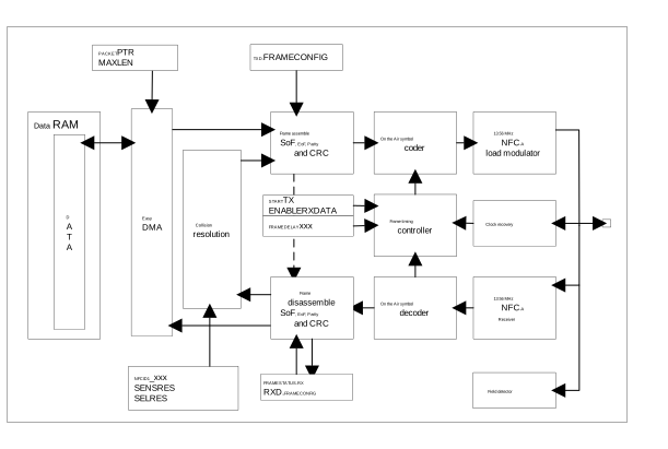
The NFC peripheral contains a 13.56 MHz AM receiver and a 13.56 MHz load modulator compatible with the NFC-A technology defined in the NFC Forum with 106 kbps data rate.
The received frames will be automatically disassembled and the data part of the frame transferred to RAM. When transmitting, the frame data will be transferred directly from RAM and transmitted with configurable frame type and delay timing. The system will be notified by an event whenever a complete frame is received or sent.
It also supports the collision detection and resolution ("anticollision") as defined by the NFC Forum.
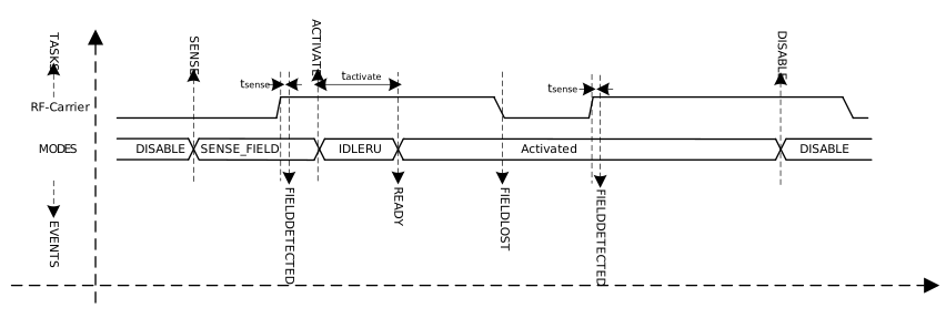
Wake-on-field is supported in SENSE mode while the device is either in System OFF or System ON mode. When the antenna enters an NFC field, an event will be triggered notifying the system to activate the NFC functionality for incoming frames. In System ON, if the energy detected at the antenna increases beyond a threshold value, the module will generate a FIELDDETECTED event. The module will generate a FIELDLOST event when the quality or strength of the field no longer support NFC communication. Please refer to NFCT Electrical Specification for the Low Power Field Detect threshold values.
In system OFF, the NFC Low Power Field Detect function can wake the system up through a reset. The NFC bit in register RESETREAS will be set as cause of the wake-up.
If the system is put into system OFF mode while a field is already present, the NFC Low Power Field Detect function will wake the system up right away and generate a reset.
Note that as a consequence of reset, NFC is disabled, so the reset handler will have to activate NFC again and set it up properly.
The HFXO must be running before the NFC peripheral goes into ACTIVATED state. Note that the NFC peripheral calibration is automatically done on ACTIVATE task. The HFXO can be turned off when the NFC peripheral goes into SENSE mode. The shortcut FIELDDETECTED_ACTIVATE can be used when the HFXO is already running while in SENSE mode.
Outgoing data will be collected from RAM with the EasyDMA function and assembled according to the TXD.FRAMECONFIG register. Incoming data will be disassembled according to the RXD.FRAMECONFIG register and the data section in the frame will be written to RAM via the EasyDMA function.
The NFC peripheral includes a frame timing controller that can be used to accurately control the inter-frame delay between the incoming frame and a corresponding outgoing frame. It also includes optional CRC functionality.
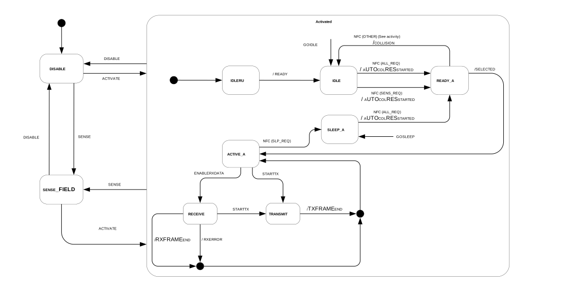
The NFC peripheral has a set of different states. The module can change state by triggering a task, or when specific operations are finalized. Events and tasks allow software to keep track of and change the current state.
See Figure 1 and Figure 2 for more information.
- FIELDLOST event will not be reflected in the state machine (for instance by going back to the DISABLE state), it is up to software to decide on the actions to take when a field lost occurs.
- FIELDLOST event is not generated in SENSE mode.
- FIELDDETECTED event is generated only on the transition from FIELDLOST event to energy detected by the NFC peripheral. So, sending SENSE task while field is still present does not generate FIELDDETECTED event.
- If the FIELDDETECTED event is cleared before sending the ACTIVATE task, then the FIELDDETECTED event shows up again after sending the ACTIVATE task. The shortcut FIELDDETECTED_ACTIVATE can be used to avoid this condition.
Pin configuration
NFC uses two pins to connect the antenna.
These pins are shared with GPIOs, and the PROTECT field in the NFCPINS register in UICR defines the usage of these pins and their protection level against excessive voltages. The content of the NFCPINS register is reloaded at every reset.
When NFCPINS.PROTECT=NFC, a protection circuit will be enabled on the dedicated pins, preventing the chip from being damaged in the presence of a strong NFC field. The GPIO function will be disabled on those pins as well.
When NFCPINS.PROTECT=Disabled, the device will not be protected against strong NFC field damages caught by a connected NFC antenna, and the NFCT peripheral will not operate as expected, as it will never leave the DISABLE state.
The pins dedicated to the NFC antenna function will have some limitation when the pins are configured for normal GPIO operation. The pin capacitance will be higher on those (refer to CPAD_NFC in the GPIO Electrical Specification below), and some increased leakage current between the two pins is to be expected if they are used in GPIO mode, and are driven to different logical values. To save power the two pins should always be set to the same logical value whenever entering one of the device power saving modes. Please refer to INFC_LEAK in GPIO Electrical Specification for details.
EasyDMA
The NFC peripheral implements EasyDMA for reading and writing of data packets from and to the Data RAM without CPU involvement.
The NFC EasyDMA utilizes one pointer called PACKETPTR for receiving and transmitting packets.
The EasyDMA can either read or write between the NFC peripheral and the RAM, but not at the same time. The event RXFRAMESTART indicates that the EasyDMA has started writing to the RAM for a receive frame and the event RXFRAMEND indicates that the EasyDMA has completed writing to the RAM. Similarly, the event TXFRAMESTART indicates that the EasyDMA has started reading from the RAM for a transmit frame and the event TXFRAMEND indicates that the EasyDMA has completed reading from the RAM. If a transmit and a receive operation is issued at the same time, the transmit operation would be prioritized.
Starting a transmit operation while the EasyDMA has already started writing a receive frame to the RAM will result in unpredictable behavior. Starting an EasyDMA operation whilst there is an ongoing EasyDMA operation may result in unpredictable behavior. It is recommended to wait for the TXFRAMEEND or RXFRAMEND event for the respective ongoing transmit or receive before starting a new receive or transmit operation.
The MAXLEN register determines the maximum number of bytes that can be read from or written to the RAM. This feature can be used to secure that the NFC peripheral does not overwrite, or read beyond, the RAM assigned to a packet. Note that if the RXD.AMOUNT or TXD.AMOUNT register indicates longer data packets than set in MAXLEN, the frames sent to or received from the physical layer will be incomplete. In RX, the OVERRUN bit in the FRAMESTATUS.RX register will be set and an RXERROR event will be triggered in that situation.
Note that RXD.AMOUNT and TXD.AMOUNT define a frame length in bytes and bits excluding SoF, EoF and parity, but including CRC for RXD.AMOUNT only, make sure to take potential additional bits into account when setting MAXLEN.
Only sending task ENABLERXDATA ensures that a new value in PACKETPTR pointing to the RX buffer in Data RAM is taken into account.
If PACKETPTR is not pointing to the Data RAM region, an EasyDMA transfer may result in a HardFault or RAM corruption. See Chapter Memory for more information about the different memory regions.
The NFC peripherals normally do alternative receive and transmit frames. So, to prepare for the next frame, the PACKETPTR, MAXLEN, TXD.FRAMECONFIG and TXD.AMOUNT can be updated while the receive is in progress, and, similarly, the PACKETPTR, MAXLEN and RXD.FRAMECONFIG can be updated while the transmit is in progress. They can be updated and prepared for the next NFC frame immediately after the STARTED event of the current frame has been received. Updating the TXD.FRAMECONFIG and TXD.AMOUNT during the current transmit frame or updating RXD.FRAMECONFIG during current receive frame may cause unpredictable behaviour.
In accordance with NFC Forum, NFC Digital Protocol Technical Specification, the least a significant bit from the least significant byte is sent on air first. The bytes are stored in increasing order, starting at the lowest address in the EasyDMA buffer in RAM.
Collision resolution
The NFC peripheral implements an automatic collision resolution function as defined by the NFC Forum.
- NFCID1_LAST if NFCID1SIZE=NFCID1Single (ID = 4 bytes);
- NFCID1_2ND_LAST and NFCID1_LAST if NFCID1SIZE=NFCID1Double (ID = 7 bytes);
- NFCID1_3RD_LAST, NFCID1_2ND_LAST and NFCID1_LAST if NFCID1SIZE=NFCID1Triple (ID = 10 bytes);
| ID = 4 bytes | ID = 7 bytes | ID = 10 bytes | |
|---|---|---|---|
| NFCID1_Q | nfcid10 | ||
| NFCID1_R | nfcid11 | ||
| NFCID1_S | nfcid12 | ||
| NFCID1_T | nfcid10 | nfcid13 | |
| NFCID1_U | nfcid11 | nfcid14 | |
| NFCID1_V | nfcid12 | nfcid15 | |
| NFCID1_W | nfcid10 | nfcid13 | nfcid16 |
| NFCID1_X | nfcid11 | nfcid14 | nfcid17 |
| NFCID1_Y | nfcid12 | nfcid15 | nfcid18 |
| NFCID1_Z | nfcid13 | nfcid16 | nfcid19 |
Automatic collision resolution is enabled by default.
The hardware implementation can handle the states from IDLE to ACTIVE_A automatically as defined in the NFC Forum, NFC Activity Technical Specification, and the other states are to be handled by software. The software keeps track of the state through events. The collision resolution will trigger an AUTOCOLRESSTARTED event when it has started. Reaching the ACTIVE_A state is indicated by the SELECTED event.
If collision resolution fails, a COLLISION event is triggered. Note that errors occurring during automatic collision resolution may also cause ERROR and/or RXERROR events to be generated. Also, other events may get generated. It is recommended that the software ignores any event except COLLISION, SELECTED and FIELDLOST during automatic collision resolution. Software shall also make sure that any unwanted SHORT or PPI shortcut are disabled during automatic collision resolution.
A pre-defined set of registers, NFC.TAGHEADER0..3, containing a valid NFCID1 value, is available in FICR, and can be used by software to populate the NFCID1_3RD_LAST, NFCID1_2ND_LAST and NFCID1_LAST registers. Refer to the release notes of the NFC stack for more details on the format.
The automatic collision resolution will be restarted, if the packets are received with CRC or parity errors while in ACTIVE_A state.
The SLP_REQ is automatically handled by the NFC peripheral. However, this results in an ERROR event (with FRAMEDELAYTIMEOUT cause in ERRORSTATUS) since the SLP_REQ has no response. This error must be ignored until the SELECTED event is triggered and this error should be cleared by the software when the SELECTED event is triggered.
Frame timing controller
The NFC peripheral includes a frame timing controller that continuously keeps track of the number of the 13.56 MHz RF-carrier clock periods since the end of the EoF of the last received frame.
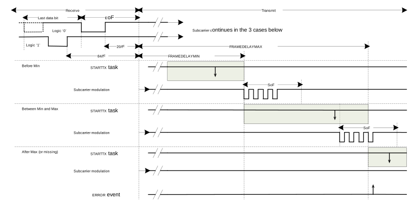
The NFC peripheral can be programmed to send a responding frame within a time window or at an exact count of RF carrier periods. In case of FRAMEDELAYMODE = Window a STARTTX task triggered before the frame timing controller counter is equal to FRAMEDELAYMIN will force the transmission to halt until the counter is equal to FRAMEDELAYMIN. If the counter is within FRAMEDELAYMIN and FRAMEDELAYMAX when the STARTTX task is triggered, the peripheral will start the transmission straight away. In case of FRAMEDELAYMODE = ExactVal, a STARTTX task, triggered before the frame delay counter is equal to FRAMEDELAYMAX, will halt the actual transmission start until the counter is equal to FRAMEDELAYMAX.
In case of FRAMEDELAYMODE = WindowGrid, the behaviour is similar to the FRAMEDELAYMODE = Window, but the actual transmission between FRAMEDELAYMIN and FRAMEDELAYMAX starts on a bit grid as defined for NFC-A Listen frames (slot duration of 128 RF carrier periods).
The FRAMEDELAYMIN and FRAMEDELAYMAX values shall only be updated before the STARTTX task is triggered. Failing to do so may cause unpredictable behaviour. An ERROR event (with FRAMEDELAYTIMEOUT cause in ERRORSTATUS) will be asserted if the frame timing controller counter reaches FRAMEDELAYMAX without any STARTTX task triggered. This may happen even when the response is not required as per NFC Forum, NFC Digital Protocol Technical Specification. Any commands handled by the automatic collision resolution that don't involve a response being generated may also result in an ERROR event (with FRAMEDELAYTIMEOUT cause in ERRORSTATUS).
The frame timing controller operation is illustrated in Figure 3. The frame timing controller automatically adjusts the frame timing counter based on the last received data bit according to NFC-A technology in the NFC Forum, NFC Digital Protocol Technical Specification.
Frame assembler
The NFC peripheral implements a frame assembler in hardware.
When the NFC peripheral is in the ACTIVE_A state, the software can decide to enter RX or TX mode. For RX, see Frame disassembler. For TX, the software must indicate the address of the source buffer in Data RAM and its size through programming the PACKETPTR and MAXCNT registers respectively, then issuing a TXSTART task.
MAXCNT must be set so that it matches the size of the frame to be sent.
The STARTED event indicates that the PACKETPTR and MAXCNT registers have been captured by the frame assembler's EasyDMA.
When asserting the STARTTX task, the frame assembler module will start reading TXD.AMOUNT.TXDATABYTES bytes (plus one additional byte if TXD.AMOUNT.TXDATABITS > 0) from the RAM position set by the PACKETPTR.
The NFC peripheral transmits the data as read from RAM, adding framing and the CRC calculated on the fly. The NFC peripheral will take (8*TXD.AMOUNT.TXDATABYTES + TXD.AMOUNT.TXDATABITS) bits and assemble a frame according to settings in TXD.FRAMECONFIG. Both short frames, standard frames and bit oriented SDD frames as specified in the NFC Forum, NFC Digital Protocol Technical Specification can be assembled by correct setting of the TXD.FRAMECONFIG register.
The bytes will be transmitted on air in the same order as they are read from RAM with a rising bit order within each byte (least significant bit first). That is, b0 will be transmitted on air before b1, and so on. The bits read from RAM will be coded into symbols as defined in the NFC Forum, NFC Digital Protocol Technical Specification.
The frame assembler can be configured in TXD.FRAMECONFIG to add Start of Frame (SoF) symbol, calculate and add parity bits, and calculate and add CRC to the data read from RAM when assembling the frame. The total frame will then be longer than what is defined by TXD.AMOUNT.TXDATABYTES and TXDATABITS. DISCARDMODE will select if the first bits in the first byte read from RAM or the last bits in the last byte read from RAM will be discarded if TXD.AMOUNT.TXDATABITS are not equal to zero. Note that if TXD.FRAMECONFIG.PARITY = Parity and TXD.FRAMECONFIG.DISCARDMODE=DiscardStart, a parity bit will be included after the non-complete first byte. No parity will be added after a non-complete last byte.
The Frame Assemble operation is illustrated in Figure 4 for different settings in TXD.FRAMECONFIG. All shaded bits fields are added by the frame assembler. Some of these bits are optional and appearances are configured in TXD.FRAMECONFIG. Please note that the frames illustrated do not necessarily comply with the NFC specification. The figure is only to illustrate the behavior of the NFC peripheral.
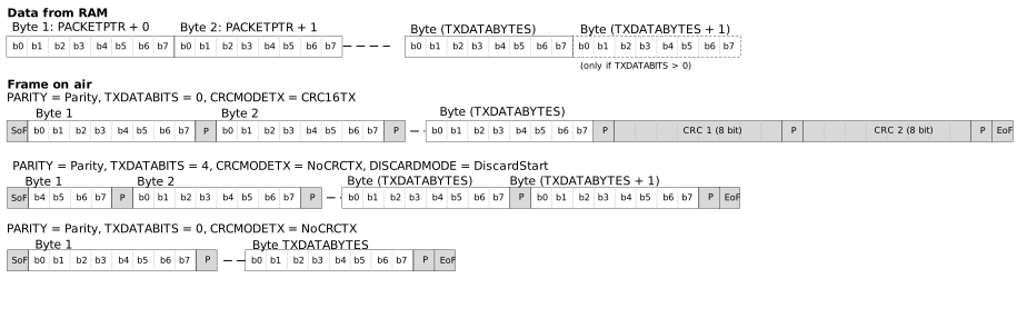
The accurate timing for transmitting the frame on air is set using the frame timing controller settings.
Frame disassembler
The NFC peripheral implements a frame disassembler in hardware.
When the NFC peripheral is in the ACTIVE_A state, the software can decide to enter RX or TX mode. For TX, see Frame assembler. For RX, the software must indicate the address of the destination buffer in Data RAM and its size through programming the PACKETPTR and MAXCNT registers respectively, then issuing a ENABLERXDATA task.
The STARTED event indicates that the PACKETPTR and MAXCNT registers have been captured by the frame disassembler's EasyDMA.
When an incoming frame starts, the RXFRAMESTART event will get issued and data will be written to the buffer in Data RAM. The frame disassembler will verify and remove on the fly any parity bits and SoF and End of Frame (EoF) symbols based on RXD.FRAMECONFIG register configuration. It will, however, verify and transfer the CRC bytes into RAM, if the CRC is was enabled through RXD.FRAMECONFIG.
When an EoF symbol is detected, the NFC peripheral will assert the RXFRAMEEND event and write the RXD.AMOUNT register to indicate numbers of received bytes and bits in the data packet. The module does not interpret the content of the data received from the remote NFC device, except for SoF, EoF, parity and CRC checking, as described above. The Frame disassemble operation is illustrated in Figure 5.
Per NFC specification, the time between end of frame to the next start of frame can be as short as 86 μs, so care must be taken that PACKETPTR and MAXCNT are ready and ENABLERXDATA is issued on time after the end of previous frame. The use of a PPI shortcut from TXFRAMEEND to ENABLERXDATA is recommended.
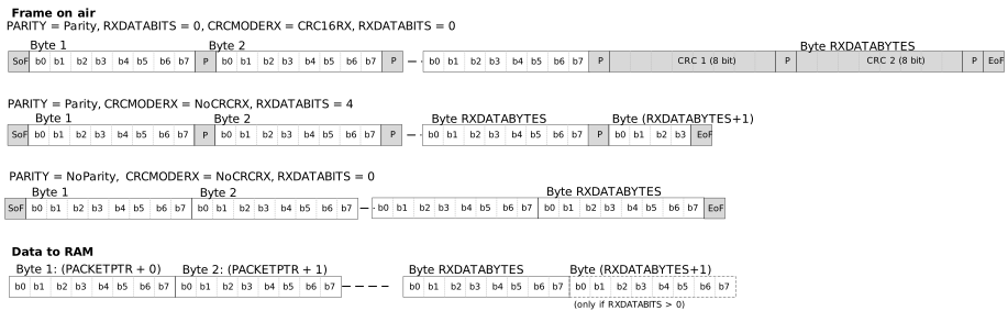
Antenna interface
In ACTIVATED state, an amplitude regulator will adjust the voltage swing on the antenna pins to a value that is within the Vswing limit.
Refer to NFCT Electrical Specification.
NFCT antenna recommendations
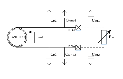
The NFCT antenna coil must be connected differential between NFC1 and NFC2 pins of the device.
Two external capacitors should be used to tune the resonance of the antenna circuit to 13.56 MHz.
The required tuning capacitor value is given by the below equations:
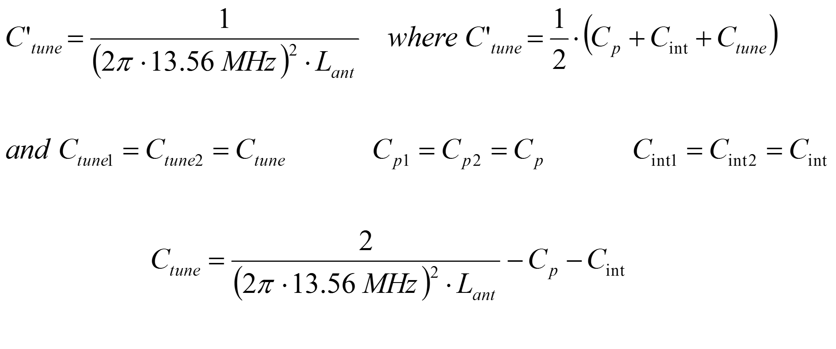
An antenna inductance of Lant = 2 μH will give tuning capacitors in the range of 130 pF on each pin. For good performance, match the total capacitance on NFC1 and NFC2.
Battery protection
If the antenna is exposed to a strong NFC field, current may flow in the opposite direction on the supply due to parasitic diodes and ESD structures.
If the battery used does not tolerate return current, a series diode must be placed between the battery and the device in order to protect the battery.
References
NFC Forum, NFC Analog Specification version 1.0, www.nfc-forum.org
NFC Forum, NFC Digital Protocol Technical Specification version 1.1, www.nfc-forum.org
NFC Forum, NFC Activity Technical Specification version 1.1, www.nfc-forum.org
Registers
| Base address | Peripheral | Instance | Description | Configuration | |
|---|---|---|---|---|---|
| 0x40005000 | NFCT | NFCT | Near Field Communication Tag | ||
| Register | Offset | Description | |
|---|---|---|---|
| TASKS_ACTIVATE | 0x000 | Activate NFC peripheral for incoming and outgoing frames, change state to activated | |
| TASKS_DISABLE | 0x004 | Disable NFC peripheral | |
| TASKS_SENSE | 0x008 | Enable NFC sense field mode, change state to sense mode | |
| TASKS_STARTTX | 0x00C | Start transmission of a outgoing frame, change state to transmit | |
| TASKS_ENABLERXDATA | 0x01C | Initializes the EasyDMA for receive. | |
| TASKS_GOIDLE | 0x024 | Force state machine to IDLE state | |
| TASKS_GOSLEEP | 0x028 | Force state machine to SLEEP_A state | |
| EVENTS_READY | 0x100 | The NFC peripheral is ready to receive and send frames | |
| EVENTS_FIELDDETECTED | 0x104 | Remote NFC field detected | |
| EVENTS_FIELDLOST | 0x108 | Remote NFC field lost | |
| EVENTS_TXFRAMESTART | 0x10C | Marks the start of the first symbol of a transmitted frame | |
| EVENTS_TXFRAMEEND | 0x110 | Marks the end of the last transmitted on-air symbol of a frame | |
| EVENTS_RXFRAMESTART | 0x114 | Marks the end of the first symbol of a received frame | |
| EVENTS_RXFRAMEEND | 0x118 | Received data have been checked (CRC, parity) and transferred to RAM, and EasyDMA has ended accessing the RX buffer | |
| EVENTS_ERROR | 0x11C | NFC error reported. The ERRORSTATUS register contains details on the source of the error. | |
| EVENTS_RXERROR | 0x128 | NFC RX frame error reported. The FRAMESTATUS.RX register contains details on the source of the error. | |
| EVENTS_ENDRX | 0x12C | RX buffer (as defined by PACKETPTR and MAXLEN) in Data RAM full. | |
| EVENTS_ENDTX | 0x130 | Transmission of data in RAM has ended, and EasyDMA has ended accessing the TX buffer | |
| EVENTS_AUTOCOLRESSTARTED | 0x138 | Auto collision resolution process has started | |
| EVENTS_COLLISION | 0x148 | NFC Auto collision resolution error reported. | |
| EVENTS_SELECTED | 0x14C | NFC Auto collision resolution successfully completed | |
| EVENTS_STARTED | 0x150 | EasyDMA is ready to receive or send frames. | |
| SHORTS | 0x200 | Shortcut register | |
| INTEN | 0x300 | Enable or disable interrupt | |
| INTENSET | 0x304 | Enable interrupt | |
| INTENCLR | 0x308 | Disable interrupt | |
| ERRORSTATUS | 0x404 | NFC Error Status register | |
| FRAMESTATUS.RX | 0x40C | Result of last incoming frames | |
| CURRENTLOADCTRL | 0x430 | Current value driven to the NFC Load Control | |
| FIELDPRESENT | 0x43C | Indicates the presence or not of a valid field | |
| FRAMEDELAYMIN | 0x504 | Minimum frame delay | |
| FRAMEDELAYMAX | 0x508 | Maximum frame delay | |
| FRAMEDELAYMODE | 0x50C | Configuration register for the Frame Delay Timer | |
| PACKETPTR | 0x510 | Packet pointer for TXD and RXD data storage in Data RAM | |
| MAXLEN | 0x514 | Size of allocated for TXD and RXD data storage buffer in Data RAM | |
| TXD.FRAMECONFIG | 0x518 | Configuration of outgoing frames | |
| TXD.AMOUNT | 0x51C | Size of outgoing frame | |
| RXD.FRAMECONFIG | 0x520 | Configuration of incoming frames | |
| RXD.AMOUNT | 0x524 | Size of last incoming frame | |
| NFCID1_LAST | 0x590 | Last NFCID1 part (4, 7 or 10 bytes ID) | |
| NFCID1_2ND_LAST | 0x594 | Second last NFCID1 part (7 or 10 bytes ID) | |
| NFCID1_3RD_LAST | 0x598 | Third last NFCID1 part (10 bytes ID) | |
| SENSRES | 0x5A0 | NFC-A SENS_RES auto-response settings | |
| SELRES | 0x5A4 | NFC-A SEL_RES auto-response settings | |
SHORTS
Address offset: 0x200
Shortcut register
| Bit number | 31 | 30 | 29 | 28 | 27 | 26 | 25 | 24 | 23 | 22 | 21 | 20 | 19 | 18 | 17 | 16 | 15 | 14 | 13 | 12 | 11 | 10 | 9 | 8 | 7 | 6 | 5 | 4 | 3 | 2 | 1 | 0 | |||
|---|---|---|---|---|---|---|---|---|---|---|---|---|---|---|---|---|---|---|---|---|---|---|---|---|---|---|---|---|---|---|---|---|---|---|---|
| Id | B | A | |||||||||||||||||||||||||||||||||
| Reset 0x00000000 | 0 | 0 | 0 | 0 | 0 | 0 | 0 | 0 | 0 | 0 | 0 | 0 | 0 | 0 | 0 | 0 | 0 | 0 | 0 | 0 | 0 | 0 | 0 | 0 | 0 | 0 | 0 | 0 | 0 | 0 | 0 | 0 | |||
| Id | RW | Field | Value Id | Value | Description | ||||||||||||||||||||||||||||||
| A | RW | FIELDDETECTED_ACTIVATE | Shortcut between FIELDDETECTED event and ACTIVATE task See EVENTS_FIELDDETECTED and TASKS_ACTIVATE | ||||||||||||||||||||||||||||||||
Disabled | 0 | Disable shortcut | |||||||||||||||||||||||||||||||||
Enabled | 1 | Enable shortcut | |||||||||||||||||||||||||||||||||
| B | RW | FIELDLOST_SENSE | Shortcut between FIELDLOST event and SENSE task See EVENTS_FIELDLOST and TASKS_SENSE | ||||||||||||||||||||||||||||||||
Disabled | 0 | Disable shortcut | |||||||||||||||||||||||||||||||||
Enabled | 1 | Enable shortcut | |||||||||||||||||||||||||||||||||
INTEN
Address offset: 0x300
Enable or disable interrupt
| Bit number | 31 | 30 | 29 | 28 | 27 | 26 | 25 | 24 | 23 | 22 | 21 | 20 | 19 | 18 | 17 | 16 | 15 | 14 | 13 | 12 | 11 | 10 | 9 | 8 | 7 | 6 | 5 | 4 | 3 | 2 | 1 | 0 | |||
|---|---|---|---|---|---|---|---|---|---|---|---|---|---|---|---|---|---|---|---|---|---|---|---|---|---|---|---|---|---|---|---|---|---|---|---|
| Id | T | S | R | N | M | L | K | H | G | F | E | D | C | B | A | ||||||||||||||||||||
| Reset 0x00000000 | 0 | 0 | 0 | 0 | 0 | 0 | 0 | 0 | 0 | 0 | 0 | 0 | 0 | 0 | 0 | 0 | 0 | 0 | 0 | 0 | 0 | 0 | 0 | 0 | 0 | 0 | 0 | 0 | 0 | 0 | 0 | 0 | |||
| Id | RW | Field | Value Id | Value | Description | ||||||||||||||||||||||||||||||
| A | RW | READY | Enable or disable interrupt for READY event See EVENTS_READY | ||||||||||||||||||||||||||||||||
Disabled | 0 | Disable | |||||||||||||||||||||||||||||||||
Enabled | 1 | Enable | |||||||||||||||||||||||||||||||||
| B | RW | FIELDDETECTED | Enable or disable interrupt for FIELDDETECTED event | ||||||||||||||||||||||||||||||||
Disabled | 0 | Disable | |||||||||||||||||||||||||||||||||
Enabled | 1 | Enable | |||||||||||||||||||||||||||||||||
| C | RW | FIELDLOST | Enable or disable interrupt for FIELDLOST event See EVENTS_FIELDLOST | ||||||||||||||||||||||||||||||||
Disabled | 0 | Disable | |||||||||||||||||||||||||||||||||
Enabled | 1 | Enable | |||||||||||||||||||||||||||||||||
| D | RW | TXFRAMESTART | Enable or disable interrupt for TXFRAMESTART event | ||||||||||||||||||||||||||||||||
Disabled | 0 | Disable | |||||||||||||||||||||||||||||||||
Enabled | 1 | Enable | |||||||||||||||||||||||||||||||||
| E | RW | TXFRAMEEND | Enable or disable interrupt for TXFRAMEEND event | ||||||||||||||||||||||||||||||||
Disabled | 0 | Disable | |||||||||||||||||||||||||||||||||
Enabled | 1 | Enable | |||||||||||||||||||||||||||||||||
| F | RW | RXFRAMESTART | Enable or disable interrupt for RXFRAMESTART event | ||||||||||||||||||||||||||||||||
Disabled | 0 | Disable | |||||||||||||||||||||||||||||||||
Enabled | 1 | Enable | |||||||||||||||||||||||||||||||||
| G | RW | RXFRAMEEND | Enable or disable interrupt for RXFRAMEEND event | ||||||||||||||||||||||||||||||||
Disabled | 0 | Disable | |||||||||||||||||||||||||||||||||
Enabled | 1 | Enable | |||||||||||||||||||||||||||||||||
| H | RW | ERROR | Enable or disable interrupt for ERROR event See EVENTS_ERROR | ||||||||||||||||||||||||||||||||
Disabled | 0 | Disable | |||||||||||||||||||||||||||||||||
Enabled | 1 | Enable | |||||||||||||||||||||||||||||||||
| K | RW | RXERROR | Enable or disable interrupt for RXERROR event See EVENTS_RXERROR | ||||||||||||||||||||||||||||||||
Disabled | 0 | Disable | |||||||||||||||||||||||||||||||||
Enabled | 1 | Enable | |||||||||||||||||||||||||||||||||
| L | RW | ENDRX | Enable or disable interrupt for ENDRX event See EVENTS_ENDRX | ||||||||||||||||||||||||||||||||
Disabled | 0 | Disable | |||||||||||||||||||||||||||||||||
Enabled | 1 | Enable | |||||||||||||||||||||||||||||||||
| M | RW | ENDTX | Enable or disable interrupt for ENDTX event See EVENTS_ENDTX | ||||||||||||||||||||||||||||||||
Disabled | 0 | Disable | |||||||||||||||||||||||||||||||||
Enabled | 1 | Enable | |||||||||||||||||||||||||||||||||
| N | RW | AUTOCOLRESSTARTED | Enable or disable interrupt for AUTOCOLRESSTARTED event | ||||||||||||||||||||||||||||||||
Disabled | 0 | Disable | |||||||||||||||||||||||||||||||||
Enabled | 1 | Enable | |||||||||||||||||||||||||||||||||
| R | RW | COLLISION | Enable or disable interrupt for COLLISION event See EVENTS_COLLISION | ||||||||||||||||||||||||||||||||
Disabled | 0 | Disable | |||||||||||||||||||||||||||||||||
Enabled | 1 | Enable | |||||||||||||||||||||||||||||||||
| S | RW | SELECTED | Enable or disable interrupt for SELECTED event See EVENTS_SELECTED | ||||||||||||||||||||||||||||||||
Disabled | 0 | Disable | |||||||||||||||||||||||||||||||||
Enabled | 1 | Enable | |||||||||||||||||||||||||||||||||
| T | RW | STARTED | Enable or disable interrupt for STARTED event See EVENTS_STARTED | ||||||||||||||||||||||||||||||||
Disabled | 0 | Disable | |||||||||||||||||||||||||||||||||
Enabled | 1 | Enable | |||||||||||||||||||||||||||||||||
INTENSET
Address offset: 0x304
Enable interrupt
| Bit number | 31 | 30 | 29 | 28 | 27 | 26 | 25 | 24 | 23 | 22 | 21 | 20 | 19 | 18 | 17 | 16 | 15 | 14 | 13 | 12 | 11 | 10 | 9 | 8 | 7 | 6 | 5 | 4 | 3 | 2 | 1 | 0 | |||
|---|---|---|---|---|---|---|---|---|---|---|---|---|---|---|---|---|---|---|---|---|---|---|---|---|---|---|---|---|---|---|---|---|---|---|---|
| Id | T | S | R | N | M | L | K | H | G | F | E | D | C | B | A | ||||||||||||||||||||
| Reset 0x00000000 | 0 | 0 | 0 | 0 | 0 | 0 | 0 | 0 | 0 | 0 | 0 | 0 | 0 | 0 | 0 | 0 | 0 | 0 | 0 | 0 | 0 | 0 | 0 | 0 | 0 | 0 | 0 | 0 | 0 | 0 | 0 | 0 | |||
| Id | RW | Field | Value Id | Value | Description | ||||||||||||||||||||||||||||||
| A | RW | READY | Write '1' to Enable interrupt for READY event See EVENTS_READY | ||||||||||||||||||||||||||||||||
Set | 1 | Enable | |||||||||||||||||||||||||||||||||
Disabled | 0 | Read: Disabled | |||||||||||||||||||||||||||||||||
Enabled | 1 | Read: Enabled | |||||||||||||||||||||||||||||||||
| B | RW | FIELDDETECTED | Write '1' to Enable interrupt for FIELDDETECTED event | ||||||||||||||||||||||||||||||||
Set | 1 | Enable | |||||||||||||||||||||||||||||||||
Disabled | 0 | Read: Disabled | |||||||||||||||||||||||||||||||||
Enabled | 1 | Read: Enabled | |||||||||||||||||||||||||||||||||
| C | RW | FIELDLOST | Write '1' to Enable interrupt for FIELDLOST event See EVENTS_FIELDLOST | ||||||||||||||||||||||||||||||||
Set | 1 | Enable | |||||||||||||||||||||||||||||||||
Disabled | 0 | Read: Disabled | |||||||||||||||||||||||||||||||||
Enabled | 1 | Read: Enabled | |||||||||||||||||||||||||||||||||
| D | RW | TXFRAMESTART | Write '1' to Enable interrupt for TXFRAMESTART event | ||||||||||||||||||||||||||||||||
Set | 1 | Enable | |||||||||||||||||||||||||||||||||
Disabled | 0 | Read: Disabled | |||||||||||||||||||||||||||||||||
Enabled | 1 | Read: Enabled | |||||||||||||||||||||||||||||||||
| E | RW | TXFRAMEEND | Write '1' to Enable interrupt for TXFRAMEEND event | ||||||||||||||||||||||||||||||||
Set | 1 | Enable | |||||||||||||||||||||||||||||||||
Disabled | 0 | Read: Disabled | |||||||||||||||||||||||||||||||||
Enabled | 1 | Read: Enabled | |||||||||||||||||||||||||||||||||
| F | RW | RXFRAMESTART | Write '1' to Enable interrupt for RXFRAMESTART event | ||||||||||||||||||||||||||||||||
Set | 1 | Enable | |||||||||||||||||||||||||||||||||
Disabled | 0 | Read: Disabled | |||||||||||||||||||||||||||||||||
Enabled | 1 | Read: Enabled | |||||||||||||||||||||||||||||||||
| G | RW | RXFRAMEEND | Write '1' to Enable interrupt for RXFRAMEEND event | ||||||||||||||||||||||||||||||||
Set | 1 | Enable | |||||||||||||||||||||||||||||||||
Disabled | 0 | Read: Disabled | |||||||||||||||||||||||||||||||||
Enabled | 1 | Read: Enabled | |||||||||||||||||||||||||||||||||
| H | RW | ERROR | Write '1' to Enable interrupt for ERROR event See EVENTS_ERROR | ||||||||||||||||||||||||||||||||
Set | 1 | Enable | |||||||||||||||||||||||||||||||||
Disabled | 0 | Read: Disabled | |||||||||||||||||||||||||||||||||
Enabled | 1 | Read: Enabled | |||||||||||||||||||||||||||||||||
| K | RW | RXERROR | Write '1' to Enable interrupt for RXERROR event See EVENTS_RXERROR | ||||||||||||||||||||||||||||||||
Set | 1 | Enable | |||||||||||||||||||||||||||||||||
Disabled | 0 | Read: Disabled | |||||||||||||||||||||||||||||||||
Enabled | 1 | Read: Enabled | |||||||||||||||||||||||||||||||||
| L | RW | ENDRX | Write '1' to Enable interrupt for ENDRX event See EVENTS_ENDRX | ||||||||||||||||||||||||||||||||
Set | 1 | Enable | |||||||||||||||||||||||||||||||||
Disabled | 0 | Read: Disabled | |||||||||||||||||||||||||||||||||
Enabled | 1 | Read: Enabled | |||||||||||||||||||||||||||||||||
| M | RW | ENDTX | Write '1' to Enable interrupt for ENDTX event See EVENTS_ENDTX | ||||||||||||||||||||||||||||||||
Set | 1 | Enable | |||||||||||||||||||||||||||||||||
Disabled | 0 | Read: Disabled | |||||||||||||||||||||||||||||||||
Enabled | 1 | Read: Enabled | |||||||||||||||||||||||||||||||||
| N | RW | AUTOCOLRESSTARTED | Write '1' to Enable interrupt for AUTOCOLRESSTARTED event | ||||||||||||||||||||||||||||||||
Set | 1 | Enable | |||||||||||||||||||||||||||||||||
Disabled | 0 | Read: Disabled | |||||||||||||||||||||||||||||||||
Enabled | 1 | Read: Enabled | |||||||||||||||||||||||||||||||||
| R | RW | COLLISION | Write '1' to Enable interrupt for COLLISION event See EVENTS_COLLISION | ||||||||||||||||||||||||||||||||
Set | 1 | Enable | |||||||||||||||||||||||||||||||||
Disabled | 0 | Read: Disabled | |||||||||||||||||||||||||||||||||
Enabled | 1 | Read: Enabled | |||||||||||||||||||||||||||||||||
| S | RW | SELECTED | Write '1' to Enable interrupt for SELECTED event See EVENTS_SELECTED | ||||||||||||||||||||||||||||||||
Set | 1 | Enable | |||||||||||||||||||||||||||||||||
Disabled | 0 | Read: Disabled | |||||||||||||||||||||||||||||||||
Enabled | 1 | Read: Enabled | |||||||||||||||||||||||||||||||||
| T | RW | STARTED | Write '1' to Enable interrupt for STARTED event See EVENTS_STARTED | ||||||||||||||||||||||||||||||||
Set | 1 | Enable | |||||||||||||||||||||||||||||||||
Disabled | 0 | Read: Disabled | |||||||||||||||||||||||||||||||||
Enabled | 1 | Read: Enabled | |||||||||||||||||||||||||||||||||
INTENCLR
Address offset: 0x308
Disable interrupt
| Bit number | 31 | 30 | 29 | 28 | 27 | 26 | 25 | 24 | 23 | 22 | 21 | 20 | 19 | 18 | 17 | 16 | 15 | 14 | 13 | 12 | 11 | 10 | 9 | 8 | 7 | 6 | 5 | 4 | 3 | 2 | 1 | 0 | |||
|---|---|---|---|---|---|---|---|---|---|---|---|---|---|---|---|---|---|---|---|---|---|---|---|---|---|---|---|---|---|---|---|---|---|---|---|
| Id | T | S | R | N | M | L | K | H | G | F | E | D | C | B | A | ||||||||||||||||||||
| Reset 0x00000000 | 0 | 0 | 0 | 0 | 0 | 0 | 0 | 0 | 0 | 0 | 0 | 0 | 0 | 0 | 0 | 0 | 0 | 0 | 0 | 0 | 0 | 0 | 0 | 0 | 0 | 0 | 0 | 0 | 0 | 0 | 0 | 0 | |||
| Id | RW | Field | Value Id | Value | Description | ||||||||||||||||||||||||||||||
| A | RW | READY | Write '1' to Disable interrupt for READY event See EVENTS_READY | ||||||||||||||||||||||||||||||||
Clear | 1 | Disable | |||||||||||||||||||||||||||||||||
Disabled | 0 | Read: Disabled | |||||||||||||||||||||||||||||||||
Enabled | 1 | Read: Enabled | |||||||||||||||||||||||||||||||||
| B | RW | FIELDDETECTED | Write '1' to Disable interrupt for FIELDDETECTED event | ||||||||||||||||||||||||||||||||
Clear | 1 | Disable | |||||||||||||||||||||||||||||||||
Disabled | 0 | Read: Disabled | |||||||||||||||||||||||||||||||||
Enabled | 1 | Read: Enabled | |||||||||||||||||||||||||||||||||
| C | RW | FIELDLOST | Write '1' to Disable interrupt for FIELDLOST event See EVENTS_FIELDLOST | ||||||||||||||||||||||||||||||||
Clear | 1 | Disable | |||||||||||||||||||||||||||||||||
Disabled | 0 | Read: Disabled | |||||||||||||||||||||||||||||||||
Enabled | 1 | Read: Enabled | |||||||||||||||||||||||||||||||||
| D | RW | TXFRAMESTART | Write '1' to Disable interrupt for TXFRAMESTART event | ||||||||||||||||||||||||||||||||
Clear | 1 | Disable | |||||||||||||||||||||||||||||||||
Disabled | 0 | Read: Disabled | |||||||||||||||||||||||||||||||||
Enabled | 1 | Read: Enabled | |||||||||||||||||||||||||||||||||
| E | RW | TXFRAMEEND | Write '1' to Disable interrupt for TXFRAMEEND event | ||||||||||||||||||||||||||||||||
Clear | 1 | Disable | |||||||||||||||||||||||||||||||||
Disabled | 0 | Read: Disabled | |||||||||||||||||||||||||||||||||
Enabled | 1 | Read: Enabled | |||||||||||||||||||||||||||||||||
| F | RW | RXFRAMESTART | Write '1' to Disable interrupt for RXFRAMESTART event | ||||||||||||||||||||||||||||||||
Clear | 1 | Disable | |||||||||||||||||||||||||||||||||
Disabled | 0 | Read: Disabled | |||||||||||||||||||||||||||||||||
Enabled | 1 | Read: Enabled | |||||||||||||||||||||||||||||||||
| G | RW | RXFRAMEEND | Write '1' to Disable interrupt for RXFRAMEEND event | ||||||||||||||||||||||||||||||||
Clear | 1 | Disable | |||||||||||||||||||||||||||||||||
Disabled | 0 | Read: Disabled | |||||||||||||||||||||||||||||||||
Enabled | 1 | Read: Enabled | |||||||||||||||||||||||||||||||||
| H | RW | ERROR | Write '1' to Disable interrupt for ERROR event See EVENTS_ERROR | ||||||||||||||||||||||||||||||||
Clear | 1 | Disable | |||||||||||||||||||||||||||||||||
Disabled | 0 | Read: Disabled | |||||||||||||||||||||||||||||||||
Enabled | 1 | Read: Enabled | |||||||||||||||||||||||||||||||||
| K | RW | RXERROR | Write '1' to Disable interrupt for RXERROR event See EVENTS_RXERROR | ||||||||||||||||||||||||||||||||
Clear | 1 | Disable | |||||||||||||||||||||||||||||||||
Disabled | 0 | Read: Disabled | |||||||||||||||||||||||||||||||||
Enabled | 1 | Read: Enabled | |||||||||||||||||||||||||||||||||
| L | RW | ENDRX | Write '1' to Disable interrupt for ENDRX event See EVENTS_ENDRX | ||||||||||||||||||||||||||||||||
Clear | 1 | Disable | |||||||||||||||||||||||||||||||||
Disabled | 0 | Read: Disabled | |||||||||||||||||||||||||||||||||
Enabled | 1 | Read: Enabled | |||||||||||||||||||||||||||||||||
| M | RW | ENDTX | Write '1' to Disable interrupt for ENDTX event See EVENTS_ENDTX | ||||||||||||||||||||||||||||||||
Clear | 1 | Disable | |||||||||||||||||||||||||||||||||
Disabled | 0 | Read: Disabled | |||||||||||||||||||||||||||||||||
Enabled | 1 | Read: Enabled | |||||||||||||||||||||||||||||||||
| N | RW | AUTOCOLRESSTARTED | Write '1' to Disable interrupt for AUTOCOLRESSTARTED event | ||||||||||||||||||||||||||||||||
Clear | 1 | Disable | |||||||||||||||||||||||||||||||||
Disabled | 0 | Read: Disabled | |||||||||||||||||||||||||||||||||
Enabled | 1 | Read: Enabled | |||||||||||||||||||||||||||||||||
| R | RW | COLLISION | Write '1' to Disable interrupt for COLLISION event See EVENTS_COLLISION | ||||||||||||||||||||||||||||||||
Clear | 1 | Disable | |||||||||||||||||||||||||||||||||
Disabled | 0 | Read: Disabled | |||||||||||||||||||||||||||||||||
Enabled | 1 | Read: Enabled | |||||||||||||||||||||||||||||||||
| S | RW | SELECTED | Write '1' to Disable interrupt for SELECTED event See EVENTS_SELECTED | ||||||||||||||||||||||||||||||||
Clear | 1 | Disable | |||||||||||||||||||||||||||||||||
Disabled | 0 | Read: Disabled | |||||||||||||||||||||||||||||||||
Enabled | 1 | Read: Enabled | |||||||||||||||||||||||||||||||||
| T | RW | STARTED | Write '1' to Disable interrupt for STARTED event See EVENTS_STARTED | ||||||||||||||||||||||||||||||||
Clear | 1 | Disable | |||||||||||||||||||||||||||||||||
Disabled | 0 | Read: Disabled | |||||||||||||||||||||||||||||||||
Enabled | 1 | Read: Enabled | |||||||||||||||||||||||||||||||||
ERRORSTATUS
Address offset: 0x404
NFC Error Status register
Write a bit to '1' to clear it. Writing '0' has no effect.
| Bit number | 31 | 30 | 29 | 28 | 27 | 26 | 25 | 24 | 23 | 22 | 21 | 20 | 19 | 18 | 17 | 16 | 15 | 14 | 13 | 12 | 11 | 10 | 9 | 8 | 7 | 6 | 5 | 4 | 3 | 2 | 1 | 0 | |||
|---|---|---|---|---|---|---|---|---|---|---|---|---|---|---|---|---|---|---|---|---|---|---|---|---|---|---|---|---|---|---|---|---|---|---|---|
| Id | D | C | A | ||||||||||||||||||||||||||||||||
| Reset 0x00000000 | 0 | 0 | 0 | 0 | 0 | 0 | 0 | 0 | 0 | 0 | 0 | 0 | 0 | 0 | 0 | 0 | 0 | 0 | 0 | 0 | 0 | 0 | 0 | 0 | 0 | 0 | 0 | 0 | 0 | 0 | 0 | 0 | |||
| Id | RW | Field | Value Id | Value | Description | ||||||||||||||||||||||||||||||
| A | RW | FRAMEDELAYTIMEOUT | No STARTTX task triggered before expiration of the time set in FRAMEDELAYMAX | ||||||||||||||||||||||||||||||||
| C | RW | NFCFIELDTOOSTRONG | Field level is too high at max load resistance | ||||||||||||||||||||||||||||||||
| D | RW | NFCFIELDTOOWEAK | Field level is too low at min load resistance | ||||||||||||||||||||||||||||||||
FRAMESTATUS.RX
Address offset: 0x40C
Result of last incoming frames
Write a bit to '1' to clear it. Writing '0' has no effect.
| Bit number | 31 | 30 | 29 | 28 | 27 | 26 | 25 | 24 | 23 | 22 | 21 | 20 | 19 | 18 | 17 | 16 | 15 | 14 | 13 | 12 | 11 | 10 | 9 | 8 | 7 | 6 | 5 | 4 | 3 | 2 | 1 | 0 | |||
|---|---|---|---|---|---|---|---|---|---|---|---|---|---|---|---|---|---|---|---|---|---|---|---|---|---|---|---|---|---|---|---|---|---|---|---|
| Id | C | B | A | ||||||||||||||||||||||||||||||||
| Reset 0x00000000 | 0 | 0 | 0 | 0 | 0 | 0 | 0 | 0 | 0 | 0 | 0 | 0 | 0 | 0 | 0 | 0 | 0 | 0 | 0 | 0 | 0 | 0 | 0 | 0 | 0 | 0 | 0 | 0 | 0 | 0 | 0 | 0 | |||
| Id | RW | Field | Value Id | Value | Description | ||||||||||||||||||||||||||||||
| A | RW | CRCERROR | No valid End of Frame detected | ||||||||||||||||||||||||||||||||
CRCCorrect | 0 | Valid CRC detected | |||||||||||||||||||||||||||||||||
CRCError | 1 | CRC received does not match local check | |||||||||||||||||||||||||||||||||
| B | RW | PARITYSTATUS | Parity status of received frame | ||||||||||||||||||||||||||||||||
ParityOK | 0 | Frame received with parity OK | |||||||||||||||||||||||||||||||||
ParityError | 1 | Frame received with parity error | |||||||||||||||||||||||||||||||||
| C | RW | OVERRUN | Overrun detected | ||||||||||||||||||||||||||||||||
NoOverrun | 0 | No overrun detected | |||||||||||||||||||||||||||||||||
Overrun | 1 | Overrun error | |||||||||||||||||||||||||||||||||
CURRENTLOADCTRL
Address offset: 0x430
Current value driven to the NFC Load Control
| Bit number | 31 | 30 | 29 | 28 | 27 | 26 | 25 | 24 | 23 | 22 | 21 | 20 | 19 | 18 | 17 | 16 | 15 | 14 | 13 | 12 | 11 | 10 | 9 | 8 | 7 | 6 | 5 | 4 | 3 | 2 | 1 | 0 | |||
|---|---|---|---|---|---|---|---|---|---|---|---|---|---|---|---|---|---|---|---|---|---|---|---|---|---|---|---|---|---|---|---|---|---|---|---|
| Id | A | A | A | A | A | A | |||||||||||||||||||||||||||||
| Reset 0x00000000 | 0 | 0 | 0 | 0 | 0 | 0 | 0 | 0 | 0 | 0 | 0 | 0 | 0 | 0 | 0 | 0 | 0 | 0 | 0 | 0 | 0 | 0 | 0 | 0 | 0 | 0 | 0 | 0 | 0 | 0 | 0 | 0 | |||
| Id | RW | Field | Value Id | Value | Description | ||||||||||||||||||||||||||||||
| A | R | CURRENTLOADCTRL | Current value driven to the NFC Load Control | ||||||||||||||||||||||||||||||||
FIELDPRESENT
Address offset: 0x43C
Indicates the presence or not of a valid field
| Bit number | 31 | 30 | 29 | 28 | 27 | 26 | 25 | 24 | 23 | 22 | 21 | 20 | 19 | 18 | 17 | 16 | 15 | 14 | 13 | 12 | 11 | 10 | 9 | 8 | 7 | 6 | 5 | 4 | 3 | 2 | 1 | 0 | |||
|---|---|---|---|---|---|---|---|---|---|---|---|---|---|---|---|---|---|---|---|---|---|---|---|---|---|---|---|---|---|---|---|---|---|---|---|
| Id | B | A | |||||||||||||||||||||||||||||||||
| Reset 0x00000000 | 0 | 0 | 0 | 0 | 0 | 0 | 0 | 0 | 0 | 0 | 0 | 0 | 0 | 0 | 0 | 0 | 0 | 0 | 0 | 0 | 0 | 0 | 0 | 0 | 0 | 0 | 0 | 0 | 0 | 0 | 0 | 0 | |||
| Id | RW | Field | Value Id | Value | Description | ||||||||||||||||||||||||||||||
| A | R | FIELDPRESENT | Indicates the presence or not of a valid field. Available only in the activated state. | ||||||||||||||||||||||||||||||||
NoField | 0 | No valid field detected | |||||||||||||||||||||||||||||||||
FieldPresent | 1 | Valid field detected | |||||||||||||||||||||||||||||||||
| B | R | LOCKDETECT | Indicates if the low level has locked to the field | ||||||||||||||||||||||||||||||||
NotLocked | 0 | Not locked to field | |||||||||||||||||||||||||||||||||
Locked | 1 | Locked to field | |||||||||||||||||||||||||||||||||
FRAMEDELAYMIN
Address offset: 0x504
Minimum frame delay
| Bit number | 31 | 30 | 29 | 28 | 27 | 26 | 25 | 24 | 23 | 22 | 21 | 20 | 19 | 18 | 17 | 16 | 15 | 14 | 13 | 12 | 11 | 10 | 9 | 8 | 7 | 6 | 5 | 4 | 3 | 2 | 1 | 0 | |||
|---|---|---|---|---|---|---|---|---|---|---|---|---|---|---|---|---|---|---|---|---|---|---|---|---|---|---|---|---|---|---|---|---|---|---|---|
| Id | A | A | A | A | A | A | A | A | A | A | A | A | A | A | A | A | |||||||||||||||||||
| Reset 0x00000480 | 0 | 0 | 0 | 0 | 0 | 0 | 0 | 0 | 0 | 0 | 0 | 0 | 0 | 0 | 0 | 0 | 0 | 0 | 0 | 0 | 0 | 1 | 0 | 0 | 1 | 0 | 0 | 0 | 0 | 0 | 0 | 0 | |||
| Id | RW | Field | Value Id | Value | Description | ||||||||||||||||||||||||||||||
| A | RW | FRAMEDELAYMIN | Minimum frame delay in number of 13.56 MHz clocks | ||||||||||||||||||||||||||||||||
FRAMEDELAYMAX
Address offset: 0x508
Maximum frame delay
| Bit number | 31 | 30 | 29 | 28 | 27 | 26 | 25 | 24 | 23 | 22 | 21 | 20 | 19 | 18 | 17 | 16 | 15 | 14 | 13 | 12 | 11 | 10 | 9 | 8 | 7 | 6 | 5 | 4 | 3 | 2 | 1 | 0 | |||
|---|---|---|---|---|---|---|---|---|---|---|---|---|---|---|---|---|---|---|---|---|---|---|---|---|---|---|---|---|---|---|---|---|---|---|---|
| Id | A | A | A | A | A | A | A | A | A | A | A | A | A | A | A | A | |||||||||||||||||||
| Reset 0x00001000 | 0 | 0 | 0 | 0 | 0 | 0 | 0 | 0 | 0 | 0 | 0 | 0 | 0 | 0 | 0 | 0 | 0 | 0 | 0 | 1 | 0 | 0 | 0 | 0 | 0 | 0 | 0 | 0 | 0 | 0 | 0 | 0 | |||
| Id | RW | Field | Value Id | Value | Description | ||||||||||||||||||||||||||||||
| A | RW | FRAMEDELAYMAX | Maximum frame delay in number of 13.56 MHz clocks | ||||||||||||||||||||||||||||||||
FRAMEDELAYMODE
Address offset: 0x50C
Configuration register for the Frame Delay Timer
| Bit number | 31 | 30 | 29 | 28 | 27 | 26 | 25 | 24 | 23 | 22 | 21 | 20 | 19 | 18 | 17 | 16 | 15 | 14 | 13 | 12 | 11 | 10 | 9 | 8 | 7 | 6 | 5 | 4 | 3 | 2 | 1 | 0 | |||
|---|---|---|---|---|---|---|---|---|---|---|---|---|---|---|---|---|---|---|---|---|---|---|---|---|---|---|---|---|---|---|---|---|---|---|---|
| Id | A | A | |||||||||||||||||||||||||||||||||
| Reset 0x00000001 | 0 | 0 | 0 | 0 | 0 | 0 | 0 | 0 | 0 | 0 | 0 | 0 | 0 | 0 | 0 | 0 | 0 | 0 | 0 | 0 | 0 | 0 | 0 | 0 | 0 | 0 | 0 | 0 | 0 | 0 | 0 | 1 | |||
| Id | RW | Field | Value Id | Value | Description | ||||||||||||||||||||||||||||||
| A | RW | FRAMEDELAYMODE | Configuration register for the Frame Delay Timer | ||||||||||||||||||||||||||||||||
FreeRun | 0 | Transmission is independent of frame timer and will start when the STARTTX task is triggered. No timeout. | |||||||||||||||||||||||||||||||||
Window | 1 | Frame is transmitted between FRAMEDELAYMIN and FRAMEDELAYMAX | |||||||||||||||||||||||||||||||||
ExactVal | 2 | Frame is transmitted exactly at FRAMEDELAYMAX | |||||||||||||||||||||||||||||||||
WindowGrid | 3 | Frame is transmitted on a bit grid between FRAMEDELAYMIN and FRAMEDELAYMAX | |||||||||||||||||||||||||||||||||
PACKETPTR
Address offset: 0x510
Packet pointer for TXD and RXD data storage in Data RAM
| Bit number | 31 | 30 | 29 | 28 | 27 | 26 | 25 | 24 | 23 | 22 | 21 | 20 | 19 | 18 | 17 | 16 | 15 | 14 | 13 | 12 | 11 | 10 | 9 | 8 | 7 | 6 | 5 | 4 | 3 | 2 | 1 | 0 | |||
|---|---|---|---|---|---|---|---|---|---|---|---|---|---|---|---|---|---|---|---|---|---|---|---|---|---|---|---|---|---|---|---|---|---|---|---|
| Id | A | A | A | A | A | A | A | A | A | A | A | A | A | A | A | A | A | A | A | A | A | A | A | A | A | A | A | A | A | A | A | A | |||
| Reset 0x00000000 | 0 | 0 | 0 | 0 | 0 | 0 | 0 | 0 | 0 | 0 | 0 | 0 | 0 | 0 | 0 | 0 | 0 | 0 | 0 | 0 | 0 | 0 | 0 | 0 | 0 | 0 | 0 | 0 | 0 | 0 | 0 | 0 | |||
| Id | RW | Field | Value Id | Value | Description | ||||||||||||||||||||||||||||||
| A | RW | PTR | Packet pointer for TXD and RXD data storage in Data RAM. This address is a byte aligned RAM address. | ||||||||||||||||||||||||||||||||
MAXLEN
Address offset: 0x514
Size of allocated for TXD and RXD data storage buffer in Data RAM
| Bit number | 31 | 30 | 29 | 28 | 27 | 26 | 25 | 24 | 23 | 22 | 21 | 20 | 19 | 18 | 17 | 16 | 15 | 14 | 13 | 12 | 11 | 10 | 9 | 8 | 7 | 6 | 5 | 4 | 3 | 2 | 1 | 0 | |||
|---|---|---|---|---|---|---|---|---|---|---|---|---|---|---|---|---|---|---|---|---|---|---|---|---|---|---|---|---|---|---|---|---|---|---|---|
| Id | A | A | A | A | A | A | A | A | A | ||||||||||||||||||||||||||
| Reset 0x00000000 | 0 | 0 | 0 | 0 | 0 | 0 | 0 | 0 | 0 | 0 | 0 | 0 | 0 | 0 | 0 | 0 | 0 | 0 | 0 | 0 | 0 | 0 | 0 | 0 | 0 | 0 | 0 | 0 | 0 | 0 | 0 | 0 | |||
| Id | RW | Field | Value Id | Value | Description | ||||||||||||||||||||||||||||||
| A | RW | MAXLEN | [0..257] | Size of allocated for TXD and RXD data storage buffer in Data RAM | |||||||||||||||||||||||||||||||
TXD.FRAMECONFIG
Address offset: 0x518
Configuration of outgoing frames
| Bit number | 31 | 30 | 29 | 28 | 27 | 26 | 25 | 24 | 23 | 22 | 21 | 20 | 19 | 18 | 17 | 16 | 15 | 14 | 13 | 12 | 11 | 10 | 9 | 8 | 7 | 6 | 5 | 4 | 3 | 2 | 1 | 0 | |||
|---|---|---|---|---|---|---|---|---|---|---|---|---|---|---|---|---|---|---|---|---|---|---|---|---|---|---|---|---|---|---|---|---|---|---|---|
| Id | D | C | B | A | |||||||||||||||||||||||||||||||
| Reset 0x00000017 | 0 | 0 | 0 | 0 | 0 | 0 | 0 | 0 | 0 | 0 | 0 | 0 | 0 | 0 | 0 | 0 | 0 | 0 | 0 | 0 | 0 | 0 | 0 | 0 | 0 | 0 | 0 | 1 | 0 | 1 | 1 | 1 | |||
| Id | RW | Field | Value Id | Value | Description | ||||||||||||||||||||||||||||||
| A | RW | PARITY | Adding parity or not in the frame | ||||||||||||||||||||||||||||||||
NoParity | 0 | Parity is not added in TX frames | |||||||||||||||||||||||||||||||||
Parity | 1 | Parity is added TX frames | |||||||||||||||||||||||||||||||||
| B | RW | DISCARDMODE | Discarding unused bits in start or at end of a Frame | ||||||||||||||||||||||||||||||||
DiscardEnd | 0 | Unused bits is discarded at end of frame | |||||||||||||||||||||||||||||||||
DiscardStart | 1 | Unused bits is discarded at start of frame | |||||||||||||||||||||||||||||||||
| C | RW | SOF | Adding SoF or not in TX frames | ||||||||||||||||||||||||||||||||
NoSoF | 0 | Start of Frame symbol not added | |||||||||||||||||||||||||||||||||
SoF | 1 | Start of Frame symbol added | |||||||||||||||||||||||||||||||||
| D | RW | CRCMODETX | CRC mode for outgoing frames | ||||||||||||||||||||||||||||||||
NoCRCTX | 0 | CRC is not added to the frame | |||||||||||||||||||||||||||||||||
CRC16TX | 1 | 16 bit CRC added to the frame based on all the data read from RAM that is used in the frame | |||||||||||||||||||||||||||||||||
TXD.AMOUNT
Address offset: 0x51C
Size of outgoing frame
| Bit number | 31 | 30 | 29 | 28 | 27 | 26 | 25 | 24 | 23 | 22 | 21 | 20 | 19 | 18 | 17 | 16 | 15 | 14 | 13 | 12 | 11 | 10 | 9 | 8 | 7 | 6 | 5 | 4 | 3 | 2 | 1 | 0 | |||
|---|---|---|---|---|---|---|---|---|---|---|---|---|---|---|---|---|---|---|---|---|---|---|---|---|---|---|---|---|---|---|---|---|---|---|---|
| Id | B | B | B | B | B | B | B | B | B | A | A | A | |||||||||||||||||||||||
| Reset 0x00000000 | 0 | 0 | 0 | 0 | 0 | 0 | 0 | 0 | 0 | 0 | 0 | 0 | 0 | 0 | 0 | 0 | 0 | 0 | 0 | 0 | 0 | 0 | 0 | 0 | 0 | 0 | 0 | 0 | 0 | 0 | 0 | 0 | |||
| Id | RW | Field | Value Id | Value | Description | ||||||||||||||||||||||||||||||
| A | RW | TXDATABITS | [0..7] | Number of bits in the last or first byte read from RAM that shall be included in the frame (excluding parity bit). The DISCARDMODE field in FRAMECONFIG.TX selects if unused bits is discarded at the start or at the end of a frame. A value of 0 data bytes and 0 data bits is invalid. | |||||||||||||||||||||||||||||||
| B | RW | TXDATABYTES | [0..257] | Number of complete bytes that shall be included in the frame, excluding CRC, parity and framing | |||||||||||||||||||||||||||||||
RXD.FRAMECONFIG
Address offset: 0x520
Configuration of incoming frames
| Bit number | 31 | 30 | 29 | 28 | 27 | 26 | 25 | 24 | 23 | 22 | 21 | 20 | 19 | 18 | 17 | 16 | 15 | 14 | 13 | 12 | 11 | 10 | 9 | 8 | 7 | 6 | 5 | 4 | 3 | 2 | 1 | 0 | |||
|---|---|---|---|---|---|---|---|---|---|---|---|---|---|---|---|---|---|---|---|---|---|---|---|---|---|---|---|---|---|---|---|---|---|---|---|
| Id | C | B | A | ||||||||||||||||||||||||||||||||
| Reset 0x00000015 | 0 | 0 | 0 | 0 | 0 | 0 | 0 | 0 | 0 | 0 | 0 | 0 | 0 | 0 | 0 | 0 | 0 | 0 | 0 | 0 | 0 | 0 | 0 | 0 | 0 | 0 | 0 | 1 | 0 | 1 | 0 | 1 | |||
| Id | RW | Field | Value Id | Value | Description | ||||||||||||||||||||||||||||||
| A | RW | PARITY | Parity expected or not in RX frame | ||||||||||||||||||||||||||||||||
NoParity | 0 | Parity is not expected in RX frames | |||||||||||||||||||||||||||||||||
Parity | 1 | Parity is expected in RX frames | |||||||||||||||||||||||||||||||||
| B | RW | SOF | SoF expected or not in RX frames | ||||||||||||||||||||||||||||||||
NoSoF | 0 | Start of Frame symbol is not expected in RX frames | |||||||||||||||||||||||||||||||||
SoF | 1 | Start of Frame symbol is expected in RX frames | |||||||||||||||||||||||||||||||||
| C | RW | CRCMODERX | CRC mode for incoming frames | ||||||||||||||||||||||||||||||||
NoCRCRX | 0 | CRC is not expected in RX frames | |||||||||||||||||||||||||||||||||
CRC16RX | 1 | Last 16 bits in RX frame is CRC, CRC is checked and CRCSTATUS updated | |||||||||||||||||||||||||||||||||
RXD.AMOUNT
Address offset: 0x524
Size of last incoming frame
| Bit number | 31 | 30 | 29 | 28 | 27 | 26 | 25 | 24 | 23 | 22 | 21 | 20 | 19 | 18 | 17 | 16 | 15 | 14 | 13 | 12 | 11 | 10 | 9 | 8 | 7 | 6 | 5 | 4 | 3 | 2 | 1 | 0 | |||
|---|---|---|---|---|---|---|---|---|---|---|---|---|---|---|---|---|---|---|---|---|---|---|---|---|---|---|---|---|---|---|---|---|---|---|---|
| Id | B | B | B | B | B | B | B | B | B | A | A | A | |||||||||||||||||||||||
| Reset 0x00000000 | 0 | 0 | 0 | 0 | 0 | 0 | 0 | 0 | 0 | 0 | 0 | 0 | 0 | 0 | 0 | 0 | 0 | 0 | 0 | 0 | 0 | 0 | 0 | 0 | 0 | 0 | 0 | 0 | 0 | 0 | 0 | 0 | |||
| Id | RW | Field | Value Id | Value | Description | ||||||||||||||||||||||||||||||
| A | R | RXDATABITS | Number of bits in the last byte in the frame, if less than 8 (including CRC, but excluding parity and SoF/EoF framing). Frames with 0 data bytes and less than 7 data bits are invalid and are not received properly. | ||||||||||||||||||||||||||||||||
| B | R | RXDATABYTES | Number of complete bytes received in the frame (including CRC, but excluding parity and SoF/EoF framing) | ||||||||||||||||||||||||||||||||
NFCID1_LAST
Address offset: 0x590
Last NFCID1 part (4, 7 or 10 bytes ID)
| Bit number | 31 | 30 | 29 | 28 | 27 | 26 | 25 | 24 | 23 | 22 | 21 | 20 | 19 | 18 | 17 | 16 | 15 | 14 | 13 | 12 | 11 | 10 | 9 | 8 | 7 | 6 | 5 | 4 | 3 | 2 | 1 | 0 | |||
|---|---|---|---|---|---|---|---|---|---|---|---|---|---|---|---|---|---|---|---|---|---|---|---|---|---|---|---|---|---|---|---|---|---|---|---|
| Id | D | D | D | D | D | D | D | D | C | C | C | C | C | C | C | C | B | B | B | B | B | B | B | B | A | A | A | A | A | A | A | A | |||
| Reset 0x00006363 | 0 | 0 | 0 | 0 | 0 | 0 | 0 | 0 | 0 | 0 | 0 | 0 | 0 | 0 | 0 | 0 | 0 | 1 | 1 | 0 | 0 | 0 | 1 | 1 | 0 | 1 | 1 | 0 | 0 | 0 | 1 | 1 | |||
| Id | RW | Field | Value Id | Value | Description | ||||||||||||||||||||||||||||||
| A | RW | NFCID1_Z | NFCID1 byte Z (very last byte sent) | ||||||||||||||||||||||||||||||||
| B | RW | NFCID1_Y | NFCID1 byte Y | ||||||||||||||||||||||||||||||||
| C | RW | NFCID1_X | NFCID1 byte X | ||||||||||||||||||||||||||||||||
| D | RW | NFCID1_W | NFCID1 byte W | ||||||||||||||||||||||||||||||||
NFCID1_2ND_LAST
Address offset: 0x594
Second last NFCID1 part (7 or 10 bytes ID)
| Bit number | 31 | 30 | 29 | 28 | 27 | 26 | 25 | 24 | 23 | 22 | 21 | 20 | 19 | 18 | 17 | 16 | 15 | 14 | 13 | 12 | 11 | 10 | 9 | 8 | 7 | 6 | 5 | 4 | 3 | 2 | 1 | 0 | |||
|---|---|---|---|---|---|---|---|---|---|---|---|---|---|---|---|---|---|---|---|---|---|---|---|---|---|---|---|---|---|---|---|---|---|---|---|
| Id | C | C | C | C | C | C | C | C | B | B | B | B | B | B | B | B | A | A | A | A | A | A | A | A | |||||||||||
| Reset 0x00000000 | 0 | 0 | 0 | 0 | 0 | 0 | 0 | 0 | 0 | 0 | 0 | 0 | 0 | 0 | 0 | 0 | 0 | 0 | 0 | 0 | 0 | 0 | 0 | 0 | 0 | 0 | 0 | 0 | 0 | 0 | 0 | 0 | |||
| Id | RW | Field | Value Id | Value | Description | ||||||||||||||||||||||||||||||
| A | RW | NFCID1_V | NFCID1 byte V | ||||||||||||||||||||||||||||||||
| B | RW | NFCID1_U | NFCID1 byte U | ||||||||||||||||||||||||||||||||
| C | RW | NFCID1_T | NFCID1 byte T | ||||||||||||||||||||||||||||||||
NFCID1_3RD_LAST
Address offset: 0x598
Third last NFCID1 part (10 bytes ID)
| Bit number | 31 | 30 | 29 | 28 | 27 | 26 | 25 | 24 | 23 | 22 | 21 | 20 | 19 | 18 | 17 | 16 | 15 | 14 | 13 | 12 | 11 | 10 | 9 | 8 | 7 | 6 | 5 | 4 | 3 | 2 | 1 | 0 | |||
|---|---|---|---|---|---|---|---|---|---|---|---|---|---|---|---|---|---|---|---|---|---|---|---|---|---|---|---|---|---|---|---|---|---|---|---|
| Id | C | C | C | C | C | C | C | C | B | B | B | B | B | B | B | B | A | A | A | A | A | A | A | A | |||||||||||
| Reset 0x00000000 | 0 | 0 | 0 | 0 | 0 | 0 | 0 | 0 | 0 | 0 | 0 | 0 | 0 | 0 | 0 | 0 | 0 | 0 | 0 | 0 | 0 | 0 | 0 | 0 | 0 | 0 | 0 | 0 | 0 | 0 | 0 | 0 | |||
| Id | RW | Field | Value Id | Value | Description | ||||||||||||||||||||||||||||||
| A | RW | NFCID1_S | NFCID1 byte S | ||||||||||||||||||||||||||||||||
| B | RW | NFCID1_R | NFCID1 byte R | ||||||||||||||||||||||||||||||||
| C | RW | NFCID1_Q | NFCID1 byte Q | ||||||||||||||||||||||||||||||||
SENSRES
Address offset: 0x5A0
NFC-A SENS_RES auto-response settings
| Bit number | 31 | 30 | 29 | 28 | 27 | 26 | 25 | 24 | 23 | 22 | 21 | 20 | 19 | 18 | 17 | 16 | 15 | 14 | 13 | 12 | 11 | 10 | 9 | 8 | 7 | 6 | 5 | 4 | 3 | 2 | 1 | 0 | |||
|---|---|---|---|---|---|---|---|---|---|---|---|---|---|---|---|---|---|---|---|---|---|---|---|---|---|---|---|---|---|---|---|---|---|---|---|
| Id | E | E | E | E | D | D | D | D | C | C | B | A | A | A | A | A | |||||||||||||||||||
| Reset 0x00000001 | 0 | 0 | 0 | 0 | 0 | 0 | 0 | 0 | 0 | 0 | 0 | 0 | 0 | 0 | 0 | 0 | 0 | 0 | 0 | 0 | 0 | 0 | 0 | 0 | 0 | 0 | 0 | 0 | 0 | 0 | 0 | 1 | |||
| Id | RW | Field | Value Id | Value | Description | ||||||||||||||||||||||||||||||
| A | RW | BITFRAMESDD | Bit frame SDD as defined by the b5:b1 of byte 1 in SENS_RES response in the NFC Forum, NFC Digital Protocol Technical Specification | ||||||||||||||||||||||||||||||||
SDD00000 | 0 | SDD pattern 00000 | |||||||||||||||||||||||||||||||||
SDD00001 | 1 | SDD pattern 00001 | |||||||||||||||||||||||||||||||||
SDD00010 | 2 | SDD pattern 00010 | |||||||||||||||||||||||||||||||||
SDD00100 | 4 | SDD pattern 00100 | |||||||||||||||||||||||||||||||||
SDD01000 | 8 | SDD pattern 01000 | |||||||||||||||||||||||||||||||||
SDD10000 | 16 | SDD pattern 10000 | |||||||||||||||||||||||||||||||||
| B | RW | RFU5 | Reserved for future use. Shall be 0. | ||||||||||||||||||||||||||||||||
| C | RW | NFCIDSIZE | NFCID1 size. This value is used by the Auto collision resolution engine. | ||||||||||||||||||||||||||||||||
NFCID1Single | 0 | NFCID1 size: single (4 bytes) | |||||||||||||||||||||||||||||||||
NFCID1Double | 1 | NFCID1 size: double (7 bytes) | |||||||||||||||||||||||||||||||||
NFCID1Triple | 2 | NFCID1 size: triple (10 bytes) | |||||||||||||||||||||||||||||||||
| D | RW | PLATFCONFIG | Tag platform configuration as defined by the b4:b1 of byte 2 in SENS_RES response in the NFC Forum, NFC Digital Protocol Technical Specification | ||||||||||||||||||||||||||||||||
| E | RW | RFU74 | Reserved for future use. Shall be 0. | ||||||||||||||||||||||||||||||||
SELRES
Address offset: 0x5A4
NFC-A SEL_RES auto-response settings
| Bit number | 31 | 30 | 29 | 28 | 27 | 26 | 25 | 24 | 23 | 22 | 21 | 20 | 19 | 18 | 17 | 16 | 15 | 14 | 13 | 12 | 11 | 10 | 9 | 8 | 7 | 6 | 5 | 4 | 3 | 2 | 1 | 0 | |||
|---|---|---|---|---|---|---|---|---|---|---|---|---|---|---|---|---|---|---|---|---|---|---|---|---|---|---|---|---|---|---|---|---|---|---|---|
| Id | E | D | D | C | C | B | A | A | |||||||||||||||||||||||||||
| Reset 0x00000000 | 0 | 0 | 0 | 0 | 0 | 0 | 0 | 0 | 0 | 0 | 0 | 0 | 0 | 0 | 0 | 0 | 0 | 0 | 0 | 0 | 0 | 0 | 0 | 0 | 0 | 0 | 0 | 0 | 0 | 0 | 0 | 0 | |||
| Id | RW | Field | Value Id | Value | Description | ||||||||||||||||||||||||||||||
| A | RW | RFU10 | Reserved for future use. Shall be 0. | ||||||||||||||||||||||||||||||||
| B | RW | CASCADE | Cascade bit (controlled by hardware, write has no effect) | ||||||||||||||||||||||||||||||||
Complete | 0 | NFCID1 complete | |||||||||||||||||||||||||||||||||
NotComplete | 1 | NFCID1 not complete | |||||||||||||||||||||||||||||||||
| C | RW | RFU43 | Reserved for future use. Shall be 0. | ||||||||||||||||||||||||||||||||
| D | RW | PROTOCOL | Protocol as defined by the b7:b6 of SEL_RES response in the NFC Forum, NFC Digital Protocol Technical Specification | ||||||||||||||||||||||||||||||||
| E | RW | RFU7 | Reserved for future use. Shall be 0. | ||||||||||||||||||||||||||||||||
Electrical specification
NFCT Electrical Specification
| Symbol | Description | Min. | Typ. | Max. | Units | ||||
|---|---|---|---|---|---|---|---|---|---|
| fc | Frequency of operation | 13.56 | MHz | ||||||
| CMI | Carrier modulation index | 95 | % | ||||||
| DR | Data Rate | 106 | kbps | ||||||
| fs | Modulation sub-carrier frequency | fc/16 | MHz | ||||||
| Vswing | Peak differential Input voltage swing on NFC1 and NFC2 | VDD | Vp | ||||||
| Vsense | Peak differential Field detect threshold level on NFC1-NFC21 | 1.0 | Vp | ||||||
| Isense | Current in SENSE STATE | 100 | nA | ||||||
| Iactivated | Current in ACTIVATED STATE | 480 | µA | ||||||
| Rin_min | Minimum input resistance when regulating voltage swing | 40 | Ω | ||||||
| Rin_max | Maximum input resistance when regulating voltage swing | 1.0 | kΩ | ||||||
| Rin_loadmod | Input resistance when load modulating | 8 | 22 | Ω | |||||
| Imax | Maximum input current on NFC pins | 80 | mA |
NFCT Timing Parameters
| Symbol | Description | Min. | Typ. | Max. | Units | ||||
|---|---|---|---|---|---|---|---|---|---|
| tactivate | Time from task_ACTIVATE in SENSE or DISABLE state to ACTIVATE_A or IDLE state2 | 500 | us | ||||||
| tsense | Time from remote field is present in SENSE mode to FIELDDETECTED event is asserted | 20 | us |