I2S — Inter-IC sound interface
The I2S (Inter-IC Sound) module, supports the original two-channel I2S format, and left or right-aligned formats. It implements EasyDMA for sample transfer directly to and from RAM without CPU intervention.
The I2S peripheral has the following main features:
- Master and Slave mode
- Simultaneous bi-directional (TX and RX) audio streaming
- Original I2S and left- or right-aligned format
- 8, 16 and 24-bit sample width
- Low-jitter Master Clock generator
- Various sample rates
Mode
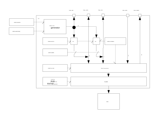
The I2S protocol specification defines two modes of operation, Master and Slave.
The I2S mode decides which of the two sides (Master or Slave) shall provide the clock signals LRCK and SCK, and these signals are always supplied by the Master to the Slave.
Transmitting and receiving
The I2S module supports both transmission (TX) and reception (RX) of serial data. In both cases the serial data is shifted synchronously to the clock signals SCK and LRCK.
TX data is written to the SDOUT pin on the falling edge of SCK, and RX data is read from the SDIN pin on the rising edge of SCK. The most significant bit (MSB) is always transmitted first.
TX and RX are available in both Master and Slave modes and can be enabled/disabled independently in the CONFIG.TXEN and CONFIG.RXEN.
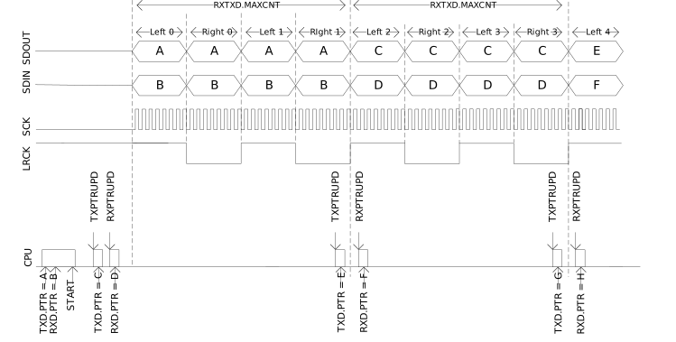
Transmission and/or reception is started by triggering the START task. When started and transmission is enabled (in CONFIG.TXEN), the TXPTRUPD event will be generated for every RXTXD.MAXCNT number of transmitted data words (containing one or more samples). Similarly, when started and reception is enabled (in CONFIG.RXEN), the RXPTRUPD event will be generated for every RXTXD.MAXCNT received data words.
Left right clock (LRCK)
The Left Right Clock (LRCK), often referred to as "word clock", "sample clock" or "word select" in I2S context, is the clock defining the frames in the serial bit streams sent and received on SDOUT and SDIN, respectively.
In I2S mode, each frame contains one left and right sample pair, with the left sample being transferred during the low half period of LRCK followed by the right sample being transferred during the high period of LRCK.
In Aligned mode, each frame contains one left and right sample pair, with the left sample being transferred during the high half period of LRCK followed by the right sample being transferred during the low period of LRCK.
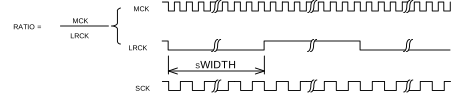
Consequently, the LRCK frequency is equivalent to the audio sample rate.
LRCK = MCK / CONFIG.RATIO
LRCK always toggles around the falling edge of the serial clock SCK.
Serial clock (SCK)
The serial clock (SCK), often referred to as the serial bit clock, pulses once for each data bit being transferred on the serial data lines SDIN and SDOUT.
SCK = 2 * LRCK * CONFIG.SWIDTH
The falling edge of the SCK falls on the toggling edge of LRCK.
When operating in Slave mode SCK is provided by the external I2S master.
Master clock (MCK)
The master clock (MCK) is the clock from which LRCK and SCK are derived when operating in Master mode.
The MCK is generated by an internal MCK generator. This generator always needs to be enabled when in Master mode, but the generator can also be enabled when in Slave mode. Enabling the generator when in slave mode can be useful in the case where the external Master is not able to generate its own master clock.
The MCK generator is enabled/disabled in the register CONFIG.MCKEN, and the generator is started or stopped by the START or STOP tasks.
In Master mode the LRCK and the SCK frequencies are closely related, as both are derived from MCK and set indirectly through CONFIG.RATIO and CONFIG.SWIDTH.
When configuring these registers, the user is responsible for fulfilling the following requirements:
- SCK frequency can never exceed the MCK frequency, which can be formulated
as:
CONFIG.RATIO >= 2 * CONFIG.SWIDTH
- The MCK/LRCK ratio shall be a multiple of 2 * CONFIG.SWIDTH, which can be formulated as:
Integer = (CONFIG.RATIO / (2 * CONFIG.SWIDTH))
The MCK signal can be routed to an output pin (specified in PSEL.MCK) to supply external I2S devices that require the MCK to be supplied from the outside.
When operating in Slave mode, the I2S module does not use the MCK and the MCK generator does not need to be enabled.
| Desired LRCK [Hz] | CONFIG.SWIDTH | CONFIG.RATIO | CONFIG.MCKFREQ | MCK [Hz] | LRCK [Hz] | LRCK error [%] |
|---|---|---|---|---|---|---|
| 16000 | 16Bit | 32X | 32MDIV63 | 507936.5 | 15873.0 | -0.8 |
| 16000 | 16Bit | 64X | 32MDIV31 | 1032258.1 | 16129.0 | 0.8 |
| 16000 | 16Bit | 256X | 32MDIV8 | 4000000.0 | 15625.0 | -2.3 |
| 32000 | 16Bit | 32X | 32MDIV31 | 1032258.1 | 32258.1 | 0.8 |
| 32000 | 16Bit | 64X | 32MDIV16 | 2000000.0 | 31250.0 | -2.3 |
| 32000 | 16Bit | 256X | 32MDIV4 | 8000000.0 | 31250.0 | -2.3 |
| 44100 | 16Bit | 32X | 32MDIV23 | 1391304.3 | 43478.3 | -1.4 |
| 44100 | 16Bit | 64X | 32MDIV11 | 2909090.9 | 45454.5 | 3.1 |
| 44100 | 16Bit | 256X | 32MDIV3 | 10666666.7 | 41666.7 | -5.5 |
Width, alignment and format
The CONFIG.SWIDTH register primarily defines the sample width of the data written to memory. In master mode, it then also sets the amount of bits per frame. In Slave mode it controls padding/trimming if required. Left, right, transmitted, and received samples always have the same width. The CONFIG.FORMAT register specifies the position of the data frames with respect to the LRCK edges in both Master and Slave modes.
When using I2S format, the first bit in a half-frame (containing one left or right sample) gets sampled on the second rising edge of the SCK after a LRCK edge. When using Aligned mode, the first bit in a half-frame gets sampled on the first rising edge of SCK following a LRCK edge.
For data being received on SDIN the sample value can be either right or left-aligned inside a half-frame, as specified in CONFIG.ALIGN. CONFIG.ALIGN affects only the decoding of the incoming samples (SDIN), while the outgoing samples (SDOUT) are always left-aligned (or justified).
When using left-alignment, each half-frame starts with the MSB of the sample value (both for data being sent on SDOUT and received on SDIN).
When using right-alignment, each half-frame of data being received on SDIN ends with the LSB of the sample value, while each half-frame of data being sent on SDOUT starts with the MSB of the sample value (same as for left-alignment).
In Master mode, the size of a half-frame (in number of SCK periods) equals the sample width (in number of bits), and in this case the alignment setting does not care as each half-frame in any case will start with the MSB and end with the LSB of the sample value.
In slave mode, however, the sample width does not need to equal the frame size. This means you might have extra or fewer SCK pulses per half-frame than what the sample width specified in CONFIG.SWIDTH requires.
In the case where we use left-alignment and the number of SCK pulses per half-frame is higher than the sample width, the following will apply:
- For data received on SDIN, all bits after the LSB of the sample value will be discarded.
- For data sent on SDOUT, all bits after the LSB of the sample value will be 0.
In the case where we use left-alignment and the number of SCK pulses per frame is lower than the sample width, the following will apply:
- Data sent and received on SDOUT and SDIN will be truncated with the LSBs being removed first.
- For data received on SDIN, all bits before the MSB of the sample value will be discarded.
- For data sent on SDOUT, all bits after the LSB of the sample value will be 0 (same behavior as for left-alignment).
In the case where we use right-alignment and the number of SCK pulses per frame is lower than the sample width, the following will apply:
- Data received on SDIN will be sign-extended to "sample width" number of bits before being written to memory.
- Data sent on SDOUT will be truncated with the LSBs being removed first (same behavior as for left-alignment).


EasyDMA
The I2S module implements EasyDMA for accessing internal Data RAM without CPU intervention.
The source and destination pointers for the TX and RX data are configured in TXD.PTR and RXD.PTR. The memory pointed to by these pointers will only be read or written when TX or RX are enabled in CONFIG.TXEN and CONFIG.RXEN.
The addresses written to the pointer registers TXD.PTR and RXD.PTR are double-buffered in hardware, and these double buffers are updated for every RXTXD.MAXCNT words (containing one or more samples) read/written from/to memory. The events TXPTRUPD and RXPTRUPD are generated whenever the TXD.PTR and RXD.PTR are transferred to these double buffers.
If TXD.PTR is not pointing to the Data RAM region when transmission is enabled, or RXD.PTR is not pointing to the Data RAM region when reception is enabled, an EasyDMA transfer may result in a HardFault and/or memory corruption. See Memory for more information about the different memory regions.
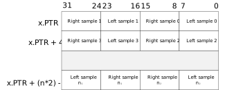
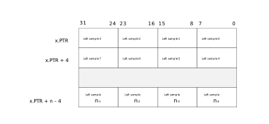
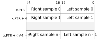
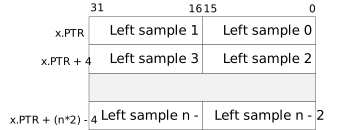
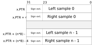
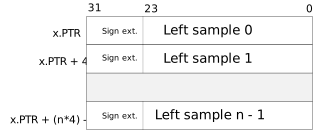
Due to the nature of I2S, where the number of transmitted samples always equals the number of received samples (at least when both TX and RX are enabled), one common register RXTXD.MAXCNT is used for specifying the sizes of these two memory buffers. The size of the buffers is specified in a number of 32-bit words. Such a 32-bit memory word can either contain four 8-bit samples, two 16-bit samples or one right-aligned 24-bit sample sign extended to 32 bit.
In stereo mode (CONFIG.CHANNELS=Stereo), the samples are stored as "left and right sample pairs" in memory. Figure Figure 6, Figure 8 and Figure 10 show how the samples are mapped to memory in this mode. The mapping is valid for both RX and TX.
In mono mode (CONFIG.CHANNELS=Left or Right), RX sample from only one channel in the frame is stored in memory, the other channel sample is ignored. Illustrations Figure 7, Figure 9 and Figure 11 show how RX samples are mapped to memory in this mode.
For TX, the same outgoing sample read from memory is transmitted on both left and right in a frame, resulting in a mono output stream.
Module operation
Described here is a typical operating procedure for the I2S module.
Pin configuration
The MCK, SCK, LRCK, SDIN and SDOUT signals associated with the I2S module are mapped to physical pins according to the pin numbers specified in the PSEL.x registers.
These pins are acquired whenever the I2S module is enabled through the register ENABLE.
When a pin is acquired by the I2S module, the direction of the pin (input or output) will be configured automatically, and any pin direction setting done in the GPIO module will be overridden. The directions for the various I2S pins are shown below in Table 2 and Table 3.
To secure correct signal levels on the pins when the system is in OFF mode, and when the I2S module is disabled, these pins must be configured in the GPIO peripheral directly.
| I2S signal | I2S pin | Direction | Output value | Comment |
|---|---|---|---|---|
| MCK | As specified in PSEL.MCK | Output | 0 | |
| LRCK | As specified in PSEL.LRCK | Output | 0 | |
| SCK | As specified in PSEL.SCK | Output | 0 | |
| SDIN | As specified in PSEL.SDIN | Input | Not applicable | |
| SDOUT | As specified in PSEL.SDOUT | Output | 0 |
| I2S signal | I2S pin | Direction | Output value | Comment |
|---|---|---|---|---|
| MCK | As specified in PSEL.MCK | Output | 0 | |
| LRCK | As specified in PSEL.LRCK | Input | Not applicable | |
| SCK | As specified in PSEL.SCK | Input | Not applicable | |
| SDIN | As specified in PSEL.SDIN | Input | Not applicable | |
| SDOUT | As specified in PSEL.SDOUT | Output | 0 |
Registers
| Base address | Peripheral | Instance | Description | Configuration | |
|---|---|---|---|---|---|
| 0x40025000 | I2S | I2S | Inter-IC Sound Interface | ||
| Register | Offset | Description | |
|---|---|---|---|
| TASKS_START | 0x000 | Starts continuous I2S transfer. Also starts MCK generator when this is enabled. | |
| TASKS_STOP | 0x004 | Stops I2S transfer. Also stops MCK generator. Triggering this task will cause the {event:STOPPED} event to be generated. | |
| EVENTS_RXPTRUPD | 0x104 | The RXD.PTR register has been copied to internal double-buffers. When the I2S module is started and RX is enabled, this event will be generated for every RXTXD.MAXCNT words that are received on the SDIN pin. | |
| EVENTS_STOPPED | 0x108 | I2S transfer stopped. | |
| EVENTS_TXPTRUPD | 0x114 | The TDX.PTR register has been copied to internal double-buffers. When the I2S module is started and TX is enabled, this event will be generated for every RXTXD.MAXCNT words that are sent on the SDOUT pin. | |
| INTEN | 0x300 | Enable or disable interrupt | |
| INTENSET | 0x304 | Enable interrupt | |
| INTENCLR | 0x308 | Disable interrupt | |
| ENABLE | 0x500 | Enable I2S module. | |
| CONFIG.MODE | 0x504 | I2S mode. | |
| CONFIG.RXEN | 0x508 | Reception (RX) enable. | |
| CONFIG.TXEN | 0x50C | Transmission (TX) enable. | |
| CONFIG.MCKEN | 0x510 | Master clock generator enable. | |
| CONFIG.MCKFREQ | 0x514 | Master clock generator frequency. | |
| CONFIG.RATIO | 0x518 | MCK / LRCK ratio. | |
| CONFIG.SWIDTH | 0x51C | Sample width. | |
| CONFIG.ALIGN | 0x520 | Alignment of sample within a frame. | |
| CONFIG.FORMAT | 0x524 | Frame format. | |
| CONFIG.CHANNELS | 0x528 | Enable channels. | |
| RXD.PTR | 0x538 | Receive buffer RAM start address. | |
| TXD.PTR | 0x540 | Transmit buffer RAM start address. | |
| RXTXD.MAXCNT | 0x550 | Size of RXD and TXD buffers. | |
| PSEL.MCK | 0x560 | Pin select for MCK signal. | |
| PSEL.SCK | 0x564 | Pin select for SCK signal. | |
| PSEL.LRCK | 0x568 | Pin select for LRCK signal. | |
| PSEL.SDIN | 0x56C | Pin select for SDIN signal. | |
| PSEL.SDOUT | 0x570 | Pin select for SDOUT signal. | |
INTEN
Address offset: 0x300
Enable or disable interrupt
| Bit number | 31 | 30 | 29 | 28 | 27 | 26 | 25 | 24 | 23 | 22 | 21 | 20 | 19 | 18 | 17 | 16 | 15 | 14 | 13 | 12 | 11 | 10 | 9 | 8 | 7 | 6 | 5 | 4 | 3 | 2 | 1 | 0 | |||
|---|---|---|---|---|---|---|---|---|---|---|---|---|---|---|---|---|---|---|---|---|---|---|---|---|---|---|---|---|---|---|---|---|---|---|---|
| Id | F | C | B | ||||||||||||||||||||||||||||||||
| Reset 0x00000000 | 0 | 0 | 0 | 0 | 0 | 0 | 0 | 0 | 0 | 0 | 0 | 0 | 0 | 0 | 0 | 0 | 0 | 0 | 0 | 0 | 0 | 0 | 0 | 0 | 0 | 0 | 0 | 0 | 0 | 0 | 0 | 0 | |||
| Id | RW | Field | Value Id | Value | Description | ||||||||||||||||||||||||||||||
| B | RW | RXPTRUPD | Enable or disable interrupt for RXPTRUPD event See EVENTS_RXPTRUPD | ||||||||||||||||||||||||||||||||
Disabled | 0 | Disable | |||||||||||||||||||||||||||||||||
Enabled | 1 | Enable | |||||||||||||||||||||||||||||||||
| C | RW | STOPPED | Enable or disable interrupt for STOPPED event See EVENTS_STOPPED | ||||||||||||||||||||||||||||||||
Disabled | 0 | Disable | |||||||||||||||||||||||||||||||||
Enabled | 1 | Enable | |||||||||||||||||||||||||||||||||
| F | RW | TXPTRUPD | Enable or disable interrupt for TXPTRUPD event See EVENTS_TXPTRUPD | ||||||||||||||||||||||||||||||||
Disabled | 0 | Disable | |||||||||||||||||||||||||||||||||
Enabled | 1 | Enable | |||||||||||||||||||||||||||||||||
INTENSET
Address offset: 0x304
Enable interrupt
| Bit number | 31 | 30 | 29 | 28 | 27 | 26 | 25 | 24 | 23 | 22 | 21 | 20 | 19 | 18 | 17 | 16 | 15 | 14 | 13 | 12 | 11 | 10 | 9 | 8 | 7 | 6 | 5 | 4 | 3 | 2 | 1 | 0 | |||
|---|---|---|---|---|---|---|---|---|---|---|---|---|---|---|---|---|---|---|---|---|---|---|---|---|---|---|---|---|---|---|---|---|---|---|---|
| Id | F | C | B | ||||||||||||||||||||||||||||||||
| Reset 0x00000000 | 0 | 0 | 0 | 0 | 0 | 0 | 0 | 0 | 0 | 0 | 0 | 0 | 0 | 0 | 0 | 0 | 0 | 0 | 0 | 0 | 0 | 0 | 0 | 0 | 0 | 0 | 0 | 0 | 0 | 0 | 0 | 0 | |||
| Id | RW | Field | Value Id | Value | Description | ||||||||||||||||||||||||||||||
| B | RW | RXPTRUPD | Write '1' to Enable interrupt for RXPTRUPD event See EVENTS_RXPTRUPD | ||||||||||||||||||||||||||||||||
Set | 1 | Enable | |||||||||||||||||||||||||||||||||
Disabled | 0 | Read: Disabled | |||||||||||||||||||||||||||||||||
Enabled | 1 | Read: Enabled | |||||||||||||||||||||||||||||||||
| C | RW | STOPPED | Write '1' to Enable interrupt for STOPPED event See EVENTS_STOPPED | ||||||||||||||||||||||||||||||||
Set | 1 | Enable | |||||||||||||||||||||||||||||||||
Disabled | 0 | Read: Disabled | |||||||||||||||||||||||||||||||||
Enabled | 1 | Read: Enabled | |||||||||||||||||||||||||||||||||
| F | RW | TXPTRUPD | Write '1' to Enable interrupt for TXPTRUPD event See EVENTS_TXPTRUPD | ||||||||||||||||||||||||||||||||
Set | 1 | Enable | |||||||||||||||||||||||||||||||||
Disabled | 0 | Read: Disabled | |||||||||||||||||||||||||||||||||
Enabled | 1 | Read: Enabled | |||||||||||||||||||||||||||||||||
INTENCLR
Address offset: 0x308
Disable interrupt
| Bit number | 31 | 30 | 29 | 28 | 27 | 26 | 25 | 24 | 23 | 22 | 21 | 20 | 19 | 18 | 17 | 16 | 15 | 14 | 13 | 12 | 11 | 10 | 9 | 8 | 7 | 6 | 5 | 4 | 3 | 2 | 1 | 0 | |||
|---|---|---|---|---|---|---|---|---|---|---|---|---|---|---|---|---|---|---|---|---|---|---|---|---|---|---|---|---|---|---|---|---|---|---|---|
| Id | F | C | B | ||||||||||||||||||||||||||||||||
| Reset 0x00000000 | 0 | 0 | 0 | 0 | 0 | 0 | 0 | 0 | 0 | 0 | 0 | 0 | 0 | 0 | 0 | 0 | 0 | 0 | 0 | 0 | 0 | 0 | 0 | 0 | 0 | 0 | 0 | 0 | 0 | 0 | 0 | 0 | |||
| Id | RW | Field | Value Id | Value | Description | ||||||||||||||||||||||||||||||
| B | RW | RXPTRUPD | Write '1' to Disable interrupt for RXPTRUPD event See EVENTS_RXPTRUPD | ||||||||||||||||||||||||||||||||
Clear | 1 | Disable | |||||||||||||||||||||||||||||||||
Disabled | 0 | Read: Disabled | |||||||||||||||||||||||||||||||||
Enabled | 1 | Read: Enabled | |||||||||||||||||||||||||||||||||
| C | RW | STOPPED | Write '1' to Disable interrupt for STOPPED event See EVENTS_STOPPED | ||||||||||||||||||||||||||||||||
Clear | 1 | Disable | |||||||||||||||||||||||||||||||||
Disabled | 0 | Read: Disabled | |||||||||||||||||||||||||||||||||
Enabled | 1 | Read: Enabled | |||||||||||||||||||||||||||||||||
| F | RW | TXPTRUPD | Write '1' to Disable interrupt for TXPTRUPD event See EVENTS_TXPTRUPD | ||||||||||||||||||||||||||||||||
Clear | 1 | Disable | |||||||||||||||||||||||||||||||||
Disabled | 0 | Read: Disabled | |||||||||||||||||||||||||||||||||
Enabled | 1 | Read: Enabled | |||||||||||||||||||||||||||||||||
ENABLE
Address offset: 0x500
Enable I2S module.
| Bit number | 31 | 30 | 29 | 28 | 27 | 26 | 25 | 24 | 23 | 22 | 21 | 20 | 19 | 18 | 17 | 16 | 15 | 14 | 13 | 12 | 11 | 10 | 9 | 8 | 7 | 6 | 5 | 4 | 3 | 2 | 1 | 0 | |||
|---|---|---|---|---|---|---|---|---|---|---|---|---|---|---|---|---|---|---|---|---|---|---|---|---|---|---|---|---|---|---|---|---|---|---|---|
| Id | A | ||||||||||||||||||||||||||||||||||
| Reset 0x00000000 | 0 | 0 | 0 | 0 | 0 | 0 | 0 | 0 | 0 | 0 | 0 | 0 | 0 | 0 | 0 | 0 | 0 | 0 | 0 | 0 | 0 | 0 | 0 | 0 | 0 | 0 | 0 | 0 | 0 | 0 | 0 | 0 | |||
| Id | RW | Field | Value Id | Value | Description | ||||||||||||||||||||||||||||||
| A | RW | ENABLE | Enable I2S module. | ||||||||||||||||||||||||||||||||
Disabled | 0 | Disable | |||||||||||||||||||||||||||||||||
Enabled | 1 | Enable | |||||||||||||||||||||||||||||||||
CONFIG.MODE
Address offset: 0x504
I2S mode.
| Bit number | 31 | 30 | 29 | 28 | 27 | 26 | 25 | 24 | 23 | 22 | 21 | 20 | 19 | 18 | 17 | 16 | 15 | 14 | 13 | 12 | 11 | 10 | 9 | 8 | 7 | 6 | 5 | 4 | 3 | 2 | 1 | 0 | |||
|---|---|---|---|---|---|---|---|---|---|---|---|---|---|---|---|---|---|---|---|---|---|---|---|---|---|---|---|---|---|---|---|---|---|---|---|
| Id | A | ||||||||||||||||||||||||||||||||||
| Reset 0x00000000 | 0 | 0 | 0 | 0 | 0 | 0 | 0 | 0 | 0 | 0 | 0 | 0 | 0 | 0 | 0 | 0 | 0 | 0 | 0 | 0 | 0 | 0 | 0 | 0 | 0 | 0 | 0 | 0 | 0 | 0 | 0 | 0 | |||
| Id | RW | Field | Value Id | Value | Description | ||||||||||||||||||||||||||||||
| A | RW | MODE | I2S mode. | ||||||||||||||||||||||||||||||||
Master | 0 | Master mode. SCK and LRCK generated from internal master clcok (MCK) and output on pins defined by PSEL.xxx. | |||||||||||||||||||||||||||||||||
Slave | 1 | Slave mode. SCK and LRCK generated by external master and received on pins defined by PSEL.xxx | |||||||||||||||||||||||||||||||||
CONFIG.RXEN
Address offset: 0x508
Reception (RX) enable.
| Bit number | 31 | 30 | 29 | 28 | 27 | 26 | 25 | 24 | 23 | 22 | 21 | 20 | 19 | 18 | 17 | 16 | 15 | 14 | 13 | 12 | 11 | 10 | 9 | 8 | 7 | 6 | 5 | 4 | 3 | 2 | 1 | 0 | |||
|---|---|---|---|---|---|---|---|---|---|---|---|---|---|---|---|---|---|---|---|---|---|---|---|---|---|---|---|---|---|---|---|---|---|---|---|
| Id | A | ||||||||||||||||||||||||||||||||||
| Reset 0x00000000 | 0 | 0 | 0 | 0 | 0 | 0 | 0 | 0 | 0 | 0 | 0 | 0 | 0 | 0 | 0 | 0 | 0 | 0 | 0 | 0 | 0 | 0 | 0 | 0 | 0 | 0 | 0 | 0 | 0 | 0 | 0 | 0 | |||
| Id | RW | Field | Value Id | Value | Description | ||||||||||||||||||||||||||||||
| A | RW | RXEN | Reception (RX) enable. | ||||||||||||||||||||||||||||||||
Disabled | 0 | Reception disabled and now data will be written to the RXD.PTR address. | |||||||||||||||||||||||||||||||||
Enabled | 1 | Reception enabled. | |||||||||||||||||||||||||||||||||
CONFIG.TXEN
Address offset: 0x50C
Transmission (TX) enable.
| Bit number | 31 | 30 | 29 | 28 | 27 | 26 | 25 | 24 | 23 | 22 | 21 | 20 | 19 | 18 | 17 | 16 | 15 | 14 | 13 | 12 | 11 | 10 | 9 | 8 | 7 | 6 | 5 | 4 | 3 | 2 | 1 | 0 | |||
|---|---|---|---|---|---|---|---|---|---|---|---|---|---|---|---|---|---|---|---|---|---|---|---|---|---|---|---|---|---|---|---|---|---|---|---|
| Id | A | ||||||||||||||||||||||||||||||||||
| Reset 0x00000001 | 0 | 0 | 0 | 0 | 0 | 0 | 0 | 0 | 0 | 0 | 0 | 0 | 0 | 0 | 0 | 0 | 0 | 0 | 0 | 0 | 0 | 0 | 0 | 0 | 0 | 0 | 0 | 0 | 0 | 0 | 0 | 1 | |||
| Id | RW | Field | Value Id | Value | Description | ||||||||||||||||||||||||||||||
| A | RW | TXEN | Transmission (TX) enable. | ||||||||||||||||||||||||||||||||
Disabled | 0 | Transmission disabled and now data will be read from the RXD.TXD address. | |||||||||||||||||||||||||||||||||
Enabled | 1 | Transmission enabled. | |||||||||||||||||||||||||||||||||
CONFIG.MCKEN
Address offset: 0x510
Master clock generator enable.
| Bit number | 31 | 30 | 29 | 28 | 27 | 26 | 25 | 24 | 23 | 22 | 21 | 20 | 19 | 18 | 17 | 16 | 15 | 14 | 13 | 12 | 11 | 10 | 9 | 8 | 7 | 6 | 5 | 4 | 3 | 2 | 1 | 0 | |||
|---|---|---|---|---|---|---|---|---|---|---|---|---|---|---|---|---|---|---|---|---|---|---|---|---|---|---|---|---|---|---|---|---|---|---|---|
| Id | A | ||||||||||||||||||||||||||||||||||
| Reset 0x00000001 | 0 | 0 | 0 | 0 | 0 | 0 | 0 | 0 | 0 | 0 | 0 | 0 | 0 | 0 | 0 | 0 | 0 | 0 | 0 | 0 | 0 | 0 | 0 | 0 | 0 | 0 | 0 | 0 | 0 | 0 | 0 | 1 | |||
| Id | RW | Field | Value Id | Value | Description | ||||||||||||||||||||||||||||||
| A | RW | MCKEN | Master clock generator enable. | ||||||||||||||||||||||||||||||||
Disabled | 0 | Master clock generator disabled and PSEL.MCK not connected(available as GPIO). | |||||||||||||||||||||||||||||||||
Enabled | 1 | Master clock generator running and MCK output on PSEL.MCK. | |||||||||||||||||||||||||||||||||
CONFIG.MCKFREQ
Address offset: 0x514
Master clock generator frequency.
| Bit number | 31 | 30 | 29 | 28 | 27 | 26 | 25 | 24 | 23 | 22 | 21 | 20 | 19 | 18 | 17 | 16 | 15 | 14 | 13 | 12 | 11 | 10 | 9 | 8 | 7 | 6 | 5 | 4 | 3 | 2 | 1 | 0 | |||
|---|---|---|---|---|---|---|---|---|---|---|---|---|---|---|---|---|---|---|---|---|---|---|---|---|---|---|---|---|---|---|---|---|---|---|---|
| Id | A | A | A | A | A | A | A | A | A | A | A | A | A | A | A | A | A | A | A | A | A | A | A | A | A | A | A | A | A | A | A | A | |||
| Reset 0x20000000 | 0 | 0 | 1 | 0 | 0 | 0 | 0 | 0 | 0 | 0 | 0 | 0 | 0 | 0 | 0 | 0 | 0 | 0 | 0 | 0 | 0 | 0 | 0 | 0 | 0 | 0 | 0 | 0 | 0 | 0 | 0 | 0 | |||
| Id | RW | Field | Value Id | Value | Description | ||||||||||||||||||||||||||||||
| A | RW | MCKFREQ | Master clock generator frequency. | ||||||||||||||||||||||||||||||||
32MDIV2 | 0x80000000 | 32 MHz / 2 = 16.0 MHz | |||||||||||||||||||||||||||||||||
32MDIV3 | 0x50000000 | 32 MHz / 3 = 10.6666667 MHz | |||||||||||||||||||||||||||||||||
32MDIV4 | 0x40000000 | 32 MHz / 4 = 8.0 MHz | |||||||||||||||||||||||||||||||||
32MDIV5 | 0x30000000 | 32 MHz / 5 = 6.4 MHz | |||||||||||||||||||||||||||||||||
32MDIV6 | 0x28000000 | 32 MHz / 6 = 5.3333333 MHz | |||||||||||||||||||||||||||||||||
32MDIV8 | 0x20000000 | 32 MHz / 8 = 4.0 MHz | |||||||||||||||||||||||||||||||||
32MDIV10 | 0x18000000 | 32 MHz / 10 = 3.2 MHz | |||||||||||||||||||||||||||||||||
32MDIV11 | 0x16000000 | 32 MHz / 11 = 2.9090909 MHz | |||||||||||||||||||||||||||||||||
32MDIV15 | 0x11000000 | 32 MHz / 15 = 2.1333333 MHz | |||||||||||||||||||||||||||||||||
32MDIV16 | 0x10000000 | 32 MHz / 16 = 2.0 MHz | |||||||||||||||||||||||||||||||||
32MDIV21 | 0x0C000000 | 32 MHz / 21 = 1.5238095 | |||||||||||||||||||||||||||||||||
32MDIV23 | 0x0B000000 | 32 MHz / 23 = 1.3913043 MHz | |||||||||||||||||||||||||||||||||
32MDIV30 | 0x08800000 | 32 MHz / 30 = 1.0666667 MHz | |||||||||||||||||||||||||||||||||
32MDIV31 | 0x08400000 | 32 MHz / 31 = 1.0322581 MHz | |||||||||||||||||||||||||||||||||
32MDIV32 | 0x08000000 | 32 MHz / 32 = 1.0 MHz | |||||||||||||||||||||||||||||||||
32MDIV42 | 0x06000000 | 32 MHz / 42 = 0.7619048 MHz | |||||||||||||||||||||||||||||||||
32MDIV63 | 0x04100000 | 32 MHz / 63 = 0.5079365 MHz | |||||||||||||||||||||||||||||||||
32MDIV125 | 0x020C0000 | 32 MHz / 125 = 0.256 MHz | |||||||||||||||||||||||||||||||||
CONFIG.RATIO
Address offset: 0x518
MCK / LRCK ratio.
| Bit number | 31 | 30 | 29 | 28 | 27 | 26 | 25 | 24 | 23 | 22 | 21 | 20 | 19 | 18 | 17 | 16 | 15 | 14 | 13 | 12 | 11 | 10 | 9 | 8 | 7 | 6 | 5 | 4 | 3 | 2 | 1 | 0 | |||
|---|---|---|---|---|---|---|---|---|---|---|---|---|---|---|---|---|---|---|---|---|---|---|---|---|---|---|---|---|---|---|---|---|---|---|---|
| Id | A | A | A | A | |||||||||||||||||||||||||||||||
| Reset 0x00000006 | 0 | 0 | 0 | 0 | 0 | 0 | 0 | 0 | 0 | 0 | 0 | 0 | 0 | 0 | 0 | 0 | 0 | 0 | 0 | 0 | 0 | 0 | 0 | 0 | 0 | 0 | 0 | 0 | 0 | 1 | 1 | 0 | |||
| Id | RW | Field | Value Id | Value | Description | ||||||||||||||||||||||||||||||
| A | RW | RATIO | MCK / LRCK ratio. | ||||||||||||||||||||||||||||||||
32X | 0 | LRCK = MCK / 32 | |||||||||||||||||||||||||||||||||
48X | 1 | LRCK = MCK / 48 | |||||||||||||||||||||||||||||||||
64X | 2 | LRCK = MCK / 64 | |||||||||||||||||||||||||||||||||
96X | 3 | LRCK = MCK / 96 | |||||||||||||||||||||||||||||||||
128X | 4 | LRCK = MCK / 128 | |||||||||||||||||||||||||||||||||
192X | 5 | LRCK = MCK / 192 | |||||||||||||||||||||||||||||||||
256X | 6 | LRCK = MCK / 256 | |||||||||||||||||||||||||||||||||
384X | 7 | LRCK = MCK / 384 | |||||||||||||||||||||||||||||||||
512X | 8 | LRCK = MCK / 512 | |||||||||||||||||||||||||||||||||
CONFIG.SWIDTH
Address offset: 0x51C
Sample width.
| Bit number | 31 | 30 | 29 | 28 | 27 | 26 | 25 | 24 | 23 | 22 | 21 | 20 | 19 | 18 | 17 | 16 | 15 | 14 | 13 | 12 | 11 | 10 | 9 | 8 | 7 | 6 | 5 | 4 | 3 | 2 | 1 | 0 | |||
|---|---|---|---|---|---|---|---|---|---|---|---|---|---|---|---|---|---|---|---|---|---|---|---|---|---|---|---|---|---|---|---|---|---|---|---|
| Id | A | A | |||||||||||||||||||||||||||||||||
| Reset 0x00000001 | 0 | 0 | 0 | 0 | 0 | 0 | 0 | 0 | 0 | 0 | 0 | 0 | 0 | 0 | 0 | 0 | 0 | 0 | 0 | 0 | 0 | 0 | 0 | 0 | 0 | 0 | 0 | 0 | 0 | 0 | 0 | 1 | |||
| Id | RW | Field | Value Id | Value | Description | ||||||||||||||||||||||||||||||
| A | RW | SWIDTH | Sample width. | ||||||||||||||||||||||||||||||||
8Bit | 0 | 8 bit. | |||||||||||||||||||||||||||||||||
16Bit | 1 | 16 bit. | |||||||||||||||||||||||||||||||||
24Bit | 2 | 24 bit. | |||||||||||||||||||||||||||||||||
CONFIG.ALIGN
Address offset: 0x520
Alignment of sample within a frame.
| Bit number | 31 | 30 | 29 | 28 | 27 | 26 | 25 | 24 | 23 | 22 | 21 | 20 | 19 | 18 | 17 | 16 | 15 | 14 | 13 | 12 | 11 | 10 | 9 | 8 | 7 | 6 | 5 | 4 | 3 | 2 | 1 | 0 | |||
|---|---|---|---|---|---|---|---|---|---|---|---|---|---|---|---|---|---|---|---|---|---|---|---|---|---|---|---|---|---|---|---|---|---|---|---|
| Id | A | ||||||||||||||||||||||||||||||||||
| Reset 0x00000000 | 0 | 0 | 0 | 0 | 0 | 0 | 0 | 0 | 0 | 0 | 0 | 0 | 0 | 0 | 0 | 0 | 0 | 0 | 0 | 0 | 0 | 0 | 0 | 0 | 0 | 0 | 0 | 0 | 0 | 0 | 0 | 0 | |||
| Id | RW | Field | Value Id | Value | Description | ||||||||||||||||||||||||||||||
| A | RW | ALIGN | Alignment of sample within a frame. | ||||||||||||||||||||||||||||||||
Left | 0 | Left-aligned. | |||||||||||||||||||||||||||||||||
Right | 1 | Right-aligned. | |||||||||||||||||||||||||||||||||
CONFIG.FORMAT
Address offset: 0x524
Frame format.
| Bit number | 31 | 30 | 29 | 28 | 27 | 26 | 25 | 24 | 23 | 22 | 21 | 20 | 19 | 18 | 17 | 16 | 15 | 14 | 13 | 12 | 11 | 10 | 9 | 8 | 7 | 6 | 5 | 4 | 3 | 2 | 1 | 0 | |||
|---|---|---|---|---|---|---|---|---|---|---|---|---|---|---|---|---|---|---|---|---|---|---|---|---|---|---|---|---|---|---|---|---|---|---|---|
| Id | A | ||||||||||||||||||||||||||||||||||
| Reset 0x00000000 | 0 | 0 | 0 | 0 | 0 | 0 | 0 | 0 | 0 | 0 | 0 | 0 | 0 | 0 | 0 | 0 | 0 | 0 | 0 | 0 | 0 | 0 | 0 | 0 | 0 | 0 | 0 | 0 | 0 | 0 | 0 | 0 | |||
| Id | RW | Field | Value Id | Value | Description | ||||||||||||||||||||||||||||||
| A | RW | FORMAT | Frame format. | ||||||||||||||||||||||||||||||||
I2S | 0 | Original I2S format. | |||||||||||||||||||||||||||||||||
Aligned | 1 | Alternate (left- or right-aligned) format. | |||||||||||||||||||||||||||||||||
CONFIG.CHANNELS
Address offset: 0x528
Enable channels.
| Bit number | 31 | 30 | 29 | 28 | 27 | 26 | 25 | 24 | 23 | 22 | 21 | 20 | 19 | 18 | 17 | 16 | 15 | 14 | 13 | 12 | 11 | 10 | 9 | 8 | 7 | 6 | 5 | 4 | 3 | 2 | 1 | 0 | |||
|---|---|---|---|---|---|---|---|---|---|---|---|---|---|---|---|---|---|---|---|---|---|---|---|---|---|---|---|---|---|---|---|---|---|---|---|
| Id | A | A | |||||||||||||||||||||||||||||||||
| Reset 0x00000000 | 0 | 0 | 0 | 0 | 0 | 0 | 0 | 0 | 0 | 0 | 0 | 0 | 0 | 0 | 0 | 0 | 0 | 0 | 0 | 0 | 0 | 0 | 0 | 0 | 0 | 0 | 0 | 0 | 0 | 0 | 0 | 0 | |||
| Id | RW | Field | Value Id | Value | Description | ||||||||||||||||||||||||||||||
| A | RW | CHANNELS | Enable channels. | ||||||||||||||||||||||||||||||||
Stereo | 0 | Stereo. | |||||||||||||||||||||||||||||||||
Left | 1 | Left only. | |||||||||||||||||||||||||||||||||
Right | 2 | Right only. | |||||||||||||||||||||||||||||||||
RXD.PTR
Address offset: 0x538
Receive buffer RAM start address.
| Bit number | 31 | 30 | 29 | 28 | 27 | 26 | 25 | 24 | 23 | 22 | 21 | 20 | 19 | 18 | 17 | 16 | 15 | 14 | 13 | 12 | 11 | 10 | 9 | 8 | 7 | 6 | 5 | 4 | 3 | 2 | 1 | 0 | |||
|---|---|---|---|---|---|---|---|---|---|---|---|---|---|---|---|---|---|---|---|---|---|---|---|---|---|---|---|---|---|---|---|---|---|---|---|
| Id | A | A | A | A | A | A | A | A | A | A | A | A | A | A | A | A | A | A | A | A | A | A | A | A | A | A | A | A | A | A | A | A | |||
| Reset 0x00000000 | 0 | 0 | 0 | 0 | 0 | 0 | 0 | 0 | 0 | 0 | 0 | 0 | 0 | 0 | 0 | 0 | 0 | 0 | 0 | 0 | 0 | 0 | 0 | 0 | 0 | 0 | 0 | 0 | 0 | 0 | 0 | 0 | |||
| Id | RW | Field | Value Id | Value | Description | ||||||||||||||||||||||||||||||
| A | RW | PTR | Receive buffer Data RAM start address. When receiving, words containing samples will be written to this address. This address is a word aligned Data RAM address. | ||||||||||||||||||||||||||||||||
TXD.PTR
Address offset: 0x540
Transmit buffer RAM start address.
| Bit number | 31 | 30 | 29 | 28 | 27 | 26 | 25 | 24 | 23 | 22 | 21 | 20 | 19 | 18 | 17 | 16 | 15 | 14 | 13 | 12 | 11 | 10 | 9 | 8 | 7 | 6 | 5 | 4 | 3 | 2 | 1 | 0 | |||
|---|---|---|---|---|---|---|---|---|---|---|---|---|---|---|---|---|---|---|---|---|---|---|---|---|---|---|---|---|---|---|---|---|---|---|---|
| Id | A | A | A | A | A | A | A | A | A | A | A | A | A | A | A | A | A | A | A | A | A | A | A | A | A | A | A | A | A | A | A | A | |||
| Reset 0x00000000 | 0 | 0 | 0 | 0 | 0 | 0 | 0 | 0 | 0 | 0 | 0 | 0 | 0 | 0 | 0 | 0 | 0 | 0 | 0 | 0 | 0 | 0 | 0 | 0 | 0 | 0 | 0 | 0 | 0 | 0 | 0 | 0 | |||
| Id | RW | Field | Value Id | Value | Description | ||||||||||||||||||||||||||||||
| A | RW | PTR | Transmit buffer Data RAM start address. When transmitting, words containing samples will be fetched from this address. This address is a word aligned Data RAM address. | ||||||||||||||||||||||||||||||||
RXTXD.MAXCNT
Address offset: 0x550
Size of RXD and TXD buffers.
| Bit number | 31 | 30 | 29 | 28 | 27 | 26 | 25 | 24 | 23 | 22 | 21 | 20 | 19 | 18 | 17 | 16 | 15 | 14 | 13 | 12 | 11 | 10 | 9 | 8 | 7 | 6 | 5 | 4 | 3 | 2 | 1 | 0 | |||
|---|---|---|---|---|---|---|---|---|---|---|---|---|---|---|---|---|---|---|---|---|---|---|---|---|---|---|---|---|---|---|---|---|---|---|---|
| Id | A | A | A | A | A | A | A | A | A | A | A | A | A | A | |||||||||||||||||||||
| Reset 0x00000000 | 0 | 0 | 0 | 0 | 0 | 0 | 0 | 0 | 0 | 0 | 0 | 0 | 0 | 0 | 0 | 0 | 0 | 0 | 0 | 0 | 0 | 0 | 0 | 0 | 0 | 0 | 0 | 0 | 0 | 0 | 0 | 0 | |||
| Id | RW | Field | Value Id | Value | Description | ||||||||||||||||||||||||||||||
| A | RW | MAXCNT | Size of RXD and TXD buffers in number of 32 bit words. | ||||||||||||||||||||||||||||||||
PSEL.MCK
Address offset: 0x560
Pin select for MCK signal.
| Bit number | 31 | 30 | 29 | 28 | 27 | 26 | 25 | 24 | 23 | 22 | 21 | 20 | 19 | 18 | 17 | 16 | 15 | 14 | 13 | 12 | 11 | 10 | 9 | 8 | 7 | 6 | 5 | 4 | 3 | 2 | 1 | 0 | |||
|---|---|---|---|---|---|---|---|---|---|---|---|---|---|---|---|---|---|---|---|---|---|---|---|---|---|---|---|---|---|---|---|---|---|---|---|
| Id | C | A | A | A | A | A | |||||||||||||||||||||||||||||
| Reset 0xFFFFFFFF | 1 | 1 | 1 | 1 | 1 | 1 | 1 | 1 | 1 | 1 | 1 | 1 | 1 | 1 | 1 | 1 | 1 | 1 | 1 | 1 | 1 | 1 | 1 | 1 | 1 | 1 | 1 | 1 | 1 | 1 | 1 | 1 | |||
| Id | RW | Field | Value Id | Value | Description | ||||||||||||||||||||||||||||||
| A | RW | PIN | [0..31] | Pin number | |||||||||||||||||||||||||||||||
| C | RW | CONNECT | Connection | ||||||||||||||||||||||||||||||||
Disconnected | 1 | Disconnect | |||||||||||||||||||||||||||||||||
Connected | 0 | Connect | |||||||||||||||||||||||||||||||||
PSEL.SCK
Address offset: 0x564
Pin select for SCK signal.
| Bit number | 31 | 30 | 29 | 28 | 27 | 26 | 25 | 24 | 23 | 22 | 21 | 20 | 19 | 18 | 17 | 16 | 15 | 14 | 13 | 12 | 11 | 10 | 9 | 8 | 7 | 6 | 5 | 4 | 3 | 2 | 1 | 0 | |||
|---|---|---|---|---|---|---|---|---|---|---|---|---|---|---|---|---|---|---|---|---|---|---|---|---|---|---|---|---|---|---|---|---|---|---|---|
| Id | C | A | A | A | A | A | |||||||||||||||||||||||||||||
| Reset 0xFFFFFFFF | 1 | 1 | 1 | 1 | 1 | 1 | 1 | 1 | 1 | 1 | 1 | 1 | 1 | 1 | 1 | 1 | 1 | 1 | 1 | 1 | 1 | 1 | 1 | 1 | 1 | 1 | 1 | 1 | 1 | 1 | 1 | 1 | |||
| Id | RW | Field | Value Id | Value | Description | ||||||||||||||||||||||||||||||
| A | RW | PIN | [0..31] | Pin number | |||||||||||||||||||||||||||||||
| C | RW | CONNECT | Connection | ||||||||||||||||||||||||||||||||
Disconnected | 1 | Disconnect | |||||||||||||||||||||||||||||||||
Connected | 0 | Connect | |||||||||||||||||||||||||||||||||
PSEL.LRCK
Address offset: 0x568
Pin select for LRCK signal.
| Bit number | 31 | 30 | 29 | 28 | 27 | 26 | 25 | 24 | 23 | 22 | 21 | 20 | 19 | 18 | 17 | 16 | 15 | 14 | 13 | 12 | 11 | 10 | 9 | 8 | 7 | 6 | 5 | 4 | 3 | 2 | 1 | 0 | |||
|---|---|---|---|---|---|---|---|---|---|---|---|---|---|---|---|---|---|---|---|---|---|---|---|---|---|---|---|---|---|---|---|---|---|---|---|
| Id | C | A | A | A | A | A | |||||||||||||||||||||||||||||
| Reset 0xFFFFFFFF | 1 | 1 | 1 | 1 | 1 | 1 | 1 | 1 | 1 | 1 | 1 | 1 | 1 | 1 | 1 | 1 | 1 | 1 | 1 | 1 | 1 | 1 | 1 | 1 | 1 | 1 | 1 | 1 | 1 | 1 | 1 | 1 | |||
| Id | RW | Field | Value Id | Value | Description | ||||||||||||||||||||||||||||||
| A | RW | PIN | [0..31] | Pin number | |||||||||||||||||||||||||||||||
| C | RW | CONNECT | Connection | ||||||||||||||||||||||||||||||||
Disconnected | 1 | Disconnect | |||||||||||||||||||||||||||||||||
Connected | 0 | Connect | |||||||||||||||||||||||||||||||||
PSEL.SDIN
Address offset: 0x56C
Pin select for SDIN signal.
| Bit number | 31 | 30 | 29 | 28 | 27 | 26 | 25 | 24 | 23 | 22 | 21 | 20 | 19 | 18 | 17 | 16 | 15 | 14 | 13 | 12 | 11 | 10 | 9 | 8 | 7 | 6 | 5 | 4 | 3 | 2 | 1 | 0 | |||
|---|---|---|---|---|---|---|---|---|---|---|---|---|---|---|---|---|---|---|---|---|---|---|---|---|---|---|---|---|---|---|---|---|---|---|---|
| Id | C | A | A | A | A | A | |||||||||||||||||||||||||||||
| Reset 0xFFFFFFFF | 1 | 1 | 1 | 1 | 1 | 1 | 1 | 1 | 1 | 1 | 1 | 1 | 1 | 1 | 1 | 1 | 1 | 1 | 1 | 1 | 1 | 1 | 1 | 1 | 1 | 1 | 1 | 1 | 1 | 1 | 1 | 1 | |||
| Id | RW | Field | Value Id | Value | Description | ||||||||||||||||||||||||||||||
| A | RW | PIN | [0..31] | Pin number | |||||||||||||||||||||||||||||||
| C | RW | CONNECT | Connection | ||||||||||||||||||||||||||||||||
Disconnected | 1 | Disconnect | |||||||||||||||||||||||||||||||||
Connected | 0 | Connect | |||||||||||||||||||||||||||||||||
PSEL.SDOUT
Address offset: 0x570
Pin select for SDOUT signal.
| Bit number | 31 | 30 | 29 | 28 | 27 | 26 | 25 | 24 | 23 | 22 | 21 | 20 | 19 | 18 | 17 | 16 | 15 | 14 | 13 | 12 | 11 | 10 | 9 | 8 | 7 | 6 | 5 | 4 | 3 | 2 | 1 | 0 | |||
|---|---|---|---|---|---|---|---|---|---|---|---|---|---|---|---|---|---|---|---|---|---|---|---|---|---|---|---|---|---|---|---|---|---|---|---|
| Id | C | A | A | A | A | A | |||||||||||||||||||||||||||||
| Reset 0xFFFFFFFF | 1 | 1 | 1 | 1 | 1 | 1 | 1 | 1 | 1 | 1 | 1 | 1 | 1 | 1 | 1 | 1 | 1 | 1 | 1 | 1 | 1 | 1 | 1 | 1 | 1 | 1 | 1 | 1 | 1 | 1 | 1 | 1 | |||
| Id | RW | Field | Value Id | Value | Description | ||||||||||||||||||||||||||||||
| A | RW | PIN | [0..31] | Pin number | |||||||||||||||||||||||||||||||
| C | RW | CONNECT | Connection | ||||||||||||||||||||||||||||||||
Disconnected | 1 | Disconnect | |||||||||||||||||||||||||||||||||
Connected | 0 | Connect | |||||||||||||||||||||||||||||||||
Electrical specification
I2S timing specification
| Symbol | Description | Min. | Typ. | Max. | Units | ||||
|---|---|---|---|---|---|---|---|---|---|
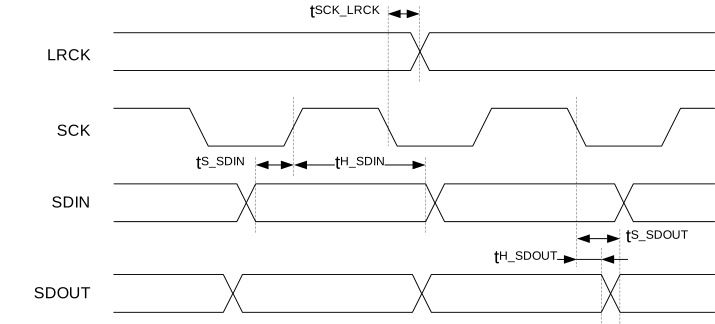
| tS_SDIN | SDIN setup time before SCK rising | 20 | ns | ||||||
| tH_SDIN | SDIN hold time after SCK rising | 15 | ns | ||||||
| tS_SDOUT | SDOUT setup time after SCK falling | 40 | ns | ||||||
| tH_SDOUT | SDOUT hold time before SCK falling | 6 | ns | ||||||
| tSCK_LRCK | SCLK falling to LRCK edge | -5 | 0 | 5 | ns | ||||
| fMCK | MCK frequency | 4000 | kHz | ||||||
| fLRCK | LRCK frequency | 48 | kHz | ||||||
| fSCK | SCK frequency | 2000 | kHz | ||||||
| DCCK | Clock duty cycle (MCK, LRCK, SCK) | 45 | 55 | % |