PWM — Pulse width modulation
The PWM module enables the generation of pulse width modulated signals on GPIO. The module implements an up or up-and-down counter with four PWM channels that drive assigned GPIOs.
Three PWM modules can provide up to 12 PWM channels with individual frequency control in groups of up to four channels. Furthermore, a built-in decoder and EasyDMA capabilities make it possible to manipulate the PWM duty cycles without CPU intervention. Arbitrary duty-cycle sequences are read from Data RAM and can be chained to implement ping-pong buffering or repeated into complex loops.
Listed here are the main features of one PWM module:
- Fixed PWM base frequency with programmable clock divider
- Up to four PWM channels with individual polarity and duty-cycle values
- Edge or center-aligned pulses across PWM channels
- Multiple duty-cycle arrays (sequences) defined in Data RAM
- Autonomous and glitch-free update of duty cycle values directly from memory through EasyDMA
- Change of polarity, duty-cycle, and base frequency possibly on every PWM period
- Data RAM sequences can be repeated or connected into loops
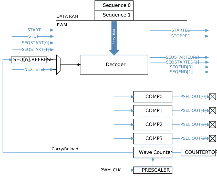
Wave counter
The wave counter is responsible for generating the pulses at a duty-cycle that depends on the compare values, and at a frequency that depends on COUNTERTOP.
There is one common 15-bit counter with four compare channels. Thus, all four channels will share the same period (PWM frequency), but can have individual duty-cycle and polarity. The polarity is set by the value read from RAM (see Figure 4), while the MODE register controls if the counter counts up, or up and down. The timer top value is controlled by the COUNTERTOP register. This register value in conjunction with the selected PRESCALER of the PWM_CLK will result in a given PWM period. A COUNTERTOP value smaller than the compare setting will result in a state where no PWM edges are generated. Respectively, OUT[n] is held high, given that the polarity is set to FallingEdge. All the compare registers are internal and can only be configured through the decoder presented later.
COUNTERTOP can be safely written at any time. It will get sampled following a START task. If DECODER.LOAD is anything else than WaveForm, it will also get sampled following a STARTSEQ[n] task, and when loading a new value from RAM during a sequence playback. If DECODER.LOAD=WaveForm, the register value is ignored, and taken from RAM instead (see Decoder with EasyDMA below).
Figure 2 shows the counter operating in up (MODE=PWM_MODE_Up) mode with three PWM channels with the same frequency but different duty cycle. The counter is automatically reset to zero when COUNTERTOP is reached and OUT[n] will invert. OUT[n] is held low if the compare value is 0 and held high respectively if set to COUNTERTOP given that the polarity is set to FallingEdge. Running in up counter mode will result in pulse widths that are edge-aligned. See the code example below:
uint16_t pwm_seq[4] = {PWM_CH0_DUTY, PWM_CH1_DUTY, PWM_CH2_DUTY, PWM_CH3_DUTY};
NRF_PWM0->PSEL.OUT[0] = (first_pin << PWM_PSEL_OUT_PIN_Pos) |
                        (PWM_PSEL_OUT_CONNECT_Connected <<
                                                 PWM_PSEL_OUT_CONNECT_Pos);
NRF_PWM0->PSEL.OUT[1] = (second_pin << PWM_PSEL_OUT_PIN_Pos) |
                        (PWM_PSEL_OUT_CONNECT_Connected <<
                                                 PWM_PSEL_OUT_CONNECT_Pos);
NRF_PWM0->ENABLE      = (PWM_ENABLE_ENABLE_Enabled << PWM_ENABLE_ENABLE_Pos);
NRF_PWM0->MODE        = (PWM_MODE_UPDOWN_Up << PWM_MODE_UPDOWN_Pos);
NRF_PWM0->PRESCALER   = (PWM_PRESCALER_PRESCALER_DIV_1 <<
                                                 PWM_PRESCALER_PRESCALER_Pos);
NRF_PWM0->COUNTERTOP  = (16000 << PWM_COUNTERTOP_COUNTERTOP_Pos); //1 msec
NRF_PWM0->LOOP        = (PWM_LOOP_CNT_Disabled << PWM_LOOP_CNT_Pos);
NRF_PWM0->DECODER   = (PWM_DECODER_LOAD_Individual << PWM_DECODER_LOAD_Pos) |
                      (PWM_DECODER_MODE_RefreshCount << PWM_DECODER_MODE_Pos);
NRF_PWM0->SEQ[0].PTR  = ((uint32_t)(pwm_seq) << PWM_SEQ_PTR_PTR_Pos);
NRF_PWM0->SEQ[0].CNT  = ((sizeof(pwm_seq) / sizeof(uint16_t)) <<
                                                 PWM_SEQ_CNT_CNT_Pos);
NRF_PWM0->SEQ[0].REFRESH  = 0;
NRF_PWM0->SEQ[0].ENDDELAY = 0;
NRF_PWM0->TASKS_SEQSTART[0] = 1;
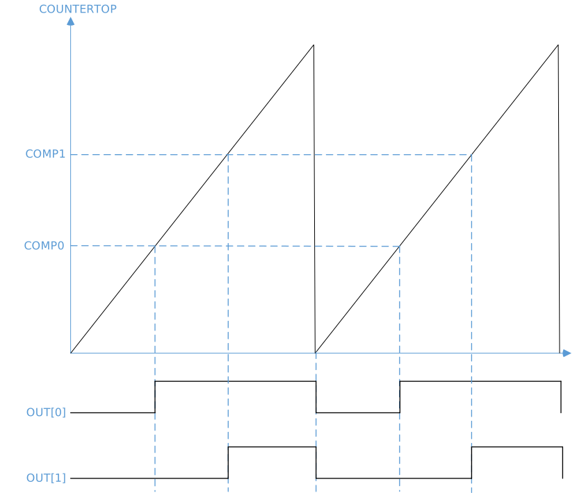
In up counting mode, the following formula can be used to compute PWM period and step size:
PWM period: TPWM(Up)= TPWM_CLK * COUNTERTOP
Step width/Resolution: Tsteps= TPWM_CLK
Figure 3 shows the counter operating in up and down mode with (MODE=PWM_MODE_UpAndDown) two PWM channels with the same frequency but different duty cycle and output polarity. The counter starts decrementing to zero when COUNTERTOP is reached and will invert the OUT[n] when compare value is hit for the second time. This results in a set of pulses that are center- aligned.
uint16_t pwm_seq[4] = {PWM_CH0_DUTY, PWM_CH1_DUTY, PWM_CH2_DUTY, PWM_CH3_DUTY};
NRF_PWM0->PSEL.OUT[0] = (first_pin << PWM_PSEL_OUT_PIN_Pos) |
                        (PWM_PSEL_OUT_CONNECT_Connected <<
                                                 PWM_PSEL_OUT_CONNECT_Pos);
NRF_PWM0->PSEL.OUT[1] = (second_pin << PWM_PSEL_OUT_PIN_Pos) |
                        (PWM_PSEL_OUT_CONNECT_Connected <<
                                                 PWM_PSEL_OUT_CONNECT_Pos);
NRF_PWM0->ENABLE      = (PWM_ENABLE_ENABLE_Enabled << PWM_ENABLE_ENABLE_Pos);
NRF_PWM0->MODE        = (PWM_MODE_UPDOWN_UpAndDown << PWM_MODE_UPDOWN_Pos);
NRF_PWM0->PRESCALER   = (PWM_PRESCALER_PRESCALER_DIV_1 <<
                                                 PWM_PRESCALER_PRESCALER_Pos);
NRF_PWM0->COUNTERTOP  = (16000 << PWM_COUNTERTOP_COUNTERTOP_Pos); //1 msec
NRF_PWM0->LOOP        = (PWM_LOOP_CNT_Disabled << PWM_LOOP_CNT_Pos);
NRF_PWM0->DECODER   = (PWM_DECODER_LOAD_Individual << PWM_DECODER_LOAD_Pos) |
                      (PWM_DECODER_MODE_RefreshCount << PWM_DECODER_MODE_Pos);
NRF_PWM0->SEQ[0].PTR  = ((uint32_t)(pwm_seq) << PWM_SEQ_PTR_PTR_Pos);
NRF_PWM0->SEQ[0].CNT  = ((sizeof(pwm_seq) / sizeof(uint16_t)) <<
                                                 PWM_SEQ_CNT_CNT_Pos);
NRF_PWM0->SEQ[0].REFRESH  = 0;
NRF_PWM0->SEQ[0].ENDDELAY = 0;
NRF_PWM0->TASKS_SEQSTART[0] = 1;
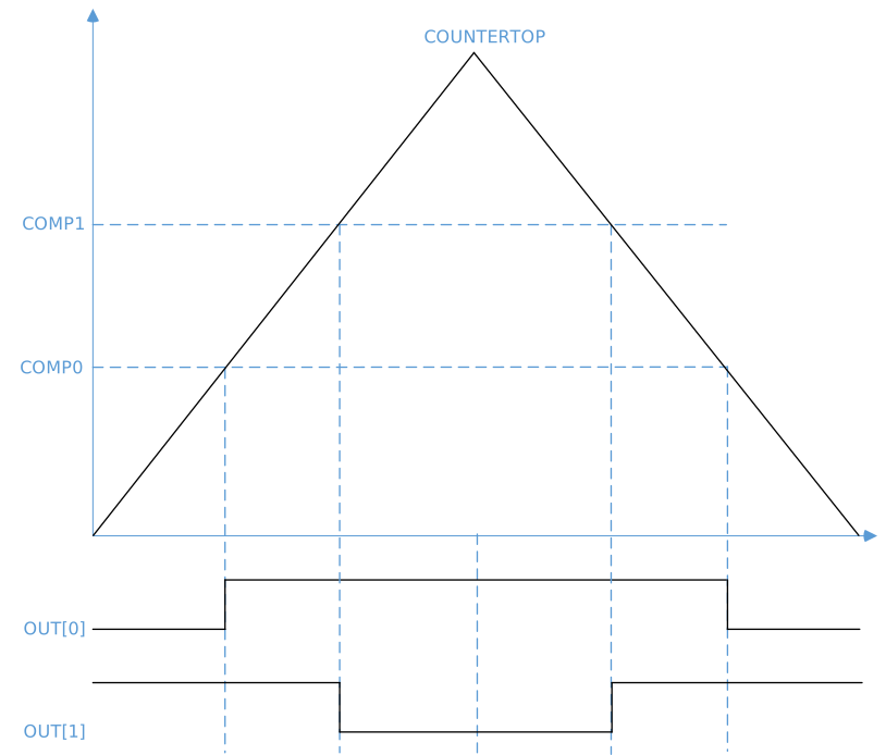
In up-and-down counting modes, the following formula can be used to compute PWM period and step size: TPWM(Up And Down) = TPWM_CLK * 2 * COUNTERTOP
Step width/Resolution: Tsteps = TPWM_CLK * 2
Decoder with EasyDMA
The decoder uses EasyDMA to take PWM parameters stored in Data RAM by ways of EasyDMA and updates the internal compare registers of the wave counter based on the mode of operation.
The mentioned PWM parameters are organized into a sequence containing at least one half word (16 bit). Its most significant bit[15] denotes the polarity of the OUT[n] while bit[14:0] is the 15-bit compare value. See below for further details of these RAM defined registers.
| Bit number | 31 | 30 | 29 | 28 | 27 | 26 | 25 | 24 | 23 | 22 | 21 | 20 | 19 | 18 | 17 | 16 | 15 | 14 | 13 | 12 | 11 | 10 | 9 | 8 | 7 | 6 | 5 | 4 | 3 | 2 | 1 | 0 | |||
|---|---|---|---|---|---|---|---|---|---|---|---|---|---|---|---|---|---|---|---|---|---|---|---|---|---|---|---|---|---|---|---|---|---|---|---|
| Id | B | A | A | A | A | A | A | A | A | A | A | A | A | A | A | A | |||||||||||||||||||
| Reset 0x00000000 | 0 | 0 | 0 | 0 | 0 | 0 | 0 | 0 | 0 | 0 | 0 | 0 | 0 | 0 | 0 | 0 | 0 | 0 | 0 | 0 | 0 | 0 | 0 | 0 | 0 | 0 | 0 | 0 | 0 | 0 | 0 | 0 | |||
| Id | RW | Field | Value Id | Value | Description | ||||||||||||||||||||||||||||||
| A | RW | COMPARE | Duty cycle setting - value loaded to internal compare register | ||||||||||||||||||||||||||||||||
| B | RW | POLARITY | Edge polarity of GPIO. | ||||||||||||||||||||||||||||||||
RisingEdge | 0 | First edge within the PWM period is rising | |||||||||||||||||||||||||||||||||
FallingEdge | 1 | First edge within the PWM period is falling | |||||||||||||||||||||||||||||||||
The DECODER register controls how the RAM content is interpreted and loaded to the internal compare registers. The LOAD field can be used to control if the RAM values are loaded to all compare channels - or alternatively to update a group or all channels with individual values. Figure 4 illustrates how the parameters stored in RAM are organized and routed to the various compare channels in the different modes.
A special mode of operation is available when DECODER.LOAD is set to WaveForm. In this mode, up to three PWM channels can be enabled - OUT[0] to OUT[2]. In RAM, four values are loaded at a time: the first, second and third location are used to load the values, and the fourth RAM location is used to load the COUNTERTOP register. This way one can have up to three PWM channels with a frequency base that changes on a per PWM period basis. This mode of operation is useful for arbitrary wave form generation in applications such as LED lighting.
The register SEQ[n].REFRESH=N (one per sequence n=0 or 1) will instruct a new RAM stored pulse width value on every (N+1)th PWM period. Setting the register to zero will result in a new duty cycle update every PWM period as long as the minimum PWM period is observed.
Note that registers SEQ[n].REFRESH and SEQ[n].ENDDELAY are ignored when DECODER.MODE=NextStep . The next value is loaded upon receiving every NEXTSTEP task.
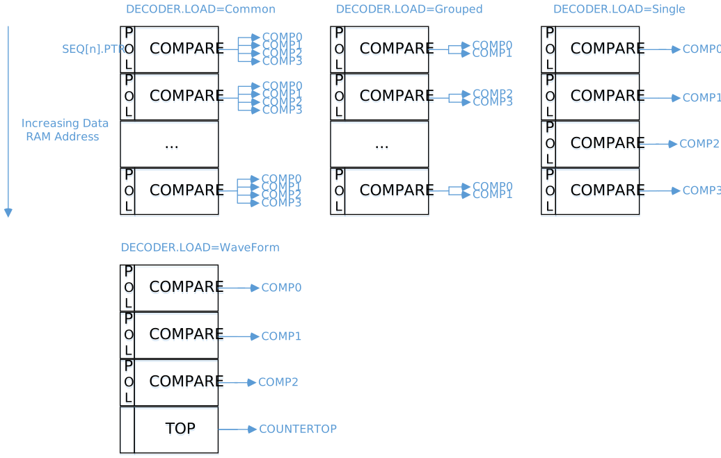
SEQ[n].PTR is the pointer used to fetch COMPARE values from RAM. If the SEQ[n].PTR is not pointing to the Data RAM region, an EasyDMA transfer may result in a HardFault or RAM corruption. See Memory for more information about the different memory regions.
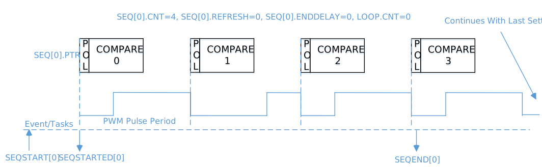
After the SEQ[n].PTR is set to the desired RAM location, the SEQ[n].CNT register must be set to the number of 16-bit half words in the sequence. It is important to observe that the Grouped and Single modes require one half word per group or one half word per channel respectively, and thus increases RAM size occupation. If PWM generation was not running yet at that point, sending the SEQSTART[n] task will load the first value from RAM, then start the PWM generation. A SEQSTARTED[n] event is generated as soon as the EasyDMA has read the first PWM parameter from RAM and the wave counter has started executing it. When LOOP.CNT=0, sequence n=0 or 1 is played back once. After the last value in the sequence has been loaded and started executing, a SEQEND[n] event is generated. The PWM generation will then continue with the last loaded value. See Figure 5 for an example of such simple playback.
To completely stop the PWM generation and force the associated pins to a defined state, a STOP task can be fired at any time. A STOPPED event is generated when the PWM generation has stopped at the end of currently running PWM period, and the pins go into their idle state as defined in GPIO->OUT. PWM generation can then only be restarted through a SEQSTART[n] task. SEQSTART[n] will resume PWM generation after having loaded the first value from the RAM buffer defined in the SEQ[n].PTR register.
The table below provides indication of when specific registers get sampled by the hardware. Care should be taken when updating these registers to avoid values to be applied earlier than expected.
| Register | Taken into account by hardware | Recommended (safe) update |
|---|---|---|
| SEQ[n].PTR | When sending the SEQSTART[n] task | After having received the SEQSTARTED[n] event |
| SEQ[n].CNT | When sending the SEQSTART[n] task | After having received the SEQSTARTED[n] event |
| SEQ[0].ENDDELAY | When sending the SEQSTART[0] task Every time a new value from sequence [0] has been loaded from RAM and gets applied to the Wave Counter (indicated by the PWMPERIODEND event) | Before starting sequence [0] through a SEQSTART[0] task When no more value from sequence [0] gets loaded from RAM (indicated by the SEQEND[0] event) At any time during sequence [1] (which starts when the SEQSTARTED[1] event is fired) |
| SEQ[1].ENDDELAY | When sending the SEQSTART[1] task Every time a new value from sequence [1] has been loaded from RAM and gets applied to the Wave Counter (indicated by the PWMPERIODEND event) | Before starting sequence [1] through a SEQSTART[1] task When no more value from sequence [1] gets loaded from RAM (indicated by the SEQEND[1] event) At any time during sequence [0] (which starts when the SEQSTARTED[0] event is fired) |
| SEQ[0].REFRESH | When sending the SEQSTART[0] task Every time a new value from sequence [0] has been loaded from RAM and gets applied to the Wave Counter (indicated by the PWMPERIODEND event) | Before starting sequence [0] through a SEQSTART[0] task At any time during sequence [1] (which starts when the SEQSTARTED[1] event is fired) |
| SEQ[1].REFRESH | When sending the SEQSTART[1] task Every time a new value from sequence [1] has been loaded from RAM and gets applied to the Wave Counter (indicated by the PWMPERIODEND event) | Before starting sequence [1] through a SEQSTART[1] task At any time during sequence [0] (which starts when the SEQSTARTED[0] event is fired) |
| COUNTERTOP | In DECODER.LOAD=WaveForm: this register is ignored. In all other LOAD modes: at the end of current PWM period (indicated by the PWMPERIODEND event) | Before starting PWM generation through a SEQSTART[n] task After a STOP task has been issued, and the STOPPED event has been received. |
| MODE | Immediately | Before starting PWM generation through a SEQSTART[n] task After a STOP task has been issued, and the STOPPED event has been received. |
| DECODER | Immediately | Before starting PWM generation through a SEQSTART[n] task After a STOP task has been issued, and the STOPPED event has been received. |
| PRESCALER | Immediately | Before starting PWM generation through a SEQSTART[n] task After a STOP task has been issued, and the STOPPED event has been received. |
| LOOP | Immediately | Before starting PWM generation through a SEQSTART[n] task After a STOP task has been issued, and the STOPPED event has been received. |
| PSEL.OUT[n] | Immediately | Before enabling the PWM instance through the ENABLE register |
NRF_PWM0->PSEL.OUT[0] = (first_pin << PWM_PSEL_OUT_PIN_Pos) |
                        (PWM_PSEL_OUT_CONNECT_Connected <<
                                                 PWM_PSEL_OUT_CONNECT_Pos);
NRF_PWM0->ENABLE      = (PWM_ENABLE_ENABLE_Enabled << PWM_ENABLE_ENABLE_Pos);
NRF_PWM0->MODE        = (PWM_MODE_UPDOWN_Up << PWM_MODE_UPDOWN_Pos);
NRF_PWM0->PRESCALER   = (PWM_PRESCALER_PRESCALER_DIV_1 <<
                                                 PWM_PRESCALER_PRESCALER_Pos);
NRF_PWM0->COUNTERTOP  = (16000 << PWM_COUNTERTOP_COUNTERTOP_Pos); //1 msec
NRF_PWM0->LOOP        = (PWM_LOOP_CNT_Disabled << PWM_LOOP_CNT_Pos);
NRF_PWM0->DECODER   = (PWM_DECODER_LOAD_Common << PWM_DECODER_LOAD_Pos) |
                      (PWM_DECODER_MODE_RefreshCount << PWM_DECODER_MODE_Pos);
NRF_PWM0->SEQ[0].PTR  = ((uint32_t)(seq0_ram) << PWM_SEQ_PTR_PTR_Pos);
NRF_PWM0->SEQ[0].CNT  = ((sizeof(seq0_ram) / sizeof(uint16_t)) <<
                                                 PWM_SEQ_CNT_CNT_Pos);
NRF_PWM0->SEQ[0].REFRESH  = 0;
NRF_PWM0->SEQ[0].ENDDELAY = 0;
NRF_PWM0->TASKS_SEQSTART[0] = 1;
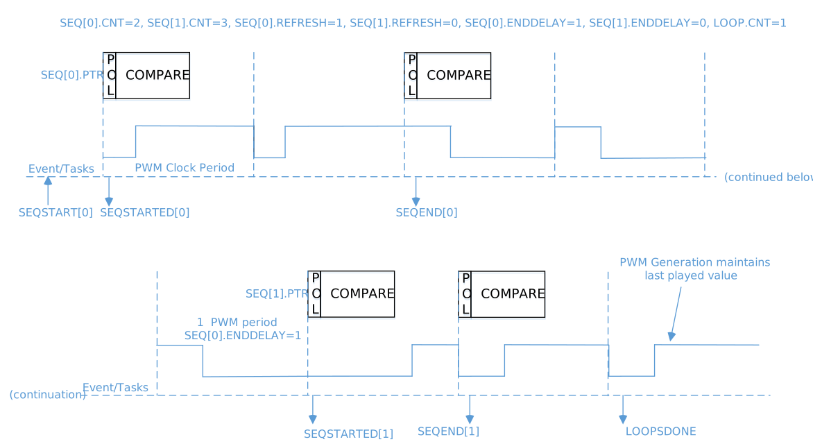
A more complex example is shown in Figure 6, where LOOP.CNT>0 . In this case, an automated playback takes place, consisting of SEQ[0], delay 0, SEQ[1], delay 1, then again SEQ[0], etc. The user can choose to start a complex playback with SEQ[0] or SEQ[1] through sending the SEQSTART[0] or SEQSTART[1] task.
The complex playback always ends with delay 1.
The two sequences 0 and 1 are defined with address of values tables in Data RAM (pointed by SEQ[n].PTR) and respective buffer size (SEQ[n].CNT). The rate at which a new value is loaded is defined individually for each sequence by SEQ[n].REFRESH . The chaining of sequence 1 following sequence 0 is implicit, the LOOP.CNT register allows the chaining of sequence 1 to sequence 0 for a determined number of times. In other words, it allows to repeat a complex sequence a number of times in a fully automated way.
NRF_PWM0->PSEL.OUT[0] = (first_pin << PWM_PSEL_OUT_PIN_Pos) |
                        (PWM_PSEL_OUT_CONNECT_Connected <<
                                                 PWM_PSEL_OUT_CONNECT_Pos);
NRF_PWM0->ENABLE      = (PWM_ENABLE_ENABLE_Enabled << PWM_ENABLE_ENABLE_Pos);
NRF_PWM0->MODE        = (PWM_MODE_UPDOWN_Up << PWM_MODE_UPDOWN_Pos);
NRF_PWM0->PRESCALER   = (PWM_PRESCALER_PRESCALER_DIV_1 <<
                                                 PWM_PRESCALER_PRESCALER_Pos);
NRF_PWM0->COUNTERTOP  = (16000 << PWM_COUNTERTOP_COUNTERTOP_Pos); //1 msec
NRF_PWM0->LOOP        = (1 << PWM_LOOP_CNT_Pos);
NRF_PWM0->DECODER   = (PWM_DECODER_LOAD_Common << PWM_DECODER_LOAD_Pos) |
                      (PWM_DECODER_MODE_RefreshCount << PWM_DECODER_MODE_Pos);
NRF_PWM0->SEQ[0].PTR  = ((uint32_t)(seq0_ram) << PWM_SEQ_PTR_PTR_Pos);
NRF_PWM0->SEQ[0].CNT  = ((sizeof(seq0_ram) / sizeof(uint16_t)) <<
                                                 PWM_SEQ_CNT_CNT_Pos);
NRF_PWM0->SEQ[0].REFRESH  = 1;
NRF_PWM0->SEQ[0].ENDDELAY = 1;
NRF_PWM0->SEQ[1].PTR  = ((uint32_t)(seq1_ram) << PWM_SEQ_PTR_PTR_Pos);
NRF_PWM0->SEQ[1].CNT  = ((sizeof(seq1_ram) / sizeof(uint16_t)) <<
                                                 PWM_SEQ_CNT_CNT_Pos);
NRF_PWM0->SEQ[1].REFRESH  = 0;
NRF_PWM0->SEQ[1].ENDDELAY = 0;
NRF_PWM0->TASKS_SEQSTART[0] = 1;
The decoder can also be configured to asynchronously load a new PWM duty cycle. If the DECODER.MODE register is set to NextStep - then the NEXTSTEP task will cause an update of the internal compare registers on the next PWM period.
- Initial and final duty cycle on the PWM output(s)
- Chaining of SEQ[0] and SEQ[1] if LOOP.CNT>0
- Influence of registers on the sequence
- Events fired during a sequence
- DMA activity (loading of next value and applying it to the output(s))
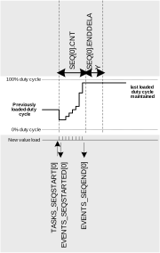
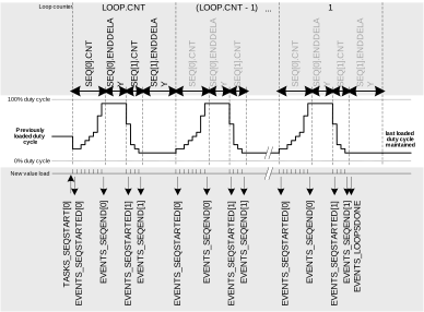
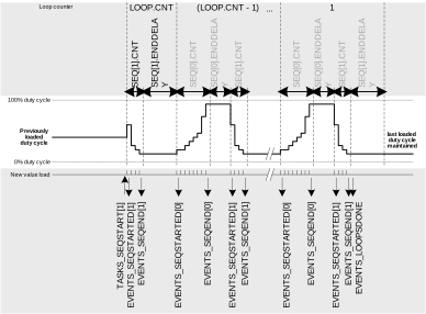
Note that if a sequence is in use in a simple or complex sequence, it must have a length of SEQ[n].CNT > 0 .
Limitations
The previous compare value will be repeated if the PWM period is selected to be shorter than the time it takes for the EasyDMA to fetch from RAM and update the internal compare registers.
This is to ensure a glitch-free operation even if very short PWM periods are chosen.
Pin configuration
The OUT[n] (n=0..3) signals associated to each channel of the PWM module are mapped to physical pins according to the configuration specified in the respective PSEL.OUT[n] registers. If a PSEL.OUT[n].CONNECT is set to Disconnected, the associated PWM module signal will not be connected to any physical pins.
The PSEL.OUT[n] registers and their configurations are only used as long as the PWM module is enabled and PWM generation is active (wave counter started), and retained only as long as the device is in System ON mode, see POWER chapter for more information about power modes.
To ensure correct behaviour in the PWM module, the pins used by the PWM module must be configured in the GPIO peripheral as described in Table 2 before enabling the PWM module. The pins' idle state is defined by the OUT registers in the GPIO module. This is to ensure that the pins used by the PWM module are driven correctly, if PWM generation is stopped through a STOP task, the PWM module itself is temporarily disabled, or the device temporarily enters System OFF. This configuration must be retained in the GPIO for the selected IOs as long as the PWM module is supposed to be connected to an external PWM circuit.
Only one peripheral can be assigned to drive a particular GPIO pin at a time. Failing to do so may result in unpredictable behaviour.
| PWM signal | PWM pin | Direction | Output value | Comment |
|---|---|---|---|---|
| OUT[n] | As specified in PSEL.OUT[n] (n=0..3) | Output | 0 | Idle state defined in GPIO->OUT |
Registers
| Base address | Peripheral | Instance | Description | Configuration | |
|---|---|---|---|---|---|
| 0x4001C000 | PWM | PWM0 | Pulse Width Modulation Unit 0 | ||
| 0x40021000 | PWM | PWM1 | Pulse Width Modulation Unit 1 | ||
| 0x40022000 | PWM | PWM2 | Pulse Width Modulation Unit 2 | ||
| Register | Offset | Description | |
|---|---|---|---|
| TASKS_STOP | 0x004 | Stops PWM pulse generation on all channels at the end of current PWM period, and stops sequence playback | |
| TASKS_SEQSTART[0] | 0x008 | Loads the first PWM value on all enabled channels from sequence 0, and starts playing that sequence at the rate defined in SEQ[0]REFRESH and/or DECODER.MODE. Causes PWM generation to start it was not running. | |
| TASKS_SEQSTART[1] | 0x00C | Loads the first PWM value on all enabled channels from sequence 1, and starts playing that sequence at the rate defined in SEQ[1]REFRESH and/or DECODER.MODE. Causes PWM generation to start it was not running. | |
| TASKS_NEXTSTEP | 0x010 | Steps by one value in the current sequence on all enabled channels if DECODER.MODE=NextStep. Does not cause PWM generation to start it was not running. | |
| EVENTS_STOPPED | 0x104 | Response to STOP task, emitted when PWM pulses are no longer generated | |
| EVENTS_SEQSTARTED[0] | 0x108 | First PWM period started on sequence 0 | |
| EVENTS_SEQSTARTED[1] | 0x10C | First PWM period started on sequence 1 | |
| EVENTS_SEQEND[0] | 0x110 | Emitted at end of every sequence 0, when last value from RAM has been applied to wave counter | |
| EVENTS_SEQEND[1] | 0x114 | Emitted at end of every sequence 1, when last value from RAM has been applied to wave counter | |
| EVENTS_PWMPERIODEND | 0x118 | Emitted at the end of each PWM period | |
| EVENTS_LOOPSDONE | 0x11C | Concatenated sequences have been played the amount of times defined in LOOP.CNT | |
| SHORTS | 0x200 | Shortcut register | |
| INTEN | 0x300 | Enable or disable interrupt | |
| INTENSET | 0x304 | Enable interrupt | |
| INTENCLR | 0x308 | Disable interrupt | |
| ENABLE | 0x500 | PWM module enable register | |
| MODE | 0x504 | Selects operating mode of the wave counter | |
| COUNTERTOP | 0x508 | Value up to which the pulse generator counter counts | |
| PRESCALER | 0x50C | Configuration for PWM_CLK | |
| DECODER | 0x510 | Configuration of the decoder | |
| LOOP | 0x514 | Amount of playback of a loop | |
| SEQ[0].PTR | 0x520 | Beginning address in Data RAM of this sequence | |
| SEQ[0].CNT | 0x524 | Amount of values (duty cycles) in this sequence | |
| SEQ[0].REFRESH | 0x528 | Amount of additional PWM periods between samples loaded into compare register | |
| SEQ[0].ENDDELAY | 0x52C | Time added after the sequence | |
| SEQ[1].PTR | 0x540 | Beginning address in Data RAM of this sequence | |
| SEQ[1].CNT | 0x544 | Amount of values (duty cycles) in this sequence | |
| SEQ[1].REFRESH | 0x548 | Amount of additional PWM periods between samples loaded into compare register | |
| SEQ[1].ENDDELAY | 0x54C | Time added after the sequence | |
| PSEL.OUT[0] | 0x560 | Output pin select for PWM channel 0 | |
| PSEL.OUT[1] | 0x564 | Output pin select for PWM channel 1 | |
| PSEL.OUT[2] | 0x568 | Output pin select for PWM channel 2 | |
| PSEL.OUT[3] | 0x56C | Output pin select for PWM channel 3 | |
SHORTS
Address offset: 0x200
Shortcut register
| Bit number | 31 | 30 | 29 | 28 | 27 | 26 | 25 | 24 | 23 | 22 | 21 | 20 | 19 | 18 | 17 | 16 | 15 | 14 | 13 | 12 | 11 | 10 | 9 | 8 | 7 | 6 | 5 | 4 | 3 | 2 | 1 | 0 | |||
|---|---|---|---|---|---|---|---|---|---|---|---|---|---|---|---|---|---|---|---|---|---|---|---|---|---|---|---|---|---|---|---|---|---|---|---|
| Id | E | D | C | B | A | ||||||||||||||||||||||||||||||
| Reset 0x00000000 | 0 | 0 | 0 | 0 | 0 | 0 | 0 | 0 | 0 | 0 | 0 | 0 | 0 | 0 | 0 | 0 | 0 | 0 | 0 | 0 | 0 | 0 | 0 | 0 | 0 | 0 | 0 | 0 | 0 | 0 | 0 | 0 | |||
| Id | RW | Field | Value Id | Value | Description | ||||||||||||||||||||||||||||||
| A | RW | SEQEND0_STOP | Shortcut between SEQEND[0] event and STOP task See EVENTS_SEQEND[0] and TASKS_STOP | ||||||||||||||||||||||||||||||||
Disabled | 0 | Disable shortcut | |||||||||||||||||||||||||||||||||
Enabled | 1 | Enable shortcut | |||||||||||||||||||||||||||||||||
| B | RW | SEQEND1_STOP | Shortcut between SEQEND[1] event and STOP task See EVENTS_SEQEND[1] and TASKS_STOP | ||||||||||||||||||||||||||||||||
Disabled | 0 | Disable shortcut | |||||||||||||||||||||||||||||||||
Enabled | 1 | Enable shortcut | |||||||||||||||||||||||||||||||||
| C | RW | LOOPSDONE_SEQSTART0 | Shortcut between LOOPSDONE event and SEQSTART[0] task See EVENTS_LOOPSDONE and TASKS_SEQSTART[0] | ||||||||||||||||||||||||||||||||
Disabled | 0 | Disable shortcut | |||||||||||||||||||||||||||||||||
Enabled | 1 | Enable shortcut | |||||||||||||||||||||||||||||||||
| D | RW | LOOPSDONE_SEQSTART1 | Shortcut between LOOPSDONE event and SEQSTART[1] task See EVENTS_LOOPSDONE and TASKS_SEQSTART[1] | ||||||||||||||||||||||||||||||||
Disabled | 0 | Disable shortcut | |||||||||||||||||||||||||||||||||
Enabled | 1 | Enable shortcut | |||||||||||||||||||||||||||||||||
| E | RW | LOOPSDONE_STOP | Shortcut between LOOPSDONE event and STOP task See EVENTS_LOOPSDONE and TASKS_STOP | ||||||||||||||||||||||||||||||||
Disabled | 0 | Disable shortcut | |||||||||||||||||||||||||||||||||
Enabled | 1 | Enable shortcut | |||||||||||||||||||||||||||||||||
INTEN
Address offset: 0x300
Enable or disable interrupt
| Bit number | 31 | 30 | 29 | 28 | 27 | 26 | 25 | 24 | 23 | 22 | 21 | 20 | 19 | 18 | 17 | 16 | 15 | 14 | 13 | 12 | 11 | 10 | 9 | 8 | 7 | 6 | 5 | 4 | 3 | 2 | 1 | 0 | |||
|---|---|---|---|---|---|---|---|---|---|---|---|---|---|---|---|---|---|---|---|---|---|---|---|---|---|---|---|---|---|---|---|---|---|---|---|
| Id | H | G | F | E | D | C | B | ||||||||||||||||||||||||||||
| Reset 0x00000000 | 0 | 0 | 0 | 0 | 0 | 0 | 0 | 0 | 0 | 0 | 0 | 0 | 0 | 0 | 0 | 0 | 0 | 0 | 0 | 0 | 0 | 0 | 0 | 0 | 0 | 0 | 0 | 0 | 0 | 0 | 0 | 0 | |||
| Id | RW | Field | Value Id | Value | Description | ||||||||||||||||||||||||||||||
| B | RW | STOPPED | Enable or disable interrupt for STOPPED event See EVENTS_STOPPED | ||||||||||||||||||||||||||||||||
Disabled | 0 | Disable | |||||||||||||||||||||||||||||||||
Enabled | 1 | Enable | |||||||||||||||||||||||||||||||||
| C | RW | SEQSTARTED0 | Enable or disable interrupt for SEQSTARTED[0] event | ||||||||||||||||||||||||||||||||
Disabled | 0 | Disable | |||||||||||||||||||||||||||||||||
Enabled | 1 | Enable | |||||||||||||||||||||||||||||||||
| D | RW | SEQSTARTED1 | Enable or disable interrupt for SEQSTARTED[1] event | ||||||||||||||||||||||||||||||||
Disabled | 0 | Disable | |||||||||||||||||||||||||||||||||
Enabled | 1 | Enable | |||||||||||||||||||||||||||||||||
| E | RW | SEQEND0 | Enable or disable interrupt for SEQEND[0] event See EVENTS_SEQEND[0] | ||||||||||||||||||||||||||||||||
Disabled | 0 | Disable | |||||||||||||||||||||||||||||||||
Enabled | 1 | Enable | |||||||||||||||||||||||||||||||||
| F | RW | SEQEND1 | Enable or disable interrupt for SEQEND[1] event See EVENTS_SEQEND[1] | ||||||||||||||||||||||||||||||||
Disabled | 0 | Disable | |||||||||||||||||||||||||||||||||
Enabled | 1 | Enable | |||||||||||||||||||||||||||||||||
| G | RW | PWMPERIODEND | Enable or disable interrupt for PWMPERIODEND event | ||||||||||||||||||||||||||||||||
Disabled | 0 | Disable | |||||||||||||||||||||||||||||||||
Enabled | 1 | Enable | |||||||||||||||||||||||||||||||||
| H | RW | LOOPSDONE | Enable or disable interrupt for LOOPSDONE event See EVENTS_LOOPSDONE | ||||||||||||||||||||||||||||||||
Disabled | 0 | Disable | |||||||||||||||||||||||||||||||||
Enabled | 1 | Enable | |||||||||||||||||||||||||||||||||
INTENSET
Address offset: 0x304
Enable interrupt
| Bit number | 31 | 30 | 29 | 28 | 27 | 26 | 25 | 24 | 23 | 22 | 21 | 20 | 19 | 18 | 17 | 16 | 15 | 14 | 13 | 12 | 11 | 10 | 9 | 8 | 7 | 6 | 5 | 4 | 3 | 2 | 1 | 0 | |||
|---|---|---|---|---|---|---|---|---|---|---|---|---|---|---|---|---|---|---|---|---|---|---|---|---|---|---|---|---|---|---|---|---|---|---|---|
| Id | H | G | F | E | D | C | B | ||||||||||||||||||||||||||||
| Reset 0x00000000 | 0 | 0 | 0 | 0 | 0 | 0 | 0 | 0 | 0 | 0 | 0 | 0 | 0 | 0 | 0 | 0 | 0 | 0 | 0 | 0 | 0 | 0 | 0 | 0 | 0 | 0 | 0 | 0 | 0 | 0 | 0 | 0 | |||
| Id | RW | Field | Value Id | Value | Description | ||||||||||||||||||||||||||||||
| B | RW | STOPPED | Write '1' to Enable interrupt for STOPPED event See EVENTS_STOPPED | ||||||||||||||||||||||||||||||||
Set | 1 | Enable | |||||||||||||||||||||||||||||||||
Disabled | 0 | Read: Disabled | |||||||||||||||||||||||||||||||||
Enabled | 1 | Read: Enabled | |||||||||||||||||||||||||||||||||
| C | RW | SEQSTARTED0 | Write '1' to Enable interrupt for SEQSTARTED[0] event | ||||||||||||||||||||||||||||||||
Set | 1 | Enable | |||||||||||||||||||||||||||||||||
Disabled | 0 | Read: Disabled | |||||||||||||||||||||||||||||||||
Enabled | 1 | Read: Enabled | |||||||||||||||||||||||||||||||||
| D | RW | SEQSTARTED1 | Write '1' to Enable interrupt for SEQSTARTED[1] event | ||||||||||||||||||||||||||||||||
Set | 1 | Enable | |||||||||||||||||||||||||||||||||
Disabled | 0 | Read: Disabled | |||||||||||||||||||||||||||||||||
Enabled | 1 | Read: Enabled | |||||||||||||||||||||||||||||||||
| E | RW | SEQEND0 | Write '1' to Enable interrupt for SEQEND[0] event See EVENTS_SEQEND[0] | ||||||||||||||||||||||||||||||||
Set | 1 | Enable | |||||||||||||||||||||||||||||||||
Disabled | 0 | Read: Disabled | |||||||||||||||||||||||||||||||||
Enabled | 1 | Read: Enabled | |||||||||||||||||||||||||||||||||
| F | RW | SEQEND1 | Write '1' to Enable interrupt for SEQEND[1] event See EVENTS_SEQEND[1] | ||||||||||||||||||||||||||||||||
Set | 1 | Enable | |||||||||||||||||||||||||||||||||
Disabled | 0 | Read: Disabled | |||||||||||||||||||||||||||||||||
Enabled | 1 | Read: Enabled | |||||||||||||||||||||||||||||||||
| G | RW | PWMPERIODEND | Write '1' to Enable interrupt for PWMPERIODEND event | ||||||||||||||||||||||||||||||||
Set | 1 | Enable | |||||||||||||||||||||||||||||||||
Disabled | 0 | Read: Disabled | |||||||||||||||||||||||||||||||||
Enabled | 1 | Read: Enabled | |||||||||||||||||||||||||||||||||
| H | RW | LOOPSDONE | Write '1' to Enable interrupt for LOOPSDONE event See EVENTS_LOOPSDONE | ||||||||||||||||||||||||||||||||
Set | 1 | Enable | |||||||||||||||||||||||||||||||||
Disabled | 0 | Read: Disabled | |||||||||||||||||||||||||||||||||
Enabled | 1 | Read: Enabled | |||||||||||||||||||||||||||||||||
INTENCLR
Address offset: 0x308
Disable interrupt
| Bit number | 31 | 30 | 29 | 28 | 27 | 26 | 25 | 24 | 23 | 22 | 21 | 20 | 19 | 18 | 17 | 16 | 15 | 14 | 13 | 12 | 11 | 10 | 9 | 8 | 7 | 6 | 5 | 4 | 3 | 2 | 1 | 0 | |||
|---|---|---|---|---|---|---|---|---|---|---|---|---|---|---|---|---|---|---|---|---|---|---|---|---|---|---|---|---|---|---|---|---|---|---|---|
| Id | H | G | F | E | D | C | B | ||||||||||||||||||||||||||||
| Reset 0x00000000 | 0 | 0 | 0 | 0 | 0 | 0 | 0 | 0 | 0 | 0 | 0 | 0 | 0 | 0 | 0 | 0 | 0 | 0 | 0 | 0 | 0 | 0 | 0 | 0 | 0 | 0 | 0 | 0 | 0 | 0 | 0 | 0 | |||
| Id | RW | Field | Value Id | Value | Description | ||||||||||||||||||||||||||||||
| B | RW | STOPPED | Write '1' to Disable interrupt for STOPPED event See EVENTS_STOPPED | ||||||||||||||||||||||||||||||||
Clear | 1 | Disable | |||||||||||||||||||||||||||||||||
Disabled | 0 | Read: Disabled | |||||||||||||||||||||||||||||||||
Enabled | 1 | Read: Enabled | |||||||||||||||||||||||||||||||||
| C | RW | SEQSTARTED0 | Write '1' to Disable interrupt for SEQSTARTED[0] event | ||||||||||||||||||||||||||||||||
Clear | 1 | Disable | |||||||||||||||||||||||||||||||||
Disabled | 0 | Read: Disabled | |||||||||||||||||||||||||||||||||
Enabled | 1 | Read: Enabled | |||||||||||||||||||||||||||||||||
| D | RW | SEQSTARTED1 | Write '1' to Disable interrupt for SEQSTARTED[1] event | ||||||||||||||||||||||||||||||||
Clear | 1 | Disable | |||||||||||||||||||||||||||||||||
Disabled | 0 | Read: Disabled | |||||||||||||||||||||||||||||||||
Enabled | 1 | Read: Enabled | |||||||||||||||||||||||||||||||||
| E | RW | SEQEND0 | Write '1' to Disable interrupt for SEQEND[0] event See EVENTS_SEQEND[0] | ||||||||||||||||||||||||||||||||
Clear | 1 | Disable | |||||||||||||||||||||||||||||||||
Disabled | 0 | Read: Disabled | |||||||||||||||||||||||||||||||||
Enabled | 1 | Read: Enabled | |||||||||||||||||||||||||||||||||
| F | RW | SEQEND1 | Write '1' to Disable interrupt for SEQEND[1] event See EVENTS_SEQEND[1] | ||||||||||||||||||||||||||||||||
Clear | 1 | Disable | |||||||||||||||||||||||||||||||||
Disabled | 0 | Read: Disabled | |||||||||||||||||||||||||||||||||
Enabled | 1 | Read: Enabled | |||||||||||||||||||||||||||||||||
| G | RW | PWMPERIODEND | Write '1' to Disable interrupt for PWMPERIODEND event | ||||||||||||||||||||||||||||||||
Clear | 1 | Disable | |||||||||||||||||||||||||||||||||
Disabled | 0 | Read: Disabled | |||||||||||||||||||||||||||||||||
Enabled | 1 | Read: Enabled | |||||||||||||||||||||||||||||||||
| H | RW | LOOPSDONE | Write '1' to Disable interrupt for LOOPSDONE event See EVENTS_LOOPSDONE | ||||||||||||||||||||||||||||||||
Clear | 1 | Disable | |||||||||||||||||||||||||||||||||
Disabled | 0 | Read: Disabled | |||||||||||||||||||||||||||||||||
Enabled | 1 | Read: Enabled | |||||||||||||||||||||||||||||||||
ENABLE
Address offset: 0x500
PWM module enable register
| Bit number | 31 | 30 | 29 | 28 | 27 | 26 | 25 | 24 | 23 | 22 | 21 | 20 | 19 | 18 | 17 | 16 | 15 | 14 | 13 | 12 | 11 | 10 | 9 | 8 | 7 | 6 | 5 | 4 | 3 | 2 | 1 | 0 | |||
|---|---|---|---|---|---|---|---|---|---|---|---|---|---|---|---|---|---|---|---|---|---|---|---|---|---|---|---|---|---|---|---|---|---|---|---|
| Id | A | ||||||||||||||||||||||||||||||||||
| Reset 0x00000000 | 0 | 0 | 0 | 0 | 0 | 0 | 0 | 0 | 0 | 0 | 0 | 0 | 0 | 0 | 0 | 0 | 0 | 0 | 0 | 0 | 0 | 0 | 0 | 0 | 0 | 0 | 0 | 0 | 0 | 0 | 0 | 0 | |||
| Id | RW | Field | Value Id | Value | Description | ||||||||||||||||||||||||||||||
| A | RW | ENABLE | Enable or disable PWM module | ||||||||||||||||||||||||||||||||
Disabled | 0 | Disabled | |||||||||||||||||||||||||||||||||
Enabled | 1 | Enable | |||||||||||||||||||||||||||||||||
MODE
Address offset: 0x504
Selects operating mode of the wave counter
| Bit number | 31 | 30 | 29 | 28 | 27 | 26 | 25 | 24 | 23 | 22 | 21 | 20 | 19 | 18 | 17 | 16 | 15 | 14 | 13 | 12 | 11 | 10 | 9 | 8 | 7 | 6 | 5 | 4 | 3 | 2 | 1 | 0 | |||
|---|---|---|---|---|---|---|---|---|---|---|---|---|---|---|---|---|---|---|---|---|---|---|---|---|---|---|---|---|---|---|---|---|---|---|---|
| Id | A | ||||||||||||||||||||||||||||||||||
| Reset 0x00000000 | 0 | 0 | 0 | 0 | 0 | 0 | 0 | 0 | 0 | 0 | 0 | 0 | 0 | 0 | 0 | 0 | 0 | 0 | 0 | 0 | 0 | 0 | 0 | 0 | 0 | 0 | 0 | 0 | 0 | 0 | 0 | 0 | |||
| Id | RW | Field | Value Id | Value | Description | ||||||||||||||||||||||||||||||
| A | RW | UPDOWN | Selects up or up and down as wave counter mode | ||||||||||||||||||||||||||||||||
Up | 0 | Up counter - edge aligned PWM duty-cycle | |||||||||||||||||||||||||||||||||
UpAndDown | 1 | Up and down counter - center aligned PWM duty cycle | |||||||||||||||||||||||||||||||||
COUNTERTOP
Address offset: 0x508
Value up to which the pulse generator counter counts
| Bit number | 31 | 30 | 29 | 28 | 27 | 26 | 25 | 24 | 23 | 22 | 21 | 20 | 19 | 18 | 17 | 16 | 15 | 14 | 13 | 12 | 11 | 10 | 9 | 8 | 7 | 6 | 5 | 4 | 3 | 2 | 1 | 0 | |||
|---|---|---|---|---|---|---|---|---|---|---|---|---|---|---|---|---|---|---|---|---|---|---|---|---|---|---|---|---|---|---|---|---|---|---|---|
| Id | A | A | A | A | A | A | A | A | A | A | A | A | A | A | A | ||||||||||||||||||||
| Reset 0x000003FF | 0 | 0 | 0 | 0 | 0 | 0 | 0 | 0 | 0 | 0 | 0 | 0 | 0 | 0 | 0 | 0 | 0 | 0 | 0 | 0 | 0 | 0 | 1 | 1 | 1 | 1 | 1 | 1 | 1 | 1 | 1 | 1 | |||
| Id | RW | Field | Value Id | Value | Description | ||||||||||||||||||||||||||||||
| A | RW | COUNTERTOP | [3..32767] | Value up to which the pulse generator counter counts. This register is ignored when DECODER.MODE=WaveForm and only values from RAM will be used. | |||||||||||||||||||||||||||||||
PRESCALER
Address offset: 0x50C
Configuration for PWM_CLK
| Bit number | 31 | 30 | 29 | 28 | 27 | 26 | 25 | 24 | 23 | 22 | 21 | 20 | 19 | 18 | 17 | 16 | 15 | 14 | 13 | 12 | 11 | 10 | 9 | 8 | 7 | 6 | 5 | 4 | 3 | 2 | 1 | 0 | |||
|---|---|---|---|---|---|---|---|---|---|---|---|---|---|---|---|---|---|---|---|---|---|---|---|---|---|---|---|---|---|---|---|---|---|---|---|
| Id | A | A | A | ||||||||||||||||||||||||||||||||
| Reset 0x00000000 | 0 | 0 | 0 | 0 | 0 | 0 | 0 | 0 | 0 | 0 | 0 | 0 | 0 | 0 | 0 | 0 | 0 | 0 | 0 | 0 | 0 | 0 | 0 | 0 | 0 | 0 | 0 | 0 | 0 | 0 | 0 | 0 | |||
| Id | RW | Field | Value Id | Value | Description | ||||||||||||||||||||||||||||||
| A | RW | PRESCALER | Pre-scaler of PWM_CLK | ||||||||||||||||||||||||||||||||
DIV_1 | 0 | Divide by 1 (16MHz) | |||||||||||||||||||||||||||||||||
DIV_2 | 1 | Divide by 2 ( 8MHz) | |||||||||||||||||||||||||||||||||
DIV_4 | 2 | Divide by 4 ( 4MHz) | |||||||||||||||||||||||||||||||||
DIV_8 | 3 | Divide by 8 ( 2MHz) | |||||||||||||||||||||||||||||||||
DIV_16 | 4 | Divide by 16 ( 1MHz) | |||||||||||||||||||||||||||||||||
DIV_32 | 5 | Divide by 32 ( 500kHz) | |||||||||||||||||||||||||||||||||
DIV_64 | 6 | Divide by 64 ( 250kHz) | |||||||||||||||||||||||||||||||||
DIV_128 | 7 | Divide by 128 ( 125kHz) | |||||||||||||||||||||||||||||||||
DECODER
Address offset: 0x510
Configuration of the decoder
| Bit number | 31 | 30 | 29 | 28 | 27 | 26 | 25 | 24 | 23 | 22 | 21 | 20 | 19 | 18 | 17 | 16 | 15 | 14 | 13 | 12 | 11 | 10 | 9 | 8 | 7 | 6 | 5 | 4 | 3 | 2 | 1 | 0 | |||
|---|---|---|---|---|---|---|---|---|---|---|---|---|---|---|---|---|---|---|---|---|---|---|---|---|---|---|---|---|---|---|---|---|---|---|---|
| Id | B | A | A | ||||||||||||||||||||||||||||||||
| Reset 0x00000000 | 0 | 0 | 0 | 0 | 0 | 0 | 0 | 0 | 0 | 0 | 0 | 0 | 0 | 0 | 0 | 0 | 0 | 0 | 0 | 0 | 0 | 0 | 0 | 0 | 0 | 0 | 0 | 0 | 0 | 0 | 0 | 0 | |||
| Id | RW | Field | Value Id | Value | Description | ||||||||||||||||||||||||||||||
| A | RW | LOAD | How a sequence is read from RAM and spread to the compare register | ||||||||||||||||||||||||||||||||
Common | 0 | 1st half word (16-bit) used in all PWM channels 0..3 | |||||||||||||||||||||||||||||||||
Grouped | 1 | 1st half word (16-bit) used in channel 0..1; 2nd word in channel 2..3 | |||||||||||||||||||||||||||||||||
Individual | 2 | 1st half word (16-bit) in ch.0; 2nd in ch.1; ...; 4th in ch.3 | |||||||||||||||||||||||||||||||||
WaveForm | 3 | 1st half word (16-bit) in ch.0; 2nd in ch.1; ...; 4th in COUNTERTOP | |||||||||||||||||||||||||||||||||
| B | RW | MODE | Selects source for advancing the active sequence | ||||||||||||||||||||||||||||||||
RefreshCount | 0 | SEQ[n].REFRESH is used to determine loading internal compare registers | |||||||||||||||||||||||||||||||||
NextStep | 1 | NEXTSTEP task causes a new value to be loaded to internal compare registers | |||||||||||||||||||||||||||||||||
LOOP
Address offset: 0x514
Amount of playback of a loop
| Bit number | 31 | 30 | 29 | 28 | 27 | 26 | 25 | 24 | 23 | 22 | 21 | 20 | 19 | 18 | 17 | 16 | 15 | 14 | 13 | 12 | 11 | 10 | 9 | 8 | 7 | 6 | 5 | 4 | 3 | 2 | 1 | 0 | |||
|---|---|---|---|---|---|---|---|---|---|---|---|---|---|---|---|---|---|---|---|---|---|---|---|---|---|---|---|---|---|---|---|---|---|---|---|
| Id | A | A | A | A | A | A | A | A | A | A | A | A | A | A | A | A | |||||||||||||||||||
| Reset 0x00000000 | 0 | 0 | 0 | 0 | 0 | 0 | 0 | 0 | 0 | 0 | 0 | 0 | 0 | 0 | 0 | 0 | 0 | 0 | 0 | 0 | 0 | 0 | 0 | 0 | 0 | 0 | 0 | 0 | 0 | 0 | 0 | 0 | |||
| Id | RW | Field | Value Id | Value | Description | ||||||||||||||||||||||||||||||
| A | RW | CNT | Amount of playback of pattern cycles | ||||||||||||||||||||||||||||||||
Disabled | 0 | Looping disabled (stop at the end of the sequence) | |||||||||||||||||||||||||||||||||
SEQ[0].PTR
Address offset: 0x520
Beginning address in Data RAM of this sequence
| Bit number | 31 | 30 | 29 | 28 | 27 | 26 | 25 | 24 | 23 | 22 | 21 | 20 | 19 | 18 | 17 | 16 | 15 | 14 | 13 | 12 | 11 | 10 | 9 | 8 | 7 | 6 | 5 | 4 | 3 | 2 | 1 | 0 | |||
|---|---|---|---|---|---|---|---|---|---|---|---|---|---|---|---|---|---|---|---|---|---|---|---|---|---|---|---|---|---|---|---|---|---|---|---|
| Id | A | A | A | A | A | A | A | A | A | A | A | A | A | A | A | A | A | A | A | A | A | A | A | A | A | A | A | A | A | A | A | A | |||
| Reset 0x00000000 | 0 | 0 | 0 | 0 | 0 | 0 | 0 | 0 | 0 | 0 | 0 | 0 | 0 | 0 | 0 | 0 | 0 | 0 | 0 | 0 | 0 | 0 | 0 | 0 | 0 | 0 | 0 | 0 | 0 | 0 | 0 | 0 | |||
| Id | RW | Field | Value Id | Value | Description | ||||||||||||||||||||||||||||||
| A | RW | PTR | Beginning address in Data RAM of this sequence | ||||||||||||||||||||||||||||||||
SEQ[0].CNT
Address offset: 0x524
Amount of values (duty cycles) in this sequence
| Bit number | 31 | 30 | 29 | 28 | 27 | 26 | 25 | 24 | 23 | 22 | 21 | 20 | 19 | 18 | 17 | 16 | 15 | 14 | 13 | 12 | 11 | 10 | 9 | 8 | 7 | 6 | 5 | 4 | 3 | 2 | 1 | 0 | |||
|---|---|---|---|---|---|---|---|---|---|---|---|---|---|---|---|---|---|---|---|---|---|---|---|---|---|---|---|---|---|---|---|---|---|---|---|
| Id | A | A | A | A | A | A | A | A | A | A | A | A | A | A | A | ||||||||||||||||||||
| Reset 0x00000000 | 0 | 0 | 0 | 0 | 0 | 0 | 0 | 0 | 0 | 0 | 0 | 0 | 0 | 0 | 0 | 0 | 0 | 0 | 0 | 0 | 0 | 0 | 0 | 0 | 0 | 0 | 0 | 0 | 0 | 0 | 0 | 0 | |||
| Id | RW | Field | Value Id | Value | Description | ||||||||||||||||||||||||||||||
| A | RW | CNT | Amount of values (duty cycles) in this sequence | ||||||||||||||||||||||||||||||||
Disabled | 0 | Sequence is disabled, and shall not be started as it is empty | |||||||||||||||||||||||||||||||||
SEQ[0].REFRESH
Address offset: 0x528
Amount of additional PWM periods between samples loaded into compare register
| Bit number | 31 | 30 | 29 | 28 | 27 | 26 | 25 | 24 | 23 | 22 | 21 | 20 | 19 | 18 | 17 | 16 | 15 | 14 | 13 | 12 | 11 | 10 | 9 | 8 | 7 | 6 | 5 | 4 | 3 | 2 | 1 | 0 | |||
|---|---|---|---|---|---|---|---|---|---|---|---|---|---|---|---|---|---|---|---|---|---|---|---|---|---|---|---|---|---|---|---|---|---|---|---|
| Id | A | A | A | A | A | A | A | A | A | A | A | A | A | A | A | A | A | A | A | A | A | A | A | A | |||||||||||
| Reset 0x00000001 | 0 | 0 | 0 | 0 | 0 | 0 | 0 | 0 | 0 | 0 | 0 | 0 | 0 | 0 | 0 | 0 | 0 | 0 | 0 | 0 | 0 | 0 | 0 | 0 | 0 | 0 | 0 | 0 | 0 | 0 | 0 | 1 | |||
| Id | RW | Field | Value Id | Value | Description | ||||||||||||||||||||||||||||||
| A | RW | CNT | Amount of additional PWM periods between samples loaded into compare register (load every REFRESH.CNT+1 PWM periods) | ||||||||||||||||||||||||||||||||
Continuous | 0 | Update every PWM period | |||||||||||||||||||||||||||||||||
SEQ[0].ENDDELAY
Address offset: 0x52C
Time added after the sequence
| Bit number | 31 | 30 | 29 | 28 | 27 | 26 | 25 | 24 | 23 | 22 | 21 | 20 | 19 | 18 | 17 | 16 | 15 | 14 | 13 | 12 | 11 | 10 | 9 | 8 | 7 | 6 | 5 | 4 | 3 | 2 | 1 | 0 | |||
|---|---|---|---|---|---|---|---|---|---|---|---|---|---|---|---|---|---|---|---|---|---|---|---|---|---|---|---|---|---|---|---|---|---|---|---|
| Id | A | A | A | A | A | A | A | A | A | A | A | A | A | A | A | A | A | A | A | A | A | A | A | A | |||||||||||
| Reset 0x00000000 | 0 | 0 | 0 | 0 | 0 | 0 | 0 | 0 | 0 | 0 | 0 | 0 | 0 | 0 | 0 | 0 | 0 | 0 | 0 | 0 | 0 | 0 | 0 | 0 | 0 | 0 | 0 | 0 | 0 | 0 | 0 | 0 | |||
| Id | RW | Field | Value Id | Value | Description | ||||||||||||||||||||||||||||||
| A | RW | CNT | Time added after the sequence in PWM periods | ||||||||||||||||||||||||||||||||
SEQ[1].PTR
Address offset: 0x540
Beginning address in Data RAM of this sequence
| Bit number | 31 | 30 | 29 | 28 | 27 | 26 | 25 | 24 | 23 | 22 | 21 | 20 | 19 | 18 | 17 | 16 | 15 | 14 | 13 | 12 | 11 | 10 | 9 | 8 | 7 | 6 | 5 | 4 | 3 | 2 | 1 | 0 | |||
|---|---|---|---|---|---|---|---|---|---|---|---|---|---|---|---|---|---|---|---|---|---|---|---|---|---|---|---|---|---|---|---|---|---|---|---|
| Id | A | A | A | A | A | A | A | A | A | A | A | A | A | A | A | A | A | A | A | A | A | A | A | A | A | A | A | A | A | A | A | A | |||
| Reset 0x00000000 | 0 | 0 | 0 | 0 | 0 | 0 | 0 | 0 | 0 | 0 | 0 | 0 | 0 | 0 | 0 | 0 | 0 | 0 | 0 | 0 | 0 | 0 | 0 | 0 | 0 | 0 | 0 | 0 | 0 | 0 | 0 | 0 | |||
| Id | RW | Field | Value Id | Value | Description | ||||||||||||||||||||||||||||||
| A | RW | PTR | Beginning address in Data RAM of this sequence | ||||||||||||||||||||||||||||||||
SEQ[1].CNT
Address offset: 0x544
Amount of values (duty cycles) in this sequence
| Bit number | 31 | 30 | 29 | 28 | 27 | 26 | 25 | 24 | 23 | 22 | 21 | 20 | 19 | 18 | 17 | 16 | 15 | 14 | 13 | 12 | 11 | 10 | 9 | 8 | 7 | 6 | 5 | 4 | 3 | 2 | 1 | 0 | |||
|---|---|---|---|---|---|---|---|---|---|---|---|---|---|---|---|---|---|---|---|---|---|---|---|---|---|---|---|---|---|---|---|---|---|---|---|
| Id | A | A | A | A | A | A | A | A | A | A | A | A | A | A | A | ||||||||||||||||||||
| Reset 0x00000000 | 0 | 0 | 0 | 0 | 0 | 0 | 0 | 0 | 0 | 0 | 0 | 0 | 0 | 0 | 0 | 0 | 0 | 0 | 0 | 0 | 0 | 0 | 0 | 0 | 0 | 0 | 0 | 0 | 0 | 0 | 0 | 0 | |||
| Id | RW | Field | Value Id | Value | Description | ||||||||||||||||||||||||||||||
| A | RW | CNT | Amount of values (duty cycles) in this sequence | ||||||||||||||||||||||||||||||||
Disabled | 0 | Sequence is disabled, and shall not be started as it is empty | |||||||||||||||||||||||||||||||||
SEQ[1].REFRESH
Address offset: 0x548
Amount of additional PWM periods between samples loaded into compare register
| Bit number | 31 | 30 | 29 | 28 | 27 | 26 | 25 | 24 | 23 | 22 | 21 | 20 | 19 | 18 | 17 | 16 | 15 | 14 | 13 | 12 | 11 | 10 | 9 | 8 | 7 | 6 | 5 | 4 | 3 | 2 | 1 | 0 | |||
|---|---|---|---|---|---|---|---|---|---|---|---|---|---|---|---|---|---|---|---|---|---|---|---|---|---|---|---|---|---|---|---|---|---|---|---|
| Id | A | A | A | A | A | A | A | A | A | A | A | A | A | A | A | A | A | A | A | A | A | A | A | A | |||||||||||
| Reset 0x00000001 | 0 | 0 | 0 | 0 | 0 | 0 | 0 | 0 | 0 | 0 | 0 | 0 | 0 | 0 | 0 | 0 | 0 | 0 | 0 | 0 | 0 | 0 | 0 | 0 | 0 | 0 | 0 | 0 | 0 | 0 | 0 | 1 | |||
| Id | RW | Field | Value Id | Value | Description | ||||||||||||||||||||||||||||||
| A | RW | CNT | Amount of additional PWM periods between samples loaded into compare register (load every REFRESH.CNT+1 PWM periods) | ||||||||||||||||||||||||||||||||
Continuous | 0 | Update every PWM period | |||||||||||||||||||||||||||||||||
SEQ[1].ENDDELAY
Address offset: 0x54C
Time added after the sequence
| Bit number | 31 | 30 | 29 | 28 | 27 | 26 | 25 | 24 | 23 | 22 | 21 | 20 | 19 | 18 | 17 | 16 | 15 | 14 | 13 | 12 | 11 | 10 | 9 | 8 | 7 | 6 | 5 | 4 | 3 | 2 | 1 | 0 | |||
|---|---|---|---|---|---|---|---|---|---|---|---|---|---|---|---|---|---|---|---|---|---|---|---|---|---|---|---|---|---|---|---|---|---|---|---|
| Id | A | A | A | A | A | A | A | A | A | A | A | A | A | A | A | A | A | A | A | A | A | A | A | A | |||||||||||
| Reset 0x00000000 | 0 | 0 | 0 | 0 | 0 | 0 | 0 | 0 | 0 | 0 | 0 | 0 | 0 | 0 | 0 | 0 | 0 | 0 | 0 | 0 | 0 | 0 | 0 | 0 | 0 | 0 | 0 | 0 | 0 | 0 | 0 | 0 | |||
| Id | RW | Field | Value Id | Value | Description | ||||||||||||||||||||||||||||||
| A | RW | CNT | Time added after the sequence in PWM periods | ||||||||||||||||||||||||||||||||
PSEL.OUT[0]
Address offset: 0x560
Output pin select for PWM channel 0
| Bit number | 31 | 30 | 29 | 28 | 27 | 26 | 25 | 24 | 23 | 22 | 21 | 20 | 19 | 18 | 17 | 16 | 15 | 14 | 13 | 12 | 11 | 10 | 9 | 8 | 7 | 6 | 5 | 4 | 3 | 2 | 1 | 0 | |||
|---|---|---|---|---|---|---|---|---|---|---|---|---|---|---|---|---|---|---|---|---|---|---|---|---|---|---|---|---|---|---|---|---|---|---|---|
| Id | C | A | A | A | A | A | |||||||||||||||||||||||||||||
| Reset 0xFFFFFFFF | 1 | 1 | 1 | 1 | 1 | 1 | 1 | 1 | 1 | 1 | 1 | 1 | 1 | 1 | 1 | 1 | 1 | 1 | 1 | 1 | 1 | 1 | 1 | 1 | 1 | 1 | 1 | 1 | 1 | 1 | 1 | 1 | |||
| Id | RW | Field | Value Id | Value | Description | ||||||||||||||||||||||||||||||
| A | RW | PIN | [0..31] | Pin number | |||||||||||||||||||||||||||||||
| C | RW | CONNECT | Connection | ||||||||||||||||||||||||||||||||
Disconnected | 1 | Disconnect | |||||||||||||||||||||||||||||||||
Connected | 0 | Connect | |||||||||||||||||||||||||||||||||
PSEL.OUT[1]
Address offset: 0x564
Output pin select for PWM channel 1
| Bit number | 31 | 30 | 29 | 28 | 27 | 26 | 25 | 24 | 23 | 22 | 21 | 20 | 19 | 18 | 17 | 16 | 15 | 14 | 13 | 12 | 11 | 10 | 9 | 8 | 7 | 6 | 5 | 4 | 3 | 2 | 1 | 0 | |||
|---|---|---|---|---|---|---|---|---|---|---|---|---|---|---|---|---|---|---|---|---|---|---|---|---|---|---|---|---|---|---|---|---|---|---|---|
| Id | C | A | A | A | A | A | |||||||||||||||||||||||||||||
| Reset 0xFFFFFFFF | 1 | 1 | 1 | 1 | 1 | 1 | 1 | 1 | 1 | 1 | 1 | 1 | 1 | 1 | 1 | 1 | 1 | 1 | 1 | 1 | 1 | 1 | 1 | 1 | 1 | 1 | 1 | 1 | 1 | 1 | 1 | 1 | |||
| Id | RW | Field | Value Id | Value | Description | ||||||||||||||||||||||||||||||
| A | RW | PIN | [0..31] | Pin number | |||||||||||||||||||||||||||||||
| C | RW | CONNECT | Connection | ||||||||||||||||||||||||||||||||
Disconnected | 1 | Disconnect | |||||||||||||||||||||||||||||||||
Connected | 0 | Connect | |||||||||||||||||||||||||||||||||
PSEL.OUT[2]
Address offset: 0x568
Output pin select for PWM channel 2
| Bit number | 31 | 30 | 29 | 28 | 27 | 26 | 25 | 24 | 23 | 22 | 21 | 20 | 19 | 18 | 17 | 16 | 15 | 14 | 13 | 12 | 11 | 10 | 9 | 8 | 7 | 6 | 5 | 4 | 3 | 2 | 1 | 0 | |||
|---|---|---|---|---|---|---|---|---|---|---|---|---|---|---|---|---|---|---|---|---|---|---|---|---|---|---|---|---|---|---|---|---|---|---|---|
| Id | C | A | A | A | A | A | |||||||||||||||||||||||||||||
| Reset 0xFFFFFFFF | 1 | 1 | 1 | 1 | 1 | 1 | 1 | 1 | 1 | 1 | 1 | 1 | 1 | 1 | 1 | 1 | 1 | 1 | 1 | 1 | 1 | 1 | 1 | 1 | 1 | 1 | 1 | 1 | 1 | 1 | 1 | 1 | |||
| Id | RW | Field | Value Id | Value | Description | ||||||||||||||||||||||||||||||
| A | RW | PIN | [0..31] | Pin number | |||||||||||||||||||||||||||||||
| C | RW | CONNECT | Connection | ||||||||||||||||||||||||||||||||
Disconnected | 1 | Disconnect | |||||||||||||||||||||||||||||||||
Connected | 0 | Connect | |||||||||||||||||||||||||||||||||
PSEL.OUT[3]
Address offset: 0x56C
Output pin select for PWM channel 3
| Bit number | 31 | 30 | 29 | 28 | 27 | 26 | 25 | 24 | 23 | 22 | 21 | 20 | 19 | 18 | 17 | 16 | 15 | 14 | 13 | 12 | 11 | 10 | 9 | 8 | 7 | 6 | 5 | 4 | 3 | 2 | 1 | 0 | |||
|---|---|---|---|---|---|---|---|---|---|---|---|---|---|---|---|---|---|---|---|---|---|---|---|---|---|---|---|---|---|---|---|---|---|---|---|
| Id | C | A | A | A | A | A | |||||||||||||||||||||||||||||
| Reset 0xFFFFFFFF | 1 | 1 | 1 | 1 | 1 | 1 | 1 | 1 | 1 | 1 | 1 | 1 | 1 | 1 | 1 | 1 | 1 | 1 | 1 | 1 | 1 | 1 | 1 | 1 | 1 | 1 | 1 | 1 | 1 | 1 | 1 | 1 | |||
| Id | RW | Field | Value Id | Value | Description | ||||||||||||||||||||||||||||||
| A | RW | PIN | [0..31] | Pin number | |||||||||||||||||||||||||||||||
| C | RW | CONNECT | Connection | ||||||||||||||||||||||||||||||||
Disconnected | 1 | Disconnect | |||||||||||||||||||||||||||||||||
Connected | 0 | Connect | |||||||||||||||||||||||||||||||||
Electrical specification
PWM Electrical Specification
| Symbol | Description | Min. | Typ. | Max. | Units | ||||
|---|---|---|---|---|---|---|---|---|---|
| IPWM,16MHz | PWM run current, Prescaler set to DIV_1 (16 MHz), excluding DMA and GPIO | 200 | µA | ||||||
| IPWM,8MHz | PWM run current, Prescaler set to DIV_2 (8 MHz), excluding DMA and GPIO | 150 | µA | ||||||
| IPWM,125kHz | PWM run current, Prescaler set to DIV_128 (125 kHz), excluding DMA and GPIO | 150 | µA |