CLOCK — Clock control
The clock control system can source the system clocks from a range of internal or external high and low frequency oscillators and distribute them to modules based upon a module’s individual requirements. Clock distribution is automated and grouped independently by module to limit current consumption in unused branches of the clock tree.
Listed here are the main features for CLOCK:
- 64 MHz on-chip oscillator
- 64 MHz crystal oscillator, using external 32 MHz crystal
- 32.768 kHz +/-500 ppm RC oscillator
- 32.768 kHz crystal oscillator, using external 32.768 kHz crystal
- 32.768 kHz oscillator synthesized from 64 MHz oscillator
- Firmware (FW) override control of crystal oscillator activity for low latency start up
- Automatic internal oscillator and clock control, and distribution for ultra-low power
HFCLK controller
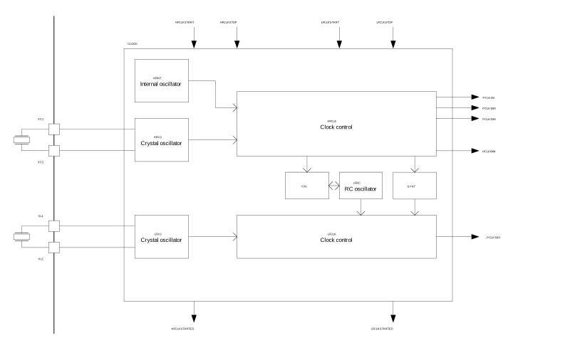
The HFCLK controller provides several clock signals in the system.
These are as follows:
- HCLK64M: 64 MHz CPU clock
- PCLK1M: 1 MHz peripheral clock
- PCLK16M: 16 MHz peripheral clock
- PCLK32M: 32 MHz peripheral clock
The HFCLK controller uses the following high frequency clock (HFCLK) sources:
- 64 MHz internal oscillator (HFINT)
- 64 MHz crystal oscillator (HFXO)
For illustration, see Clock control.
The HFCLK controller will automatically provide the clock(s) requested by the system. If the system does not request any clocks from the HFCLK controller, the controller will enter a power saving mode.
The HFINT source will be used when HFCLK is requested and HFXO has not been started.
- HFXO power-up time, as specified in 64 MHz crystal oscillator (HFXO).
- HFXO debounce time, as specified in register HFXODEBOUNCE.
The HFXO must be running to use the RADIO or the calibration mechanism associated with the 32.768 kHz RC oscillator.
64 MHz crystal oscillator (HFXO)
The 64 MHz crystal oscillator (HFXO) is controlled by a 32 MHz external crystal.
The crystal oscillator is designed for use with an AT-cut quartz crystal in parallel resonant mode. To achieve correct oscillation frequency, the load capacitance must match the specification in the crystal data sheet.
Circuit diagram of the 64 MHz crystal oscillator shows how the 32 MHz crystal is connected to the 64 MHz crystal oscillator.
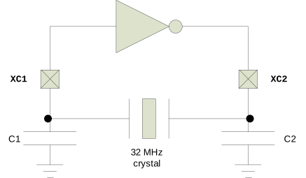
The load capacitance (CL) is the total capacitance seen by the crystal across its terminals and is given by:
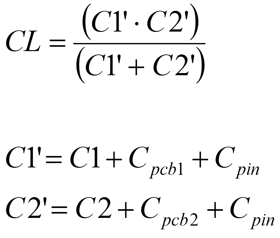
C1 and C2 are ceramic SMD capacitors connected between each crystal terminal and ground. For
more information, see Reference circuitry.
Cpcb1 and Cpcb2 are stray capacitances on the PCB. Cpin is the
pin input capacitance on the XC1 and XC2 pins. See table 64 MHz crystal oscillator (HFXO). The load capacitors C1
and C2 should have the same value.
For reliable operation, the crystal load capacitance, shunt capacitance, equivalent series resistance, and drive level must comply with the specifications in table 64 MHz crystal oscillator (HFXO). It is recommended to use a crystal with lower than maximum load capacitance and/or shunt capacitance. A low load capacitance will reduce both start up time and current consumption.
LFCLK controller
The system supports several low frequency clock sources.
As illustrated in Clock control, the system supports the following low frequency clock sources:
- 32.768 kHz RC oscillator (LFRC)
- 32.768 kHz crystal oscillator (LFXO)
- 32.768 kHz synthesized from HFCLK (LFSYNT)
The LFCLK controller and all of the LFCLK clock sources are always switched off when in System OFF mode.
The LFCLK clock is started by first selecting the preferred clock source in register LFCLKSRC and then triggering the LFCLKSTART task. If the LFXO is selected as the clock source, the LFCLK will initially start running from the 32.768 kHz LFRC while the LFXO is starting up and automatically switch to using the LFXO once this oscillator is running. The LFCLKSTARTED event will be generated when the LFXO has been started.
The register LFXODEBOUNCE is used to configure the LFXO debounce time. The register must be modified if operating in the Extended Operating Conditions temperature range, see Recommended operating conditions. The LFXO start up time will be increased as a result.
The LFCLK clock is stopped by triggering the LFCLKSTOP task.
Register LFCLKSRC controls the clock source, and its allowed swing. The truth table for various situations is as follows:
| SRC | EXTERNAL | BYPASS | Comment |
|---|---|---|---|
| 0 | 0 | 0 | Normal operation, LFRC is source |
| 0 | 0 | 1 | DO NOT USE |
| 0 | 1 | X | DO NOT USE |
| 1 | 0 | 0 | Normal XTAL operation |
| 1 | 1 | 0 | Apply external low swing signal to XL1, ground XL2 |
| 1 | 1 | 1 | Apply external full swing signal to XL1, leave XL2 grounded or unconnected |
| 1 | 0 | 1 | DO NOT USE |
| 2 | 0 | 0 | Normal operation, LFSYNT is source |
| 2 | 0 | 1 | DO NOT USE |
| 2 | 1 | X | DO NOT USE |
It is not allowed to write to register LFCLKSRC when the LFCLK is running.
A LFCLKSTOP task will stop the LFCLK oscillator. However, the LFCLKSTOP task can only be triggered after the STATE field in register LFCLKSTAT indicates LFCLK running state.
The synthesized 32.768 kHz clock depends on the HFCLK to run. If high accuracy is required for the LFCLK running off the synthesized 32.768 kHz clock, the HFCLK must running from the HFXO source.
32.768 kHz RC oscillator (LFRC)
The default source of the low frequency clock (LFCLK) is the 32.768 kHz RC oscillator (LFRC).
The LFRC oscillator does not require additional external components.
The LFRC frequency will be affected by variation in temperature. The LFRC oscillator can be calibrated to improve accuracy by using the HFXO as a reference oscillator during calibration.
Calibrating the 32.768 kHz RC oscillator
After the LFRC oscillator is started and running, it can be calibrated by triggering the CAL task.
The LFRC oscillator will then temporarily request the HFCLK to be used as a reference for the calibration. A DONE event will be generated when calibration has finished. The HFCLK crystal oscillator has to be started (by triggering the HFCLKSTART task) in order for the calibration mechanism to work.
It is not allowed to stop the LFRC during an ongoing calibration.
Calibration timer
The calibration timer can be used to time the calibration interval of the 32.768 kHz RC oscillator.
The calibration timer is started by triggering the CTSTART task and stopped by triggering the CTSTOP task. The calibration timer will always start counting down from the value specified in CTIV (Retained) and generate a CTTO event when it reaches 0. The calibration timer will automatically stop when it reaches 0.
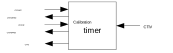
After a CTSTART task has been triggered, the calibration timer will ignore further tasks until it has returned the CTSTARTED event. Likewise, after a CTSTOP task has been triggered, the calibration timer will ignore further tasks until it has returned a CTSTOPPED event. Triggering CTSTART while the calibration timer is running will immediately return a CTSTARTED event. Triggering CTSTOP when the calibration timer is stopped will immediately return a CTSTOPPED event.
32.768 kHz crystal oscillator (LFXO)
For higher LFCLK accuracy (when better than +/- 500 ppm accuracy is required), the low frequency crystal oscillator (LFXO) must be used.
The following external clock sources are supported:
- Low swing clock signal applied to the XL1 pin. The XL2 pin shall then be grounded.
- Rail-to-rail clock signal applied to the XL1 pin. The XL2 pin shall then be grounded or left unconnected.
To achieve correct oscillation frequency, the load capacitance must match the specification in the crystal data sheet. Circuit diagram of the 32.768 kHz crystal oscillator shows the LFXO circuitry.
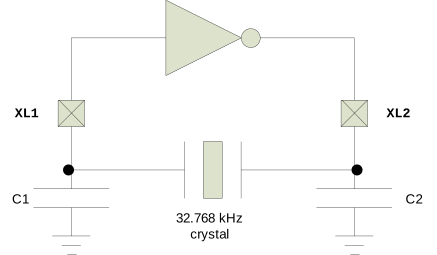
The load capacitance (CL) is the total capacitance seen by the crystal across its terminals and is given by:
C1 and C2 are ceramic SMD capacitors connected between each crystal terminal and ground. Cpcb1 and Cpcb2 are stray capacitances on the PCB. Cpin is the pin input capacitance on the XC1 and XC2 pins (see Low frequency crystal oscillator (LFXO)). The load capacitors C1 and C2 should have the same value.
For more information, see Reference circuitry.
32.768 kHz synthesized from HFCLK (LFSYNT)
LFCLK can also be synthesized from the HFCLK clock source. The accuracy of LFCLK will then be the accuracy of the HFCLK.
Using the LFSYNT clock avoids the requirement for a 32.768 kHz crystal, but increases average power consumption as the HFCLK will need to be requested in the system.
Registers
Instances
| Instance | Base address | Description |
|---|---|---|
| CLOCK | 0x40000000 | Clock control |
Register overview
| Register | Offset | Description |
|---|---|---|
| TASKS_HFCLKSTART | 0x000 | Start HFXO crystal oscillator |
| TASKS_HFCLKSTOP | 0x004 | Stop HFXO crystal oscillator |
| TASKS_LFCLKSTART | 0x008 | Start LFCLK |
| TASKS_LFCLKSTOP | 0x00C | Stop LFCLK |
| TASKS_CAL | 0x010 | Start calibration of LFRC |
| TASKS_CTSTART | 0x014 | Start calibration timer |
| TASKS_CTSTOP | 0x018 | Stop calibration timer |
| EVENTS_HFCLKSTARTED | 0x100 | HFXO crystal oscillator started |
| EVENTS_LFCLKSTARTED | 0x104 | LFCLK started |
| EVENTS_DONE | 0x10C | Calibration of LFRC completed |
| EVENTS_CTTO | 0x110 | Calibration timer timeout |
| EVENTS_CTSTARTED | 0x128 | Calibration timer has been started and is ready to process new tasks |
| EVENTS_CTSTOPPED | 0x12C | Calibration timer has been stopped and is ready to process new tasks |
| INTENSET | 0x304 | Enable interrupt |
| INTENCLR | 0x308 | Disable interrupt |
| HFCLKRUN | 0x408 | Status indicating that HFCLKSTART task has been triggered |
| HFCLKSTAT | 0x40C | HFCLK status |
| LFCLKRUN | 0x414 | Status indicating that LFCLKSTART task has been triggered |
| LFCLKSTAT | 0x418 | LFCLK status |
| LFCLKSRCCOPY | 0x41C | Copy of LFCLKSRC register, set when LFCLKSTART task was triggered |
| LFCLKSRC | 0x518 | Clock source for the LFCLK |
| HFXODEBOUNCE | 0x528 | HFXO debounce time. The HFXO is started by triggering the TASKS_HFCLKSTART task. |
| LFXODEBOUNCE | 0x52C | LFXO debounce time. The LFXO is started by triggering the TASKS_LFCLKSTART task when the LFCLKSRC register is configured for Xtal. |
| CTIV | 0x538 | Calibration timer interval This register is retained. |
| TRACECONFIG | 0x55C | Clocking options for the trace port debug interface |
TASKS_HFCLKSTART
Address offset: 0x000
Start HFXO crystal oscillator
| Bit number | 31 | 30 | 29 | 28 | 27 | 26 | 25 | 24 | 23 | 22 | 21 | 20 | 19 | 18 | 17 | 16 | 15 | 14 | 13 | 12 | 11 | 10 | 9 | 8 | 7 | 6 | 5 | 4 | 3 | 2 | 1 | 0 | |||
|---|---|---|---|---|---|---|---|---|---|---|---|---|---|---|---|---|---|---|---|---|---|---|---|---|---|---|---|---|---|---|---|---|---|---|---|
| ID | A | ||||||||||||||||||||||||||||||||||
| Reset 0x00000000 | 0 | 0 | 0 | 0 | 0 | 0 | 0 | 0 | 0 | 0 | 0 | 0 | 0 | 0 | 0 | 0 | 0 | 0 | 0 | 0 | 0 | 0 | 0 | 0 | 0 | 0 | 0 | 0 | 0 | 0 | 0 | 0 | |||
| ID | R/W | Field | Value ID | Value | Description | ||||||||||||||||||||||||||||||
| A | W | TASKS_HFCLKSTART | Start HFXO crystal oscillator | ||||||||||||||||||||||||||||||||
Trigger | 1 | Trigger task | |||||||||||||||||||||||||||||||||
TASKS_HFCLKSTOP
Address offset: 0x004
Stop HFXO crystal oscillator
| Bit number | 31 | 30 | 29 | 28 | 27 | 26 | 25 | 24 | 23 | 22 | 21 | 20 | 19 | 18 | 17 | 16 | 15 | 14 | 13 | 12 | 11 | 10 | 9 | 8 | 7 | 6 | 5 | 4 | 3 | 2 | 1 | 0 | |||
|---|---|---|---|---|---|---|---|---|---|---|---|---|---|---|---|---|---|---|---|---|---|---|---|---|---|---|---|---|---|---|---|---|---|---|---|
| ID | A | ||||||||||||||||||||||||||||||||||
| Reset 0x00000000 | 0 | 0 | 0 | 0 | 0 | 0 | 0 | 0 | 0 | 0 | 0 | 0 | 0 | 0 | 0 | 0 | 0 | 0 | 0 | 0 | 0 | 0 | 0 | 0 | 0 | 0 | 0 | 0 | 0 | 0 | 0 | 0 | |||
| ID | R/W | Field | Value ID | Value | Description | ||||||||||||||||||||||||||||||
| A | W | TASKS_HFCLKSTOP | Stop HFXO crystal oscillator | ||||||||||||||||||||||||||||||||
Trigger | 1 | Trigger task | |||||||||||||||||||||||||||||||||
TASKS_LFCLKSTART
Address offset: 0x008
Start LFCLK
| Bit number | 31 | 30 | 29 | 28 | 27 | 26 | 25 | 24 | 23 | 22 | 21 | 20 | 19 | 18 | 17 | 16 | 15 | 14 | 13 | 12 | 11 | 10 | 9 | 8 | 7 | 6 | 5 | 4 | 3 | 2 | 1 | 0 | |||
|---|---|---|---|---|---|---|---|---|---|---|---|---|---|---|---|---|---|---|---|---|---|---|---|---|---|---|---|---|---|---|---|---|---|---|---|
| ID | A | ||||||||||||||||||||||||||||||||||
| Reset 0x00000000 | 0 | 0 | 0 | 0 | 0 | 0 | 0 | 0 | 0 | 0 | 0 | 0 | 0 | 0 | 0 | 0 | 0 | 0 | 0 | 0 | 0 | 0 | 0 | 0 | 0 | 0 | 0 | 0 | 0 | 0 | 0 | 0 | |||
| ID | R/W | Field | Value ID | Value | Description | ||||||||||||||||||||||||||||||
| A | W | TASKS_LFCLKSTART | Start LFCLK | ||||||||||||||||||||||||||||||||
Trigger | 1 | Trigger task | |||||||||||||||||||||||||||||||||
TASKS_LFCLKSTOP
Address offset: 0x00C
Stop LFCLK
| Bit number | 31 | 30 | 29 | 28 | 27 | 26 | 25 | 24 | 23 | 22 | 21 | 20 | 19 | 18 | 17 | 16 | 15 | 14 | 13 | 12 | 11 | 10 | 9 | 8 | 7 | 6 | 5 | 4 | 3 | 2 | 1 | 0 | |||
|---|---|---|---|---|---|---|---|---|---|---|---|---|---|---|---|---|---|---|---|---|---|---|---|---|---|---|---|---|---|---|---|---|---|---|---|
| ID | A | ||||||||||||||||||||||||||||||||||
| Reset 0x00000000 | 0 | 0 | 0 | 0 | 0 | 0 | 0 | 0 | 0 | 0 | 0 | 0 | 0 | 0 | 0 | 0 | 0 | 0 | 0 | 0 | 0 | 0 | 0 | 0 | 0 | 0 | 0 | 0 | 0 | 0 | 0 | 0 | |||
| ID | R/W | Field | Value ID | Value | Description | ||||||||||||||||||||||||||||||
| A | W | TASKS_LFCLKSTOP | Stop LFCLK | ||||||||||||||||||||||||||||||||
Trigger | 1 | Trigger task | |||||||||||||||||||||||||||||||||
TASKS_CAL
Address offset: 0x010
Start calibration of LFRC
| Bit number | 31 | 30 | 29 | 28 | 27 | 26 | 25 | 24 | 23 | 22 | 21 | 20 | 19 | 18 | 17 | 16 | 15 | 14 | 13 | 12 | 11 | 10 | 9 | 8 | 7 | 6 | 5 | 4 | 3 | 2 | 1 | 0 | |||
|---|---|---|---|---|---|---|---|---|---|---|---|---|---|---|---|---|---|---|---|---|---|---|---|---|---|---|---|---|---|---|---|---|---|---|---|
| ID | A | ||||||||||||||||||||||||||||||||||
| Reset 0x00000000 | 0 | 0 | 0 | 0 | 0 | 0 | 0 | 0 | 0 | 0 | 0 | 0 | 0 | 0 | 0 | 0 | 0 | 0 | 0 | 0 | 0 | 0 | 0 | 0 | 0 | 0 | 0 | 0 | 0 | 0 | 0 | 0 | |||
| ID | R/W | Field | Value ID | Value | Description | ||||||||||||||||||||||||||||||
| A | W | TASKS_CAL | Start calibration of LFRC | ||||||||||||||||||||||||||||||||
Trigger | 1 | Trigger task | |||||||||||||||||||||||||||||||||
TASKS_CTSTART
Address offset: 0x014
Start calibration timer
| Bit number | 31 | 30 | 29 | 28 | 27 | 26 | 25 | 24 | 23 | 22 | 21 | 20 | 19 | 18 | 17 | 16 | 15 | 14 | 13 | 12 | 11 | 10 | 9 | 8 | 7 | 6 | 5 | 4 | 3 | 2 | 1 | 0 | |||
|---|---|---|---|---|---|---|---|---|---|---|---|---|---|---|---|---|---|---|---|---|---|---|---|---|---|---|---|---|---|---|---|---|---|---|---|
| ID | A | ||||||||||||||||||||||||||||||||||
| Reset 0x00000000 | 0 | 0 | 0 | 0 | 0 | 0 | 0 | 0 | 0 | 0 | 0 | 0 | 0 | 0 | 0 | 0 | 0 | 0 | 0 | 0 | 0 | 0 | 0 | 0 | 0 | 0 | 0 | 0 | 0 | 0 | 0 | 0 | |||
| ID | R/W | Field | Value ID | Value | Description | ||||||||||||||||||||||||||||||
| A | W | TASKS_CTSTART | Start calibration timer | ||||||||||||||||||||||||||||||||
Trigger | 1 | Trigger task | |||||||||||||||||||||||||||||||||
TASKS_CTSTOP
Address offset: 0x018
Stop calibration timer
| Bit number | 31 | 30 | 29 | 28 | 27 | 26 | 25 | 24 | 23 | 22 | 21 | 20 | 19 | 18 | 17 | 16 | 15 | 14 | 13 | 12 | 11 | 10 | 9 | 8 | 7 | 6 | 5 | 4 | 3 | 2 | 1 | 0 | |||
|---|---|---|---|---|---|---|---|---|---|---|---|---|---|---|---|---|---|---|---|---|---|---|---|---|---|---|---|---|---|---|---|---|---|---|---|
| ID | A | ||||||||||||||||||||||||||||||||||
| Reset 0x00000000 | 0 | 0 | 0 | 0 | 0 | 0 | 0 | 0 | 0 | 0 | 0 | 0 | 0 | 0 | 0 | 0 | 0 | 0 | 0 | 0 | 0 | 0 | 0 | 0 | 0 | 0 | 0 | 0 | 0 | 0 | 0 | 0 | |||
| ID | R/W | Field | Value ID | Value | Description | ||||||||||||||||||||||||||||||
| A | W | TASKS_CTSTOP | Stop calibration timer | ||||||||||||||||||||||||||||||||
Trigger | 1 | Trigger task | |||||||||||||||||||||||||||||||||
EVENTS_HFCLKSTARTED
Address offset: 0x100
HFXO crystal oscillator started
| Bit number | 31 | 30 | 29 | 28 | 27 | 26 | 25 | 24 | 23 | 22 | 21 | 20 | 19 | 18 | 17 | 16 | 15 | 14 | 13 | 12 | 11 | 10 | 9 | 8 | 7 | 6 | 5 | 4 | 3 | 2 | 1 | 0 | |||
|---|---|---|---|---|---|---|---|---|---|---|---|---|---|---|---|---|---|---|---|---|---|---|---|---|---|---|---|---|---|---|---|---|---|---|---|
| ID | A | ||||||||||||||||||||||||||||||||||
| Reset 0x00000000 | 0 | 0 | 0 | 0 | 0 | 0 | 0 | 0 | 0 | 0 | 0 | 0 | 0 | 0 | 0 | 0 | 0 | 0 | 0 | 0 | 0 | 0 | 0 | 0 | 0 | 0 | 0 | 0 | 0 | 0 | 0 | 0 | |||
| ID | R/W | Field | Value ID | Value | Description | ||||||||||||||||||||||||||||||
| A | RW | EVENTS_HFCLKSTARTED | HFXO crystal oscillator started | ||||||||||||||||||||||||||||||||
NotGenerated | 0 | Event not generated | |||||||||||||||||||||||||||||||||
Generated | 1 | Event generated | |||||||||||||||||||||||||||||||||
EVENTS_LFCLKSTARTED
Address offset: 0x104
LFCLK started
| Bit number | 31 | 30 | 29 | 28 | 27 | 26 | 25 | 24 | 23 | 22 | 21 | 20 | 19 | 18 | 17 | 16 | 15 | 14 | 13 | 12 | 11 | 10 | 9 | 8 | 7 | 6 | 5 | 4 | 3 | 2 | 1 | 0 | |||
|---|---|---|---|---|---|---|---|---|---|---|---|---|---|---|---|---|---|---|---|---|---|---|---|---|---|---|---|---|---|---|---|---|---|---|---|
| ID | A | ||||||||||||||||||||||||||||||||||
| Reset 0x00000000 | 0 | 0 | 0 | 0 | 0 | 0 | 0 | 0 | 0 | 0 | 0 | 0 | 0 | 0 | 0 | 0 | 0 | 0 | 0 | 0 | 0 | 0 | 0 | 0 | 0 | 0 | 0 | 0 | 0 | 0 | 0 | 0 | |||
| ID | R/W | Field | Value ID | Value | Description | ||||||||||||||||||||||||||||||
| A | RW | EVENTS_LFCLKSTARTED | LFCLK started | ||||||||||||||||||||||||||||||||
NotGenerated | 0 | Event not generated | |||||||||||||||||||||||||||||||||
Generated | 1 | Event generated | |||||||||||||||||||||||||||||||||
EVENTS_DONE
Address offset: 0x10C
Calibration of LFRC completed
| Bit number | 31 | 30 | 29 | 28 | 27 | 26 | 25 | 24 | 23 | 22 | 21 | 20 | 19 | 18 | 17 | 16 | 15 | 14 | 13 | 12 | 11 | 10 | 9 | 8 | 7 | 6 | 5 | 4 | 3 | 2 | 1 | 0 | |||
|---|---|---|---|---|---|---|---|---|---|---|---|---|---|---|---|---|---|---|---|---|---|---|---|---|---|---|---|---|---|---|---|---|---|---|---|
| ID | A | ||||||||||||||||||||||||||||||||||
| Reset 0x00000000 | 0 | 0 | 0 | 0 | 0 | 0 | 0 | 0 | 0 | 0 | 0 | 0 | 0 | 0 | 0 | 0 | 0 | 0 | 0 | 0 | 0 | 0 | 0 | 0 | 0 | 0 | 0 | 0 | 0 | 0 | 0 | 0 | |||
| ID | R/W | Field | Value ID | Value | Description | ||||||||||||||||||||||||||||||
| A | RW | EVENTS_DONE | Calibration of LFRC completed | ||||||||||||||||||||||||||||||||
NotGenerated | 0 | Event not generated | |||||||||||||||||||||||||||||||||
Generated | 1 | Event generated | |||||||||||||||||||||||||||||||||
EVENTS_CTTO
Address offset: 0x110
Calibration timer timeout
| Bit number | 31 | 30 | 29 | 28 | 27 | 26 | 25 | 24 | 23 | 22 | 21 | 20 | 19 | 18 | 17 | 16 | 15 | 14 | 13 | 12 | 11 | 10 | 9 | 8 | 7 | 6 | 5 | 4 | 3 | 2 | 1 | 0 | |||
|---|---|---|---|---|---|---|---|---|---|---|---|---|---|---|---|---|---|---|---|---|---|---|---|---|---|---|---|---|---|---|---|---|---|---|---|
| ID | A | ||||||||||||||||||||||||||||||||||
| Reset 0x00000000 | 0 | 0 | 0 | 0 | 0 | 0 | 0 | 0 | 0 | 0 | 0 | 0 | 0 | 0 | 0 | 0 | 0 | 0 | 0 | 0 | 0 | 0 | 0 | 0 | 0 | 0 | 0 | 0 | 0 | 0 | 0 | 0 | |||
| ID | R/W | Field | Value ID | Value | Description | ||||||||||||||||||||||||||||||
| A | RW | EVENTS_CTTO | Calibration timer timeout | ||||||||||||||||||||||||||||||||
NotGenerated | 0 | Event not generated | |||||||||||||||||||||||||||||||||
Generated | 1 | Event generated | |||||||||||||||||||||||||||||||||
EVENTS_CTSTARTED
Address offset: 0x128
Calibration timer has been started and is ready to process new tasks
| Bit number | 31 | 30 | 29 | 28 | 27 | 26 | 25 | 24 | 23 | 22 | 21 | 20 | 19 | 18 | 17 | 16 | 15 | 14 | 13 | 12 | 11 | 10 | 9 | 8 | 7 | 6 | 5 | 4 | 3 | 2 | 1 | 0 | |||
|---|---|---|---|---|---|---|---|---|---|---|---|---|---|---|---|---|---|---|---|---|---|---|---|---|---|---|---|---|---|---|---|---|---|---|---|
| ID | A | ||||||||||||||||||||||||||||||||||
| Reset 0x00000000 | 0 | 0 | 0 | 0 | 0 | 0 | 0 | 0 | 0 | 0 | 0 | 0 | 0 | 0 | 0 | 0 | 0 | 0 | 0 | 0 | 0 | 0 | 0 | 0 | 0 | 0 | 0 | 0 | 0 | 0 | 0 | 0 | |||
| ID | R/W | Field | Value ID | Value | Description | ||||||||||||||||||||||||||||||
| A | RW | EVENTS_CTSTARTED | Calibration timer has been started and is ready to process new tasks | ||||||||||||||||||||||||||||||||
NotGenerated | 0 | Event not generated | |||||||||||||||||||||||||||||||||
Generated | 1 | Event generated | |||||||||||||||||||||||||||||||||
EVENTS_CTSTOPPED
Address offset: 0x12C
Calibration timer has been stopped and is ready to process new tasks
| Bit number | 31 | 30 | 29 | 28 | 27 | 26 | 25 | 24 | 23 | 22 | 21 | 20 | 19 | 18 | 17 | 16 | 15 | 14 | 13 | 12 | 11 | 10 | 9 | 8 | 7 | 6 | 5 | 4 | 3 | 2 | 1 | 0 | |||
|---|---|---|---|---|---|---|---|---|---|---|---|---|---|---|---|---|---|---|---|---|---|---|---|---|---|---|---|---|---|---|---|---|---|---|---|
| ID | A | ||||||||||||||||||||||||||||||||||
| Reset 0x00000000 | 0 | 0 | 0 | 0 | 0 | 0 | 0 | 0 | 0 | 0 | 0 | 0 | 0 | 0 | 0 | 0 | 0 | 0 | 0 | 0 | 0 | 0 | 0 | 0 | 0 | 0 | 0 | 0 | 0 | 0 | 0 | 0 | |||
| ID | R/W | Field | Value ID | Value | Description | ||||||||||||||||||||||||||||||
| A | RW | EVENTS_CTSTOPPED | Calibration timer has been stopped and is ready to process new tasks | ||||||||||||||||||||||||||||||||
NotGenerated | 0 | Event not generated | |||||||||||||||||||||||||||||||||
Generated | 1 | Event generated | |||||||||||||||||||||||||||||||||
INTENSET
Address offset: 0x304
Enable interrupt
| Bit number | 31 | 30 | 29 | 28 | 27 | 26 | 25 | 24 | 23 | 22 | 21 | 20 | 19 | 18 | 17 | 16 | 15 | 14 | 13 | 12 | 11 | 10 | 9 | 8 | 7 | 6 | 5 | 4 | 3 | 2 | 1 | 0 | |||
|---|---|---|---|---|---|---|---|---|---|---|---|---|---|---|---|---|---|---|---|---|---|---|---|---|---|---|---|---|---|---|---|---|---|---|---|
| ID | F | E | D | C | B | A | |||||||||||||||||||||||||||||
| Reset 0x00000000 | 0 | 0 | 0 | 0 | 0 | 0 | 0 | 0 | 0 | 0 | 0 | 0 | 0 | 0 | 0 | 0 | 0 | 0 | 0 | 0 | 0 | 0 | 0 | 0 | 0 | 0 | 0 | 0 | 0 | 0 | 0 | 0 | |||
| ID | R/W | Field | Value ID | Value | Description | ||||||||||||||||||||||||||||||
| A | RW | HFCLKSTARTED | Write '1' to enable interrupt for event HFCLKSTARTED | ||||||||||||||||||||||||||||||||
Set | 1 | Enable | |||||||||||||||||||||||||||||||||
Disabled | 0 | Read: Disabled | |||||||||||||||||||||||||||||||||
Enabled | 1 | Read: Enabled | |||||||||||||||||||||||||||||||||
| B | RW | LFCLKSTARTED | Write '1' to enable interrupt for event LFCLKSTARTED | ||||||||||||||||||||||||||||||||
Set | 1 | Enable | |||||||||||||||||||||||||||||||||
Disabled | 0 | Read: Disabled | |||||||||||||||||||||||||||||||||
Enabled | 1 | Read: Enabled | |||||||||||||||||||||||||||||||||
| C | RW | DONE | Write '1' to enable interrupt for event DONE | ||||||||||||||||||||||||||||||||
Set | 1 | Enable | |||||||||||||||||||||||||||||||||
Disabled | 0 | Read: Disabled | |||||||||||||||||||||||||||||||||
Enabled | 1 | Read: Enabled | |||||||||||||||||||||||||||||||||
| D | RW | CTTO | Write '1' to enable interrupt for event CTTO | ||||||||||||||||||||||||||||||||
Set | 1 | Enable | |||||||||||||||||||||||||||||||||
Disabled | 0 | Read: Disabled | |||||||||||||||||||||||||||||||||
Enabled | 1 | Read: Enabled | |||||||||||||||||||||||||||||||||
| E | RW | CTSTARTED | Write '1' to enable interrupt for event CTSTARTED | ||||||||||||||||||||||||||||||||
Set | 1 | Enable | |||||||||||||||||||||||||||||||||
Disabled | 0 | Read: Disabled | |||||||||||||||||||||||||||||||||
Enabled | 1 | Read: Enabled | |||||||||||||||||||||||||||||||||
| F | RW | CTSTOPPED | Write '1' to enable interrupt for event CTSTOPPED | ||||||||||||||||||||||||||||||||
Set | 1 | Enable | |||||||||||||||||||||||||||||||||
Disabled | 0 | Read: Disabled | |||||||||||||||||||||||||||||||||
Enabled | 1 | Read: Enabled | |||||||||||||||||||||||||||||||||
INTENCLR
Address offset: 0x308
Disable interrupt
| Bit number | 31 | 30 | 29 | 28 | 27 | 26 | 25 | 24 | 23 | 22 | 21 | 20 | 19 | 18 | 17 | 16 | 15 | 14 | 13 | 12 | 11 | 10 | 9 | 8 | 7 | 6 | 5 | 4 | 3 | 2 | 1 | 0 | |||
|---|---|---|---|---|---|---|---|---|---|---|---|---|---|---|---|---|---|---|---|---|---|---|---|---|---|---|---|---|---|---|---|---|---|---|---|
| ID | F | E | D | C | B | A | |||||||||||||||||||||||||||||
| Reset 0x00000000 | 0 | 0 | 0 | 0 | 0 | 0 | 0 | 0 | 0 | 0 | 0 | 0 | 0 | 0 | 0 | 0 | 0 | 0 | 0 | 0 | 0 | 0 | 0 | 0 | 0 | 0 | 0 | 0 | 0 | 0 | 0 | 0 | |||
| ID | R/W | Field | Value ID | Value | Description | ||||||||||||||||||||||||||||||
| A | RW | HFCLKSTARTED | Write '1' to disable interrupt for event HFCLKSTARTED | ||||||||||||||||||||||||||||||||
Clear | 1 | Disable | |||||||||||||||||||||||||||||||||
Disabled | 0 | Read: Disabled | |||||||||||||||||||||||||||||||||
Enabled | 1 | Read: Enabled | |||||||||||||||||||||||||||||||||
| B | RW | LFCLKSTARTED | Write '1' to disable interrupt for event LFCLKSTARTED | ||||||||||||||||||||||||||||||||
Clear | 1 | Disable | |||||||||||||||||||||||||||||||||
Disabled | 0 | Read: Disabled | |||||||||||||||||||||||||||||||||
Enabled | 1 | Read: Enabled | |||||||||||||||||||||||||||||||||
| C | RW | DONE | Write '1' to disable interrupt for event DONE | ||||||||||||||||||||||||||||||||
Clear | 1 | Disable | |||||||||||||||||||||||||||||||||
Disabled | 0 | Read: Disabled | |||||||||||||||||||||||||||||||||
Enabled | 1 | Read: Enabled | |||||||||||||||||||||||||||||||||
| D | RW | CTTO | Write '1' to disable interrupt for event CTTO | ||||||||||||||||||||||||||||||||
Clear | 1 | Disable | |||||||||||||||||||||||||||||||||
Disabled | 0 | Read: Disabled | |||||||||||||||||||||||||||||||||
Enabled | 1 | Read: Enabled | |||||||||||||||||||||||||||||||||
| E | RW | CTSTARTED | Write '1' to disable interrupt for event CTSTARTED | ||||||||||||||||||||||||||||||||
Clear | 1 | Disable | |||||||||||||||||||||||||||||||||
Disabled | 0 | Read: Disabled | |||||||||||||||||||||||||||||||||
Enabled | 1 | Read: Enabled | |||||||||||||||||||||||||||||||||
| F | RW | CTSTOPPED | Write '1' to disable interrupt for event CTSTOPPED | ||||||||||||||||||||||||||||||||
Clear | 1 | Disable | |||||||||||||||||||||||||||||||||
Disabled | 0 | Read: Disabled | |||||||||||||||||||||||||||||||||
Enabled | 1 | Read: Enabled | |||||||||||||||||||||||||||||||||
HFCLKRUN
Address offset: 0x408
Status indicating that HFCLKSTART task has been triggered
| Bit number | 31 | 30 | 29 | 28 | 27 | 26 | 25 | 24 | 23 | 22 | 21 | 20 | 19 | 18 | 17 | 16 | 15 | 14 | 13 | 12 | 11 | 10 | 9 | 8 | 7 | 6 | 5 | 4 | 3 | 2 | 1 | 0 | |||
|---|---|---|---|---|---|---|---|---|---|---|---|---|---|---|---|---|---|---|---|---|---|---|---|---|---|---|---|---|---|---|---|---|---|---|---|
| ID | A | ||||||||||||||||||||||||||||||||||
| Reset 0x00000000 | 0 | 0 | 0 | 0 | 0 | 0 | 0 | 0 | 0 | 0 | 0 | 0 | 0 | 0 | 0 | 0 | 0 | 0 | 0 | 0 | 0 | 0 | 0 | 0 | 0 | 0 | 0 | 0 | 0 | 0 | 0 | 0 | |||
| ID | R/W | Field | Value ID | Value | Description | ||||||||||||||||||||||||||||||
| A | R | STATUS | HFCLKSTART task triggered or not | ||||||||||||||||||||||||||||||||
NotTriggered | 0 | Task not triggered | |||||||||||||||||||||||||||||||||
Triggered | 1 | Task triggered | |||||||||||||||||||||||||||||||||
HFCLKSTAT
Address offset: 0x40C
HFCLK status
| Bit number | 31 | 30 | 29 | 28 | 27 | 26 | 25 | 24 | 23 | 22 | 21 | 20 | 19 | 18 | 17 | 16 | 15 | 14 | 13 | 12 | 11 | 10 | 9 | 8 | 7 | 6 | 5 | 4 | 3 | 2 | 1 | 0 | |||
|---|---|---|---|---|---|---|---|---|---|---|---|---|---|---|---|---|---|---|---|---|---|---|---|---|---|---|---|---|---|---|---|---|---|---|---|
| ID | B | A | |||||||||||||||||||||||||||||||||
| Reset 0x00000000 | 0 | 0 | 0 | 0 | 0 | 0 | 0 | 0 | 0 | 0 | 0 | 0 | 0 | 0 | 0 | 0 | 0 | 0 | 0 | 0 | 0 | 0 | 0 | 0 | 0 | 0 | 0 | 0 | 0 | 0 | 0 | 0 | |||
| ID | R/W | Field | Value ID | Value | Description | ||||||||||||||||||||||||||||||
| A | R | SRC | Source of HFCLK | ||||||||||||||||||||||||||||||||
RC | 0 | 64 MHz internal oscillator (HFINT) | |||||||||||||||||||||||||||||||||
Xtal | 1 | 64 MHz crystal oscillator (HFXO) | |||||||||||||||||||||||||||||||||
| B | R | STATE | HFCLK state | ||||||||||||||||||||||||||||||||
NotRunning | 0 | HFCLK not running | |||||||||||||||||||||||||||||||||
Running | 1 | HFCLK running | |||||||||||||||||||||||||||||||||
LFCLKRUN
Address offset: 0x414
Status indicating that LFCLKSTART task has been triggered
| Bit number | 31 | 30 | 29 | 28 | 27 | 26 | 25 | 24 | 23 | 22 | 21 | 20 | 19 | 18 | 17 | 16 | 15 | 14 | 13 | 12 | 11 | 10 | 9 | 8 | 7 | 6 | 5 | 4 | 3 | 2 | 1 | 0 | |||
|---|---|---|---|---|---|---|---|---|---|---|---|---|---|---|---|---|---|---|---|---|---|---|---|---|---|---|---|---|---|---|---|---|---|---|---|
| ID | A | ||||||||||||||||||||||||||||||||||
| Reset 0x00000000 | 0 | 0 | 0 | 0 | 0 | 0 | 0 | 0 | 0 | 0 | 0 | 0 | 0 | 0 | 0 | 0 | 0 | 0 | 0 | 0 | 0 | 0 | 0 | 0 | 0 | 0 | 0 | 0 | 0 | 0 | 0 | 0 | |||
| ID | R/W | Field | Value ID | Value | Description | ||||||||||||||||||||||||||||||
| A | R | STATUS | LFCLKSTART task triggered or not | ||||||||||||||||||||||||||||||||
NotTriggered | 0 | Task not triggered | |||||||||||||||||||||||||||||||||
Triggered | 1 | Task triggered | |||||||||||||||||||||||||||||||||
LFCLKSTAT
Address offset: 0x418
LFCLK status
| Bit number | 31 | 30 | 29 | 28 | 27 | 26 | 25 | 24 | 23 | 22 | 21 | 20 | 19 | 18 | 17 | 16 | 15 | 14 | 13 | 12 | 11 | 10 | 9 | 8 | 7 | 6 | 5 | 4 | 3 | 2 | 1 | 0 | |||
|---|---|---|---|---|---|---|---|---|---|---|---|---|---|---|---|---|---|---|---|---|---|---|---|---|---|---|---|---|---|---|---|---|---|---|---|
| ID | B | A | A | ||||||||||||||||||||||||||||||||
| Reset 0x00000000 | 0 | 0 | 0 | 0 | 0 | 0 | 0 | 0 | 0 | 0 | 0 | 0 | 0 | 0 | 0 | 0 | 0 | 0 | 0 | 0 | 0 | 0 | 0 | 0 | 0 | 0 | 0 | 0 | 0 | 0 | 0 | 0 | |||
| ID | R/W | Field | Value ID | Value | Description | ||||||||||||||||||||||||||||||
| A | R | SRC | Source of LFCLK | ||||||||||||||||||||||||||||||||
RC | 0 | 32.768 kHz RC oscillator (LFRC) | |||||||||||||||||||||||||||||||||
Xtal | 1 | 32.768 kHz crystal oscillator (LFXO) | |||||||||||||||||||||||||||||||||
Synth | 2 | 32.768 kHz synthesized from HFCLK (LFSYNT) | |||||||||||||||||||||||||||||||||
| B | R | STATE | LFCLK state | ||||||||||||||||||||||||||||||||
NotRunning | 0 | LFCLK not running | |||||||||||||||||||||||||||||||||
Running | 1 | LFCLK running | |||||||||||||||||||||||||||||||||
LFCLKSRCCOPY
Address offset: 0x41C
Copy of LFCLKSRC register, set when LFCLKSTART task was triggered
| Bit number | 31 | 30 | 29 | 28 | 27 | 26 | 25 | 24 | 23 | 22 | 21 | 20 | 19 | 18 | 17 | 16 | 15 | 14 | 13 | 12 | 11 | 10 | 9 | 8 | 7 | 6 | 5 | 4 | 3 | 2 | 1 | 0 | |||
|---|---|---|---|---|---|---|---|---|---|---|---|---|---|---|---|---|---|---|---|---|---|---|---|---|---|---|---|---|---|---|---|---|---|---|---|
| ID | A | A | |||||||||||||||||||||||||||||||||
| Reset 0x00000000 | 0 | 0 | 0 | 0 | 0 | 0 | 0 | 0 | 0 | 0 | 0 | 0 | 0 | 0 | 0 | 0 | 0 | 0 | 0 | 0 | 0 | 0 | 0 | 0 | 0 | 0 | 0 | 0 | 0 | 0 | 0 | 0 | |||
| ID | R/W | Field | Value ID | Value | Description | ||||||||||||||||||||||||||||||
| A | R | SRC | Clock source | ||||||||||||||||||||||||||||||||
RC | 0 | 32.768 kHz RC oscillator (LFRC) | |||||||||||||||||||||||||||||||||
Xtal | 1 | 32.768 kHz crystal oscillator (LFXO) | |||||||||||||||||||||||||||||||||
Synth | 2 | 32.768 kHz synthesized from HFCLK (LFSYNT) | |||||||||||||||||||||||||||||||||
LFCLKSRC
Address offset: 0x518
Clock source for the LFCLK
| Bit number | 31 | 30 | 29 | 28 | 27 | 26 | 25 | 24 | 23 | 22 | 21 | 20 | 19 | 18 | 17 | 16 | 15 | 14 | 13 | 12 | 11 | 10 | 9 | 8 | 7 | 6 | 5 | 4 | 3 | 2 | 1 | 0 | |||
|---|---|---|---|---|---|---|---|---|---|---|---|---|---|---|---|---|---|---|---|---|---|---|---|---|---|---|---|---|---|---|---|---|---|---|---|
| ID | C | B | A | A | |||||||||||||||||||||||||||||||
| Reset 0x00000000 | 0 | 0 | 0 | 0 | 0 | 0 | 0 | 0 | 0 | 0 | 0 | 0 | 0 | 0 | 0 | 0 | 0 | 0 | 0 | 0 | 0 | 0 | 0 | 0 | 0 | 0 | 0 | 0 | 0 | 0 | 0 | 0 | |||
| ID | R/W | Field | Value ID | Value | Description | ||||||||||||||||||||||||||||||
| A | RW | SRC | Clock source | ||||||||||||||||||||||||||||||||
RC | 0 | 32.768 kHz RC oscillator (LFRC) | |||||||||||||||||||||||||||||||||
Xtal | 1 | 32.768 kHz crystal oscillator (LFXO) | |||||||||||||||||||||||||||||||||
Synth | 2 | 32.768 kHz synthesized from HFCLK (LFSYNT) | |||||||||||||||||||||||||||||||||
| B | RW | BYPASS | Enable or disable bypass of LFCLK crystal oscillator with external clock source | ||||||||||||||||||||||||||||||||
Disabled | 0 | Disable (use with Xtal or low-swing external source) | |||||||||||||||||||||||||||||||||
Enabled | 1 | Enable (use with rail-to-rail external source) | |||||||||||||||||||||||||||||||||
| C | RW | EXTERNAL | Enable or disable external source for LFCLK | ||||||||||||||||||||||||||||||||
Disabled | 0 | Disable external source (use with Xtal) | |||||||||||||||||||||||||||||||||
Enabled | 1 | Enable use of external source instead of Xtal (SRC needs to be set to Xtal) | |||||||||||||||||||||||||||||||||
HFXODEBOUNCE
Address offset: 0x528
HFXO debounce time. The HFXO is started by triggering the TASKS_HFCLKSTART task.
The EVENTS_HFCLKSTARTED event is generated after the HFXO power up time + the HFXO debounce time has elapsed. It is not allowed to change the value of this register while the HFXO is starting.
| Bit number | 31 | 30 | 29 | 28 | 27 | 26 | 25 | 24 | 23 | 22 | 21 | 20 | 19 | 18 | 17 | 16 | 15 | 14 | 13 | 12 | 11 | 10 | 9 | 8 | 7 | 6 | 5 | 4 | 3 | 2 | 1 | 0 | |||
|---|---|---|---|---|---|---|---|---|---|---|---|---|---|---|---|---|---|---|---|---|---|---|---|---|---|---|---|---|---|---|---|---|---|---|---|
| ID | A | A | A | A | A | A | A | A | |||||||||||||||||||||||||||
| Reset 0x00000010 | 0 | 0 | 0 | 0 | 0 | 0 | 0 | 0 | 0 | 0 | 0 | 0 | 0 | 0 | 0 | 0 | 0 | 0 | 0 | 0 | 0 | 0 | 0 | 0 | 0 | 0 | 0 | 1 | 0 | 0 | 0 | 0 | |||
| ID | R/W | Field | Value ID | Value | Description | ||||||||||||||||||||||||||||||
| A | RW | HFXODEBOUNCE | 0x01..0xFF | HFXO debounce time. Debounce time = HFXODEBOUNCE * 16 µs. | |||||||||||||||||||||||||||||||
Db256us | 0x10 | 256 µs debounce time. Recommended for 1.6 mm x 2.0 mm crystals and larger. | |||||||||||||||||||||||||||||||||
Db1024us | 0x40 | 1024 µs debounce time. Recommended for 1.6 mm x 1.2 mm crystals and smaller. | |||||||||||||||||||||||||||||||||
LFXODEBOUNCE
Address offset: 0x52C
LFXO debounce time. The LFXO is started by triggering the TASKS_LFCLKSTART task when the LFCLKSRC register is configured for Xtal.
The EVENTS_LFCLKSTARTED event is generated after the LFXO debounce time has elapsed. It is not allowed to change the value of this register while the LFXO is starting.
| Bit number | 31 | 30 | 29 | 28 | 27 | 26 | 25 | 24 | 23 | 22 | 21 | 20 | 19 | 18 | 17 | 16 | 15 | 14 | 13 | 12 | 11 | 10 | 9 | 8 | 7 | 6 | 5 | 4 | 3 | 2 | 1 | 0 | |||
|---|---|---|---|---|---|---|---|---|---|---|---|---|---|---|---|---|---|---|---|---|---|---|---|---|---|---|---|---|---|---|---|---|---|---|---|
| ID | A | ||||||||||||||||||||||||||||||||||
| Reset 0x00000000 | 0 | 0 | 0 | 0 | 0 | 0 | 0 | 0 | 0 | 0 | 0 | 0 | 0 | 0 | 0 | 0 | 0 | 0 | 0 | 0 | 0 | 0 | 0 | 0 | 0 | 0 | 0 | 0 | 0 | 0 | 0 | 0 | |||
| ID | R/W | Field | Value ID | Value | Description | ||||||||||||||||||||||||||||||
| A | RW | LFXODEBOUNCE | LFXO debounce time. | ||||||||||||||||||||||||||||||||
Normal | 0 | 8192 32.768 kHz periods, or 0.25 s. Recommended for normal Operating Temperature conditions. | |||||||||||||||||||||||||||||||||
Extended | 1 | 16384 32.768 kHz periods, or 0.5 s. Recommended for Extended Operating Temperature conditions. | |||||||||||||||||||||||||||||||||
CTIV (Retained)
Address offset: 0x538
Calibration timer interval
This register is retained.
| Bit number | 31 | 30 | 29 | 28 | 27 | 26 | 25 | 24 | 23 | 22 | 21 | 20 | 19 | 18 | 17 | 16 | 15 | 14 | 13 | 12 | 11 | 10 | 9 | 8 | 7 | 6 | 5 | 4 | 3 | 2 | 1 | 0 | |||
|---|---|---|---|---|---|---|---|---|---|---|---|---|---|---|---|---|---|---|---|---|---|---|---|---|---|---|---|---|---|---|---|---|---|---|---|
| ID | A | A | A | A | A | A | A | ||||||||||||||||||||||||||||
| Reset 0x00000000 | 0 | 0 | 0 | 0 | 0 | 0 | 0 | 0 | 0 | 0 | 0 | 0 | 0 | 0 | 0 | 0 | 0 | 0 | 0 | 0 | 0 | 0 | 0 | 0 | 0 | 0 | 0 | 0 | 0 | 0 | 0 | 0 | |||
| ID | R/W | Field | Value ID | Value | Description | ||||||||||||||||||||||||||||||
| A | RW | CTIV | Calibration timer interval in multiple of 0.25 seconds. Range: 0.25 seconds to 31.75 seconds. | ||||||||||||||||||||||||||||||||
TRACECONFIG
Address offset: 0x55C
Clocking options for the trace port debug interface
This register is a retained register. Reset behavior is the same as debug components.
| Bit number | 31 | 30 | 29 | 28 | 27 | 26 | 25 | 24 | 23 | 22 | 21 | 20 | 19 | 18 | 17 | 16 | 15 | 14 | 13 | 12 | 11 | 10 | 9 | 8 | 7 | 6 | 5 | 4 | 3 | 2 | 1 | 0 | |||
|---|---|---|---|---|---|---|---|---|---|---|---|---|---|---|---|---|---|---|---|---|---|---|---|---|---|---|---|---|---|---|---|---|---|---|---|
| ID | B | B | A | A | |||||||||||||||||||||||||||||||
| Reset 0x00000000 | 0 | 0 | 0 | 0 | 0 | 0 | 0 | 0 | 0 | 0 | 0 | 0 | 0 | 0 | 0 | 0 | 0 | 0 | 0 | 0 | 0 | 0 | 0 | 0 | 0 | 0 | 0 | 0 | 0 | 0 | 0 | 0 | |||
| ID | R/W | Field | Value ID | Value | Description | ||||||||||||||||||||||||||||||
| A | RW | TRACEPORTSPEED | Speed of trace port clock. Note that the TRACECLK pin will output this clock divided by two. | ||||||||||||||||||||||||||||||||
32MHz | 0 | 32 MHz trace port clock (TRACECLK = 16 MHz) | |||||||||||||||||||||||||||||||||
16MHz | 1 | 16 MHz trace port clock (TRACECLK = 8 MHz) | |||||||||||||||||||||||||||||||||
8MHz | 2 | 8 MHz trace port clock (TRACECLK = 4 MHz) | |||||||||||||||||||||||||||||||||
4MHz | 3 | 4 MHz trace port clock (TRACECLK = 2 MHz) | |||||||||||||||||||||||||||||||||
| B | RW | TRACEMUX | Pin multiplexing of trace signals. See pin assignment chapter for more details. | ||||||||||||||||||||||||||||||||
GPIO | 0 | No trace signals routed to pins. All pins can be used as regular GPIOs. | |||||||||||||||||||||||||||||||||
Serial | 1 | SWO trace signal routed to pin. Remaining pins can be used as regular GPIOs. | |||||||||||||||||||||||||||||||||
Parallel | 2 | All trace signals (TRACECLK and TRACEDATA[n]) routed to pins. | |||||||||||||||||||||||||||||||||
Electrical specification
64 MHz internal oscillator (HFINT)
| Symbol | Description | Min. | Typ. | Max. | Units |
|---|---|---|---|---|---|
| fNOM_HFINT | Nominal output frequency | 64 | MHz | ||
| fTOL_HFINT | Frequency tolerance | ±1.5 | ±8 | % | |
| fTOL_HFINT,EXT | Frequency tolerance, extended temperature range | ±9 | % |
64 MHz crystal oscillator (HFXO)
| Symbol | Description | Min. | Typ. | Max. | Units |
|---|---|---|---|---|---|
| fNOM_HFXO | Nominal output frequency | 64 | MHz | ||
| fXTAL_HFXO | External crystal frequency | 32 | MHz | ||
| fTOL_HFXO | Frequency tolerance requirement for 2.4 GHz proprietary radio applications | ±60 | ppm | ||
| fTOL_HFXO_BLE | Frequency tolerance requirement, Bluetooth low energy applications, packet length ≤ 200 bytes | ±40 | ppm | ||
| fTOL_HFXO_BLE_LP | Frequency tolerance requirement, Bluetooth low energy applications, packet length > 200 bytes | ±30 | ppm | ||
| CL_HFXO | Load capacitance | 12 | pF | ||
| C0_HFXO | Shunt capacitance | 7 | pF | ||
| RS_HFXO_7PF | Equivalent series resistance 3 pF < C0 ≤ 7 pF | 60 | Ω | ||
| RS_HFXO_3PF | Equivalent series resistance C0 ≤ 3 pF | 100 | Ω | ||
| PD_HFXO | Drive level | 100 | µW | ||
| CPIN_HFXO | Input capacitance XC1 and XC2 | 3 | pF | ||
| ISTBY_X32M | Core standby current for various crystals | ||||
| ISTBY_X32M_X0 | Typical parameters for a given 2.5mm x 2.0mm crystal: CL_HFXO = 8 pF, C0_HFXO = 1 pF, LM_HFXO = 7 mH, RS_HFXO = 20 Ω | 65 | µA | ||
| ISTBY_X32M_X1 | Typical parameters for a given 1.6mm x 1.2mm crystal: CL_HFXO = 8 pF, C0_HFXO = 0.4 pF, LM_HFXO = 20 mH, RS_HFXO = 40 Ω | 110 | µA | ||
| ISTART_X32M | Average startup current for various crystals, first 1 ms | ||||
| ISTART_X32M_X0 | Typical parameters for a given 2.5mm x 2.0mm crystal: CL_HFXO = 8 pF, C0_HFXO = 1 pF, LM_HFXO = 7 mH, RS_HFXO = 20 Ω | 360 | µA | ||
| ISTART_X32M_X1 | Typical parameters for a given 1.6mm x 1.2mm crystal: CL_HFXO = 8 pF, C0_HFXO = 0.4 pF, LM_HFXO = 20 mH, RS_HFXO = 40 Ω | 785 | µA | ||
| tPOWERUP_X32M | Power-up time for various crystals | ||||
| tPOWERUP_X32M_X0 | Typical parameters for a given 2.5mm x 2.0mm crystal: CL_HFXO = 8 pF, C0_HFXO = 1 pF, LM_HFXO = 7 mH, RS_HFXO = 20 Ω | 60 | µs | ||
| tPOWERUP_X32M_X1 | Typical parameters for a given 1.6mm x 1.2mm crystal: CL_HFXO = 8 pF, C0_HFXO = 0.4 pF, LM_HFXO = 20 mH, RS_HFXO = 40 Ω | 200 | µs |
Low frequency crystal oscillator (LFXO)
| Symbol | Description | Min. | Typ. | Max. | Units |
|---|---|---|---|---|---|
| fNOM_LFXO | Crystal frequency | 32.768 | kHz | ||
| fTOL_LFXO_BLE | Frequency tolerance requirement for BLE stack | ±500 | ppm | ||
| fTOL_LFXO_ANT | Frequency tolerance requirement for ANT stack | ±50 | ppm | ||
| CL_LFXO | Load capacitance | 12.5 | pF | ||
| C0_LFXO | Shunt capacitance | 2 | pF | ||
| RS_LFXO | Equivalent series resistance | 100 | kΩ | ||
| PD_LFXO | Drive level | 0.5 | μW | ||
| Cpin | Input capacitance on XL1 and XL2 pads | 4 | pF | ||
| ILFXO | Run current for 32.768 kHz crystal oscillator | 0.23 | µA | ||
| tSTART_LFXO | Startup time for 32.768 kHz crystal oscillator | 0.25 | s | ||
| tSTART_LFXO_EXT | Startup time for 32.768 kHz crystal oscillator when CLOCK.LFXODEBOUNCE configured for Extended debounce time | 0.5 | s | ||
| VAMP,IN,XO,LOW | Peak to peak amplitude for external low swing clock. Input signal must not swing outside supply rails. | 200 | 1000 | mV |
Low frequency RC oscillator (LFRC)
| Symbol | Description | Min. | Typ. | Max. | Units |
|---|---|---|---|---|---|
| fNOM_LFRC | Nominal frequency | 32.768 | kHz | ||
| fTOL_LFRC | Frequency tolerance, uncalibrated | ±5 | % | ||
| fTOL_CAL_LFRC | Frequency tolerance after calibration1 | ±500 | ppm | ||
| ILFRC | Run current | 0.7 | µA | ||
| tSTART_LFRC | Startup time | 1000 | μs |
Synthesized low frequency clock (LFSYNT)
| Symbol | Description | Min. | Typ. | Max. | Units |
|---|---|---|---|---|---|
| fNOM_LFSYNT | Nominal frequency | 32.768 | kHz |