PDM — Pulse density modulation interface
The pulse density modulation (PDM) module enables input of pulse density modulated signals from external audio frontends, for example, digital microphones. The PDM module generates the PDM clock and supports single-channel or dual-channel (left and right) data input. Data is transferred directly to RAM buffers using EasyDMA.
Listed here are the main features for PDM:
- Up to two PDM microphones configured as a left/right pair using the same data input
- 16 kHz output sample rate, 16-bit samples
- EasyDMA support for sample buffering
- HW decimation filters
- Selectable ratio of 64 or 80 between PDM_CLK and output sample rate
The PDM module illustrated below is interfacing up to two digital microphones with the PDM interface. EasyDMA is implemented to relieve the real-time requirements associated with controlling of the PDM slave from a low priority CPU execution context. It also includes all the necessary digital filter elements to produce pulse code modulation (PCM) samples. The PDM module allows continuous audio streaming.
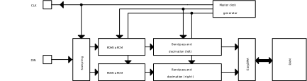
Master clock generator
The master clock generator's PDMCLKCTRL register allows adjusting the PDM clock's frequency.
The master clock generator does not add any jitter to the HFCLK source chosen. It is recommended (but not mandatory) to use the Xtal as HFCLK source.
Module operation
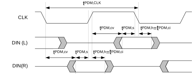
By default, bits from the left PDM microphone are sampled on PDM_CLK falling edge, and bits for the right are sampled on the rising edge of PDM_CLK, resulting in two bitstreams. Each bitstream is fed into a digital filter which converts the PDM stream into 16-bit PCM samples, then filters and down-samples them to reach the appropriate sample rate.
The EDGE field in the MODE register allows swapping left and right, so that left will be sampled on rising edge, and right on falling.
The PDM module uses EasyDMA to store the samples coming out from the filters into one buffer in RAM. Depending on the mode chosen in the OPERATION field in the MODE register, memory either contains alternating left and right 16-bit samples (Stereo), or only left 16-bit samples (Mono). To ensure continuous PDM sampling, it is up to the application to update the EasyDMA destination address pointer as the previous buffer is filled.
The continuous transfer can be started or stopped by sending the START and STOP tasks. STOP becomes effective after the current frame has finished transferring, which will generate the STOPPED event. The STOPPED event indicates that all activity in the module is finished, and that the data is available in RAM (EasyDMA has finished transferring as well). Attempting to restart before receiving the STOPPED event may result in unpredictable behavior.
Decimation filter
In order to convert the incoming data stream into PCM audio samples, a decimation filter is included in the PDM interface module.
The input of the filter is the two-channel PDM serial stream (with left channel on clock high, right channel on clock low). Depending on the RATIO selected, its output is 2 × 16-bit PCM samples at a sample rate either 64 times or 80 times (depending on the RATIO register) lower than the PDM clock rate.
The filter stage of each channel is followed by a digital volume control, to attenuate or amplify the output samples in a range of -20 dB to +20 dB around the default (reset) setting, defined by GPDM,default. The gain is controlled by the GAINL and GAINR registers.
- Sum the PDM module's default gain ( GPDM,default ) and the gain introduced by the microphone and acoustic path of his implementation (an attenuation would translate into a negative gain)
- Adjust GAINL and GAINR by the above summed amount. Assuming that only the PDM module influences the gain, GAINL and GAINR must be set to -GPDM,default dB to achieve the requirement.
With GPDM,default=3.2 dB, and as GAINL and GAINR are expressed in 0.5 dB steps, the closest value to program would be 3.0 dB, which can be calculated as:
GAINL = GAINR = (DefaultGain - (2 * 3))Remember to check that the resulting values programmed into GAINL and GAINR fall within MinGain and MaxGain.
EasyDMA
Samples will be written directly to RAM, and EasyDMA must be configured accordingly.
The address pointer for the EasyDMA channel is set in SAMPLE.PTR register. If the destination address set in SAMPLE.PTR is not pointing to the Data RAM region, an EasyDMA transfer may result in a HardFault or RAM corruption. See Memory for more information about the different memory regions.
DMA supports Stereo (Left+Right 16-bit samples) and Mono (Left only) data transfer, depending on the setting in the OPERATION field in the MODE register. The samples are stored little endian.
| MODE.OPERATION | Bits per sample | Result stored per RAM word | Physical RAM allocated (32-bit words) | Result boundary indexes in RAM | Note |
|---|---|---|---|---|---|
| Stereo | 32 (2x16) | L+R | ceil(SAMPLE.MAXCNT/2) | R0=[31:16]; L0=[15:0] | Default |
| Mono | 16 | 2xL | ceil(SAMPLE.MAXCNT/2) | L1=[31:16]; L0=[15:0] |
The destination buffer in RAM consists of one block, the size of which is set in SAMPLE.MAXCNT register. Format is number of 16-bit samples. The physical RAM allocated is always:
(RAM allocation, in bytes) = SAMPLE.MAXCNT * 2;
(but the mapping of the samples depends on MODE.OPERATION.
If OPERATION=Stereo, RAM will contain a succession of left and right samples.
If OPERATION=Mono, RAM will contain a succession of left only samples.
For a given value of SAMPLE.MAXCNT, the buffer in RAM can contain half the stereo sampling time as compared to the mono sampling time.
The PDM acquisition can be started by the START task, after the SAMPLE.PTR and SAMPLE.MAXCNT registers have been written. When starting the module, it will take some time for the filters to start outputting valid data. Transients from the PDM microphone itself may also occur. The first few samples (typically around 50) might hence contain invalid values or transients. It is therefore advised to discard the first few samples after a PDM start.
As soon as the STARTED event is received, the firmware can write the next SAMPLE.PTR value (this register is double-buffered), to ensure continuous operation.
When the buffer in RAM is filled with samples, an END event is triggered. The firmware can start processing the data in the buffer. Meanwhile, the PDM module starts acquiring data into the new buffer pointed to by SAMPLE.PTR, and sends a new STARTED event, so that the firmware can update SAMPLE.PTR to the next buffer address.
Hardware example
PDM can be configured with a single microphone (mono), or with two microphones.
When a single microphone is used, connect the microphone clock to CLK, and data to DIN.
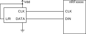

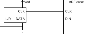

Note that in a single-microphone (mono) configuration, depending on the microphone’s implementation, either the left or the right channel (sampled at falling or rising CLK edge respectively) will contain reliable data.
If two microphones are used, one of them has to be set as left, the other as right (L/R pin tied high or to GND on the respective microphone). It is strongly recommended to use two microphones of exactly the same brand and type so that their timings in left and right operation match.
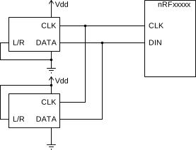

Pin configuration
The CLK and DIN signals associated to the PDM module are mapped to physical pins according to the configuration specified in the PSEL.CLK and PSEL.DIN registers respectively. If the CONNECT field in any PSEL register is set to Disconnected, the associated PDM module signal will not be connected to the required physical pins, and will not operate properly.
The PSEL.CLK and PSEL.DIN registers and their configurations are only used as long as the PDM module is enabled, and retained only as long as the device is in System ON mode. See POWER — Power supply for more information about power modes. When the peripheral is disabled, the pins will behave as regular GPIOs, and use the configuration in their respective OUT bit field and PIN_CNF[n] register.
To ensure correct behavior in the PDM module, the pins used by the PDM module must be configured in the GPIO peripheral as described in GPIO configuration before enabling peripheral before enabling the PDM module. This is to ensure that the pins used by the PDM module are driven correctly if the PDM module itself is temporarily disabled or the device temporarily enters System OFF. This configuration must be retained in the GPIO for the selected I/Os as long as the PDM module is supposed to be connected to an external PDM circuit.
Only one peripheral can be assigned to drive a particular GPIO pin at a time. Failing to do so may result in unpredictable behavior.
| PDM signal | PDM pin | Direction | Output value | Comment |
|---|---|---|---|---|
| CLK | As specified in PSEL.CLK | Output | 0 | |
| DIN | As specified in PSEL.DIN | Input | Not applicable |
Registers
Instances
| Instance | Base address | Description |
|---|---|---|
| PDM | 0x4001D000 | Pulse Density modulation (digital microphone) interface |
Register overview
| Register | Offset | Description |
|---|---|---|
| TASKS_START | 0x000 | Starts continuous PDM transfer |
| TASKS_STOP | 0x004 | Stops PDM transfer |
| EVENTS_STARTED | 0x100 | PDM transfer has started |
| EVENTS_STOPPED | 0x104 | PDM transfer has finished |
| EVENTS_END | 0x108 | The PDM has written the last sample specified by SAMPLE.MAXCNT (or the last sample after a STOP task has been received) to Data RAM |
| INTEN | 0x300 | Enable or disable interrupt |
| INTENSET | 0x304 | Enable interrupt |
| INTENCLR | 0x308 | Disable interrupt |
| ENABLE | 0x500 | PDM module enable register |
| PDMCLKCTRL | 0x504 | PDM clock generator control |
| MODE | 0x508 | Defines the routing of the connected PDM microphones' signals |
| GAINL | 0x518 | Left output gain adjustment |
| GAINR | 0x51C | Right output gain adjustment |
| RATIO | 0x520 | Selects the ratio between PDM_CLK and output sample rate. Change PDMCLKCTRL accordingly. |
| PSEL.CLK | 0x540 | Pin number configuration for PDM CLK signal |
| PSEL.DIN | 0x544 | Pin number configuration for PDM DIN signal |
| SAMPLE.PTR | 0x560 | RAM address pointer to write samples to with EasyDMA |
| SAMPLE.MAXCNT | 0x564 | Number of samples to allocate memory for in EasyDMA mode |
TASKS_START
Address offset: 0x000
Starts continuous PDM transfer
| Bit number | 31 | 30 | 29 | 28 | 27 | 26 | 25 | 24 | 23 | 22 | 21 | 20 | 19 | 18 | 17 | 16 | 15 | 14 | 13 | 12 | 11 | 10 | 9 | 8 | 7 | 6 | 5 | 4 | 3 | 2 | 1 | 0 | |||
|---|---|---|---|---|---|---|---|---|---|---|---|---|---|---|---|---|---|---|---|---|---|---|---|---|---|---|---|---|---|---|---|---|---|---|---|
| ID | A | ||||||||||||||||||||||||||||||||||
| Reset 0x00000000 | 0 | 0 | 0 | 0 | 0 | 0 | 0 | 0 | 0 | 0 | 0 | 0 | 0 | 0 | 0 | 0 | 0 | 0 | 0 | 0 | 0 | 0 | 0 | 0 | 0 | 0 | 0 | 0 | 0 | 0 | 0 | 0 | |||
| ID | R/W | Field | Value ID | Value | Description | ||||||||||||||||||||||||||||||
| A | W | TASKS_START | Starts continuous PDM transfer | ||||||||||||||||||||||||||||||||
Trigger | 1 | Trigger task | |||||||||||||||||||||||||||||||||
TASKS_STOP
Address offset: 0x004
Stops PDM transfer
| Bit number | 31 | 30 | 29 | 28 | 27 | 26 | 25 | 24 | 23 | 22 | 21 | 20 | 19 | 18 | 17 | 16 | 15 | 14 | 13 | 12 | 11 | 10 | 9 | 8 | 7 | 6 | 5 | 4 | 3 | 2 | 1 | 0 | |||
|---|---|---|---|---|---|---|---|---|---|---|---|---|---|---|---|---|---|---|---|---|---|---|---|---|---|---|---|---|---|---|---|---|---|---|---|
| ID | A | ||||||||||||||||||||||||||||||||||
| Reset 0x00000000 | 0 | 0 | 0 | 0 | 0 | 0 | 0 | 0 | 0 | 0 | 0 | 0 | 0 | 0 | 0 | 0 | 0 | 0 | 0 | 0 | 0 | 0 | 0 | 0 | 0 | 0 | 0 | 0 | 0 | 0 | 0 | 0 | |||
| ID | R/W | Field | Value ID | Value | Description | ||||||||||||||||||||||||||||||
| A | W | TASKS_STOP | Stops PDM transfer | ||||||||||||||||||||||||||||||||
Trigger | 1 | Trigger task | |||||||||||||||||||||||||||||||||
EVENTS_STARTED
Address offset: 0x100
PDM transfer has started
| Bit number | 31 | 30 | 29 | 28 | 27 | 26 | 25 | 24 | 23 | 22 | 21 | 20 | 19 | 18 | 17 | 16 | 15 | 14 | 13 | 12 | 11 | 10 | 9 | 8 | 7 | 6 | 5 | 4 | 3 | 2 | 1 | 0 | |||
|---|---|---|---|---|---|---|---|---|---|---|---|---|---|---|---|---|---|---|---|---|---|---|---|---|---|---|---|---|---|---|---|---|---|---|---|
| ID | A | ||||||||||||||||||||||||||||||||||
| Reset 0x00000000 | 0 | 0 | 0 | 0 | 0 | 0 | 0 | 0 | 0 | 0 | 0 | 0 | 0 | 0 | 0 | 0 | 0 | 0 | 0 | 0 | 0 | 0 | 0 | 0 | 0 | 0 | 0 | 0 | 0 | 0 | 0 | 0 | |||
| ID | R/W | Field | Value ID | Value | Description | ||||||||||||||||||||||||||||||
| A | RW | EVENTS_STARTED | PDM transfer has started | ||||||||||||||||||||||||||||||||
NotGenerated | 0 | Event not generated | |||||||||||||||||||||||||||||||||
Generated | 1 | Event generated | |||||||||||||||||||||||||||||||||
EVENTS_STOPPED
Address offset: 0x104
PDM transfer has finished
| Bit number | 31 | 30 | 29 | 28 | 27 | 26 | 25 | 24 | 23 | 22 | 21 | 20 | 19 | 18 | 17 | 16 | 15 | 14 | 13 | 12 | 11 | 10 | 9 | 8 | 7 | 6 | 5 | 4 | 3 | 2 | 1 | 0 | |||
|---|---|---|---|---|---|---|---|---|---|---|---|---|---|---|---|---|---|---|---|---|---|---|---|---|---|---|---|---|---|---|---|---|---|---|---|
| ID | A | ||||||||||||||||||||||||||||||||||
| Reset 0x00000000 | 0 | 0 | 0 | 0 | 0 | 0 | 0 | 0 | 0 | 0 | 0 | 0 | 0 | 0 | 0 | 0 | 0 | 0 | 0 | 0 | 0 | 0 | 0 | 0 | 0 | 0 | 0 | 0 | 0 | 0 | 0 | 0 | |||
| ID | R/W | Field | Value ID | Value | Description | ||||||||||||||||||||||||||||||
| A | RW | EVENTS_STOPPED | PDM transfer has finished | ||||||||||||||||||||||||||||||||
NotGenerated | 0 | Event not generated | |||||||||||||||||||||||||||||||||
Generated | 1 | Event generated | |||||||||||||||||||||||||||||||||
EVENTS_END
Address offset: 0x108
The PDM has written the last sample specified by SAMPLE.MAXCNT (or the last sample after a STOP task has been received) to Data RAM
| Bit number | 31 | 30 | 29 | 28 | 27 | 26 | 25 | 24 | 23 | 22 | 21 | 20 | 19 | 18 | 17 | 16 | 15 | 14 | 13 | 12 | 11 | 10 | 9 | 8 | 7 | 6 | 5 | 4 | 3 | 2 | 1 | 0 | |||
|---|---|---|---|---|---|---|---|---|---|---|---|---|---|---|---|---|---|---|---|---|---|---|---|---|---|---|---|---|---|---|---|---|---|---|---|
| ID | A | ||||||||||||||||||||||||||||||||||
| Reset 0x00000000 | 0 | 0 | 0 | 0 | 0 | 0 | 0 | 0 | 0 | 0 | 0 | 0 | 0 | 0 | 0 | 0 | 0 | 0 | 0 | 0 | 0 | 0 | 0 | 0 | 0 | 0 | 0 | 0 | 0 | 0 | 0 | 0 | |||
| ID | R/W | Field | Value ID | Value | Description | ||||||||||||||||||||||||||||||
| A | RW | EVENTS_END | The PDM has written the last sample specified by SAMPLE.MAXCNT (or the last sample after a STOP task has been received) to Data RAM | ||||||||||||||||||||||||||||||||
NotGenerated | 0 | Event not generated | |||||||||||||||||||||||||||||||||
Generated | 1 | Event generated | |||||||||||||||||||||||||||||||||
INTEN
Address offset: 0x300
Enable or disable interrupt
| Bit number | 31 | 30 | 29 | 28 | 27 | 26 | 25 | 24 | 23 | 22 | 21 | 20 | 19 | 18 | 17 | 16 | 15 | 14 | 13 | 12 | 11 | 10 | 9 | 8 | 7 | 6 | 5 | 4 | 3 | 2 | 1 | 0 | |||
|---|---|---|---|---|---|---|---|---|---|---|---|---|---|---|---|---|---|---|---|---|---|---|---|---|---|---|---|---|---|---|---|---|---|---|---|
| ID | C | B | A | ||||||||||||||||||||||||||||||||
| Reset 0x00000000 | 0 | 0 | 0 | 0 | 0 | 0 | 0 | 0 | 0 | 0 | 0 | 0 | 0 | 0 | 0 | 0 | 0 | 0 | 0 | 0 | 0 | 0 | 0 | 0 | 0 | 0 | 0 | 0 | 0 | 0 | 0 | 0 | |||
| ID | R/W | Field | Value ID | Value | Description | ||||||||||||||||||||||||||||||
| A | RW | STARTED | Enable or disable interrupt for event STARTED | ||||||||||||||||||||||||||||||||
Disabled | 0 | Disable | |||||||||||||||||||||||||||||||||
Enabled | 1 | Enable | |||||||||||||||||||||||||||||||||
| B | RW | STOPPED | Enable or disable interrupt for event STOPPED | ||||||||||||||||||||||||||||||||
Disabled | 0 | Disable | |||||||||||||||||||||||||||||||||
Enabled | 1 | Enable | |||||||||||||||||||||||||||||||||
| C | RW | END | Enable or disable interrupt for event END | ||||||||||||||||||||||||||||||||
Disabled | 0 | Disable | |||||||||||||||||||||||||||||||||
Enabled | 1 | Enable | |||||||||||||||||||||||||||||||||
INTENSET
Address offset: 0x304
Enable interrupt
| Bit number | 31 | 30 | 29 | 28 | 27 | 26 | 25 | 24 | 23 | 22 | 21 | 20 | 19 | 18 | 17 | 16 | 15 | 14 | 13 | 12 | 11 | 10 | 9 | 8 | 7 | 6 | 5 | 4 | 3 | 2 | 1 | 0 | |||
|---|---|---|---|---|---|---|---|---|---|---|---|---|---|---|---|---|---|---|---|---|---|---|---|---|---|---|---|---|---|---|---|---|---|---|---|
| ID | C | B | A | ||||||||||||||||||||||||||||||||
| Reset 0x00000000 | 0 | 0 | 0 | 0 | 0 | 0 | 0 | 0 | 0 | 0 | 0 | 0 | 0 | 0 | 0 | 0 | 0 | 0 | 0 | 0 | 0 | 0 | 0 | 0 | 0 | 0 | 0 | 0 | 0 | 0 | 0 | 0 | |||
| ID | R/W | Field | Value ID | Value | Description | ||||||||||||||||||||||||||||||
| A | RW | STARTED | Write '1' to enable interrupt for event STARTED | ||||||||||||||||||||||||||||||||
Set | 1 | Enable | |||||||||||||||||||||||||||||||||
Disabled | 0 | Read: Disabled | |||||||||||||||||||||||||||||||||
Enabled | 1 | Read: Enabled | |||||||||||||||||||||||||||||||||
| B | RW | STOPPED | Write '1' to enable interrupt for event STOPPED | ||||||||||||||||||||||||||||||||
Set | 1 | Enable | |||||||||||||||||||||||||||||||||
Disabled | 0 | Read: Disabled | |||||||||||||||||||||||||||||||||
Enabled | 1 | Read: Enabled | |||||||||||||||||||||||||||||||||
| C | RW | END | Write '1' to enable interrupt for event END | ||||||||||||||||||||||||||||||||
Set | 1 | Enable | |||||||||||||||||||||||||||||||||
Disabled | 0 | Read: Disabled | |||||||||||||||||||||||||||||||||
Enabled | 1 | Read: Enabled | |||||||||||||||||||||||||||||||||
INTENCLR
Address offset: 0x308
Disable interrupt
| Bit number | 31 | 30 | 29 | 28 | 27 | 26 | 25 | 24 | 23 | 22 | 21 | 20 | 19 | 18 | 17 | 16 | 15 | 14 | 13 | 12 | 11 | 10 | 9 | 8 | 7 | 6 | 5 | 4 | 3 | 2 | 1 | 0 | |||
|---|---|---|---|---|---|---|---|---|---|---|---|---|---|---|---|---|---|---|---|---|---|---|---|---|---|---|---|---|---|---|---|---|---|---|---|
| ID | C | B | A | ||||||||||||||||||||||||||||||||
| Reset 0x00000000 | 0 | 0 | 0 | 0 | 0 | 0 | 0 | 0 | 0 | 0 | 0 | 0 | 0 | 0 | 0 | 0 | 0 | 0 | 0 | 0 | 0 | 0 | 0 | 0 | 0 | 0 | 0 | 0 | 0 | 0 | 0 | 0 | |||
| ID | R/W | Field | Value ID | Value | Description | ||||||||||||||||||||||||||||||
| A | RW | STARTED | Write '1' to disable interrupt for event STARTED | ||||||||||||||||||||||||||||||||
Clear | 1 | Disable | |||||||||||||||||||||||||||||||||
Disabled | 0 | Read: Disabled | |||||||||||||||||||||||||||||||||
Enabled | 1 | Read: Enabled | |||||||||||||||||||||||||||||||||
| B | RW | STOPPED | Write '1' to disable interrupt for event STOPPED | ||||||||||||||||||||||||||||||||
Clear | 1 | Disable | |||||||||||||||||||||||||||||||||
Disabled | 0 | Read: Disabled | |||||||||||||||||||||||||||||||||
Enabled | 1 | Read: Enabled | |||||||||||||||||||||||||||||||||
| C | RW | END | Write '1' to disable interrupt for event END | ||||||||||||||||||||||||||||||||
Clear | 1 | Disable | |||||||||||||||||||||||||||||||||
Disabled | 0 | Read: Disabled | |||||||||||||||||||||||||||||||||
Enabled | 1 | Read: Enabled | |||||||||||||||||||||||||||||||||
ENABLE
Address offset: 0x500
PDM module enable register
| Bit number | 31 | 30 | 29 | 28 | 27 | 26 | 25 | 24 | 23 | 22 | 21 | 20 | 19 | 18 | 17 | 16 | 15 | 14 | 13 | 12 | 11 | 10 | 9 | 8 | 7 | 6 | 5 | 4 | 3 | 2 | 1 | 0 | |||
|---|---|---|---|---|---|---|---|---|---|---|---|---|---|---|---|---|---|---|---|---|---|---|---|---|---|---|---|---|---|---|---|---|---|---|---|
| ID | A | ||||||||||||||||||||||||||||||||||
| Reset 0x00000000 | 0 | 0 | 0 | 0 | 0 | 0 | 0 | 0 | 0 | 0 | 0 | 0 | 0 | 0 | 0 | 0 | 0 | 0 | 0 | 0 | 0 | 0 | 0 | 0 | 0 | 0 | 0 | 0 | 0 | 0 | 0 | 0 | |||
| ID | R/W | Field | Value ID | Value | Description | ||||||||||||||||||||||||||||||
| A | RW | ENABLE | Enable or disable PDM module | ||||||||||||||||||||||||||||||||
Disabled | 0 | Disable | |||||||||||||||||||||||||||||||||
Enabled | 1 | Enable | |||||||||||||||||||||||||||||||||
PDMCLKCTRL
Address offset: 0x504
PDM clock generator control
| Bit number | 31 | 30 | 29 | 28 | 27 | 26 | 25 | 24 | 23 | 22 | 21 | 20 | 19 | 18 | 17 | 16 | 15 | 14 | 13 | 12 | 11 | 10 | 9 | 8 | 7 | 6 | 5 | 4 | 3 | 2 | 1 | 0 | |||
|---|---|---|---|---|---|---|---|---|---|---|---|---|---|---|---|---|---|---|---|---|---|---|---|---|---|---|---|---|---|---|---|---|---|---|---|
| ID | A | A | A | A | A | A | A | A | A | A | A | A | A | A | A | A | A | A | A | A | A | A | A | A | A | A | A | A | A | A | A | A | |||
| Reset 0x08400000 | 0 | 0 | 0 | 0 | 1 | 0 | 0 | 0 | 0 | 1 | 0 | 0 | 0 | 0 | 0 | 0 | 0 | 0 | 0 | 0 | 0 | 0 | 0 | 0 | 0 | 0 | 0 | 0 | 0 | 0 | 0 | 0 | |||
| ID | R/W | Field | Value ID | Value | Description | ||||||||||||||||||||||||||||||
| A | RW | FREQ | PDM_CLK frequency configuration | ||||||||||||||||||||||||||||||||
1000K | 0x08000000 | PDM_CLK = 32 MHz / 32 = 1.000 MHz | |||||||||||||||||||||||||||||||||
Default | 0x08400000 | PDM_CLK = 32 MHz / 31 = 1.032 MHz. Nominal clock for RATIO=Ratio64. | |||||||||||||||||||||||||||||||||
1067K | 0x08800000 | PDM_CLK = 32 MHz / 30 = 1.067 MHz | |||||||||||||||||||||||||||||||||
1231K | 0x09800000 | PDM_CLK = 32 MHz / 26 = 1.231 MHz | |||||||||||||||||||||||||||||||||
1280K | 0x0A000000 | PDM_CLK = 32 MHz / 25 = 1.280 MHz. Nominal clock for RATIO=Ratio80. | |||||||||||||||||||||||||||||||||
1333K | 0x0A800000 | PDM_CLK = 32 MHz / 24 = 1.333 MHz | |||||||||||||||||||||||||||||||||
MODE
Address offset: 0x508
Defines the routing of the connected PDM microphones' signals
| Bit number | 31 | 30 | 29 | 28 | 27 | 26 | 25 | 24 | 23 | 22 | 21 | 20 | 19 | 18 | 17 | 16 | 15 | 14 | 13 | 12 | 11 | 10 | 9 | 8 | 7 | 6 | 5 | 4 | 3 | 2 | 1 | 0 | |||
|---|---|---|---|---|---|---|---|---|---|---|---|---|---|---|---|---|---|---|---|---|---|---|---|---|---|---|---|---|---|---|---|---|---|---|---|
| ID | B | A | |||||||||||||||||||||||||||||||||
| Reset 0x00000000 | 0 | 0 | 0 | 0 | 0 | 0 | 0 | 0 | 0 | 0 | 0 | 0 | 0 | 0 | 0 | 0 | 0 | 0 | 0 | 0 | 0 | 0 | 0 | 0 | 0 | 0 | 0 | 0 | 0 | 0 | 0 | 0 | |||
| ID | R/W | Field | Value ID | Value | Description | ||||||||||||||||||||||||||||||
| A | RW | OPERATION | Mono or stereo operation | ||||||||||||||||||||||||||||||||
Stereo | 0 | Sample and store one pair (left + right) of 16-bit samples per RAM word R=[31:16]; L=[15:0] | |||||||||||||||||||||||||||||||||
Mono | 1 | Sample and store two successive left samples (16 bits each) per RAM word L1=[31:16]; L0=[15:0] | |||||||||||||||||||||||||||||||||
| B | RW | EDGE | Defines on which PDM_CLK edge left (or mono) is sampled | ||||||||||||||||||||||||||||||||
LeftFalling | 0 | Left (or mono) is sampled on falling edge of PDM_CLK | |||||||||||||||||||||||||||||||||
LeftRising | 1 | Left (or mono) is sampled on rising edge of PDM_CLK | |||||||||||||||||||||||||||||||||
GAINL
Address offset: 0x518
Left output gain adjustment
| Bit number | 31 | 30 | 29 | 28 | 27 | 26 | 25 | 24 | 23 | 22 | 21 | 20 | 19 | 18 | 17 | 16 | 15 | 14 | 13 | 12 | 11 | 10 | 9 | 8 | 7 | 6 | 5 | 4 | 3 | 2 | 1 | 0 | |||
|---|---|---|---|---|---|---|---|---|---|---|---|---|---|---|---|---|---|---|---|---|---|---|---|---|---|---|---|---|---|---|---|---|---|---|---|
| ID | A | A | A | A | A | A | A | ||||||||||||||||||||||||||||
| Reset 0x00000028 | 0 | 0 | 0 | 0 | 0 | 0 | 0 | 0 | 0 | 0 | 0 | 0 | 0 | 0 | 0 | 0 | 0 | 0 | 0 | 0 | 0 | 0 | 0 | 0 | 0 | 0 | 1 | 0 | 1 | 0 | 0 | 0 | |||
| ID | R/W | Field | Value ID | Value | Description | ||||||||||||||||||||||||||||||
| A | RW | GAINL | Left output gain adjustment, in 0.5 dB steps, around the default module gain (see electrical parameters) 0x00 -20 dB gain adjust 0x01 -19.5 dB gain adjust (...) 0x27 -0.5 dB gain adjust 0x28 0 dB gain adjust 0x29 +0.5 dB gain adjust (...) 0x4F +19.5 dB gain adjust 0x50 +20 dB gain adjust | ||||||||||||||||||||||||||||||||
MinGain | 0x00 | -20 dB gain adjustment (minimum) | |||||||||||||||||||||||||||||||||
DefaultGain | 0x28 | 0 dB gain adjustment | |||||||||||||||||||||||||||||||||
MaxGain | 0x50 | +20 dB gain adjustment (maximum) | |||||||||||||||||||||||||||||||||
GAINR
Address offset: 0x51C
Right output gain adjustment
| Bit number | 31 | 30 | 29 | 28 | 27 | 26 | 25 | 24 | 23 | 22 | 21 | 20 | 19 | 18 | 17 | 16 | 15 | 14 | 13 | 12 | 11 | 10 | 9 | 8 | 7 | 6 | 5 | 4 | 3 | 2 | 1 | 0 | |||
|---|---|---|---|---|---|---|---|---|---|---|---|---|---|---|---|---|---|---|---|---|---|---|---|---|---|---|---|---|---|---|---|---|---|---|---|
| ID | A | A | A | A | A | A | A | ||||||||||||||||||||||||||||
| Reset 0x00000028 | 0 | 0 | 0 | 0 | 0 | 0 | 0 | 0 | 0 | 0 | 0 | 0 | 0 | 0 | 0 | 0 | 0 | 0 | 0 | 0 | 0 | 0 | 0 | 0 | 0 | 0 | 1 | 0 | 1 | 0 | 0 | 0 | |||
| ID | R/W | Field | Value ID | Value | Description | ||||||||||||||||||||||||||||||
| A | RW | GAINR | Right output gain adjustment, in 0.5 dB steps, around the default module gain (see electrical parameters) | ||||||||||||||||||||||||||||||||
MinGain | 0x00 | -20 dB gain adjustment (minimum) | |||||||||||||||||||||||||||||||||
DefaultGain | 0x28 | 0 dB gain adjustment | |||||||||||||||||||||||||||||||||
MaxGain | 0x50 | +20 dB gain adjustment (maximum) | |||||||||||||||||||||||||||||||||
RATIO
Address offset: 0x520
Selects the ratio between PDM_CLK and output sample rate. Change PDMCLKCTRL accordingly.
| Bit number | 31 | 30 | 29 | 28 | 27 | 26 | 25 | 24 | 23 | 22 | 21 | 20 | 19 | 18 | 17 | 16 | 15 | 14 | 13 | 12 | 11 | 10 | 9 | 8 | 7 | 6 | 5 | 4 | 3 | 2 | 1 | 0 | |||
|---|---|---|---|---|---|---|---|---|---|---|---|---|---|---|---|---|---|---|---|---|---|---|---|---|---|---|---|---|---|---|---|---|---|---|---|
| ID | A | ||||||||||||||||||||||||||||||||||
| Reset 0x00000000 | 0 | 0 | 0 | 0 | 0 | 0 | 0 | 0 | 0 | 0 | 0 | 0 | 0 | 0 | 0 | 0 | 0 | 0 | 0 | 0 | 0 | 0 | 0 | 0 | 0 | 0 | 0 | 0 | 0 | 0 | 0 | 0 | |||
| ID | R/W | Field | Value ID | Value | Description | ||||||||||||||||||||||||||||||
| A | RW | RATIO | Selects the ratio between PDM_CLK and output sample rate | ||||||||||||||||||||||||||||||||
Ratio64 | 0 | Ratio of 64 | |||||||||||||||||||||||||||||||||
Ratio80 | 1 | Ratio of 80 | |||||||||||||||||||||||||||||||||
PSEL.CLK
Address offset: 0x540
Pin number configuration for PDM CLK signal
| Bit number | 31 | 30 | 29 | 28 | 27 | 26 | 25 | 24 | 23 | 22 | 21 | 20 | 19 | 18 | 17 | 16 | 15 | 14 | 13 | 12 | 11 | 10 | 9 | 8 | 7 | 6 | 5 | 4 | 3 | 2 | 1 | 0 | |||
|---|---|---|---|---|---|---|---|---|---|---|---|---|---|---|---|---|---|---|---|---|---|---|---|---|---|---|---|---|---|---|---|---|---|---|---|
| ID | C | B | A | A | A | A | A | ||||||||||||||||||||||||||||
| Reset 0xFFFFFFFF | 1 | 1 | 1 | 1 | 1 | 1 | 1 | 1 | 1 | 1 | 1 | 1 | 1 | 1 | 1 | 1 | 1 | 1 | 1 | 1 | 1 | 1 | 1 | 1 | 1 | 1 | 1 | 1 | 1 | 1 | 1 | 1 | |||
| ID | R/W | Field | Value ID | Value | Description | ||||||||||||||||||||||||||||||
| A | RW | PIN | [0..31] | Pin number | |||||||||||||||||||||||||||||||
| B | RW | PORT | [0..1] | Port number | |||||||||||||||||||||||||||||||
| C | RW | CONNECT | Connection | ||||||||||||||||||||||||||||||||
Disconnected | 1 | Disconnect | |||||||||||||||||||||||||||||||||
Connected | 0 | Connect | |||||||||||||||||||||||||||||||||
PSEL.DIN
Address offset: 0x544
Pin number configuration for PDM DIN signal
| Bit number | 31 | 30 | 29 | 28 | 27 | 26 | 25 | 24 | 23 | 22 | 21 | 20 | 19 | 18 | 17 | 16 | 15 | 14 | 13 | 12 | 11 | 10 | 9 | 8 | 7 | 6 | 5 | 4 | 3 | 2 | 1 | 0 | |||
|---|---|---|---|---|---|---|---|---|---|---|---|---|---|---|---|---|---|---|---|---|---|---|---|---|---|---|---|---|---|---|---|---|---|---|---|
| ID | C | B | A | A | A | A | A | ||||||||||||||||||||||||||||
| Reset 0xFFFFFFFF | 1 | 1 | 1 | 1 | 1 | 1 | 1 | 1 | 1 | 1 | 1 | 1 | 1 | 1 | 1 | 1 | 1 | 1 | 1 | 1 | 1 | 1 | 1 | 1 | 1 | 1 | 1 | 1 | 1 | 1 | 1 | 1 | |||
| ID | R/W | Field | Value ID | Value | Description | ||||||||||||||||||||||||||||||
| A | RW | PIN | [0..31] | Pin number | |||||||||||||||||||||||||||||||
| B | RW | PORT | [0..1] | Port number | |||||||||||||||||||||||||||||||
| C | RW | CONNECT | Connection | ||||||||||||||||||||||||||||||||
Disconnected | 1 | Disconnect | |||||||||||||||||||||||||||||||||
Connected | 0 | Connect | |||||||||||||||||||||||||||||||||
SAMPLE.PTR
Address offset: 0x560
RAM address pointer to write samples to with EasyDMA
| Bit number | 31 | 30 | 29 | 28 | 27 | 26 | 25 | 24 | 23 | 22 | 21 | 20 | 19 | 18 | 17 | 16 | 15 | 14 | 13 | 12 | 11 | 10 | 9 | 8 | 7 | 6 | 5 | 4 | 3 | 2 | 1 | 0 | |||
|---|---|---|---|---|---|---|---|---|---|---|---|---|---|---|---|---|---|---|---|---|---|---|---|---|---|---|---|---|---|---|---|---|---|---|---|
| ID | A | A | A | A | A | A | A | A | A | A | A | A | A | A | A | A | A | A | A | A | A | A | A | A | A | A | A | A | A | A | A | A | |||
| Reset 0x00000000 | 0 | 0 | 0 | 0 | 0 | 0 | 0 | 0 | 0 | 0 | 0 | 0 | 0 | 0 | 0 | 0 | 0 | 0 | 0 | 0 | 0 | 0 | 0 | 0 | 0 | 0 | 0 | 0 | 0 | 0 | 0 | 0 | |||
| ID | R/W | Field | Value ID | Value | Description | ||||||||||||||||||||||||||||||
| A | RW | SAMPLEPTR | Address to write PDM samples to over DMA Note: See the memory chapter for details about which memories are available for EasyDMA. | ||||||||||||||||||||||||||||||||
SAMPLE.MAXCNT
Address offset: 0x564
Number of samples to allocate memory for in EasyDMA mode
| Bit number | 31 | 30 | 29 | 28 | 27 | 26 | 25 | 24 | 23 | 22 | 21 | 20 | 19 | 18 | 17 | 16 | 15 | 14 | 13 | 12 | 11 | 10 | 9 | 8 | 7 | 6 | 5 | 4 | 3 | 2 | 1 | 0 | |||
|---|---|---|---|---|---|---|---|---|---|---|---|---|---|---|---|---|---|---|---|---|---|---|---|---|---|---|---|---|---|---|---|---|---|---|---|
| ID | A | A | A | A | A | A | A | A | A | A | A | A | A | A | A | ||||||||||||||||||||
| Reset 0x00000000 | 0 | 0 | 0 | 0 | 0 | 0 | 0 | 0 | 0 | 0 | 0 | 0 | 0 | 0 | 0 | 0 | 0 | 0 | 0 | 0 | 0 | 0 | 0 | 0 | 0 | 0 | 0 | 0 | 0 | 0 | 0 | 0 | |||
| ID | R/W | Field | Value ID | Value | Description | ||||||||||||||||||||||||||||||
| A | RW | BUFFSIZE | [0..32767] | Length of DMA RAM allocation in number of samples | |||||||||||||||||||||||||||||||
Electrical specification
PDM Electrical Specification
| Symbol | Description | Min. | Typ. | Max. | Units |
|---|---|---|---|---|---|
| fPDM,CLK,64 | PDM clock speed. PDMCLKCTRL = Default (Setting needed for 16 MHz sample frequency @ RATIO = Ratio64) | 1.032 | MHz | ||
| fPDM,CLK,80 | PDM clock speed. PDMCLKCTRL = 1280K (Setting needed for 16 MHz sample frequency @ RATIO = Ratio80) | 1.280 | MHz | ||
| tPDM,JITTER | Jitter in PDM clock output | 20 | ns | ||
| TdPDM,CLK | PDM clock duty cycle | 40 | 50 | 60 | % |
| tPDM,DATA | Decimation filter delay | 5 | ms | ||
| tPDM,cv | Allowed clock edge to data valid | 125 | ns | ||
| tPDM,ci | Allowed (other) clock edge to data invalid | 0 | ns | ||
| tPDM,s | Data setup time at fPDM,CLK=1.024 MHz or 1.280 MHz | 65 | ns | ||
| tPDM,h | Data hold time at fPDM,CLK=1.024 MHz or 1.280 MHz | 0 | ns | ||
| GPDM,default | Default (reset) absolute gain of the PDM module | 3.2 | dB |