QDEC — Quadrature decoder
The Quadrature decoder (QDEC) provides buffered decoding of quadrature-encoded sensor signals. It is suitable for mechanical and optical sensors.
The sample period and accumulation are configurable to match application requirements. The QDEC provides the following:
- Digital waveform decoding from off-chip quadrature encoder
- Sample accumulation eliminating hard real-time requirements to be enforced on application
- Optional input de-bounce filters.
- Optional LED output signal for optical encoders
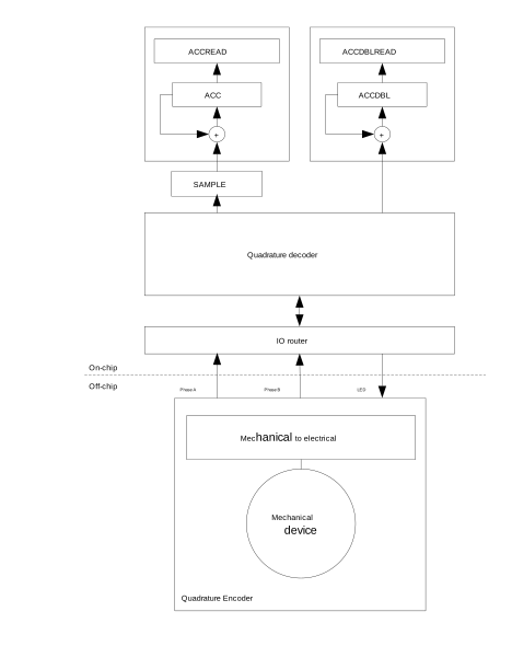
Sampling and decoding
The QDEC decodes the output from an incremental motion encoder by sampling the QDEC phase input pins (A and B).
The off-chip quadrature encoder is an incremental motion encoder outputting two waveforms, phase A and phase B. The two output waveforms are always 90 degrees out of phase, meaning that one always changes level before the other. The direction of movement is indicated by the waveform that changes level first. Invalid transitions may occur, meaning the two waveforms simultaneously switch. This may occur if the wheel rotates too fast relative to the sample rate set for the decoder.
The QDEC decodes the output from the off-chip encoder by sampling the QDEC phase input pins (A and B) at a fixed rate as specified in the SAMPLEPER register.
If the SAMPLEPER value needs to be changed, the QDEC shall be stopped using the STOP task. SAMPLEPER can be then changed upon receiving the STOPPED event, and QDEC can be restarted using the START task. Failing to do so may result in unpredictable behavior.
It is good practice to only change registers LEDPOL, REPORTPER, DBFEN, and LEDPRE when the QDEC is stopped.
When started, the decoder continuously samples the two input waveforms and decodes these by comparing the current sample pair (n) with the previous sample pair (n-1).
The decoding of the sample pairs is described in the table below.
| Previous sample pair(n - 1) | Current samples pair(n) | SAMPLE register | ACC operation | ACCDBL operation | Description | ||
|---|---|---|---|---|---|---|---|
| A | B | A | B | ||||
| 0 | 0 | 0 | 0 | 0 | No change | No change | No movement |
| 0 | 0 | 0 | 1 | 1 | Increment | No change | Movement in positive direction |
| 0 | 0 | 1 | 0 | -1 | Decrement | No change | Movement in negative direction |
| 0 | 0 | 1 | 1 | 2 | No change | Increment | Error: Double transition |
| 0 | 1 | 0 | 0 | -1 | Decrement | No change | Movement in negative direction |
| 0 | 1 | 0 | 1 | 0 | No change | No change | No movement |
| 0 | 1 | 1 | 0 | 2 | No change | Increment | Error: Double transition |
| 0 | 1 | 1 | 1 | 1 | Increment | No change | Movement in positive direction |
| 1 | 0 | 0 | 0 | 1 | Increment | No change | Movement in positive direction |
| 1 | 0 | 0 | 1 | 2 | No change | Increment | Error: Double transition |
| 1 | 0 | 1 | 0 | 0 | No change | No change | No movement |
| 1 | 0 | 1 | 1 | -1 | Decrement | No change | Movement in negative direction |
| 1 | 1 | 0 | 0 | 2 | No change | Increment | Error: Double transition |
| 1 | 1 | 0 | 1 | -1 | Decrement | No change | Movement in negative direction |
| 1 | 1 | 1 | 0 | 1 | Increment | No change | Movement in positive direction |
| 1 | 1 | 1 | 1 | 0 | No change | No change | No movement |
LED output
The LED output follows the sample period. The LED is switched on for a set period before sampling and then switched off immediately after. The period the LED is switched on before sampling is given in the LEDPRE register.
The LED output pin polarity is specified in the LEDPOL register.
When using off-chip mechanical encoders not requiring an LED, the LED output can be disabled by writing value 'Disconnected' to the CONNECT field of the PSEL.LED register. In this case, the QDEC will not acquire access to a pin for the LED output.
Debounce filters
Each of the two-phase inputs have digital debounce filters.
When enabled through the DBFEN register, the filter inputs are sampled at a fixed 1 MHz frequency during the entire sample period (which is specified in the SAMPLEPER register). The filters require all of the samples within this sample period to equal before the input signal is accepted and transferred to the output of the filter.
As a result, only input signal with a steady state longer than twice the period specified in SAMPLEPER are guaranteed to pass through the filter. Any signal with a steady state shorter than SAMPLEPER will always be suppressed by the filter. It is assumed that the frequency during the debounce period never exceeds 500 kHz (as required by the Nyquist theorem when using a 1 MHz sample frequency).
The LED will always be ON when the debounce filters are enabled, as the inputs in this case will be sampled continuously.
When the debounce filters are enabled, displacements reported by the QDEC peripheral are delayed by one SAMPLEPER period.
Accumulators
The quadrature decoder contains two accumulator registers, ACC and ACCDBL. These registers accumulate valid motion sample values and the number of detected invalid samples (double transitions), respectively.
The ACC register accumulates all valid values (1/-1) written to the SAMPLE register. This can be useful for preventing hard real-time requirements from being enforced on the application. When using the ACC register, the application can fetch data when necessary instead of reading all SAMPLE register output. The ACC register holds the relative movement of the external mechanical device from the previous clearing of the ACC register. Sample values indicating a double transition (2) will not be accumulated in the ACC register.
An ACCOF event is generated if the ACC receives a SAMPLE value that would cause the register to overflow or underflow. Any SAMPLE value that would cause an ACC overflow or underflow will be discarded, but any samples that do not cause the ACC to overflow or underflow will still be accepted.
The accumulator ACCDBL accumulates the number of detected double transitions since the previous clearing of the ACCDBL register.
The ACC and ACCDBL registers can be cleared by the READCLRACC and subsequently read using the ACCREAD and ACCDBLREAD registers.
The ACC register can be separately cleared by the RDCLRACC and subsequently read using the ACCREAD registers.
The ACCDBL register can be separately cleared by the RDCLRDBL and subsequently read using the ACCDBLREAD registers.
The REPORTPER register allows automated capture of multiple samples before sending an event. When a non-null displacement is captured and accumulated, a REPORTRDY event is sent. When one or more double-displacements are captured and accumulated, a DBLRDY event is sent. The REPORTPER field in this register determines how many samples must be accumulated before the contents are evaluated and a REPORTRDY or DBLRDY event is sent.
Using the RDCLRACC task (manually sent upon receiving the event, or using the DBLRDY_RDCLRACC shortcut), ACCREAD can then be read.
When a double transition has been captured and accumulated, a DBLRDY event is sent. Using the RDCLRDBL task (manually sent upon receiving the event, or using the DBLRDY_RDCLRDBL shortcut), ACCDBLREAD can then be read.
Output/input pins
The QDEC uses a three-pin interface to the off-chip quadrature encoder.
These pins are acquired when the QDEC is enabled in the ENABLE register. The pins acquired by the QDEC cannot be written by the CPU, but they can still be read by the CPU.
The pin numbers used for the QDEC are selected using the PSEL.n registers.
Pin configuration
The Phase A, Phase B, and LED signals are mapped to physical pins according to the configuration specified in the PSEL.A, PSEL.B, and PSEL.LED registers respectively.
If the CONNECT field value 'Disconnected' is specified in any of these registers, the associated signal will not be connected to any physical pin. The PSEL.A, PSEL.B, and PSEL.LED registers and their configurations are only used as long as the QDEC is enabled, and retained only as long as the device is in ON mode. When the peripheral is disabled, the pins will behave as regular GPIOs, and use the configuration in their respective OUT bit field and PIN_CNF[n] register.
To secure correct behavior in the QDEC, the pins used by the QDEC must be configured in the GPIO peripheral as described in GPIO configuration before enabling peripheral before enabling the QDEC. This configuration must be retained in the GPIO for the selected I/Os as long as the QDEC is enabled.
Only one peripheral can be assigned to drive a particular GPIO pin at a time. Failing to do so may result in unpredictable behavior.
| QDEC signal | QDEC pin | Direction | Output value | Comment |
|---|---|---|---|---|
| Phase A | As specified in PSEL.A | Input | Not applicable | |
| Phase B | As specified in PSEL.B | Input | Not applicable | |
| LED | As specified in PSEL.LED | Input | Not applicable |
Registers
Instances
| Instance | Base address | Description |
|---|---|---|
| QDEC | 0x40012000 | Quadrature decoder |
Register overview
| Register | Offset | Description |
|---|---|---|
| TASKS_START | 0x000 | Task starting the quadrature decoder |
| TASKS_STOP | 0x004 | Task stopping the quadrature decoder |
| TASKS_READCLRACC | 0x008 | Read and clear ACC and ACCDBL |
| TASKS_RDCLRACC | 0x00C | Read and clear ACC |
| TASKS_RDCLRDBL | 0x010 | Read and clear ACCDBL |
| EVENTS_SAMPLERDY | 0x100 | Event being generated for every new sample value written to the SAMPLE register |
| EVENTS_REPORTRDY | 0x104 | Non-null report ready |
| EVENTS_ACCOF | 0x108 | ACC or ACCDBL register overflow |
| EVENTS_DBLRDY | 0x10C | Double displacement(s) detected |
| EVENTS_STOPPED | 0x110 | QDEC has been stopped |
| SHORTS | 0x200 | Shortcuts between local events and tasks |
| INTENSET | 0x304 | Enable interrupt |
| INTENCLR | 0x308 | Disable interrupt |
| ENABLE | 0x500 | Enable the quadrature decoder |
| LEDPOL | 0x504 | LED output pin polarity |
| SAMPLEPER | 0x508 | Sample period |
| SAMPLE | 0x50C | Motion sample value |
| REPORTPER | 0x510 | Number of samples to be taken before REPORTRDY and DBLRDY events can be generated |
| ACC | 0x514 | Register accumulating the valid transitions |
| ACCREAD | 0x518 | Snapshot of the ACC register, updated by the READCLRACC or RDCLRACC task |
| PSEL.LED | 0x51C | Pin select for LED signal |
| PSEL.A | 0x520 | Pin select for A signal |
| PSEL.B | 0x524 | Pin select for B signal |
| DBFEN | 0x528 | Enable input debounce filters |
| LEDPRE | 0x540 | Time period the LED is switched ON prior to sampling |
| ACCDBL | 0x544 | Register accumulating the number of detected double transitions |
| ACCDBLREAD | 0x548 | Snapshot of the ACCDBL, updated by the READCLRACC or RDCLRDBL task |
TASKS_START
Address offset: 0x000
Task starting the quadrature decoder
When started, the SAMPLE register will be continuously updated at the rate given in the SAMPLEPER register.
| Bit number | 31 | 30 | 29 | 28 | 27 | 26 | 25 | 24 | 23 | 22 | 21 | 20 | 19 | 18 | 17 | 16 | 15 | 14 | 13 | 12 | 11 | 10 | 9 | 8 | 7 | 6 | 5 | 4 | 3 | 2 | 1 | 0 | |||
|---|---|---|---|---|---|---|---|---|---|---|---|---|---|---|---|---|---|---|---|---|---|---|---|---|---|---|---|---|---|---|---|---|---|---|---|
| ID | A | ||||||||||||||||||||||||||||||||||
| Reset 0x00000000 | 0 | 0 | 0 | 0 | 0 | 0 | 0 | 0 | 0 | 0 | 0 | 0 | 0 | 0 | 0 | 0 | 0 | 0 | 0 | 0 | 0 | 0 | 0 | 0 | 0 | 0 | 0 | 0 | 0 | 0 | 0 | 0 | |||
| ID | R/W | Field | Value ID | Value | Description | ||||||||||||||||||||||||||||||
| A | W | TASKS_START | Task starting the quadrature decoder When started, the SAMPLE register will be continuously updated at the rate given in the SAMPLEPER register. | ||||||||||||||||||||||||||||||||
Trigger | 1 | Trigger task | |||||||||||||||||||||||||||||||||
TASKS_STOP
Address offset: 0x004
Task stopping the quadrature decoder
| Bit number | 31 | 30 | 29 | 28 | 27 | 26 | 25 | 24 | 23 | 22 | 21 | 20 | 19 | 18 | 17 | 16 | 15 | 14 | 13 | 12 | 11 | 10 | 9 | 8 | 7 | 6 | 5 | 4 | 3 | 2 | 1 | 0 | |||
|---|---|---|---|---|---|---|---|---|---|---|---|---|---|---|---|---|---|---|---|---|---|---|---|---|---|---|---|---|---|---|---|---|---|---|---|
| ID | A | ||||||||||||||||||||||||||||||||||
| Reset 0x00000000 | 0 | 0 | 0 | 0 | 0 | 0 | 0 | 0 | 0 | 0 | 0 | 0 | 0 | 0 | 0 | 0 | 0 | 0 | 0 | 0 | 0 | 0 | 0 | 0 | 0 | 0 | 0 | 0 | 0 | 0 | 0 | 0 | |||
| ID | R/W | Field | Value ID | Value | Description | ||||||||||||||||||||||||||||||
| A | W | TASKS_STOP | Task stopping the quadrature decoder | ||||||||||||||||||||||||||||||||
Trigger | 1 | Trigger task | |||||||||||||||||||||||||||||||||
TASKS_READCLRACC
Address offset: 0x008
Read and clear ACC and ACCDBL
Task transferring the content of ACC to ACCREAD and the content of ACCDBL to ACCDBLREAD, and then clearing the ACC and ACCDBL registers. These read-and-clear operations will be done atomically.
| Bit number | 31 | 30 | 29 | 28 | 27 | 26 | 25 | 24 | 23 | 22 | 21 | 20 | 19 | 18 | 17 | 16 | 15 | 14 | 13 | 12 | 11 | 10 | 9 | 8 | 7 | 6 | 5 | 4 | 3 | 2 | 1 | 0 | |||
|---|---|---|---|---|---|---|---|---|---|---|---|---|---|---|---|---|---|---|---|---|---|---|---|---|---|---|---|---|---|---|---|---|---|---|---|
| ID | A | ||||||||||||||||||||||||||||||||||
| Reset 0x00000000 | 0 | 0 | 0 | 0 | 0 | 0 | 0 | 0 | 0 | 0 | 0 | 0 | 0 | 0 | 0 | 0 | 0 | 0 | 0 | 0 | 0 | 0 | 0 | 0 | 0 | 0 | 0 | 0 | 0 | 0 | 0 | 0 | |||
| ID | R/W | Field | Value ID | Value | Description | ||||||||||||||||||||||||||||||
| A | W | TASKS_READCLRACC | Read and clear ACC and ACCDBL Task transferring the content of ACC to ACCREAD and the content of ACCDBL to ACCDBLREAD, and then clearing the ACC and ACCDBL registers. These read-and-clear operations will be done atomically. | ||||||||||||||||||||||||||||||||
Trigger | 1 | Trigger task | |||||||||||||||||||||||||||||||||
TASKS_RDCLRACC
Address offset: 0x00C
Read and clear ACC
Task transferring the content of ACC to ACCREAD, and then clearing the ACC register. This read-and-clear operation will be done atomically.
| Bit number | 31 | 30 | 29 | 28 | 27 | 26 | 25 | 24 | 23 | 22 | 21 | 20 | 19 | 18 | 17 | 16 | 15 | 14 | 13 | 12 | 11 | 10 | 9 | 8 | 7 | 6 | 5 | 4 | 3 | 2 | 1 | 0 | |||
|---|---|---|---|---|---|---|---|---|---|---|---|---|---|---|---|---|---|---|---|---|---|---|---|---|---|---|---|---|---|---|---|---|---|---|---|
| ID | A | ||||||||||||||||||||||||||||||||||
| Reset 0x00000000 | 0 | 0 | 0 | 0 | 0 | 0 | 0 | 0 | 0 | 0 | 0 | 0 | 0 | 0 | 0 | 0 | 0 | 0 | 0 | 0 | 0 | 0 | 0 | 0 | 0 | 0 | 0 | 0 | 0 | 0 | 0 | 0 | |||
| ID | R/W | Field | Value ID | Value | Description | ||||||||||||||||||||||||||||||
| A | W | TASKS_RDCLRACC | Read and clear ACC Task transferring the content of ACC to ACCREAD, and then clearing the ACC register. This read-and-clear operation will be done atomically. | ||||||||||||||||||||||||||||||||
Trigger | 1 | Trigger task | |||||||||||||||||||||||||||||||||
TASKS_RDCLRDBL
Address offset: 0x010
Read and clear ACCDBL
Task transferring the content of ACCDBL to ACCDBLREAD, and then clearing the ACCDBL register. This read-and-clear operation will be done atomically.
| Bit number | 31 | 30 | 29 | 28 | 27 | 26 | 25 | 24 | 23 | 22 | 21 | 20 | 19 | 18 | 17 | 16 | 15 | 14 | 13 | 12 | 11 | 10 | 9 | 8 | 7 | 6 | 5 | 4 | 3 | 2 | 1 | 0 | |||
|---|---|---|---|---|---|---|---|---|---|---|---|---|---|---|---|---|---|---|---|---|---|---|---|---|---|---|---|---|---|---|---|---|---|---|---|
| ID | A | ||||||||||||||||||||||||||||||||||
| Reset 0x00000000 | 0 | 0 | 0 | 0 | 0 | 0 | 0 | 0 | 0 | 0 | 0 | 0 | 0 | 0 | 0 | 0 | 0 | 0 | 0 | 0 | 0 | 0 | 0 | 0 | 0 | 0 | 0 | 0 | 0 | 0 | 0 | 0 | |||
| ID | R/W | Field | Value ID | Value | Description | ||||||||||||||||||||||||||||||
| A | W | TASKS_RDCLRDBL | Read and clear ACCDBL Task transferring the content of ACCDBL to ACCDBLREAD, and then clearing the ACCDBL register. This read-and-clear operation will be done atomically. | ||||||||||||||||||||||||||||||||
Trigger | 1 | Trigger task | |||||||||||||||||||||||||||||||||
EVENTS_SAMPLERDY
Address offset: 0x100
Event being generated for every new sample value written to the SAMPLE register
| Bit number | 31 | 30 | 29 | 28 | 27 | 26 | 25 | 24 | 23 | 22 | 21 | 20 | 19 | 18 | 17 | 16 | 15 | 14 | 13 | 12 | 11 | 10 | 9 | 8 | 7 | 6 | 5 | 4 | 3 | 2 | 1 | 0 | |||
|---|---|---|---|---|---|---|---|---|---|---|---|---|---|---|---|---|---|---|---|---|---|---|---|---|---|---|---|---|---|---|---|---|---|---|---|
| ID | A | ||||||||||||||||||||||||||||||||||
| Reset 0x00000000 | 0 | 0 | 0 | 0 | 0 | 0 | 0 | 0 | 0 | 0 | 0 | 0 | 0 | 0 | 0 | 0 | 0 | 0 | 0 | 0 | 0 | 0 | 0 | 0 | 0 | 0 | 0 | 0 | 0 | 0 | 0 | 0 | |||
| ID | R/W | Field | Value ID | Value | Description | ||||||||||||||||||||||||||||||
| A | RW | EVENTS_SAMPLERDY | Event being generated for every new sample value written to the SAMPLE register | ||||||||||||||||||||||||||||||||
NotGenerated | 0 | Event not generated | |||||||||||||||||||||||||||||||||
Generated | 1 | Event generated | |||||||||||||||||||||||||||||||||
EVENTS_REPORTRDY
Address offset: 0x104
Non-null report ready
Event generated when REPORTPER number of samples has been accumulated in the ACC register and the content of the ACC register is not equal to 0. (Thus, this event is only generated if a motion is detected since the previous clearing of the ACC register).
| Bit number | 31 | 30 | 29 | 28 | 27 | 26 | 25 | 24 | 23 | 22 | 21 | 20 | 19 | 18 | 17 | 16 | 15 | 14 | 13 | 12 | 11 | 10 | 9 | 8 | 7 | 6 | 5 | 4 | 3 | 2 | 1 | 0 | |||
|---|---|---|---|---|---|---|---|---|---|---|---|---|---|---|---|---|---|---|---|---|---|---|---|---|---|---|---|---|---|---|---|---|---|---|---|
| ID | A | ||||||||||||||||||||||||||||||||||
| Reset 0x00000000 | 0 | 0 | 0 | 0 | 0 | 0 | 0 | 0 | 0 | 0 | 0 | 0 | 0 | 0 | 0 | 0 | 0 | 0 | 0 | 0 | 0 | 0 | 0 | 0 | 0 | 0 | 0 | 0 | 0 | 0 | 0 | 0 | |||
| ID | R/W | Field | Value ID | Value | Description | ||||||||||||||||||||||||||||||
| A | RW | EVENTS_REPORTRDY | Non-null report ready Event generated when REPORTPER number of samples has been accumulated in the ACC register and the content of the ACC register is not equal to 0. (Thus, this event is only generated if a motion is detected since the previous clearing of the ACC register). | ||||||||||||||||||||||||||||||||
NotGenerated | 0 | Event not generated | |||||||||||||||||||||||||||||||||
Generated | 1 | Event generated | |||||||||||||||||||||||||||||||||
EVENTS_ACCOF
Address offset: 0x108
ACC or ACCDBL register overflow
| Bit number | 31 | 30 | 29 | 28 | 27 | 26 | 25 | 24 | 23 | 22 | 21 | 20 | 19 | 18 | 17 | 16 | 15 | 14 | 13 | 12 | 11 | 10 | 9 | 8 | 7 | 6 | 5 | 4 | 3 | 2 | 1 | 0 | |||
|---|---|---|---|---|---|---|---|---|---|---|---|---|---|---|---|---|---|---|---|---|---|---|---|---|---|---|---|---|---|---|---|---|---|---|---|
| ID | A | ||||||||||||||||||||||||||||||||||
| Reset 0x00000000 | 0 | 0 | 0 | 0 | 0 | 0 | 0 | 0 | 0 | 0 | 0 | 0 | 0 | 0 | 0 | 0 | 0 | 0 | 0 | 0 | 0 | 0 | 0 | 0 | 0 | 0 | 0 | 0 | 0 | 0 | 0 | 0 | |||
| ID | R/W | Field | Value ID | Value | Description | ||||||||||||||||||||||||||||||
| A | RW | EVENTS_ACCOF | ACC or ACCDBL register overflow | ||||||||||||||||||||||||||||||||
NotGenerated | 0 | Event not generated | |||||||||||||||||||||||||||||||||
Generated | 1 | Event generated | |||||||||||||||||||||||||||||||||
EVENTS_DBLRDY
Address offset: 0x10C
Double displacement(s) detected
Event generated when REPORTPER number of samples has been accumulated and the content of the ACCDBL register is not equal to 0. (Thus, this event is only generated if a double transition is detected since the previous clearing of the ACCDBL register).
| Bit number | 31 | 30 | 29 | 28 | 27 | 26 | 25 | 24 | 23 | 22 | 21 | 20 | 19 | 18 | 17 | 16 | 15 | 14 | 13 | 12 | 11 | 10 | 9 | 8 | 7 | 6 | 5 | 4 | 3 | 2 | 1 | 0 | |||
|---|---|---|---|---|---|---|---|---|---|---|---|---|---|---|---|---|---|---|---|---|---|---|---|---|---|---|---|---|---|---|---|---|---|---|---|
| ID | A | ||||||||||||||||||||||||||||||||||
| Reset 0x00000000 | 0 | 0 | 0 | 0 | 0 | 0 | 0 | 0 | 0 | 0 | 0 | 0 | 0 | 0 | 0 | 0 | 0 | 0 | 0 | 0 | 0 | 0 | 0 | 0 | 0 | 0 | 0 | 0 | 0 | 0 | 0 | 0 | |||
| ID | R/W | Field | Value ID | Value | Description | ||||||||||||||||||||||||||||||
| A | RW | EVENTS_DBLRDY | Double displacement(s) detected Event generated when REPORTPER number of samples has been accumulated and the content of the ACCDBL register is not equal to 0. (Thus, this event is only generated if a double transition is detected since the previous clearing of the ACCDBL register). | ||||||||||||||||||||||||||||||||
NotGenerated | 0 | Event not generated | |||||||||||||||||||||||||||||||||
Generated | 1 | Event generated | |||||||||||||||||||||||||||||||||
EVENTS_STOPPED
Address offset: 0x110
QDEC has been stopped
| Bit number | 31 | 30 | 29 | 28 | 27 | 26 | 25 | 24 | 23 | 22 | 21 | 20 | 19 | 18 | 17 | 16 | 15 | 14 | 13 | 12 | 11 | 10 | 9 | 8 | 7 | 6 | 5 | 4 | 3 | 2 | 1 | 0 | |||
|---|---|---|---|---|---|---|---|---|---|---|---|---|---|---|---|---|---|---|---|---|---|---|---|---|---|---|---|---|---|---|---|---|---|---|---|
| ID | A | ||||||||||||||||||||||||||||||||||
| Reset 0x00000000 | 0 | 0 | 0 | 0 | 0 | 0 | 0 | 0 | 0 | 0 | 0 | 0 | 0 | 0 | 0 | 0 | 0 | 0 | 0 | 0 | 0 | 0 | 0 | 0 | 0 | 0 | 0 | 0 | 0 | 0 | 0 | 0 | |||
| ID | R/W | Field | Value ID | Value | Description | ||||||||||||||||||||||||||||||
| A | RW | EVENTS_STOPPED | QDEC has been stopped | ||||||||||||||||||||||||||||||||
NotGenerated | 0 | Event not generated | |||||||||||||||||||||||||||||||||
Generated | 1 | Event generated | |||||||||||||||||||||||||||||||||
SHORTS
Address offset: 0x200
Shortcuts between local events and tasks
| Bit number | 31 | 30 | 29 | 28 | 27 | 26 | 25 | 24 | 23 | 22 | 21 | 20 | 19 | 18 | 17 | 16 | 15 | 14 | 13 | 12 | 11 | 10 | 9 | 8 | 7 | 6 | 5 | 4 | 3 | 2 | 1 | 0 | |||
|---|---|---|---|---|---|---|---|---|---|---|---|---|---|---|---|---|---|---|---|---|---|---|---|---|---|---|---|---|---|---|---|---|---|---|---|
| ID | G | F | E | D | C | B | A | ||||||||||||||||||||||||||||
| Reset 0x00000000 | 0 | 0 | 0 | 0 | 0 | 0 | 0 | 0 | 0 | 0 | 0 | 0 | 0 | 0 | 0 | 0 | 0 | 0 | 0 | 0 | 0 | 0 | 0 | 0 | 0 | 0 | 0 | 0 | 0 | 0 | 0 | 0 | |||
| ID | R/W | Field | Value ID | Value | Description | ||||||||||||||||||||||||||||||
| A | RW | REPORTRDY_READCLRACC | Shortcut between event REPORTRDY and task READCLRACC | ||||||||||||||||||||||||||||||||
Disabled | 0 | Disable shortcut | |||||||||||||||||||||||||||||||||
Enabled | 1 | Enable shortcut | |||||||||||||||||||||||||||||||||
| B | RW | SAMPLERDY_STOP | |||||||||||||||||||||||||||||||||
Disabled | 0 | Disable shortcut | |||||||||||||||||||||||||||||||||
Enabled | 1 | Enable shortcut | |||||||||||||||||||||||||||||||||
| C | RW | REPORTRDY_RDCLRACC | |||||||||||||||||||||||||||||||||
Disabled | 0 | Disable shortcut | |||||||||||||||||||||||||||||||||
Enabled | 1 | Enable shortcut | |||||||||||||||||||||||||||||||||
| D | RW | REPORTRDY_STOP | |||||||||||||||||||||||||||||||||
Disabled | 0 | Disable shortcut | |||||||||||||||||||||||||||||||||
Enabled | 1 | Enable shortcut | |||||||||||||||||||||||||||||||||
| E | RW | DBLRDY_RDCLRDBL | |||||||||||||||||||||||||||||||||
Disabled | 0 | Disable shortcut | |||||||||||||||||||||||||||||||||
Enabled | 1 | Enable shortcut | |||||||||||||||||||||||||||||||||
| F | RW | DBLRDY_STOP | |||||||||||||||||||||||||||||||||
Disabled | 0 | Disable shortcut | |||||||||||||||||||||||||||||||||
Enabled | 1 | Enable shortcut | |||||||||||||||||||||||||||||||||
| G | RW | SAMPLERDY_READCLRACC | Shortcut between event SAMPLERDY and task READCLRACC | ||||||||||||||||||||||||||||||||
Disabled | 0 | Disable shortcut | |||||||||||||||||||||||||||||||||
Enabled | 1 | Enable shortcut | |||||||||||||||||||||||||||||||||
INTENSET
Address offset: 0x304
Enable interrupt
| Bit number | 31 | 30 | 29 | 28 | 27 | 26 | 25 | 24 | 23 | 22 | 21 | 20 | 19 | 18 | 17 | 16 | 15 | 14 | 13 | 12 | 11 | 10 | 9 | 8 | 7 | 6 | 5 | 4 | 3 | 2 | 1 | 0 | |||
|---|---|---|---|---|---|---|---|---|---|---|---|---|---|---|---|---|---|---|---|---|---|---|---|---|---|---|---|---|---|---|---|---|---|---|---|
| ID | E | D | C | B | A | ||||||||||||||||||||||||||||||
| Reset 0x00000000 | 0 | 0 | 0 | 0 | 0 | 0 | 0 | 0 | 0 | 0 | 0 | 0 | 0 | 0 | 0 | 0 | 0 | 0 | 0 | 0 | 0 | 0 | 0 | 0 | 0 | 0 | 0 | 0 | 0 | 0 | 0 | 0 | |||
| ID | R/W | Field | Value ID | Value | Description | ||||||||||||||||||||||||||||||
| A | RW | SAMPLERDY | Write '1' to enable interrupt for event SAMPLERDY | ||||||||||||||||||||||||||||||||
Set | 1 | Enable | |||||||||||||||||||||||||||||||||
Disabled | 0 | Read: Disabled | |||||||||||||||||||||||||||||||||
Enabled | 1 | Read: Enabled | |||||||||||||||||||||||||||||||||
| B | RW | REPORTRDY | Write '1' to enable interrupt for event REPORTRDY Event generated when REPORTPER number of samples has been accumulated in the ACC register and the content of the ACC register is not equal to 0. (Thus, this event is only generated if a motion is detected since the previous clearing of the ACC register). | ||||||||||||||||||||||||||||||||
Set | 1 | Enable | |||||||||||||||||||||||||||||||||
Disabled | 0 | Read: Disabled | |||||||||||||||||||||||||||||||||
Enabled | 1 | Read: Enabled | |||||||||||||||||||||||||||||||||
| C | RW | ACCOF | Write '1' to enable interrupt for event ACCOF | ||||||||||||||||||||||||||||||||
Set | 1 | Enable | |||||||||||||||||||||||||||||||||
Disabled | 0 | Read: Disabled | |||||||||||||||||||||||||||||||||
Enabled | 1 | Read: Enabled | |||||||||||||||||||||||||||||||||
| D | RW | DBLRDY | Write '1' to enable interrupt for event DBLRDY Event generated when REPORTPER number of samples has been accumulated and the content of the ACCDBL register is not equal to 0. (Thus, this event is only generated if a double transition is detected since the previous clearing of the ACCDBL register). | ||||||||||||||||||||||||||||||||
Set | 1 | Enable | |||||||||||||||||||||||||||||||||
Disabled | 0 | Read: Disabled | |||||||||||||||||||||||||||||||||
Enabled | 1 | Read: Enabled | |||||||||||||||||||||||||||||||||
| E | RW | STOPPED | Write '1' to enable interrupt for event STOPPED | ||||||||||||||||||||||||||||||||
Set | 1 | Enable | |||||||||||||||||||||||||||||||||
Disabled | 0 | Read: Disabled | |||||||||||||||||||||||||||||||||
Enabled | 1 | Read: Enabled | |||||||||||||||||||||||||||||||||
INTENCLR
Address offset: 0x308
Disable interrupt
| Bit number | 31 | 30 | 29 | 28 | 27 | 26 | 25 | 24 | 23 | 22 | 21 | 20 | 19 | 18 | 17 | 16 | 15 | 14 | 13 | 12 | 11 | 10 | 9 | 8 | 7 | 6 | 5 | 4 | 3 | 2 | 1 | 0 | |||
|---|---|---|---|---|---|---|---|---|---|---|---|---|---|---|---|---|---|---|---|---|---|---|---|---|---|---|---|---|---|---|---|---|---|---|---|
| ID | E | D | C | B | A | ||||||||||||||||||||||||||||||
| Reset 0x00000000 | 0 | 0 | 0 | 0 | 0 | 0 | 0 | 0 | 0 | 0 | 0 | 0 | 0 | 0 | 0 | 0 | 0 | 0 | 0 | 0 | 0 | 0 | 0 | 0 | 0 | 0 | 0 | 0 | 0 | 0 | 0 | 0 | |||
| ID | R/W | Field | Value ID | Value | Description | ||||||||||||||||||||||||||||||
| A | RW | SAMPLERDY | Write '1' to disable interrupt for event SAMPLERDY | ||||||||||||||||||||||||||||||||
Clear | 1 | Disable | |||||||||||||||||||||||||||||||||
Disabled | 0 | Read: Disabled | |||||||||||||||||||||||||||||||||
Enabled | 1 | Read: Enabled | |||||||||||||||||||||||||||||||||
| B | RW | REPORTRDY | Write '1' to disable interrupt for event REPORTRDY Event generated when REPORTPER number of samples has been accumulated in the ACC register and the content of the ACC register is not equal to 0. (Thus, this event is only generated if a motion is detected since the previous clearing of the ACC register). | ||||||||||||||||||||||||||||||||
Clear | 1 | Disable | |||||||||||||||||||||||||||||||||
Disabled | 0 | Read: Disabled | |||||||||||||||||||||||||||||||||
Enabled | 1 | Read: Enabled | |||||||||||||||||||||||||||||||||
| C | RW | ACCOF | Write '1' to disable interrupt for event ACCOF | ||||||||||||||||||||||||||||||||
Clear | 1 | Disable | |||||||||||||||||||||||||||||||||
Disabled | 0 | Read: Disabled | |||||||||||||||||||||||||||||||||
Enabled | 1 | Read: Enabled | |||||||||||||||||||||||||||||||||
| D | RW | DBLRDY | Write '1' to disable interrupt for event DBLRDY Event generated when REPORTPER number of samples has been accumulated and the content of the ACCDBL register is not equal to 0. (Thus, this event is only generated if a double transition is detected since the previous clearing of the ACCDBL register). | ||||||||||||||||||||||||||||||||
Clear | 1 | Disable | |||||||||||||||||||||||||||||||||
Disabled | 0 | Read: Disabled | |||||||||||||||||||||||||||||||||
Enabled | 1 | Read: Enabled | |||||||||||||||||||||||||||||||||
| E | RW | STOPPED | Write '1' to disable interrupt for event STOPPED | ||||||||||||||||||||||||||||||||
Clear | 1 | Disable | |||||||||||||||||||||||||||||||||
Disabled | 0 | Read: Disabled | |||||||||||||||||||||||||||||||||
Enabled | 1 | Read: Enabled | |||||||||||||||||||||||||||||||||
ENABLE
Address offset: 0x500
Enable the quadrature decoder
| Bit number | 31 | 30 | 29 | 28 | 27 | 26 | 25 | 24 | 23 | 22 | 21 | 20 | 19 | 18 | 17 | 16 | 15 | 14 | 13 | 12 | 11 | 10 | 9 | 8 | 7 | 6 | 5 | 4 | 3 | 2 | 1 | 0 | |||
|---|---|---|---|---|---|---|---|---|---|---|---|---|---|---|---|---|---|---|---|---|---|---|---|---|---|---|---|---|---|---|---|---|---|---|---|
| ID | A | ||||||||||||||||||||||||||||||||||
| Reset 0x00000000 | 0 | 0 | 0 | 0 | 0 | 0 | 0 | 0 | 0 | 0 | 0 | 0 | 0 | 0 | 0 | 0 | 0 | 0 | 0 | 0 | 0 | 0 | 0 | 0 | 0 | 0 | 0 | 0 | 0 | 0 | 0 | 0 | |||
| ID | R/W | Field | Value ID | Value | Description | ||||||||||||||||||||||||||||||
| A- | RW | ENABLE | Enable or disable the quadrature decoder When enabled the decoder pins will be active. When disabled the quadrature decoder pins are not active and can be used as GPIO . | ||||||||||||||||||||||||||||||||
Disabled | 0 | Disable | |||||||||||||||||||||||||||||||||
Enabled | 1 | Enable | |||||||||||||||||||||||||||||||||
LEDPOL
Address offset: 0x504
LED output pin polarity
| Bit number | 31 | 30 | 29 | 28 | 27 | 26 | 25 | 24 | 23 | 22 | 21 | 20 | 19 | 18 | 17 | 16 | 15 | 14 | 13 | 12 | 11 | 10 | 9 | 8 | 7 | 6 | 5 | 4 | 3 | 2 | 1 | 0 | |||
|---|---|---|---|---|---|---|---|---|---|---|---|---|---|---|---|---|---|---|---|---|---|---|---|---|---|---|---|---|---|---|---|---|---|---|---|
| ID | A | ||||||||||||||||||||||||||||||||||
| Reset 0x00000000 | 0 | 0 | 0 | 0 | 0 | 0 | 0 | 0 | 0 | 0 | 0 | 0 | 0 | 0 | 0 | 0 | 0 | 0 | 0 | 0 | 0 | 0 | 0 | 0 | 0 | 0 | 0 | 0 | 0 | 0 | 0 | 0 | |||
| ID | R/W | Field | Value ID | Value | Description | ||||||||||||||||||||||||||||||
| A | RW | LEDPOL | LED output pin polarity | ||||||||||||||||||||||||||||||||
ActiveLow | 0 | Led active on output pin low | |||||||||||||||||||||||||||||||||
ActiveHigh | 1 | Led active on output pin high | |||||||||||||||||||||||||||||||||
SAMPLEPER
Address offset: 0x508
Sample period
| Bit number | 31 | 30 | 29 | 28 | 27 | 26 | 25 | 24 | 23 | 22 | 21 | 20 | 19 | 18 | 17 | 16 | 15 | 14 | 13 | 12 | 11 | 10 | 9 | 8 | 7 | 6 | 5 | 4 | 3 | 2 | 1 | 0 | |||
|---|---|---|---|---|---|---|---|---|---|---|---|---|---|---|---|---|---|---|---|---|---|---|---|---|---|---|---|---|---|---|---|---|---|---|---|
| ID | A | A | A | A | |||||||||||||||||||||||||||||||
| Reset 0x00000000 | 0 | 0 | 0 | 0 | 0 | 0 | 0 | 0 | 0 | 0 | 0 | 0 | 0 | 0 | 0 | 0 | 0 | 0 | 0 | 0 | 0 | 0 | 0 | 0 | 0 | 0 | 0 | 0 | 0 | 0 | 0 | 0 | |||
| ID | R/W | Field | Value ID | Value | Description | ||||||||||||||||||||||||||||||
| A | RW | SAMPLEPER | Sample period. The SAMPLE register will be updated for every new sample | ||||||||||||||||||||||||||||||||
128us | 0 | 128 µs | |||||||||||||||||||||||||||||||||
256us | 1 | 256 µs | |||||||||||||||||||||||||||||||||
512us | 2 | 512 µs | |||||||||||||||||||||||||||||||||
1024us | 3 | 1024 µs | |||||||||||||||||||||||||||||||||
2048us | 4 | 2048 µs | |||||||||||||||||||||||||||||||||
4096us | 5 | 4096 µs | |||||||||||||||||||||||||||||||||
8192us | 6 | 8192 µs | |||||||||||||||||||||||||||||||||
16384us | 7 | 16384 µs | |||||||||||||||||||||||||||||||||
32ms | 8 | 32768 µs | |||||||||||||||||||||||||||||||||
65ms | 9 | 65536 µs | |||||||||||||||||||||||||||||||||
131ms | 10 | 131072 µs | |||||||||||||||||||||||||||||||||
SAMPLE
Address offset: 0x50C
Motion sample value
| Bit number | 31 | 30 | 29 | 28 | 27 | 26 | 25 | 24 | 23 | 22 | 21 | 20 | 19 | 18 | 17 | 16 | 15 | 14 | 13 | 12 | 11 | 10 | 9 | 8 | 7 | 6 | 5 | 4 | 3 | 2 | 1 | 0 | |||
|---|---|---|---|---|---|---|---|---|---|---|---|---|---|---|---|---|---|---|---|---|---|---|---|---|---|---|---|---|---|---|---|---|---|---|---|
| ID | A | A | A | A | A | A | A | A | A | A | A | A | A | A | A | A | A | A | A | A | A | A | A | A | A | A | A | A | A | A | A | A | |||
| Reset 0x00000000 | 0 | 0 | 0 | 0 | 0 | 0 | 0 | 0 | 0 | 0 | 0 | 0 | 0 | 0 | 0 | 0 | 0 | 0 | 0 | 0 | 0 | 0 | 0 | 0 | 0 | 0 | 0 | 0 | 0 | 0 | 0 | 0 | |||
| ID | R/W | Field | Value ID | Value | Description | ||||||||||||||||||||||||||||||
| A | R | SAMPLE | [-1..2] | Last motion sample The value is a 2's complement value, and the sign gives the direction of the motion. The value '2' indicates a double transition. | |||||||||||||||||||||||||||||||
REPORTPER
Address offset: 0x510
Number of samples to be taken before REPORTRDY and DBLRDY events can be generated
| Bit number | 31 | 30 | 29 | 28 | 27 | 26 | 25 | 24 | 23 | 22 | 21 | 20 | 19 | 18 | 17 | 16 | 15 | 14 | 13 | 12 | 11 | 10 | 9 | 8 | 7 | 6 | 5 | 4 | 3 | 2 | 1 | 0 | |||
|---|---|---|---|---|---|---|---|---|---|---|---|---|---|---|---|---|---|---|---|---|---|---|---|---|---|---|---|---|---|---|---|---|---|---|---|
| ID | A | A | A | A | |||||||||||||||||||||||||||||||
| Reset 0x00000000 | 0 | 0 | 0 | 0 | 0 | 0 | 0 | 0 | 0 | 0 | 0 | 0 | 0 | 0 | 0 | 0 | 0 | 0 | 0 | 0 | 0 | 0 | 0 | 0 | 0 | 0 | 0 | 0 | 0 | 0 | 0 | 0 | |||
| ID | R/W | Field | Value ID | Value | Description | ||||||||||||||||||||||||||||||
| A | RW | REPORTPER | Specifies the number of samples to be accumulated in the ACC register before the REPORTRDY and DBLRDY events can be generated. The report period in [µs] is given as: RPUS = SP * RP Where RPUS is the report period in [µs/report], SP is the sample period in [µs/sample] specified in SAMPLEPER, and RP is the report period in [samples/report] specified in REPORTPER . | ||||||||||||||||||||||||||||||||
10Smpl | 0 | 10 samples/report | |||||||||||||||||||||||||||||||||
40Smpl | 1 | 40 samples/report | |||||||||||||||||||||||||||||||||
80Smpl | 2 | 80 samples/report | |||||||||||||||||||||||||||||||||
120Smpl | 3 | 120 samples/report | |||||||||||||||||||||||||||||||||
160Smpl | 4 | 160 samples/report | |||||||||||||||||||||||||||||||||
200Smpl | 5 | 200 samples/report | |||||||||||||||||||||||||||||||||
240Smpl | 6 | 240 samples/report | |||||||||||||||||||||||||||||||||
280Smpl | 7 | 280 samples/report | |||||||||||||||||||||||||||||||||
1Smpl | 8 | 1 sample/report | |||||||||||||||||||||||||||||||||
ACC
Address offset: 0x514
Register accumulating the valid transitions
| Bit number | 31 | 30 | 29 | 28 | 27 | 26 | 25 | 24 | 23 | 22 | 21 | 20 | 19 | 18 | 17 | 16 | 15 | 14 | 13 | 12 | 11 | 10 | 9 | 8 | 7 | 6 | 5 | 4 | 3 | 2 | 1 | 0 | |||
|---|---|---|---|---|---|---|---|---|---|---|---|---|---|---|---|---|---|---|---|---|---|---|---|---|---|---|---|---|---|---|---|---|---|---|---|
| ID | A | A | A | A | A | A | A | A | A | A | A | A | A | A | A | A | A | A | A | A | A | A | A | A | A | A | A | A | A | A | A | A | |||
| Reset 0x00000000 | 0 | 0 | 0 | 0 | 0 | 0 | 0 | 0 | 0 | 0 | 0 | 0 | 0 | 0 | 0 | 0 | 0 | 0 | 0 | 0 | 0 | 0 | 0 | 0 | 0 | 0 | 0 | 0 | 0 | 0 | 0 | 0 | |||
| ID | R/W | Field | Value ID | Value | Description | ||||||||||||||||||||||||||||||
| A | R | ACC | [-1024..1023] | Register accumulating all valid samples (not double transition) read from the SAMPLE register. Double transitions ( SAMPLE = 2 ) will not be accumulated in this register. The value is a 32 bit 2's complement value. If a sample that would cause this register to overflow or underflow is received, the sample will be ignored and an overflow event ( ACCOF ) will be generated. The ACC register is cleared by triggering the READCLRACC or the RDCLRACC task. | |||||||||||||||||||||||||||||||
ACCREAD
Address offset: 0x518
Snapshot of the ACC register, updated by the READCLRACC or RDCLRACC task
| Bit number | 31 | 30 | 29 | 28 | 27 | 26 | 25 | 24 | 23 | 22 | 21 | 20 | 19 | 18 | 17 | 16 | 15 | 14 | 13 | 12 | 11 | 10 | 9 | 8 | 7 | 6 | 5 | 4 | 3 | 2 | 1 | 0 | |||
|---|---|---|---|---|---|---|---|---|---|---|---|---|---|---|---|---|---|---|---|---|---|---|---|---|---|---|---|---|---|---|---|---|---|---|---|
| ID | A | A | A | A | A | A | A | A | A | A | A | A | A | A | A | A | A | A | A | A | A | A | A | A | A | A | A | A | A | A | A | A | |||
| Reset 0x00000000 | 0 | 0 | 0 | 0 | 0 | 0 | 0 | 0 | 0 | 0 | 0 | 0 | 0 | 0 | 0 | 0 | 0 | 0 | 0 | 0 | 0 | 0 | 0 | 0 | 0 | 0 | 0 | 0 | 0 | 0 | 0 | 0 | |||
| ID | R/W | Field | Value ID | Value | Description | ||||||||||||||||||||||||||||||
| A | R | ACCREAD | [-1024..1023] | Snapshot of the ACC register. The ACCREAD register is updated when the READCLRACC or RDCLRACC task is triggered. | |||||||||||||||||||||||||||||||
PSEL.LED
Address offset: 0x51C
Pin select for LED signal
| Bit number | 31 | 30 | 29 | 28 | 27 | 26 | 25 | 24 | 23 | 22 | 21 | 20 | 19 | 18 | 17 | 16 | 15 | 14 | 13 | 12 | 11 | 10 | 9 | 8 | 7 | 6 | 5 | 4 | 3 | 2 | 1 | 0 | |||
|---|---|---|---|---|---|---|---|---|---|---|---|---|---|---|---|---|---|---|---|---|---|---|---|---|---|---|---|---|---|---|---|---|---|---|---|
| ID | C | B | A | A | A | A | A | ||||||||||||||||||||||||||||
| Reset 0xFFFFFFFF | 1 | 1 | 1 | 1 | 1 | 1 | 1 | 1 | 1 | 1 | 1 | 1 | 1 | 1 | 1 | 1 | 1 | 1 | 1 | 1 | 1 | 1 | 1 | 1 | 1 | 1 | 1 | 1 | 1 | 1 | 1 | 1 | |||
| ID | R/W | Field | Value ID | Value | Description | ||||||||||||||||||||||||||||||
| A | RW | PIN | [0..31] | Pin number | |||||||||||||||||||||||||||||||
| B | RW | PORT | [0..1] | Port number | |||||||||||||||||||||||||||||||
| C | RW | CONNECT | Connection | ||||||||||||||||||||||||||||||||
Disconnected | 1 | Disconnect | |||||||||||||||||||||||||||||||||
Connected | 0 | Connect | |||||||||||||||||||||||||||||||||
PSEL.A
Address offset: 0x520
Pin select for A signal
| Bit number | 31 | 30 | 29 | 28 | 27 | 26 | 25 | 24 | 23 | 22 | 21 | 20 | 19 | 18 | 17 | 16 | 15 | 14 | 13 | 12 | 11 | 10 | 9 | 8 | 7 | 6 | 5 | 4 | 3 | 2 | 1 | 0 | |||
|---|---|---|---|---|---|---|---|---|---|---|---|---|---|---|---|---|---|---|---|---|---|---|---|---|---|---|---|---|---|---|---|---|---|---|---|
| ID | C | B | A | A | A | A | A | ||||||||||||||||||||||||||||
| Reset 0xFFFFFFFF | 1 | 1 | 1 | 1 | 1 | 1 | 1 | 1 | 1 | 1 | 1 | 1 | 1 | 1 | 1 | 1 | 1 | 1 | 1 | 1 | 1 | 1 | 1 | 1 | 1 | 1 | 1 | 1 | 1 | 1 | 1 | 1 | |||
| ID | R/W | Field | Value ID | Value | Description | ||||||||||||||||||||||||||||||
| A | RW | PIN | [0..31] | Pin number | |||||||||||||||||||||||||||||||
| B | RW | PORT | [0..1] | Port number | |||||||||||||||||||||||||||||||
| C | RW | CONNECT | Connection | ||||||||||||||||||||||||||||||||
Disconnected | 1 | Disconnect | |||||||||||||||||||||||||||||||||
Connected | 0 | Connect | |||||||||||||||||||||||||||||||||
PSEL.B
Address offset: 0x524
Pin select for B signal
| Bit number | 31 | 30 | 29 | 28 | 27 | 26 | 25 | 24 | 23 | 22 | 21 | 20 | 19 | 18 | 17 | 16 | 15 | 14 | 13 | 12 | 11 | 10 | 9 | 8 | 7 | 6 | 5 | 4 | 3 | 2 | 1 | 0 | |||
|---|---|---|---|---|---|---|---|---|---|---|---|---|---|---|---|---|---|---|---|---|---|---|---|---|---|---|---|---|---|---|---|---|---|---|---|
| ID | C | B | A | A | A | A | A | ||||||||||||||||||||||||||||
| Reset 0xFFFFFFFF | 1 | 1 | 1 | 1 | 1 | 1 | 1 | 1 | 1 | 1 | 1 | 1 | 1 | 1 | 1 | 1 | 1 | 1 | 1 | 1 | 1 | 1 | 1 | 1 | 1 | 1 | 1 | 1 | 1 | 1 | 1 | 1 | |||
| ID | R/W | Field | Value ID | Value | Description | ||||||||||||||||||||||||||||||
| A | RW | PIN | [0..31] | Pin number | |||||||||||||||||||||||||||||||
| B | RW | PORT | [0..1] | Port number | |||||||||||||||||||||||||||||||
| C | RW | CONNECT | Connection | ||||||||||||||||||||||||||||||||
Disconnected | 1 | Disconnect | |||||||||||||||||||||||||||||||||
Connected | 0 | Connect | |||||||||||||||||||||||||||||||||
DBFEN
Address offset: 0x528
Enable input debounce filters
| Bit number | 31 | 30 | 29 | 28 | 27 | 26 | 25 | 24 | 23 | 22 | 21 | 20 | 19 | 18 | 17 | 16 | 15 | 14 | 13 | 12 | 11 | 10 | 9 | 8 | 7 | 6 | 5 | 4 | 3 | 2 | 1 | 0 | |||
|---|---|---|---|---|---|---|---|---|---|---|---|---|---|---|---|---|---|---|---|---|---|---|---|---|---|---|---|---|---|---|---|---|---|---|---|
| ID | A | ||||||||||||||||||||||||||||||||||
| Reset 0x00000000 | 0 | 0 | 0 | 0 | 0 | 0 | 0 | 0 | 0 | 0 | 0 | 0 | 0 | 0 | 0 | 0 | 0 | 0 | 0 | 0 | 0 | 0 | 0 | 0 | 0 | 0 | 0 | 0 | 0 | 0 | 0 | 0 | |||
| ID | R/W | Field | Value ID | Value | Description | ||||||||||||||||||||||||||||||
| A | RW | DBFEN | Enable input debounce filters | ||||||||||||||||||||||||||||||||
Disabled | 0 | Debounce input filters disabled | |||||||||||||||||||||||||||||||||
Enabled | 1 | Debounce input filters enabled | |||||||||||||||||||||||||||||||||
LEDPRE
Address offset: 0x540
Time period the LED is switched ON prior to sampling
| Bit number | 31 | 30 | 29 | 28 | 27 | 26 | 25 | 24 | 23 | 22 | 21 | 20 | 19 | 18 | 17 | 16 | 15 | 14 | 13 | 12 | 11 | 10 | 9 | 8 | 7 | 6 | 5 | 4 | 3 | 2 | 1 | 0 | |||
|---|---|---|---|---|---|---|---|---|---|---|---|---|---|---|---|---|---|---|---|---|---|---|---|---|---|---|---|---|---|---|---|---|---|---|---|
| ID | A | A | A | A | A | A | A | A | A | ||||||||||||||||||||||||||
| Reset 0x00000010 | 0 | 0 | 0 | 0 | 0 | 0 | 0 | 0 | 0 | 0 | 0 | 0 | 0 | 0 | 0 | 0 | 0 | 0 | 0 | 0 | 0 | 0 | 0 | 0 | 0 | 0 | 0 | 1 | 0 | 0 | 0 | 0 | |||
| ID | R/W | Field | Value ID | Value | Description | ||||||||||||||||||||||||||||||
| A | RW | LEDPRE | [1..511] | Period in µs the LED is switched on prior to sampling | |||||||||||||||||||||||||||||||
ACCDBL
Address offset: 0x544
Register accumulating the number of detected double transitions
| Bit number | 31 | 30 | 29 | 28 | 27 | 26 | 25 | 24 | 23 | 22 | 21 | 20 | 19 | 18 | 17 | 16 | 15 | 14 | 13 | 12 | 11 | 10 | 9 | 8 | 7 | 6 | 5 | 4 | 3 | 2 | 1 | 0 | |||
|---|---|---|---|---|---|---|---|---|---|---|---|---|---|---|---|---|---|---|---|---|---|---|---|---|---|---|---|---|---|---|---|---|---|---|---|
| ID | A | A | A | A | |||||||||||||||||||||||||||||||
| Reset 0x00000000 | 0 | 0 | 0 | 0 | 0 | 0 | 0 | 0 | 0 | 0 | 0 | 0 | 0 | 0 | 0 | 0 | 0 | 0 | 0 | 0 | 0 | 0 | 0 | 0 | 0 | 0 | 0 | 0 | 0 | 0 | 0 | 0 | |||
| ID | R/W | Field | Value ID | Value | Description | ||||||||||||||||||||||||||||||
| A | R | ACCDBL | [0..15] | Register accumulating the number of detected double or illegal transitions. ( SAMPLE = 2 ). When this register has reached its maximum value, the accumulation of double/illegal transitions will stop. An overflow event (ACCOF) will be generated if any double or illegal transitions are detected after the maximum value was reached. This field is cleared by triggering the READCLRACC or RDCLRDBL task. | |||||||||||||||||||||||||||||||
ACCDBLREAD
Address offset: 0x548
Snapshot of the ACCDBL, updated by the READCLRACC or RDCLRDBL task
| Bit number | 31 | 30 | 29 | 28 | 27 | 26 | 25 | 24 | 23 | 22 | 21 | 20 | 19 | 18 | 17 | 16 | 15 | 14 | 13 | 12 | 11 | 10 | 9 | 8 | 7 | 6 | 5 | 4 | 3 | 2 | 1 | 0 | |||
|---|---|---|---|---|---|---|---|---|---|---|---|---|---|---|---|---|---|---|---|---|---|---|---|---|---|---|---|---|---|---|---|---|---|---|---|
| ID | A | A | A | A | |||||||||||||||||||||||||||||||
| Reset 0x00000000 | 0 | 0 | 0 | 0 | 0 | 0 | 0 | 0 | 0 | 0 | 0 | 0 | 0 | 0 | 0 | 0 | 0 | 0 | 0 | 0 | 0 | 0 | 0 | 0 | 0 | 0 | 0 | 0 | 0 | 0 | 0 | 0 | |||
| ID | R/W | Field | Value ID | Value | Description | ||||||||||||||||||||||||||||||
| A | R | ACCDBLREAD | [0..15] | Snapshot of the ACCDBL register. This field is updated when the READCLRACC or RDCLRDBL task is triggered. | |||||||||||||||||||||||||||||||
Electrical specification
QDEC Electrical Specification
| Symbol | Description | Min. | Typ. | Max. | Units |
|---|---|---|---|---|---|
| tSAMPLE | Time between sampling signals from quadrature decoder | 128 | 131072 | µs | |
| tLED | Time from LED is turned on to signals are sampled | 0 | 511 | µs |