Reference circuitry
To ensure good RF performance when designing PCBs, it is highly recommended to use the PCB layouts and component values provided by Nordic Semiconductor.
Documentation for the different package reference circuits, including Altium Designer files, PCB layout files, and PCB production files can be downloaded from the product page for the nRF52840 on www.nordicsemi.com.
In this section there are reference circuits for QIAA aQFN73™, QFAA QFN48, and CKAA WLCSP showing the components and component values to support on-chip features in a design.
- External supply from VDD is only available when power is supplied to VDDH. External supply is annotated with the VEXT net name.
- When supplying power from a USB source only, VBUS must be connected to VDDH if USB is to be used.
- Components required for DC/DC function are only needed if DC/DC mode is enabled for that regulator.
- NFC can be used in any configuration.
- USB can be used in any configuration as long as VBUS is supplied by the USB host.
- The schematics include an optional series resistor on the USB supply for improved immunity to transient overvoltage during VBUS connection. Using the series resistor is recommended for new designs.
- Two component values for the RF-Match network for the QIAA aQFN73 package are given and referred to as v1.0 and v1.1 in the following tables. The reference schematics use v1.1 component values, which are recommended for new designs to improve the margin for spurious emissions during regulatory approval tests. However, both v1.0 and v1.1 are valid and can be used. All other RF parameters are unchanged.
- A new reference design with four-component RF match has been added for the QIAA aQFN™73 package. The four-component RF match improves harmonic suppression when using Radio with TXPOWER equal to 5dBm or above. However, previous 3 component RF-match designs are valid and can be used. Using this four-component RF match is recommended for new designs.
Circuit configurations for QIAA aQFN73
| Config no. | Supply configuration | Features that can be enabled for each configuration example | |||||
|---|---|---|---|---|---|---|---|
| VDDH | VDD | EXTSUPPLY | DCDCEN0 | DCDCEN1 | USB | NFC | |
| Config. 1 | USB (VDDH = VBUS) | N/A | Yes | No | No | Yes | No |
| Config. 2 | Battery/Ext. regulator | N/A | Yes | No | No | Yes | No |
| Config. 3 | N/A | Battery/Ext. regulator | No | No | No | Yes | No |
| Config. 4 | Battery/Ext. regulator | N/A | Yes | Yes | Yes | Yes | No |
| Config. 5 | N/A | Battery/Ext. regulator | No | No | Yes | Yes | Yes |
| Config. 6 | N/A | Battery/Ext. regulator | No | No | No | No | No |
| Config. 71 | Battery/Ext. regulator | N/A | Yes | Yes | Yes | Yes | No |
1Reference design with four-component RF match.
Circuit configurations for QFAA QFN48
| Config no. | Supply configuration | Features that can be enabled for each configuration example | |||||
|---|---|---|---|---|---|---|---|
| VDDH1 | VDD | EXTSUPPLY2 | DCDCEN03 | DCDCEN1 | USB4 | NFC | |
| Config. 1 | N/A | Battery/Ext. regulator | N/A | N/A | Yes | N/A | No |
1High Voltage supply mode cannot be used because the VDDH pin is not routed in the QFN48 package.
2The external supply feature cannot be used because the VDDH pin is not routed in the QFN48 package.
3DCDC for REG0 stage cannot be used because the VDDH pin is not routed in the QFN48 package.
4USBD cannot be used because the USB pins are not routed in the QFN48 package.
Circuit configurations for CKAA WLCSP
| Config no. | Supply configuration | Features that can be enabled for each configuration example | |||||
|---|---|---|---|---|---|---|---|
| VDDH | VDD | EXTSUPPLY | DCDCEN0 | DCDCEN1 | USB | NFC | |
| Config. 1 | USB (VDDH = VBUS) | N/A | Yes | No | No | Yes | No |
| Config. 2 | Battery/Ext. regulator | N/A | Yes | No | No | Yes | No |
| Config. 3 | N/A | Battery/Ext. regulator | No | No | No | Yes | No |
| Config. 4 | Battery/Ext. regulator | N/A | Yes | Yes | Yes | Yes | No |
| Config. 5 | N/A | Battery/Ext. regulator | No | No | Yes | Yes | Yes |
| Config. 6 | N/A | Battery/Ext. regulator | No | No | No | No | No |
Circuit configuration no. 1 for QIAA aQFN73
Circuit configuration number 1 for QIAA aQFN73, showing the schematic and the bill of materials.
| Config no. | Supply configuration | Enabled features | |||||
|---|---|---|---|---|---|---|---|
| VDDH | VDD | EXTSUPPLY | DCDCEN0 | DCDCEN1 | USB | NFC | |
| Config. 1 | USB (VDDH = VBUS) | N/A | Yes | No | No | Yes | No |
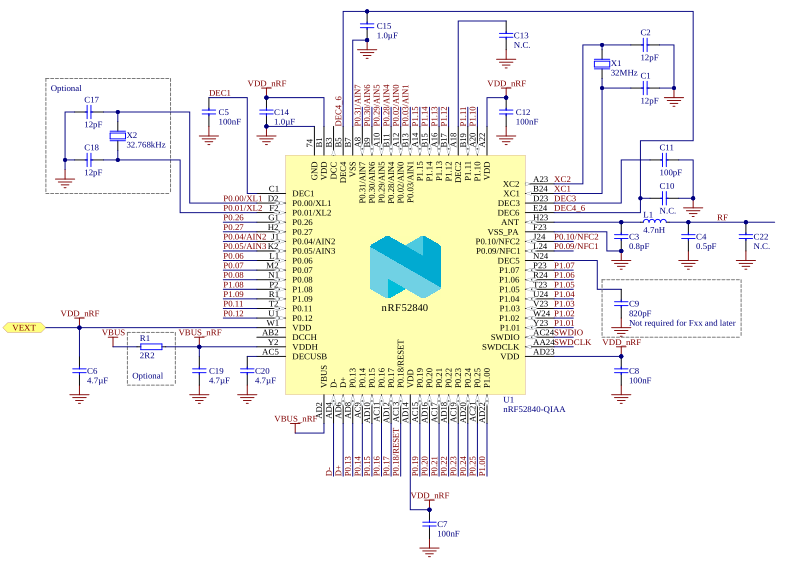
| Designator | Value v1.0 | Value v1.1 | Description | Footprint |
|---|---|---|---|---|
| C1, C2, C17, C18 | 12 pF | Capacitor, NP0, ±2% | 0402 | |
| C3 | 1 pF | 0.8 pF | Capacitor, NP0, ±10% | 0402 |
| C4 | 1 pF | 0.5 pF | Capacitor, NP0, ±10% | 0402 |
| C5, C7, C8, C12 | 100 nF | Capacitor, X7R, ±10% | 0402 | |
| C6, C20 | 4.7 µF | Capacitor, X7R, ±10% | 0603 | |
| C9 | 820 pF | Capacitor, NP0, ±5% Not required for Fxx and later | 0402 | |
| C10, C13, C22 | N.C. | Not mounted | 0402 | |
| C11 | 100 pF | Capacitor, NP0, ±5% | 0402 | |
| C14, C15 | 1.0 µF | Capacitor, X7R, ±10% | 0603 | |
| C19 | 4.7 µF | Capacitor, X7S, ±10% | 0603 | |
| L1 | 3.9 nH | 4.7 nH | High frequency chip inductor ±5% | 0402 |
| R1 | 2R2 | Resistor ±1%, 0.063W | 0402 | |
| U1 | nRF52840-QIAA | Multiprotocol Bluetooth® low energy, IEEE 802.15.4, ANT, and 2.4 GHz proprietary System on Chip | AQFN-73 | |
| X1 | 32 MHz | XTAL SMD 2016, 32 MHz, Cl=8 pF, Total Tol: ±40 ppm | XTAL_2016 | |
| X2 | 32.768 kHz | XTAL SMD 3215, 32.768 kHz, Cl=9 pF, Total Tol: ±50 ppm | XTAL_3215 | |
Circuit configuration no. 2 for QIAA aQFN73
Circuit configuration number 2 for QIAA aQFN73, showing the schematic and the bill of materials.
| Config no. | Supply configuration | Enabled features | |||||
|---|---|---|---|---|---|---|---|
| VDDH | VDD | EXTSUPPLY | DCDCEN0 | DCDCEN1 | USB | NFC | |
| Config. 2 | Battery/Ext. regulator | N/A | Yes | No | No | Yes | No |
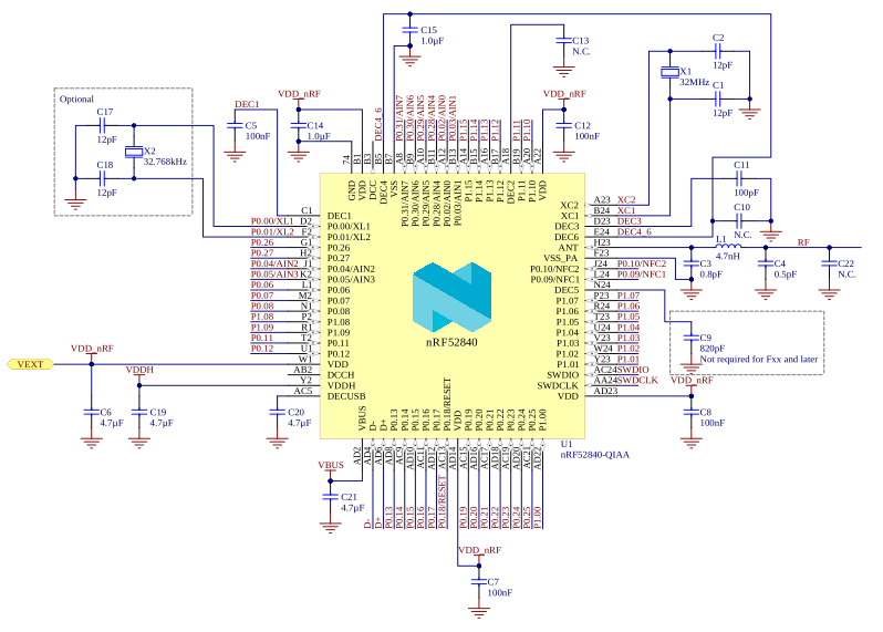
| Designator | Value v1.0 | Value v1.1 | Description | Footprint |
|---|---|---|---|---|
| C1, C2, C17, C18 | 12 pF | Capacitor, NP0, ±2% | 0402 | |
| C3 | 1 pF | 0.8 pF | Capacitor, NP0, ±10% | 0402 |
| C4 | 1 pF | 0.5 pF | Capacitor, NP0, ±10% | 0402 |
| C5, C7, C8, C12 | 100 nF | Capacitor, X7R, ±10% | 0402 | |
| C6, C20 | 4.7 µF | Capacitor, X7R, ±10% | 0603 | |
| C9 | 820 pF | Capacitor, NP0, ±5% Not required for Fxx and later | 0402 | |
| C10, C13, C22 | N.C. | Not mounted | 0402 | |
| C11 | 100 pF | Capacitor, NP0, ±5% | 0402 | |
| C14, C15 | 1.0 µF | Capacitor, X7R, ±10% | 0603 | |
| C19, C21 | 4.7 µF | Capacitor, X7S, ±10% | 0603 | |
| L1 | 3.9 nH | 4.7 nH | High frequency chip inductor ±5% | 0402 |
| U1 | nRF52840-QIAA | Multiprotocol Bluetooth low energy, IEEE 802.15.4, ANT, and 2.4 GHz proprietary System on Chip | AQFN-73 | |
| X1 | 32 MHz | XTAL SMD 2016, 32 MHz, Cl=8 pF, Total Tol: ±40 ppm | XTAL_2016 | |
| X2 | 32.768 kHz | XTAL SMD 3215, 32.768 kHz, Cl=9 pF, Total Tol: ±50 ppm | XTAL_3215 | |
Circuit configuration no. 3 for QIAA aQFN73
Circuit configuration number 3 for QIAA aQFN73, showing the schematic and the bill of materials.
| Config no. | Supply configuration | Enabled features | |||||
|---|---|---|---|---|---|---|---|
| VDDH | VDD | EXTSUPPLY | DCDCEN0 | DCDCEN1 | USB | NFC | |
| Config. 3 | N/A | Battery/Ext. regulator | No | No | No | Yes | No |
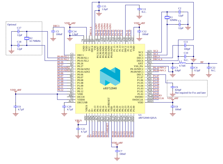
| Designator | Value v1.0 | Value v1.1 | Description | Footprint |
|---|---|---|---|---|
| C1, C2, C17, C18 | 12 pF | Capacitor, NP0, ±2% | 0402 | |
| C3 | 1 pF | 0.8 pF | Capacitor, NP0, ±10% | 0402 |
| C4 | 1 pF | 0.5 pF | Capacitor, NP0, ±10% | 0402 |
| C5, C7, C8, C12 | 100 nF | Capacitor, X7R, ±10% | 0402 | |
| C6, C20 | 4.7 µF | Capacitor, X7R, ±10% | 0603 | |
| C9 | 820 pF | Capacitor, NP0, ±5% Not required for Fxx and later | 0402 | |
| C10, C13, C22 | N.C. | Not mounted | 0402 | |
| C11 | 100 pF | Capacitor, NP0, ±5% | 0402 | |
| C14, C15 | 1.0 µF | Capacitor, X7R, ±10% | 0603 | |
| C21 | 4.7 µF | Capacitor, X7S, ±10% | 0603 | |
| L1 | 3.9 nH | 4.7 nH | High frequency chip inductor ±5% | 0402 |
| U1 | nRF52840-QIAA | Multiprotocol Bluetooth low energy, IEEE 802.15.4, ANT, and 2.4 GHz proprietary System on Chip | AQFN-73 | |
| X1 | 32 MHz | XTAL SMD 2016, 32 MHz, Cl=8 pF, Total Tol: ±40 ppm | XTAL_2016 | |
| X2 | 32.768 kHz | XTAL SMD 3215, 32.768 kHz, Cl=9 pF, Total Tol: ±50 ppm | XTAL_3215 | |
Circuit configuration no. 4 for QIAA aQFN73
Circuit configuration number 4 for QIAA aQFN73, showing the schematic and the bill of materials.
| Config no. | Supply configuration | Enabled features | |||||
|---|---|---|---|---|---|---|---|
| VDDH | VDD | EXTSUPPLY | DCDCEN0 | DCDCEN1 | USB | NFC | |
| Config. 4 | Battery/Ext. regulator | N/A | Yes | Yes | Yes | Yes | No |
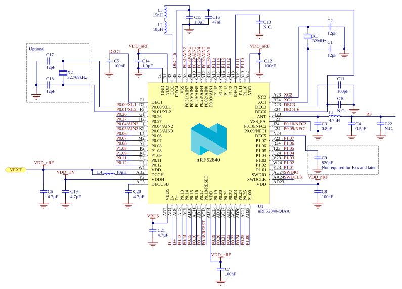
| Designator | Value v1.0 | Value v1.1 | Description | Footprint |
|---|---|---|---|---|
| C1, C2, C17, C18 | 12 pF | Capacitor, NP0, ±2% | 0402 | |
| C3 | 1 pF | 0.8 pF | Capacitor, NP0, ±10% | 0402 |
| C4 | 1 pF | 0.5 pF | Capacitor, NP0, ±10% | 0402 |
| C5, C7, C8, C12 | 100 nF | Capacitor, X7R, ±10% | 0402 | |
| C6, C20 | 4.7 µF | Capacitor, X7R, ±10% | 0603 | |
| C9 | 820 pF | Capacitor, NP0, ±5% Not required for Fxx and later | 0402 | |
| C10, C13, C22 | N.C. | Not mounted | 0402 | |
| C11 | 100 pF | Capacitor, NP0, ±5% | 0402 | |
| C14, C15 | 1.0 µF | Capacitor, X7R, ±10% | 0603 | |
| C16 | 47 nF | Capacitor, X7R, ±10% | 0402 | |
| C19, C21 | 4.7 µF | Capacitor, X7S, ±10% | 0603 | |
| L1 | 3.9 nH | 4.7 nH | High frequency chip inductor ±5% | 0402 |
| L2 | 10 µH | Chip inductor, IDC, min = 50 mA, ±20% | 0603 | |
| L3 | 15 nH | High frequency chip inductor ±10% | 0402 | |
| L4 | 10 µH | Chip inductor, IDC, min = 80 mA, ±20% | 0603 | |
| U1 | nRF52840-QIAA | Multiprotocol Bluetooth low energy, IEEE 802.15.4, ANT, and 2.4 GHz proprietary System on Chip | AQFN-73 | |
| X1 | 32 MHz | XTAL SMD 2016, 32 MHz, Cl=8 pF, Total Tol: ±40 ppm | XTAL_2016 | |
| X2 | 32.768 kHz | XTAL SMD 3215, 32.768 kHz, Cl=9 pF, Total Tol: ±50 ppm | XTAL_3215 | |
Circuit configuration no. 5 for QIAA aQFN73
Circuit configuration number 5 for QIAA aQFN73, showing the schematic and the bill of materials.
| Config no. | Supply configuration | Enabled features | |||||
|---|---|---|---|---|---|---|---|
| VDDH | VDD | EXTSUPPLY | DCDCEN0 | DCDCEN1 | USB | NFC | |
| Config. 5 | N/A | Battery/Ext. regulator | No | No | Yes | Yes | Yes |
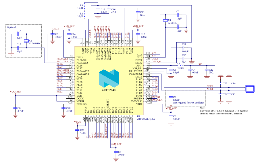
| Designator | Value v1.0 | Value v1.1 | Description | Footprint |
|---|---|---|---|---|
| C1, C2, C17, C18 | 12 pF | Capacitor, NP0, ±2% | 0402 | |
| C3 | 1 pF | 0.8 pF | Capacitor, NP0, ±10% | 0402 |
| C4 | 1 pF | 0.5 pF | Capacitor, NP0, ±10% | 0402 |
| C5, C7, C8, C12 | 100 nF | Capacitor, X7R, ±10% | 0402 | |
| C6, C20 | 4.7 µF | Capacitor, X7R, ±10% | 0603 | |
| C9 | 820 pF | Capacitor, NP0, ±5% | 0402 | |
| C10, C13, C22 | N.C. | Not mounted | 0402 | |
| C11 | 100 pF | Capacitor, NP0, ±5% | 0402 | |
| C14, C15 | 1.0 µF | Capacitor, X7R, ±10% | 0603 | |
| C16 | 47 nF | Capacitor, X7R, ±10% | 0402 | |
| C21 | 4.7 µF | Capacitor, X7S, ±10% | 0603 | |
| CT1, CT2, CT3, CT4 | Antenna dependent | Capacitor, NP0, ±5% | 0402 | |
| L1 | 3.9 nH | 4.7 nH | High frequency chip inductor ±5% | 0402 |
| L2 | 10 µH | Chip inductor, IDC, min = 50 mA, ±20% | 0603 | |
| L3 | 15 nH | High frequency chip inductor ±10% | 0402 | |
| U1 | nRF52840-QIAA | Multiprotocol Bluetooth low energy, IEEE 802.15.4, ANT, and 2.4 GHz proprietary System on Chip | AQFN-73 | |
| X1 | 32 MHz | XTAL SMD 2016, 32 MHz, Cl=8 pF, Total Tol: ±40 ppm | XTAL_2016 | |
| X2 | 32.768 kHz | XTAL 3215, 32.768 kHz, Cl=9 pF, Total Tol: ±50 ppm | XTAL_3215 | |
Circuit configuration no. 6 for QIAA aQFN73
Circuit configuration number 6 for QIAA aQFN73, showing the schematic and the bill of materials.
| Config no. | Supply configuration | Enabled features | |||||
|---|---|---|---|---|---|---|---|
| VDDH | VDD | EXTSUPPLY | DCDCEN0 | DCDCEN1 | USB | NFC | |
| Config. 6 | N/A | Battery/Ext. regulator | No | No | No | No | No |
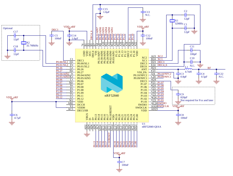
| Designator | Value v1.0 | Value v1.1 | Description | Footprint |
|---|---|---|---|---|
| C1, C2, C17, C18 | 12 pF | Capacitor, NP0, ±2% | 0402 | |
| C3 | 1 pF | 0.8 pF | Capacitor, NP0, ±10% | 0402 |
| C4 | 1 pF | 0.5 pF | Capacitor, NP0, ±10% | 0402 |
| C5, C7, C8, C12 | 100 nF | Capacitor, X7R, ±10% | 0402 | |
| C6 | 4.7 µF | Capacitor, X7R, ±10% | 0603 | |
| C9 | 820 pF | Capacitor, NP0, ±5% Not required for Fxx and later | 0402 | |
| C10, C13, C22 | N.C. | Not mounted | 0402 | |
| C11 | 100 pF | Capacitor, NP0, ±5% | 0402 | |
| C14, C15 | 1.0 µF | Capacitor, X7R, ±10% | 0603 | |
| L1 | 3.9 nH | 4.7 nH | High frequency chip inductor ±5% | 0402 |
| U1 | nRF52840-QIAA | Multiprotocol Bluetooth low energy, IEEE 802.15.4, ANT, and 2.4 GHz proprietary System on Chip | AQFN-73 | |
| X1 | 32 MHz | XTAL SMD 2016, 32 MHz, Cl=8 pF, Total Tol: ±40 ppm | XTAL_2016 | |
| X2 | 32.768 kHz | XTAL SMD 3215, 32.768 kHz, Cl=9 pF, Total Tol: ±50 ppm | XTAL_3215 | |
Circuit configuration no. 7 for QIAA aQFN73
Circuit configuration number 7 for QIAAaQFN73, showing the schematic and the bill of materials.
This circuit configuration includes a four-component RF match for improved harmonic suppression when using RADIO with TXPOWER ≥ 5 dBm.
| Config no. | Supply configuration | Enabled features | |||||
|---|---|---|---|---|---|---|---|
| VDDH | VDD | EXTSUPPLY | DCDCEN0 | DCDCEN1 | USB | NFC | |
| Config. 7 | Battery/Ext. regulator | N/A | Yes | Yes | Yes | Yes | No |
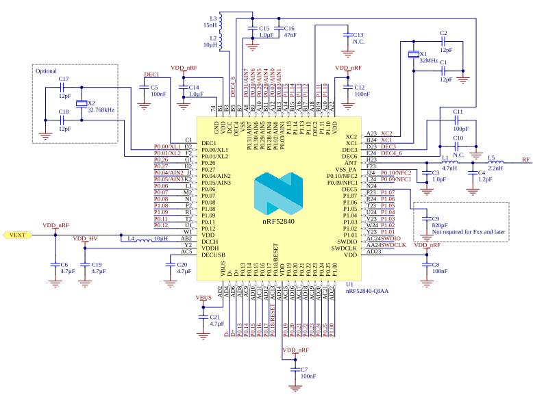
| Designator | Value | Description | Footprint |
|---|---|---|---|
| C1, C2, C17, C18 | 12 pF | Capacitor, NP0, ±2% | 0402 |
| C3 | 1 pF | Capacitor, NP0, ±5% | 0402 |
| C4 | 1.2 pF | Capacitor, NP0, ±5% | 0402 |
| C5, C7, C8, C12 | 100 nF | Capacitor, X7R, ±10% | 0402 |
| C6, C20 | 4.7 µF | Capacitor, X7R, ±10% | 0603 |
| C9 | 820 pF | Capacitor, NP0, ±5% Not required for Fxx and later | 0402 |
| C10, C13 | N.C. | Not mounted | 0402 |
| C11 | 100 pF | Capacitor, NP0, ±5% | 0402 |
| C14, C15 | 1.0 µF | Capacitor, X7R, ±10% | 0603 |
| C16 | 47 nF | Capacitor, X7R, ±10% | 0402 |
| C19, C21 | 4.7 µF | Capacitor, X7S, ±10% | 0603 |
| L1 | 4.7 nH | High frequency chip inductor ±5% | 0402 |
| L2 | 10 µH | Chip inductor, IDC, min = 50 mA, ±20% | 0603 |
| L3 | 15 nH | High frequency chip inductor ±10% | 0402 |
| L4 | 10 µH | Chip inductor, IDC, min = 80 mA, ±20% | 0603 |
| L5 | 2.2 nH | High frequency chip inductor ±5% | 0402 |
| U1 | nRF52840-QIAA | Multiprotocol Bluetooth low energy, IEEE 802.15.4, ANT, and 2.4 GHz proprietary System on Chip | AQFN-73 |
| X1 | 32 MHz | XTAL SMD 2016, 32 MHz, Cl=8 pF, Total Tol: ±40 ppm | XTAL_2016 |
| X2 | 32.768 kHz | XTAL SMD 3215, 32.768 kHz, Cl=9 pF, Total Tol: ±50 ppm | XTAL_3215 |
Circuit configuration no. 1 for QFAA QFN48
Circuit configuration number 1 for QFAA QFN48, showing the schematic and the bill of materials.
| Config no. | Supply configuration | Enabled features | |||||
|---|---|---|---|---|---|---|---|
| VDDH | VDD | EXTSUPPLY | DCDCEN0 | DCDCEN1 | USB | NFC | |
| Config. 1 | N/A | Battery/Ext. regulator | N/A | N/A | Yes | N/A | No |
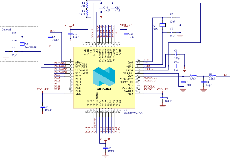
| Designator | Value | Description | Footprint |
|---|---|---|---|
| C1, C2, C16, C17 | 12 pF | Capacitor, NP0, ±2% | 0201 |
| C3 | 1.0 pF | Capacitor, NP0, ±10% | 0201 |
| C4 | 1.2 pF | Capacitor, NP0, ±10% | 0201 |
| C5, C6, C7, C8, C12 | 100 nF | Capacitor, X5R, ±10% | 0201 |
| C10 | N.C. | Not mounted | 0201 |
| C11 | 100 pF | Capacitor, NP0, ±5% | 0201 |
| C13, C14 | 1.0 µF | Capacitor, X5R, ±10% | 0402 |
| C15 | 47 nF | Capacitor, X5R, ±10% | 0201 |
| L1 | 4.7 nH | High frequency chip inductor ±5% | 0201 |
| L2 | 2.2 nH | High frequency chip inductor ±5% | 0201 |
| L3 | 10 µH | Chip inductor, IDC, min = 50 mA, ±20% | 0603 |
| L4 | 15 nH | High frequency chip inductor ±10% | 0402 |
| U1 | nRF52840-QFAA | Multiprotocol Bluetooth low energy, IEEE 802.15.4, ANT, and 2.4 GHz proprietary System on Chip | QFN48 |
| X1 | 32 MHz | XTAL SMD 2016, 32 MHz, Cl=8 pF, Total Tol: ±30 ppm | XTAL_2016 |
| X2 | 32.768 kHz | XTAL SMD 2012, 32.768 kHz, Cl=9 pF, Total Tol: ±50 ppm | XTAL_2012 |
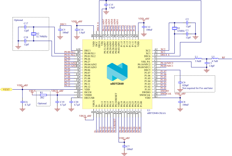
Circuit configuration no. 1 for CKAA WLCSP
Circuit configuration number 1 for CKAA WLCSP, showing the schematic and the bill of materials.
| Config no. | Supply configuration | Enabled features | |||||
|---|---|---|---|---|---|---|---|
| VDDH | VDD | EXTSUPPLY | DCDCEN0 | DCDCEN1 | USB | NFC | |
| Config. 1 | USB (VDDH = VBUS) | N/A | Yes | No | No | Yes | No |
| Designator | Value | Description | Footprint |
|---|---|---|---|
| C1, C2, C17, C18 | 12 pF | Capacitor, NP0, ±2% | 0201 |
| C3 | 1.0 pF | Capacitor, NP0, ±5% | 0201 |
| C5, C7, C8, C12 | 100 nF | Capacitor, X7R, ±10% | 0201 |
| C6, C20 | 4.7 µF | Capacitor, X7R, ±10% | 0603 |
| C9 | 820 pF | Capacitor, X7R, ±10% Not required for Fxx and later | 0201 |
| C14, C15 | 1.0 µF | Capacitor, X7R, ±10% | 0603 |
| C19 | 4.7 µF | Capacitor, X7S, ±10% | 0603 |
| L1 | 3.9 nH | High frequency chip inductor ±5% | 0201 |
| L5 | 4.7 nH | High frequency chip inductor ±5% | 0201 |
| R1 | 2R2 | Resistor, ±1%, 0.05W | 0201 |
| U1 | nRF52840-CKAA | Multiprotocol Bluetooth low energy, IEEE 802.15.4, ANT, and 2.4 GHz proprietary System on Chip | WLCSP-94 |
| X1 | 32 MHz | XTAL SMD 2016, 32 MHz, Cl=8 pF, Total Tol: ±40 ppm | XTAL_2016 |
| X2 | 32.768 kHz | XTAL SMD 2012, 32.768 kHz, Cl=9 pF, Total Tol: ±50 ppm | XTAL_2012 |
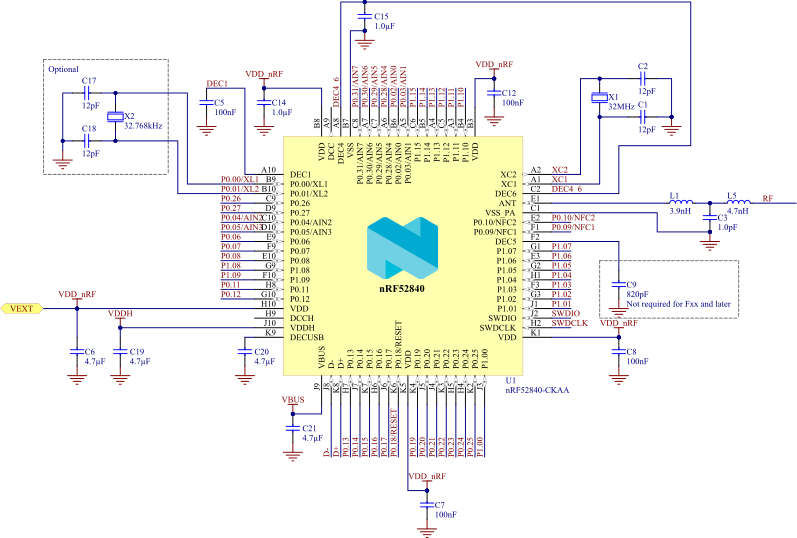
Circuit configuration no. 2 for CKAA WLCSP
Circuit configuration number 2 for CKAA WLCSP, showing the schematic and the bill of materials.
| Config no. | Supply configuration | Enabled features | |||||
|---|---|---|---|---|---|---|---|
| VDDH | VDD | EXTSUPPLY | DCDCEN0 | DCDCEN1 | USB | NFC | |
| Config. 2 | Battery/Ext. regulator | N/A | Yes | No | No | Yes | No |
| Designator | Value | Description | Footprint |
|---|---|---|---|
| C1, C2, C17, C18 | 12 pF | Capacitor, NP0, ±2% | 0201 |
| C3 | 1.0 pF | Capacitor, NP0, ±5% | 0201 |
| C5, C7, C8, C12 | 100 nF | Capacitor, X7R, ±10% | 0201 |
| C6, C20 | 4.7 µF | Capacitor, X7R, ±10% | 0603 |
| C9 | 820 pF | Capacitor, X7R, ±10% Not required for Fxx and later | 0201 |
| C14, C15 | 1.0 µF | Capacitor, X7R, ±10% | 0603 |
| C19, C21 | 4.7 µF | Capacitor, X7S, ±10% | 0603 |
| L1 | 3.9 nH | High frequency chip inductor ±5% | 0201 |
| L5 | 4.7 nH | High frequency chip inductor ±5% | 0201 |
| U1 | nRF52840-CKAA | Multiprotocol Bluetooth low energy, IEEE 802.15.4, ANT, and 2.4 GHz proprietary System on Chip | WLCSP-94 |
| X1 | 32 MHz | XTAL SMD 2016, 32 MHz, Cl=8 pF, Total Tol: ±40 ppm | XTAL_2016 |
| X2 | 32.768 kHz | XTAL SMD 2012, 32.768 kHz, Cl=9 pF, Total Tol: ±50 ppm | XTAL_2012 |
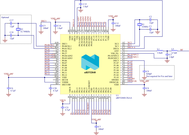
Circuit configuration no. 3 for CKAA WLCSP
Circuit configuration number 3 for CKAA WLCSP, showing the schematic and the bill of materials.
| Config no. | Supply configuration | Enabled features | |||||
|---|---|---|---|---|---|---|---|
| VDDH | VDD | EXTSUPPLY | DCDCEN0 | DCDCEN1 | USB | NFC | |
| Config. 3 | N/A | Battery/Ext. regulator | No | No | No | Yes | No |
| Designator | Value | Description | Footprint |
|---|---|---|---|
| C1, C2, C17, C18 | 12 pF | Capacitor, NP0, ±2% | 0201 |
| C3 | 1.0 pF | Capacitor, NP0, ±5% | 0201 |
| C5, C7, C8, C12 | 100 nF | Capacitor, X7R, ±10% | 0201 |
| C6, C20 | 4.7 µF | Capacitor, X7R, ±10% | 0603 |
| C9 | 820 pF | Capacitor, X7R, ±10% Not required for Fxx and later | 0201 |
| C14, C15 | 1.0 µF | Capacitor, X7R, ±10% | 0603 |
| C21 | 4.7 µF | Capacitor, X7S, ±10% | 0603 |
| L1 | 3.9 nH | High frequency chip inductor ±5% | 0201 |
| L5 | 4.7 nH | High frequency chip inductor ±5% | 0201 |
| U1 | nRF52840-CKAA | Multiprotocol Bluetooth low energy, IEEE 802.15.4, ANT, and 2.4 GHz proprietary System on Chip | WLCSP-94 |
| X1 | 32 MHz | XTAL SMD 2016, 32 MHz, Cl=8 pF, Total Tol: ±40 ppm | XTAL_2016 |
| X2 | 32.768 kHz | XTAL SMD 2012, 32.768 kHz, Cl=9 pF, Total Tol: ±50 ppm | XTAL_2012 |
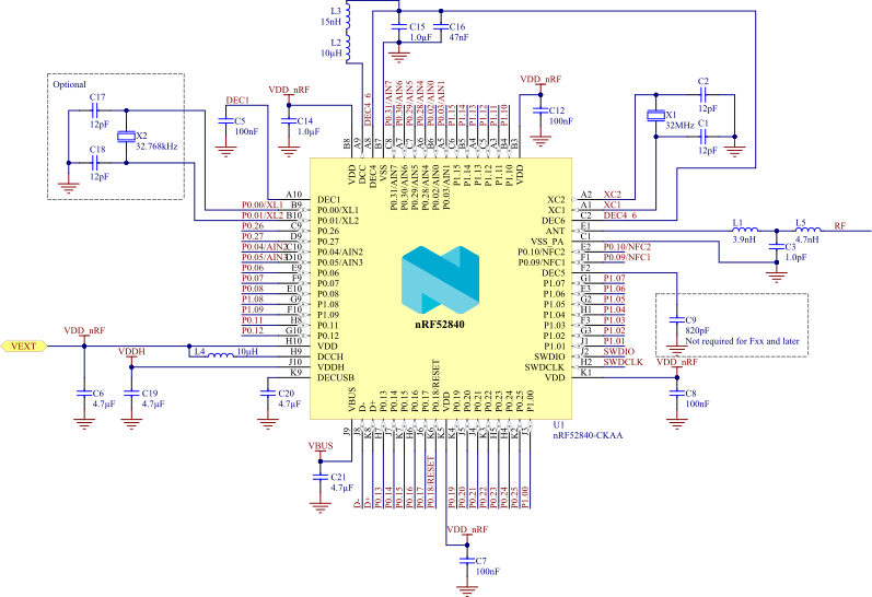
Circuit configuration no. 4 for CKAA WLCSP
Circuit configuration number 4 for CKAA WLCSP, showing the schematic and the bill of materials.
| Config no. | Supply configuration | Enabled features | |||||
|---|---|---|---|---|---|---|---|
| VDDH | VDD | EXTSUPPLY | DCDCEN0 | DCDCEN1 | USB | NFC | |
| Config. 4 | Battery/Ext. regulator | N/A | Yes | Yes | Yes | Yes | No |
| Designator | Value | Description | Footprint |
|---|---|---|---|
| C1, C2, C17, C18 | 12 pF | Capacitor, NP0, ±2% | 0201 |
| C3 | 1.0 pF | Capacitor, NP0, ±5% | 0201 |
| C5, C7, C8, C12 | 100 nF | Capacitor, X7R, ±10% | 0201 |
| C6, C20 | 4.7 µF | Capacitor, X7R, ±10% | 0603 |
| C9 | 820 pF | Capacitor, X7R, ±10% Not required for Fxx and later | 0201 |
| C14, C15 | 1.0 µF | Capacitor, X7R, ±10% | 0603 |
| C16 | 47 nF | Capacitor, X7R, ±10% | 0201 |
| C19, C21 | 4.7 µF | Capacitor, X7S, ±10% | 0603 |
| L1 | 3.9 nH | High frequency chip inductor ±5% | 0201 |
| L2 | 10 µH | Chip inductor, IDC, min = 50 mA, ±20% | 0603 |
| L3 | 15 nH | High frequency chip inductor ±10% | 0402 |
| L4 | 10 µH | Chip inductor, IDC, min = 80 mA, ±10% | 0603 |
| L5 | 4.7 nH | High frequency chip inductor ±5% | 0201 |
| U1 | nRF52840-CKAA | Multiprotocol Bluetooth low energy, IEEE 802.15.4, ANT, and 2.4 GHz proprietary System on Chip | WLCSP-94 |
| X1 | 32 MHz | XTAL SMD 2016, 32 MHz, Cl=8 pF, Total Tol: ±40 ppm | XTAL_2016 |
| X2 | 32.768 kHz | XTAL SMD 2012, 32.768 kHz, Cl=9 pF, Total Tol: ±50 ppm | XTAL_2012 |
Circuit configuration no. 5 for CKAA WLCSP
Circuit configuration number 5 for CKAA WLCSP, showing the schematic and the bill of materials.
| Config no. | Supply configuration | Enabled features | |||||
|---|---|---|---|---|---|---|---|
| VDDH | VDD | EXTSUPPLY | DCDCEN0 | DCDCEN1 | USB | NFC | |
| Config. 5 | N/A | Battery/Ext. regulator | No | No | Yes | Yes | Yes |
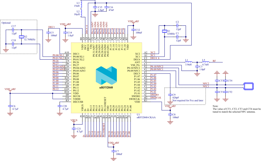
| Designator | Value | Description | Footprint |
|---|---|---|---|
| C1, C2, C17, C18 | 12 pF | Capacitor, NP0, ±2% | 0201 |
| C3 | 1.0 pF | Capacitor, NP0, ±5% | 0201 |
| C5, C7, C8, C12 | 100 nF | Capacitor, X7R, ±10% | 0201 |
| C6, C20 | 4.7 µF | Capacitor, X7R, ±10% | 0603 |
| C9 | 820 pF | Capacitor, X7R, ±10% Not required for Fxx and later | 0201 |
| C14, C15 | 1.0 µF | Capacitor, X7R, ±10% | 0603 |
| C16 | 47 nF | Capacitor, X7R, ± 10% | 0201 |
| C21 | 4.7 µF | Capacitor, X7S, ± 10% | 0603 |
| CT1, CT2, CT3, CT4 | Antenna dependent | Capacitor, X7R, ± 10% | 0201 |
| L1 | 3.9 nH | High frequency chip inductor ±5% | 0201 |
| L2 | 10 µH | Chip inductor, IDC, min = 50 mA, ±20% | 0603 |
| L3 | 15 nH | High frequency chip inductor ±10% | 0402 |
| L5 | 4.7 nH | High frequency chip inductor ±5% | 0201 |
| U1 | nRF52840-CKAA | Multiprotocol Bluetooth low energy, IEEE 802.15.4, ANT, and 2.4 GHz proprietary System on Chip | WLCSP-94 |
| X1 | 32 MHz | XTAL SMD 2016, 32 MHz, Cl=8 pF, Total Tol: ±40 ppm | XTAL_2016 |
| X2 | 32.768 kHz | XTAL SMD 2012, 32.768 kHz, Cl=9 pF, Total Tol: ±50 ppm | XTAL_2012 |
Circuit configuration no. 6 for CKAA WLCSP
Circuit configuration number 6 for CKAA WLCSP, showing the schematic and the bill of materials.
| Config no. | Supply configuration | Enabled features | |||||
|---|---|---|---|---|---|---|---|
| VDDH | VDD | EXTSUPPLY | DCDCEN0 | DCDCEN1 | USB | NFC | |
| Config. 6 | N/A | Battery/Ext. regulator | No | No | No | No | No |
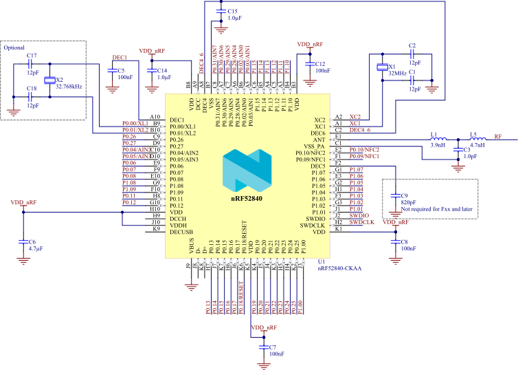
| Designator | Value | Description | Footprint |
|---|---|---|---|
| C1, C2, C17, C18 | 12 pF | Capacitor, NP0, ±2% | 0201 |
| C3 | 1.0 pF | Capacitor, NP0, ±5% | 0201 |
| C5, C7, C8, C12 | 100 nF | Capacitor, X7R, ±10% | 0201 |
| C6 | 4.7 µF | Capacitor, X7R, ±10% | 0603 |
| C9 | 820 pF | Capacitor, X7R, ±10% Not required for Fxx and later | 0201 |
| C14, C15 | 1.0 µF | Capacitor, X7R, ±10% | 0603 |
| L1 | 3.9 nH | High frequency chip inductor ±5% | 0201 |
| L5 | 4.7 nH | High frequency chip inductor ±5% | 0201 |
| U1 | nRF52840-CKAA | Multiprotocol Bluetooth low energy, IEEE 802.15.4, ANT, and 2.4 GHz proprietary System on Chip | WLCSP-94 |
| X1 | 32 MHz | XTAL SMD 2016, 32 MHz, Cl=8 pF, Total Tol: ±40 ppm | XTAL_2016 |
| X2 | 32.768 kHz | XTAL SMD 2012, 32.768 kHz, Cl=9 pF, Total Tol: ±50 ppm | XTAL_2012 |
PCB guidelines
A well designed PCB is necessary to achieve good RF performance. Poor layout can lead to loss in performance or functionality.
A qualified RF layout for the IC and its surrounding components, including matching networks, can be downloaded from www.nordicsemi.com.
To ensure optimal performance it is essential that you follow the schematics and layout references closely. Especially in the case of the antenna matching circuitry (components between device pin ANT and the antenna), any changes to the layout can change the behavior, resulting in degradation of RF performance or a need to change component values. All reference circuits are designed for use with a 50 Ω single-ended antenna.
A PCB with a minimum of two layers, including a ground plane, is recommended for optimal RF performance. On PCBs with more than two layers, put a keep-out area on the inner layers directly below the antenna matching circuitry (components between device pin ANT and the antenna) to reduce the stray capacitances that influence RF performance.
A matching network is needed between the RF pin ANT and the antenna, to match the antenna impedance (normally 50 Ω) to the optimum RF load impedance for the chip. For optimum performance, the impedance for the matching network should be set as described in the recommended aQFN™73 package reference circuitry from Circuit configuration no. 1 for QIAA aQFN73, the recommended QFN48 reference circuitry from Circuit configuration no. 1 for QFAA QFN48, or the recommended WLCSP reference circuitry from Circuit configuration no. 1 for CKAA WLCSP depending on the package variant used in your design.
The DC supply voltage should be decoupled as close as possible to the VDD pins with high performance RF capacitors. See the schematics for recommended decoupling capacitor values. The supply voltage for the chip should be filtered and routed separately from the supply voltages of any digital circuitry.
Long power supply lines on the PCB should be avoided. All device grounds, VDD connections, and VDD bypass capacitors must be connected as close as possible to the IC. For a PCB with a topside RF ground plane, the VSS pins should be connected directly to the ground plane. For a PCB with a bottom ground plane, the best technique is to have via holes as close as possible to the VSS pads. A minimum of one via hole should be used for each VSS pin.
Fast switching digital signals should not be routed close to the crystal or the power supply lines. Capacitive loading of fast switching digital output lines should be minimized in order to avoid radio interference. Avoid routing the 32MHz crystal lines close to antenna line and antenna ground.
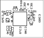
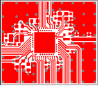
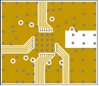
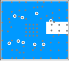
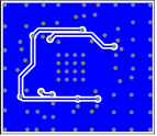
PCB layout example
The PCB layout shown in the following figures is a reference layout for the aQFN™ package with internal LDO setup and VBUS supply.
For all available reference layouts, see the product page for the nRF52840 on www.nordicsemi.com.
PMIC support
The nRF52 Series is comprehensively supported by Nordic Semiconductor's own range of PMICs (Power Management Integrated Circuits). These PMICs are meticulously designed to enhance the performance and efficiency of the nRF52 Series devices. This integration ensures the longest battery life and the highest reliability for the end application. The synergy between the nRF52 Series and the Nordic PMICs highlights Nordic Semiconductor's commitment to providing a complete and cohesive solution for their customers' needs in wireless technology applications.