REGULATORS — Regulator control
All system components are powered from the on-chip voltage regulators. These regulators are responsible for converting the voltage supplied on the VDD or VDDH pins to adequate voltages to be used internally.
The available regulators can be configured in multiple ways to accommodate different input voltage ranges. Some modes support sourcing power to external circuitry. The voltage modes that are supported by nRF5340 are listed in the following table.
| Voltage mode | Input voltage range | Output voltage range |
|---|---|---|
| Normal voltage mode | 1.7 V to 3.6 V | - |
| High voltage mode | 2.5 V to 5.5 V | 1.8 V to 3.3 V |
For an overview on the available regulators, see Power supply modes and regulators.
Normal voltage mode
Normal voltage mode uses the main regulator (VREGMAIN) and the radio regulator (VREGRADIO).
The VREGMAIN and VREGRADIO regulators operate in LDO mode by default. DC/DC mode is enabled independently for each regulator using VREGMAIN.DCDCEN (Retained) and VREGRADIO.DCDCEN (Retained) respectively.
When configured as shown in the following figure, nRF5340 enters normal voltage mode. Here both regulators are in DC/DC mode. An external LC filter is required for each regulator in DC/DC mode. If a regulator is only to be used in LDO mode, the inductor for this regulator is not needed. In this mode, the VDDH pin must be connected to VDD, even if the high voltage regulator (VREGH) is not in use.
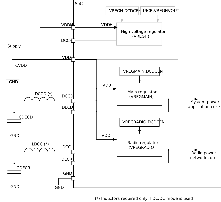
Operating a regulator in DC/DC mode reduces the overall power consumption due to higher efficiency than in LDO mode. Regulator efficiency in DC/DC mode varies depending on the supply voltage and the current drawn from the regulators.
High voltage mode
High voltage mode uses the main regulator (VREGMAIN), the high voltage regulator (VREGH), and the radio regulator (VREGRADIO).
All regulators operate in LDO mode by default. DC/DC mode is enabled independently for each regulator using VREGMAIN.DCDCEN (Retained), VREGH.DCDCEN (Retained), and VREGRADIO.DCDCEN (Retained).
When configured as shown in the following figure, nRF5340 enters high voltage mode. Here all three regulators are in DC/DC mode. An external LC filter is required for each of the regulators in DC/DC mode. The inductor is not needed when the regulator is exclusively in LDO mode.
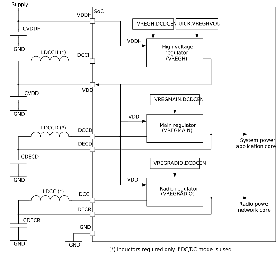
Operating a regulator in DC/DC mode reduces the overall power consumption due to higher efficiency than in LDO mode. Regulator efficiency in DC/DC mode varies depending on the supply voltage and the current drawn from the regulators.
External circuitry supply
In high voltage mode, the output from VREGH can be used to supply external circuitry from the VDD pin.
As illustrated in High voltage mode, external circuitry can be powered from the VDD pin. The VDD output voltage is programmed in the register UICR.VREGHVOUT.
The supported output voltage range depends on the supply voltage provided to the VDDH pin. The difference between voltage supplied on the VDDH pin and the voltage output on the VDD pin is defined by the VREGH,DROP parameter in Regulator specifications, VREGH stage.
Supplying power to external circuitry is allowed in both System OFF and System ON mode.
GPIO levels
The GPIO high reference voltage depends on the regulator voltage mode.
In normal voltage mode, the GPIO high level equals the voltage supplied to the VDD pin. In high voltage mode, it equals the level specified in the VREGHVOUT register.
Registers
Instances
| Instance | Domain | Base address | TrustZone | Split access | Description | ||
|---|---|---|---|---|---|---|---|
| Map | Att | DMA | |||||
REGULATORS : S | APPLICATION | 0x50004000 | US | S | NA | No | Regulator configuration |
Register overview
| Register | Offset | TZ | Description |
|---|---|---|---|
| MAINREGSTATUS | 0x428 | Main supply status This register is retained. | |
| SYSTEMOFF | 0x500 | System OFF register | |
| POFCON | 0x510 | Power-fail comparator configuration This register is retained. | |
| VREGMAIN.DCDCEN | 0x704 | DC/DC enable register for VREGMAIN This register is retained. | |
| VREGRADIO.DCDCEN | 0x904 | DC/DC enable register for VREGRADIO This register is retained. | |
| VREGH.DCDCEN | 0xB00 | DC/DC enable register for VREGH This register is retained. | |
| VREGH.EXTSILENTEN | 0xB40 | When VREGH is in DC/DC mode, enable VREGH silent mode to supply external components from VDD. Silent mode has lower voltage ripple. Silent mode is used when DC/DC is enabled, and is ignored in LDO mode. Disabling silent mode reduces current consumption in sleep. This register is retained. |
MAINREGSTATUS (Retained)
Address offset: 0x428
Main supply status
This register is retained.
| Bit number | 31 | 30 | 29 | 28 | 27 | 26 | 25 | 24 | 23 | 22 | 21 | 20 | 19 | 18 | 17 | 16 | 15 | 14 | 13 | 12 | 11 | 10 | 9 | 8 | 7 | 6 | 5 | 4 | 3 | 2 | 1 | 0 | |||
|---|---|---|---|---|---|---|---|---|---|---|---|---|---|---|---|---|---|---|---|---|---|---|---|---|---|---|---|---|---|---|---|---|---|---|---|
| ID | A | ||||||||||||||||||||||||||||||||||
| Reset 0x00000000 | 0 | 0 | 0 | 0 | 0 | 0 | 0 | 0 | 0 | 0 | 0 | 0 | 0 | 0 | 0 | 0 | 0 | 0 | 0 | 0 | 0 | 0 | 0 | 0 | 0 | 0 | 0 | 0 | 0 | 0 | 0 | 0 | |||
| ID | R/W | Field | Value ID | Value | Description | ||||||||||||||||||||||||||||||
| A | R | VREGH | VREGH status | ||||||||||||||||||||||||||||||||
Inactive | 0 | Normal voltage mode. Voltage supplied on VDD and VDDH. | |||||||||||||||||||||||||||||||||
Active | 1 | High voltage mode. Voltage supplied on VDDH. | |||||||||||||||||||||||||||||||||
SYSTEMOFF
Address offset: 0x500
System OFF register
| Bit number | 31 | 30 | 29 | 28 | 27 | 26 | 25 | 24 | 23 | 22 | 21 | 20 | 19 | 18 | 17 | 16 | 15 | 14 | 13 | 12 | 11 | 10 | 9 | 8 | 7 | 6 | 5 | 4 | 3 | 2 | 1 | 0 | |||
|---|---|---|---|---|---|---|---|---|---|---|---|---|---|---|---|---|---|---|---|---|---|---|---|---|---|---|---|---|---|---|---|---|---|---|---|
| ID | A | ||||||||||||||||||||||||||||||||||
| Reset 0x00000000 | 0 | 0 | 0 | 0 | 0 | 0 | 0 | 0 | 0 | 0 | 0 | 0 | 0 | 0 | 0 | 0 | 0 | 0 | 0 | 0 | 0 | 0 | 0 | 0 | 0 | 0 | 0 | 0 | 0 | 0 | 0 | 0 | |||
| ID | R/W | Field | Value ID | Value | Description | ||||||||||||||||||||||||||||||
| A | W | SYSTEMOFF | Enable System OFF mode | ||||||||||||||||||||||||||||||||
Enter | 1 | Enable System OFF mode | |||||||||||||||||||||||||||||||||
POFCON (Retained)
Address offset: 0x510
Power-fail comparator configuration
This register is retained.
| Bit number | 31 | 30 | 29 | 28 | 27 | 26 | 25 | 24 | 23 | 22 | 21 | 20 | 19 | 18 | 17 | 16 | 15 | 14 | 13 | 12 | 11 | 10 | 9 | 8 | 7 | 6 | 5 | 4 | 3 | 2 | 1 | 0 | |||
|---|---|---|---|---|---|---|---|---|---|---|---|---|---|---|---|---|---|---|---|---|---|---|---|---|---|---|---|---|---|---|---|---|---|---|---|
| ID | C | C | C | C | B | B | B | B | A | ||||||||||||||||||||||||||
| Reset 0x00000000 | 0 | 0 | 0 | 0 | 0 | 0 | 0 | 0 | 0 | 0 | 0 | 0 | 0 | 0 | 0 | 0 | 0 | 0 | 0 | 0 | 0 | 0 | 0 | 0 | 0 | 0 | 0 | 0 | 0 | 0 | 0 | 0 | |||
| ID | R/W | Field | Value ID | Value | Description | ||||||||||||||||||||||||||||||
| A | RW | POF | Enable or disable power-fail comparator | ||||||||||||||||||||||||||||||||
Disabled | 0 | Disable | |||||||||||||||||||||||||||||||||
Enabled | 1 | Enable | |||||||||||||||||||||||||||||||||
| B | RW | THRESHOLD | Power-fail comparator threshold setting | ||||||||||||||||||||||||||||||||
V19 | 6 | Set threshold to 1.9 V | |||||||||||||||||||||||||||||||||
V20 | 7 | Set threshold to 2.0 V | |||||||||||||||||||||||||||||||||
V21 | 8 | Set threshold to 2.1 V | |||||||||||||||||||||||||||||||||
V22 | 9 | Set threshold to 2.2 V | |||||||||||||||||||||||||||||||||
V23 | 10 | Set threshold to 2.3 V | |||||||||||||||||||||||||||||||||
V24 | 11 | Set threshold to 2.4 V | |||||||||||||||||||||||||||||||||
V25 | 12 | Set threshold to 2.5 V | |||||||||||||||||||||||||||||||||
V26 | 13 | Set threshold to 2.6 V | |||||||||||||||||||||||||||||||||
V27 | 14 | Set threshold to 2.7 V | |||||||||||||||||||||||||||||||||
V28 | 15 | Set threshold to 2.8 V | |||||||||||||||||||||||||||||||||
| C | RW | THRESHOLDVDDH | Power-fail comparator threshold setting for voltage supply on VDDH | ||||||||||||||||||||||||||||||||
V27 | 0 | Set threshold to 2.7 V | |||||||||||||||||||||||||||||||||
V28 | 1 | Set threshold to 2.8 V | |||||||||||||||||||||||||||||||||
V29 | 2 | Set threshold to 2.9 V | |||||||||||||||||||||||||||||||||
V30 | 3 | Set threshold to 3.0 V | |||||||||||||||||||||||||||||||||
V31 | 4 | Set threshold to 3.1 V | |||||||||||||||||||||||||||||||||
V32 | 5 | Set threshold to 3.2 V | |||||||||||||||||||||||||||||||||
V33 | 6 | Set threshold to 3.3 V | |||||||||||||||||||||||||||||||||
V34 | 7 | Set threshold to 3.4 V | |||||||||||||||||||||||||||||||||
V35 | 8 | Set threshold to 3.5 V | |||||||||||||||||||||||||||||||||
V36 | 9 | Set threshold to 3.6 V | |||||||||||||||||||||||||||||||||
V37 | 10 | Set threshold to 3.7 V | |||||||||||||||||||||||||||||||||
V38 | 11 | Set threshold to 3.8 V | |||||||||||||||||||||||||||||||||
V39 | 12 | Set threshold to 3.9 V | |||||||||||||||||||||||||||||||||
V40 | 13 | Set threshold to 4.0 V | |||||||||||||||||||||||||||||||||
V41 | 14 | Set threshold to 4.1 V | |||||||||||||||||||||||||||||||||
V42 | 15 | Set threshold to 4.2 V | |||||||||||||||||||||||||||||||||
VREGMAIN.DCDCEN (Retained)
Address offset: 0x704
DC/DC enable register for VREGMAIN
This register is retained.
| Bit number | 31 | 30 | 29 | 28 | 27 | 26 | 25 | 24 | 23 | 22 | 21 | 20 | 19 | 18 | 17 | 16 | 15 | 14 | 13 | 12 | 11 | 10 | 9 | 8 | 7 | 6 | 5 | 4 | 3 | 2 | 1 | 0 | |||
|---|---|---|---|---|---|---|---|---|---|---|---|---|---|---|---|---|---|---|---|---|---|---|---|---|---|---|---|---|---|---|---|---|---|---|---|
| ID | A | ||||||||||||||||||||||||||||||||||
| Reset 0x00000000 | 0 | 0 | 0 | 0 | 0 | 0 | 0 | 0 | 0 | 0 | 0 | 0 | 0 | 0 | 0 | 0 | 0 | 0 | 0 | 0 | 0 | 0 | 0 | 0 | 0 | 0 | 0 | 0 | 0 | 0 | 0 | 0 | |||
| ID | R/W | Field | Value ID | Value | Description | ||||||||||||||||||||||||||||||
| A | RW | DCDCEN | Enable or disable DC/DC converter | ||||||||||||||||||||||||||||||||
Disabled | 0 | Disable | |||||||||||||||||||||||||||||||||
Enabled | 1 | Enable | |||||||||||||||||||||||||||||||||
VREGRADIO.DCDCEN (Retained)
Address offset: 0x904
DC/DC enable register for VREGRADIO
This register is retained.
| Bit number | 31 | 30 | 29 | 28 | 27 | 26 | 25 | 24 | 23 | 22 | 21 | 20 | 19 | 18 | 17 | 16 | 15 | 14 | 13 | 12 | 11 | 10 | 9 | 8 | 7 | 6 | 5 | 4 | 3 | 2 | 1 | 0 | |||
|---|---|---|---|---|---|---|---|---|---|---|---|---|---|---|---|---|---|---|---|---|---|---|---|---|---|---|---|---|---|---|---|---|---|---|---|
| ID | A | ||||||||||||||||||||||||||||||||||
| Reset 0x00000000 | 0 | 0 | 0 | 0 | 0 | 0 | 0 | 0 | 0 | 0 | 0 | 0 | 0 | 0 | 0 | 0 | 0 | 0 | 0 | 0 | 0 | 0 | 0 | 0 | 0 | 0 | 0 | 0 | 0 | 0 | 0 | 0 | |||
| ID | R/W | Field | Value ID | Value | Description | ||||||||||||||||||||||||||||||
| A | RW | DCDCEN | Enable or disable DC/DC converter | ||||||||||||||||||||||||||||||||
Disabled | 0 | Disable | |||||||||||||||||||||||||||||||||
Enabled | 1 | Enable | |||||||||||||||||||||||||||||||||
VREGH.DCDCEN (Retained)
Address offset: 0xB00
DC/DC enable register for VREGH
This register is retained.
| Bit number | 31 | 30 | 29 | 28 | 27 | 26 | 25 | 24 | 23 | 22 | 21 | 20 | 19 | 18 | 17 | 16 | 15 | 14 | 13 | 12 | 11 | 10 | 9 | 8 | 7 | 6 | 5 | 4 | 3 | 2 | 1 | 0 | |||
|---|---|---|---|---|---|---|---|---|---|---|---|---|---|---|---|---|---|---|---|---|---|---|---|---|---|---|---|---|---|---|---|---|---|---|---|
| ID | A | ||||||||||||||||||||||||||||||||||
| Reset 0x00000000 | 0 | 0 | 0 | 0 | 0 | 0 | 0 | 0 | 0 | 0 | 0 | 0 | 0 | 0 | 0 | 0 | 0 | 0 | 0 | 0 | 0 | 0 | 0 | 0 | 0 | 0 | 0 | 0 | 0 | 0 | 0 | 0 | |||
| ID | R/W | Field | Value ID | Value | Description | ||||||||||||||||||||||||||||||
| A | RW | DCDCEN | Enable or disable DC/DC converter | ||||||||||||||||||||||||||||||||
Disabled | 0 | Disable | |||||||||||||||||||||||||||||||||
Enabled | 1 | Enable | |||||||||||||||||||||||||||||||||
VREGH.EXTSILENTEN (Retained)
Address offset: 0xB40
When VREGH is in DC/DC mode, enable VREGH silent mode to supply external components from VDD. Silent mode has lower voltage ripple.
Silent mode is used when DC/DC is enabled, and is ignored in LDO mode. Disabling silent mode reduces current consumption in sleep.
This register is retained.
| Bit number | 31 | 30 | 29 | 28 | 27 | 26 | 25 | 24 | 23 | 22 | 21 | 20 | 19 | 18 | 17 | 16 | 15 | 14 | 13 | 12 | 11 | 10 | 9 | 8 | 7 | 6 | 5 | 4 | 3 | 2 | 1 | 0 | |||
|---|---|---|---|---|---|---|---|---|---|---|---|---|---|---|---|---|---|---|---|---|---|---|---|---|---|---|---|---|---|---|---|---|---|---|---|
| ID | A | ||||||||||||||||||||||||||||||||||
| Reset 0x00000001 | 0 | 0 | 0 | 0 | 0 | 0 | 0 | 0 | 0 | 0 | 0 | 0 | 0 | 0 | 0 | 0 | 0 | 0 | 0 | 0 | 0 | 0 | 0 | 0 | 0 | 0 | 0 | 0 | 0 | 0 | 0 | 1 | |||
| ID | R/W | Field | Value ID | Value | Description | ||||||||||||||||||||||||||||||
| A | RW | EXTSILENTEN | Enable silent external DC/DC supply | ||||||||||||||||||||||||||||||||
Disabled | 0 | Disable | |||||||||||||||||||||||||||||||||
Enabled | 1 | Enable | |||||||||||||||||||||||||||||||||
Electrical specification
Recommended operating conditions
| Symbol | Description | Min. | Typ. | Max. | Units |
|---|---|---|---|---|---|
| VDD,POR | VDD supply voltage needed during power-on reset. | 1.75 | V | ||
| VDD | Normal voltage mode operating voltage. | 1.7 | 3.6 | V | |
| VDDH | High voltage mode operating voltage. | 2.5 | 5.5 | V |
Regulator specifications, VREGH stage
| Symbol | Description | Min. | Typ. | Max. | Units |
|---|---|---|---|---|---|
| VDDOUT | VDD output voltage. | 1.8 | 3.3 | V | |
| VDDOUT,ERR | VDD output voltage error (deviation from setting in ). | -10 | +5 | % | |
| IEXT,OFF | External current draw1 allowed in high voltage mode (supply on VDDH) during System OFF. | 1 | mA | ||
| IEXT,DCDC | External current draw1 allowed in High Voltage mode (supply on VDDH) when VREGMAIN and VREGRADIO are in DC/DC mode. Assumes worst-case power consumption from both cores2, and at the lowest VDD output voltage setting. | 7 | mA | ||
| IEXT,LDO | External current draw1 allowed in High Voltage mode (supply on VDDH) when VREGMAIN and VREGRADIO are in LDO mode. Assumes worst-case power consumption from both cores2, and at the lowest VDD output voltage setting. | 1 | mA | ||
| VREGH,DROP | Required difference between input voltage (VDDH) and output voltage (VDD, configured in VREGHVOUT), VDDH > VDD | 0.3 | V |
Regulator startup times
| Symbol | Description | Min. | Typ. | Max. | Units |
|---|---|---|---|---|---|
| tRISE,VREGHOUT | VREGH output (VDD) rise time after VDDH reaches minimum VDDH supply voltage | .. | .. | .. | |
| tRISE,VREGHOUT,10us | VDDH rise time 10 µs | 0.2 | 1.6 | ms | |
| tRISE,VREGHOUT,10ms | VDDH rise time 10 ms | 5 | ms | ||
| tRISE,VREGHOUT,50ms | VDDH rise time 50 ms | 30 | 50 | 80 | ms |
Power-fail comparator
| Symbol | Description | Min. | Typ. | Max. | Units |
|---|---|---|---|---|---|
| VPOF,NV | Nominal power level warning thresholds (falling supply voltage) in normal voltage mode (supply on VDD). Levels are configurable between min. and max. in increments of 100 mV. | 1.7 | 2.8 | V | |
| VPOF,HV | Nominal power level warning thresholds (falling supply voltage) in high Voltage mode (supply on VDDH). Levels are configurable between min. and max. in increments of 100 mV. | 2.7 | 4.2 | V | |
| VPOFTOL | Threshold voltage tolerance (applies in both normal voltage mode and high voltage mode). | -5 | +5 | % | |
| VPOFHYST | Threshold voltage hysteresis (applies in both normal voltage mode and high voltage mode). | 40 | 50 | 60 | mV |
| VBOR,OFF | Brownout reset voltage range System OFF mode. Brownout only applies to the voltage on VDD. | 1.54 | 1.64 | V | |
| VBOR,ON | Brownout reset voltage range System ON mode. Brownout only applies to the voltage on VDD. | 1.57 | 1.63 | V |