OSCILLATORS — Oscillator control
The system oscillators are shared between the cores in the system and automatically controlled by the clock control system, see CLOCK — Clock control.
- High-frequency 32 MHz crystal oscillator (HFXO)
- Low-frequency 32.768 kHz crystal oscillator (LFXO)
The crystal oscillators can be configured to use either built-in or external capacitors.
High-frequency (32 MHz) crystal oscillator (HFXO)
The high-frequency crystal oscillator (HFXO) is controlled by a 32 MHz external crystal.
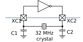
The crystal oscillator is designed for use with an AT-cut quartz crystal in parallel resonant mode, connected between pins XC1 and XC2. To achieve correct oscillation frequency, the load capacitance must match the specification in the crystal data sheet. The following figure shows how the 32 MHz crystal is connected to the high frequency crystal oscillator.
The load capacitance (CL) is the total capacitance seen by the crystal across its terminals and is calculated by the following equation.
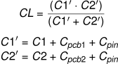
C1 and C2 are ceramic SMD capacitors connected between each crystal terminal and ground. For more information, see Reference circuitry. Cpcb1 and Cpcb2 are stray capacitance on the PCB. Cpin is the pin input capacitance on pins XC1 and XC2. See table 32 MHz crystal oscillator (HFXO). The load capacitors C1 and C2 should have the same value.
For reliable operation, the crystal load capacitance, shunt capacitance, equivalent series resistance, and drive level must comply with the specifications in table 32 MHz crystal oscillator (HFXO). It is recommended to use a crystal with lower than maximum load capacitance and/or shunt capacitance. A low load capacitance will reduce both startup time and current consumption.
Using internal capacitors
Optional internal capacitors ranging from 7.0 pF to 20.0 pF in 0.5 pF steps, are provided on pins XC1 and XC2.
Enabling internal capacitors eliminates the need for external capacitors for the 32 MHz crystal. The configuration of the internal capacitors must take place before starting the high-frequency crystal oscillator (HFXO).
The internal capacitors are used instead of the external capacitors C1 and C2, and the total capacitance seen by the crystal across its terminals is calculated by the load capacitance equation in High-frequency (32 MHz) crystal oscillator (HFXO).
CAPVALUE = (((FICR->XOSC32MTRIM.SLOPE+56)*(CAPACITANCE*2-14))
+((FICR->XOSC32MTRIM.OFFSET-8)<<4)+32)>>6;CAPACITANCEis the desired capacitor value in pF, holding any value between 7.0 pF and 20.0 pF in 0.5 pF steps.FICR->XOSC32MTRIMare factory trim values which usually are different from device to device.
After this, when HFXO is started, it will use the internal capacitor values together with the external crystal.
(CAPACITANCE*2-14) field of the above equation.Low-frequency (32.768 kHz) crystal oscillator (LFXO)
For higher LFCLK accuracy (when greater than ± 250 ppm accuracy is required), the 32.768 kHz crystal oscillator (LFXO) must be used.
To use the LFXO, a 32.768 kHz crystal must be connected between the XL1 and XL2 pins, as illustrated in the following figure.
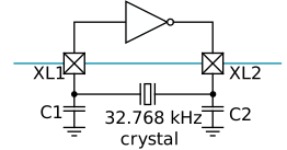
To enable oscillator functionality on XL1 and XL2 pins, use value Peripheral for the MCUSEL bitfield of the register PIN_CNF[n] (n=0..31) (Retained).
To achieve correct oscillation frequency, the load capacitance (CL) must match the specification in the crystal data sheet. The load capacitance (CL) is the total capacitance seen by the crystal across its terminals. It is calculated by the following equation.
C1 and C2 are ceramic SMD capacitors connected between each crystal terminal and ground. Cpcb1 and Cpcb2 are stray capacitance on the PCB. Cpin is the pin input capacitance on the XL1 and XL2 pins (see 32.768 kHz crystal oscillator (LFXO)). The load capacitors C1 and C2 should have the same value.
For more information, see Reference circuitry.
Using internal capacitors
Optional internal capacitors of 6 pF, 7 pF, and 9 pF are provided between pins XL1 and XL2.
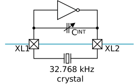
To enable this capacitor, choose the correct CINT capacitance in register XOSC32KI.INTCAP. The value of the internal capacitor CINT must match the specification in the crystal data sheet. CINT is the capacitance seen by the crystal across its terminals, including pin capacitance but excluding PCB stray capacitance.
Low-frequency (32.768 kHz) external source
The 32.768 kHz crystal oscillator (LFXO) is designed to work with external sources.
- A low swing clock. The signal should be applied to the XL1 pin with the XL2 pin grounded. Set OSCILLATORS.XOSC32KI.BYPASS=Disabled.
- A rail-to-rail clock. The signal should be applied to the XL1 pin with the XL2 pin left unconnected. Set OSCILLATORS.XOSC32KI.BYPASS=Enabled.
Registers
Instances
| Instance | Domain | Base address | TrustZone | Split access | Description | ||
|---|---|---|---|---|---|---|---|
| Map | Att | DMA | |||||
OSCILLATORS : S | APPLICATION | 0x50004000 | US | S | NA | No | Oscillator configuration |
Register overview
| Register | Offset | TZ | Description |
|---|---|---|---|
| XOSC32MCAPS | 0x5C4 | Programmable capacitance of XC1 and XC2 This register is retained. | |
| XOSC32KI.BYPASS | 0x6C0 | Enable or disable bypass of LFCLK crystal oscillator with external clock source This register is retained. | |
| XOSC32KI.INTCAP | 0x6D0 | Control usage of internal load capacitors This register is retained. |
XOSC32MCAPS (Retained)
Address offset: 0x5C4
Programmable capacitance of XC1 and XC2
This register is retained.
| Bit number | 31 | 30 | 29 | 28 | 27 | 26 | 25 | 24 | 23 | 22 | 21 | 20 | 19 | 18 | 17 | 16 | 15 | 14 | 13 | 12 | 11 | 10 | 9 | 8 | 7 | 6 | 5 | 4 | 3 | 2 | 1 | 0 | |||
|---|---|---|---|---|---|---|---|---|---|---|---|---|---|---|---|---|---|---|---|---|---|---|---|---|---|---|---|---|---|---|---|---|---|---|---|
| ID | B | A | A | A | A | A | |||||||||||||||||||||||||||||
| Reset 0x00000000 | 0 | 0 | 0 | 0 | 0 | 0 | 0 | 0 | 0 | 0 | 0 | 0 | 0 | 0 | 0 | 0 | 0 | 0 | 0 | 0 | 0 | 0 | 0 | 0 | 0 | 0 | 0 | 0 | 0 | 0 | 0 | 0 | |||
| ID | R/W | Field | Value ID | Value | Description | ||||||||||||||||||||||||||||||
| A | RW | CAPVALUE | Value representing capacitance, calculated using provided equation | ||||||||||||||||||||||||||||||||
| B | RW | ENABLE | Enable on-chip capacitors on XC1 and XC2 | ||||||||||||||||||||||||||||||||
Disabled | 0 | Capacitor disabled (use external caps) | |||||||||||||||||||||||||||||||||
Enabled | 1 | Capacitor enabled | |||||||||||||||||||||||||||||||||
XOSC32KI.BYPASS (Retained)
Address offset: 0x6C0
Enable or disable bypass of LFCLK crystal oscillator with external clock source
This register is retained.
| Bit number | 31 | 30 | 29 | 28 | 27 | 26 | 25 | 24 | 23 | 22 | 21 | 20 | 19 | 18 | 17 | 16 | 15 | 14 | 13 | 12 | 11 | 10 | 9 | 8 | 7 | 6 | 5 | 4 | 3 | 2 | 1 | 0 | |||
|---|---|---|---|---|---|---|---|---|---|---|---|---|---|---|---|---|---|---|---|---|---|---|---|---|---|---|---|---|---|---|---|---|---|---|---|
| ID | A | ||||||||||||||||||||||||||||||||||
| Reset 0x00000000 | 0 | 0 | 0 | 0 | 0 | 0 | 0 | 0 | 0 | 0 | 0 | 0 | 0 | 0 | 0 | 0 | 0 | 0 | 0 | 0 | 0 | 0 | 0 | 0 | 0 | 0 | 0 | 0 | 0 | 0 | 0 | 0 | |||
| ID | R/W | Field | Value ID | Value | Description | ||||||||||||||||||||||||||||||
| A | RW | BYPASS | Enable or disable bypass of LFCLK crystal oscillator with external clock source | ||||||||||||||||||||||||||||||||
Disabled | 0 | Disable (use with crystal or low-swing external source) | |||||||||||||||||||||||||||||||||
Enabled | 1 | Enable (use with rail-to-rail external source) | |||||||||||||||||||||||||||||||||
XOSC32KI.INTCAP (Retained)
Address offset: 0x6D0
Control usage of internal load capacitors
This register is retained.
| Bit number | 31 | 30 | 29 | 28 | 27 | 26 | 25 | 24 | 23 | 22 | 21 | 20 | 19 | 18 | 17 | 16 | 15 | 14 | 13 | 12 | 11 | 10 | 9 | 8 | 7 | 6 | 5 | 4 | 3 | 2 | 1 | 0 | |||
|---|---|---|---|---|---|---|---|---|---|---|---|---|---|---|---|---|---|---|---|---|---|---|---|---|---|---|---|---|---|---|---|---|---|---|---|
| ID | A | A | |||||||||||||||||||||||||||||||||
| Reset 0x00000000 | 0 | 0 | 0 | 0 | 0 | 0 | 0 | 0 | 0 | 0 | 0 | 0 | 0 | 0 | 0 | 0 | 0 | 0 | 0 | 0 | 0 | 0 | 0 | 0 | 0 | 0 | 0 | 0 | 0 | 0 | 0 | 0 | |||
| ID | R/W | Field | Value ID | Value | Description | ||||||||||||||||||||||||||||||
| A | RW | INTCAP | Control usage of internal load capacitors | ||||||||||||||||||||||||||||||||
External | 0 | Use external load capacitors | |||||||||||||||||||||||||||||||||
C6PF | 1 | 6 pF internal load capacitance | |||||||||||||||||||||||||||||||||
C7PF | 2 | 7 pF internal load capacitance | |||||||||||||||||||||||||||||||||
C9PF | 3 | 9 pF internal load capacitance | |||||||||||||||||||||||||||||||||
Electrical specification
32 MHz crystal oscillator (HFXO)
| Symbol | Description | Min. | Typ. | Max. | Units |
|---|---|---|---|---|---|
| fHFXO | External crystal frequency | 32 | MHz | ||
| fTOL_HFXO | Frequency tolerance requirement for 2.4 GHz proprietary radio applications | ±60 | ppm | ||
| fTOL_HFXO_BLE | Frequency tolerance requirement, Bluetooth Low Energy applications, packet length ≤ 200 bytes | ±40 | ppm | ||
| fTOL_HFXO_BLE_LP | Frequency tolerance requirement, Bluetooth Low Energy applications, packet length > 200 bytes | ±30 | ppm | ||
| CL_HFXO | Load capacitance | 6 | 8 | 12 | pF |
| C0_HFXO | Shunt capacitance | 7 | pF | ||
| RS_HFXO_7PF | Equivalent series resistance 3 pF < C0 <= 7 pF | 60 | Ω | ||
| RS_HFXO_3PF | Equivalent series resistance C0 <= 3 pF | 100 | Ω | ||
| PD_HFXO | Drive level | 100 | µW | ||
| CPIN_HFXO | Input capacitance XC1 and XC2 with internal capacitors disabled | 5.5 | pF | ||
| CPIN_HFXO_INT | Input capacitance XC1 and XC2 with internal capacitors enabled | 2.5 | pF | ||
| CHFXO_INT_MIN | Input capacitance XC1 and XC2, internal capacitor at minimum value, excluding CPIN_HFXO_INT | 7 | pF | ||
| CHFXO_INT_MAX | Input capacitance XC1 and XC2, internal capacitor at maximum value, excluding CPIN_HFXO_INT | 20 | pF | ||
| ISTBY_X32M | Core standby current for various crystals | ||||
| ISTBY_X32M_X0 | Typical parameters for a given 2.5mm x 2.0mm crystal: CL_HFXO = 8 pF, C0_HFXO = 1 pF, LM_HFXO = 7 mH, RS_HFXO = 20 Ω | 65 | µA | ||
| ISTBY_X32M_X1 | Typical parameters for a given 1.6mm x 1.2mm crystal: CL_HFXO = 8 pF, C0_HFXO = 0.4 pF, LM_HFXO = 20 mH, RS_HFXO = 40 Ω | 187 | µA | ||
| ISTBY_X32M_X2 | Typical parameters for a given 2.0mm x 1.6mm crystal: CL_HFXO = 8 pF, C0_HFXO = 0.73 pF, LM_HFXO = 9.47 mH, RS_HFXO = 16.32 Ω | 135 | µA | ||
| ISTBY_X32M_X3 | Typical parameters for a given 1.2mm x 1.0mm crystal: CL_HFXO = 8 pF, C0_HFXO = 0.42 pF, LM_HFXO = 22.7 mH, RS_HFXO = 100 Ω | 181 | µA | ||
| ISTART_X32M | Average startup current for various crystals, first 1 ms | ||||
| ISTART_X32M_X0 | Typical parameters for a given 2.5mm x 2.0mm crystal: CL_HFXO = 8 pF, C0_HFXO = 1 pF, LM_HFXO = 7 mH, RS_HFXO = 20 Ω | 363 | µA | ||
| ISTART_X32M_X1 | Typical parameters for a given 1.6mm x 1.2mm crystal: CL_HFXO = 8 pF, C0_HFXO = 0.4 pF, LM_HFXO = 20 mH, RS_HFXO = 40 Ω | 790 | µA | ||
| ISTART_X32M_X2 | Typical parameters for a given 2.0mm x 1.6mm crystal: CL_HFXO = 8 pF, C0_HFXO = 0.73 pF, LM_HFXO = 9.47 mH, RS_HFXO = 16.32 Ω | 467 | µA | ||
| ISTART_X32M_X3 | Typical parameters for a given 1.2mm x 1.0mm crystal: CL_HFXO = 8 pF, C0_HFXO = 0.42 pF, LM_HFXO = 22.7 mH, RS_HFXO = 100 Ω | 863 | µA | ||
| tPOWERUP_X32M | Power-up time for various crystals | ||||
| tPOWERUP_X32M_X0 | Typical parameters for a given 2.5mm x 2.0mm crystal: CL_HFXO = 8 pF, C0_HFXO = 1 pF, LM_HFXO = 7 mH, RS_HFXO = 20 Ω | 60 | µs | ||
| tPOWERUP_X32M_X1 | Typical parameters for a given 1.6mm x 1.2mm crystal: CL_HFXO = 8 pF, C0_HFXO = 0.4 pF, LM_HFXO = 20 mH, RS_HFXO = 40 Ω | 187 | µs | ||
| tPOWERUP_X32M_X2 | Typical parameters for a given 2.0mm x 1.6mm crystal: CL_HFXO = 8 pF, C0_HFXO = 0.73 pF, LM_HFXO = 9.47 mH, RS_HFXO = 16.32 Ω | 60 | µs | ||
| tPOWERUP_X32M_X3 | Typical parameters for a given 1.2mm x 1.0mm crystal: CL_HFXO = 8 pF, C0_HFXO = 0.42 pF, LM_HFXO = 22.7 mH, RS_HFXO = 100 Ω | 211 | µs |
32.768 kHz crystal oscillator (LFXO)
| Symbol | Description | Min. | Typ. | Max. | Units |
|---|---|---|---|---|---|
| fLFXO | External crystal frequency | 32.768 | kHz | ||
| fTOL_LFXO_BLE | Frequency tolerance requirement, Bluetooth Low Energy applications | ±500 | ppm | ||
| fTOL_LFXO_ANT | Frequency tolerance requirement for ANT applications | ±50 | ppm | ||
| CL_LFXO | Load capacitance | 7 | 9 | pF | |
| C0_LFXO | Shunt capacitance | 1 | 2 | pF | |
| RS_LFXO | Equivalent series resistance | 60 | 90 | kΩ | |
| PD_LFXO | Drive level | 0.5 | μW | ||
| Cpin | Input capacitance on XL1 and XL2 pads when internal capacitor is disabled | 4 | pF | ||
| Cpin | Total capacitance between XL1 and XL2 pads when internal capacitor enabled | 6 | 7 | 9 | pF |
| VAMP,IN,XO,LOW | Peak-to-peak amplitude for external low swing clock. Input signal must not swing outside supply rails. | 200 | 1000 | mV |