CACHE — Instruction/data cache
The cache is two-way set associative with a least recently used (LRU) replacement policy. Both instruction and data accesses towards flash memory or XIP code regions are cached.
- 128-bit cache line
- Configurable as a cache or general purpose RAM
- Hit/miss counters per NVM region and access type (instruction or data)
- Readable cache content (for profiling)
- Data, tag, valid, and most recently used (MRU) bits
- Can be disabled when not in use
- Manual invalidation and erase support
- Locking cache updates on cache misses
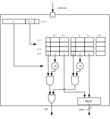
In Cache mode (MODE=Cache), instruction and data accesses from the CPU over the code bus towards internal or external flash, are cached. The contents of the cache, i.e. data, tag, valid, and MRU bits, are memory mapped, see Cache content. This can be used for performance profiling of code running in the system. Access to the cache content region is read-only by default, but can be blocked by enabling a lock bit in DEBUGLOCK. Preventing cache content updates on cache misses can be enabled through register DEBUGLOCK. When enabled, cache content is not replaced, but kept intact. The cache is still enabled and provides fast instruction and data fetches for cached content.
Access to internal or external flash memory will not be cached when in Ram mode (MODE=Ram). Instead, the cache data content, as described in Cache content, can be used as read/write RAM.
Cache content
Cache information is divided into cache info content and cache data content.
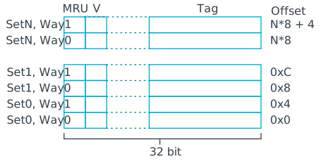
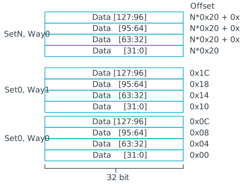
The cache info and cache data content are memory mapped in the CACHEINFO and CACHEDATA regions. These can be accessed in the CACHEINFO registers and CACHEDATA registers respectively.
Profiling
The cache includes profiling counters IHIT, IMISS, DHIT, and DMISS for both flash and execute-in-place (XIP).
Cache performance on executed code is indicated by these counters when enabled through PROFILINGENABLE. The counters can be cleared at any time using PROFILINGCLEAR. Writing to this register will clear all profiling counters. After being cleared, the counters will increment at the next instruction, or data fetch, according to the rules in the following table.
| Profiling counter | Description |
|---|---|
| IHIT | Increased on a cache hit for instruction fetch |
| IMISS | Increased on a cache miss for instruction fetch |
| DHIT | Increased on a cache hit for data fetch (i.e. LOAD type instruction targeting the cache region) |
| DMISS | Increased on a cache miss for data fetch (i.e. LOAD type instruction targeting the cache region) |
Registers
Instances
| Instance | Domain | Base address | TrustZone | Split access | Description | ||
|---|---|---|---|---|---|---|---|
| Map | Att | DMA | |||||
| CACHE | APPLICATION | 0x50001000 | HF | S | NA | No | Cache |
Register overview
| Register | Offset | TZ | Description |
|---|---|---|---|
| PROFILING[n].IHIT | 0x400 | Instruction fetch cache hit counter for cache region n, where n=0 means Flash and n=1 means XIP. | |
| PROFILING[n].IMISS | 0x404 | Instruction fetch cache miss counter for cache region n, where n=0 means Flash and n=1 means XIP. | |
| PROFILING[n].DHIT | 0x408 | Data fetch cache hit counter for cache region n, where n=0 means Flash and n=1 means XIP. | |
| PROFILING[n].DMISS | 0x40C | Data fetch cache miss counter for cache region n, where n=0 means Flash and n=1 means XIP. | |
| ENABLE | 0x500 | Enable cache. | |
| INVALIDATE | 0x504 | Invalidate the cache. | |
| ERASE | 0x508 | Erase the cache. | |
| PROFILINGENABLE | 0x50C | Enable the profiling counters. | |
| PROFILINGCLEAR | 0x510 | Clear the profiling counters. | |
| MODE | 0x514 | Cache mode. Switching from Cache to Ram mode causes the RAM to be cleared. Switching from RAM to Cache mode causes the cache to be invalidated. | |
| DEBUGLOCK | 0x518 | Lock debug mode. | |
| ERASESTATUS | 0x51C | Cache erase status. | |
| WRITELOCK | 0x520 | Lock cache updates. Prevents updating of cache content on cache misses, but will continue to lookup instruction/data fetches in content already present in the cache. Ignored in RAM mode. |
PROFILING[n].IHIT (n=0..1)
Address offset: 0x400 + (n × 0x20)
Instruction fetch cache hit counter for cache region n, where n=0 means Flash and n=1 means XIP.
| Bit number | 31 | 30 | 29 | 28 | 27 | 26 | 25 | 24 | 23 | 22 | 21 | 20 | 19 | 18 | 17 | 16 | 15 | 14 | 13 | 12 | 11 | 10 | 9 | 8 | 7 | 6 | 5 | 4 | 3 | 2 | 1 | 0 | |||
|---|---|---|---|---|---|---|---|---|---|---|---|---|---|---|---|---|---|---|---|---|---|---|---|---|---|---|---|---|---|---|---|---|---|---|---|
| ID | A | A | A | A | A | A | A | A | A | A | A | A | A | A | A | A | A | A | A | A | A | A | A | A | A | A | A | A | A | A | A | A | |||
| Reset 0x00000000 | 0 | 0 | 0 | 0 | 0 | 0 | 0 | 0 | 0 | 0 | 0 | 0 | 0 | 0 | 0 | 0 | 0 | 0 | 0 | 0 | 0 | 0 | 0 | 0 | 0 | 0 | 0 | 0 | 0 | 0 | 0 | 0 | |||
| ID | R/W | Field | Value ID | Value | Description | ||||||||||||||||||||||||||||||
| A | R | HITS | Number of instruction cache hits | ||||||||||||||||||||||||||||||||
PROFILING[n].IMISS (n=0..1)
Address offset: 0x404 + (n × 0x20)
Instruction fetch cache miss counter for cache region n, where n=0 means Flash and n=1 means XIP.
| Bit number | 31 | 30 | 29 | 28 | 27 | 26 | 25 | 24 | 23 | 22 | 21 | 20 | 19 | 18 | 17 | 16 | 15 | 14 | 13 | 12 | 11 | 10 | 9 | 8 | 7 | 6 | 5 | 4 | 3 | 2 | 1 | 0 | |||
|---|---|---|---|---|---|---|---|---|---|---|---|---|---|---|---|---|---|---|---|---|---|---|---|---|---|---|---|---|---|---|---|---|---|---|---|
| ID | A | A | A | A | A | A | A | A | A | A | A | A | A | A | A | A | A | A | A | A | A | A | A | A | A | A | A | A | A | A | A | A | |||
| Reset 0x00000000 | 0 | 0 | 0 | 0 | 0 | 0 | 0 | 0 | 0 | 0 | 0 | 0 | 0 | 0 | 0 | 0 | 0 | 0 | 0 | 0 | 0 | 0 | 0 | 0 | 0 | 0 | 0 | 0 | 0 | 0 | 0 | 0 | |||
| ID | R/W | Field | Value ID | Value | Description | ||||||||||||||||||||||||||||||
| A | R | MISSES | Number of instruction cache misses | ||||||||||||||||||||||||||||||||
PROFILING[n].DHIT (n=0..1)
Address offset: 0x408 + (n × 0x20)
Data fetch cache hit counter for cache region n, where n=0 means Flash and n=1 means XIP.
| Bit number | 31 | 30 | 29 | 28 | 27 | 26 | 25 | 24 | 23 | 22 | 21 | 20 | 19 | 18 | 17 | 16 | 15 | 14 | 13 | 12 | 11 | 10 | 9 | 8 | 7 | 6 | 5 | 4 | 3 | 2 | 1 | 0 | |||
|---|---|---|---|---|---|---|---|---|---|---|---|---|---|---|---|---|---|---|---|---|---|---|---|---|---|---|---|---|---|---|---|---|---|---|---|
| ID | A | A | A | A | A | A | A | A | A | A | A | A | A | A | A | A | A | A | A | A | A | A | A | A | A | A | A | A | A | A | A | A | |||
| Reset 0x00000000 | 0 | 0 | 0 | 0 | 0 | 0 | 0 | 0 | 0 | 0 | 0 | 0 | 0 | 0 | 0 | 0 | 0 | 0 | 0 | 0 | 0 | 0 | 0 | 0 | 0 | 0 | 0 | 0 | 0 | 0 | 0 | 0 | |||
| ID | R/W | Field | Value ID | Value | Description | ||||||||||||||||||||||||||||||
| A | R | HITS | Number of data cache hits | ||||||||||||||||||||||||||||||||
PROFILING[n].DMISS (n=0..1)
Address offset: 0x40C + (n × 0x20)
Data fetch cache miss counter for cache region n, where n=0 means Flash and n=1 means XIP.
| Bit number | 31 | 30 | 29 | 28 | 27 | 26 | 25 | 24 | 23 | 22 | 21 | 20 | 19 | 18 | 17 | 16 | 15 | 14 | 13 | 12 | 11 | 10 | 9 | 8 | 7 | 6 | 5 | 4 | 3 | 2 | 1 | 0 | |||
|---|---|---|---|---|---|---|---|---|---|---|---|---|---|---|---|---|---|---|---|---|---|---|---|---|---|---|---|---|---|---|---|---|---|---|---|
| ID | A | A | A | A | A | A | A | A | A | A | A | A | A | A | A | A | A | A | A | A | A | A | A | A | A | A | A | A | A | A | A | A | |||
| Reset 0x00000000 | 0 | 0 | 0 | 0 | 0 | 0 | 0 | 0 | 0 | 0 | 0 | 0 | 0 | 0 | 0 | 0 | 0 | 0 | 0 | 0 | 0 | 0 | 0 | 0 | 0 | 0 | 0 | 0 | 0 | 0 | 0 | 0 | |||
| ID | R/W | Field | Value ID | Value | Description | ||||||||||||||||||||||||||||||
| A | R | MISSES | Number of data cache misses | ||||||||||||||||||||||||||||||||
ENABLE
Address offset: 0x500
Enable cache.
| Bit number | 31 | 30 | 29 | 28 | 27 | 26 | 25 | 24 | 23 | 22 | 21 | 20 | 19 | 18 | 17 | 16 | 15 | 14 | 13 | 12 | 11 | 10 | 9 | 8 | 7 | 6 | 5 | 4 | 3 | 2 | 1 | 0 | |||
|---|---|---|---|---|---|---|---|---|---|---|---|---|---|---|---|---|---|---|---|---|---|---|---|---|---|---|---|---|---|---|---|---|---|---|---|
| ID | A | ||||||||||||||||||||||||||||||||||
| Reset 0x00000000 | 0 | 0 | 0 | 0 | 0 | 0 | 0 | 0 | 0 | 0 | 0 | 0 | 0 | 0 | 0 | 0 | 0 | 0 | 0 | 0 | 0 | 0 | 0 | 0 | 0 | 0 | 0 | 0 | 0 | 0 | 0 | 0 | |||
| ID | R/W | Field | Value ID | Value | Description | ||||||||||||||||||||||||||||||
| A | RW | ENABLE | Enable cache | ||||||||||||||||||||||||||||||||
Disabled | 0 | Disable cache | |||||||||||||||||||||||||||||||||
Enabled | 1 | Enable cache | |||||||||||||||||||||||||||||||||
INVALIDATE
Address offset: 0x504
Invalidate the cache.
| Bit number | 31 | 30 | 29 | 28 | 27 | 26 | 25 | 24 | 23 | 22 | 21 | 20 | 19 | 18 | 17 | 16 | 15 | 14 | 13 | 12 | 11 | 10 | 9 | 8 | 7 | 6 | 5 | 4 | 3 | 2 | 1 | 0 | |||
|---|---|---|---|---|---|---|---|---|---|---|---|---|---|---|---|---|---|---|---|---|---|---|---|---|---|---|---|---|---|---|---|---|---|---|---|
| ID | A | ||||||||||||||||||||||||||||||||||
| Reset 0x00000000 | 0 | 0 | 0 | 0 | 0 | 0 | 0 | 0 | 0 | 0 | 0 | 0 | 0 | 0 | 0 | 0 | 0 | 0 | 0 | 0 | 0 | 0 | 0 | 0 | 0 | 0 | 0 | 0 | 0 | 0 | 0 | 0 | |||
| ID | R/W | Field | Value ID | Value | Description | ||||||||||||||||||||||||||||||
| A | W | INVALIDATE | Invalidate the cache | ||||||||||||||||||||||||||||||||
Invalidate | 1 | Invalidate the cache | |||||||||||||||||||||||||||||||||
ERASE
Address offset: 0x508
Erase the cache.
| Bit number | 31 | 30 | 29 | 28 | 27 | 26 | 25 | 24 | 23 | 22 | 21 | 20 | 19 | 18 | 17 | 16 | 15 | 14 | 13 | 12 | 11 | 10 | 9 | 8 | 7 | 6 | 5 | 4 | 3 | 2 | 1 | 0 | |||
|---|---|---|---|---|---|---|---|---|---|---|---|---|---|---|---|---|---|---|---|---|---|---|---|---|---|---|---|---|---|---|---|---|---|---|---|
| ID | A | ||||||||||||||||||||||||||||||||||
| Reset 0x00000000 | 0 | 0 | 0 | 0 | 0 | 0 | 0 | 0 | 0 | 0 | 0 | 0 | 0 | 0 | 0 | 0 | 0 | 0 | 0 | 0 | 0 | 0 | 0 | 0 | 0 | 0 | 0 | 0 | 0 | 0 | 0 | 0 | |||
| ID | R/W | Field | Value ID | Value | Description | ||||||||||||||||||||||||||||||
| A | W | ERASE | Erase the cache | ||||||||||||||||||||||||||||||||
Erase | 1 | Erase cache | |||||||||||||||||||||||||||||||||
PROFILINGENABLE
Address offset: 0x50C
Enable the profiling counters.
| Bit number | 31 | 30 | 29 | 28 | 27 | 26 | 25 | 24 | 23 | 22 | 21 | 20 | 19 | 18 | 17 | 16 | 15 | 14 | 13 | 12 | 11 | 10 | 9 | 8 | 7 | 6 | 5 | 4 | 3 | 2 | 1 | 0 | |||
|---|---|---|---|---|---|---|---|---|---|---|---|---|---|---|---|---|---|---|---|---|---|---|---|---|---|---|---|---|---|---|---|---|---|---|---|
| ID | A | ||||||||||||||||||||||||||||||||||
| Reset 0x00000000 | 0 | 0 | 0 | 0 | 0 | 0 | 0 | 0 | 0 | 0 | 0 | 0 | 0 | 0 | 0 | 0 | 0 | 0 | 0 | 0 | 0 | 0 | 0 | 0 | 0 | 0 | 0 | 0 | 0 | 0 | 0 | 0 | |||
| ID | R/W | Field | Value ID | Value | Description | ||||||||||||||||||||||||||||||
| A | RW | ENABLE | Enable the profiling counters | ||||||||||||||||||||||||||||||||
Disable | 0 | Disable profiling | |||||||||||||||||||||||||||||||||
Enable | 1 | Enable profiling | |||||||||||||||||||||||||||||||||
PROFILINGCLEAR
Address offset: 0x510
Clear the profiling counters.
The profiling counters can be cleared at any time. When cleared, all profiling counters will be set to zero, and will increment at the next instruction or data fetch.
| Bit number | 31 | 30 | 29 | 28 | 27 | 26 | 25 | 24 | 23 | 22 | 21 | 20 | 19 | 18 | 17 | 16 | 15 | 14 | 13 | 12 | 11 | 10 | 9 | 8 | 7 | 6 | 5 | 4 | 3 | 2 | 1 | 0 | |||
|---|---|---|---|---|---|---|---|---|---|---|---|---|---|---|---|---|---|---|---|---|---|---|---|---|---|---|---|---|---|---|---|---|---|---|---|
| ID | A | ||||||||||||||||||||||||||||||||||
| Reset 0x00000000 | 0 | 0 | 0 | 0 | 0 | 0 | 0 | 0 | 0 | 0 | 0 | 0 | 0 | 0 | 0 | 0 | 0 | 0 | 0 | 0 | 0 | 0 | 0 | 0 | 0 | 0 | 0 | 0 | 0 | 0 | 0 | 0 | |||
| ID | R/W | Field | Value ID | Value | Description | ||||||||||||||||||||||||||||||
| A | W | CLEAR | Clearing the profiling counters | ||||||||||||||||||||||||||||||||
Clear | 1 | Clear the profiling counters | |||||||||||||||||||||||||||||||||
MODE
Address offset: 0x514
Cache mode.
Switching from Cache to Ram mode causes the RAM to be cleared.
Switching from RAM to Cache mode causes the cache to be invalidated.
| Bit number | 31 | 30 | 29 | 28 | 27 | 26 | 25 | 24 | 23 | 22 | 21 | 20 | 19 | 18 | 17 | 16 | 15 | 14 | 13 | 12 | 11 | 10 | 9 | 8 | 7 | 6 | 5 | 4 | 3 | 2 | 1 | 0 | |||
|---|---|---|---|---|---|---|---|---|---|---|---|---|---|---|---|---|---|---|---|---|---|---|---|---|---|---|---|---|---|---|---|---|---|---|---|
| ID | A | ||||||||||||||||||||||||||||||||||
| Reset 0x00000000 | 0 | 0 | 0 | 0 | 0 | 0 | 0 | 0 | 0 | 0 | 0 | 0 | 0 | 0 | 0 | 0 | 0 | 0 | 0 | 0 | 0 | 0 | 0 | 0 | 0 | 0 | 0 | 0 | 0 | 0 | 0 | 0 | |||
| ID | R/W | Field | Value ID | Value | Description | ||||||||||||||||||||||||||||||
| A | RW | MODE | Cache mode | ||||||||||||||||||||||||||||||||
Cache | 0 | Cache mode | |||||||||||||||||||||||||||||||||
Ram | 1 | RAM mode | |||||||||||||||||||||||||||||||||
DEBUGLOCK
Address offset: 0x518
Lock debug mode.
This register is ignored when CACHE is used in RAM mode. Once this register has been set to Locked, the debug mode can only be unlocked by resetting the device.
| Bit number | 31 | 30 | 29 | 28 | 27 | 26 | 25 | 24 | 23 | 22 | 21 | 20 | 19 | 18 | 17 | 16 | 15 | 14 | 13 | 12 | 11 | 10 | 9 | 8 | 7 | 6 | 5 | 4 | 3 | 2 | 1 | 0 | |||
|---|---|---|---|---|---|---|---|---|---|---|---|---|---|---|---|---|---|---|---|---|---|---|---|---|---|---|---|---|---|---|---|---|---|---|---|
| ID | A | ||||||||||||||||||||||||||||||||||
| Reset 0x00000000 | 0 | 0 | 0 | 0 | 0 | 0 | 0 | 0 | 0 | 0 | 0 | 0 | 0 | 0 | 0 | 0 | 0 | 0 | 0 | 0 | 0 | 0 | 0 | 0 | 0 | 0 | 0 | 0 | 0 | 0 | 0 | 0 | |||
| ID | R/W | Field | Value ID | Value | Description | ||||||||||||||||||||||||||||||
| A | RW1 | DEBUGLOCK | Lock debug mode | ||||||||||||||||||||||||||||||||
Unlocked | 0 | Debug mode unlocked | |||||||||||||||||||||||||||||||||
Locked | 1 | Debug mode locked | |||||||||||||||||||||||||||||||||
ERASESTATUS
Address offset: 0x51C
Cache erase status.
| Bit number | 31 | 30 | 29 | 28 | 27 | 26 | 25 | 24 | 23 | 22 | 21 | 20 | 19 | 18 | 17 | 16 | 15 | 14 | 13 | 12 | 11 | 10 | 9 | 8 | 7 | 6 | 5 | 4 | 3 | 2 | 1 | 0 | |||
|---|---|---|---|---|---|---|---|---|---|---|---|---|---|---|---|---|---|---|---|---|---|---|---|---|---|---|---|---|---|---|---|---|---|---|---|
| ID | A | ||||||||||||||||||||||||||||||||||
| Reset 0x00000000 | 0 | 0 | 0 | 0 | 0 | 0 | 0 | 0 | 0 | 0 | 0 | 0 | 0 | 0 | 0 | 0 | 0 | 0 | 0 | 0 | 0 | 0 | 0 | 0 | 0 | 0 | 0 | 0 | 0 | 0 | 0 | 0 | |||
| ID | R/W | Field | Value ID | Value | Description | ||||||||||||||||||||||||||||||
| A | RW | ERASESTATUS | Cache erase status | ||||||||||||||||||||||||||||||||
Idle | 0 | Erase is not complete or hasn't started | |||||||||||||||||||||||||||||||||
Finished | 1 | Cache erase is finished Write 0 to clear. | |||||||||||||||||||||||||||||||||
WRITELOCK
Address offset: 0x520
Lock cache updates. Prevents updating of cache content on cache misses, but will continue to lookup instruction/data fetches in content already present in the cache.
Ignored in RAM mode.
| Bit number | 31 | 30 | 29 | 28 | 27 | 26 | 25 | 24 | 23 | 22 | 21 | 20 | 19 | 18 | 17 | 16 | 15 | 14 | 13 | 12 | 11 | 10 | 9 | 8 | 7 | 6 | 5 | 4 | 3 | 2 | 1 | 0 | |||
|---|---|---|---|---|---|---|---|---|---|---|---|---|---|---|---|---|---|---|---|---|---|---|---|---|---|---|---|---|---|---|---|---|---|---|---|
| ID | A | ||||||||||||||||||||||||||||||||||
| Reset 0x00000000 | 0 | 0 | 0 | 0 | 0 | 0 | 0 | 0 | 0 | 0 | 0 | 0 | 0 | 0 | 0 | 0 | 0 | 0 | 0 | 0 | 0 | 0 | 0 | 0 | 0 | 0 | 0 | 0 | 0 | 0 | 0 | 0 | |||
| ID | R/W | Field | Value ID | Value | Description | ||||||||||||||||||||||||||||||
| A | RW | WRITELOCK | Lock cache updates | ||||||||||||||||||||||||||||||||
Unlocked | 0 | Cache updates unlocked | |||||||||||||||||||||||||||||||||
Locked | 1 | Cache updates locked | |||||||||||||||||||||||||||||||||
Electrical specification
Cache size
| Symbol | Description | Min. | Typ. | Max. | Units |
|---|---|---|---|---|---|
| SizeCACHEDATA | CACHEDATA size | 8192 | Bytes |
Registers
Instances
| Instance | Domain | Base address | TrustZone | Split access | Description | ||
|---|---|---|---|---|---|---|---|
| Map | Att | DMA | |||||
| CACHEINFO | APPLICATION | 0x00F08000 | HF | S | NA | No | Cache info |
Register overview
| Register | Offset | TZ | Description |
|---|---|---|---|
| SET[n].WAY[o] | 0x0 | Cache information for SET[n], WAY[o]. |
SET[n].WAY[o] (n=0..255) (o=0..1)
Address offset: 0x0 + (n × 0x8) + (o × 0x4)
Cache information for SET[n], WAY[o].
| Bit number | 31 | 30 | 29 | 28 | 27 | 26 | 25 | 24 | 23 | 22 | 21 | 20 | 19 | 18 | 17 | 16 | 15 | 14 | 13 | 12 | 11 | 10 | 9 | 8 | 7 | 6 | 5 | 4 | 3 | 2 | 1 | 0 | |||
|---|---|---|---|---|---|---|---|---|---|---|---|---|---|---|---|---|---|---|---|---|---|---|---|---|---|---|---|---|---|---|---|---|---|---|---|
| ID | C | B | A | A | A | A | A | A | A | A | A | A | A | A | A | A | A | A | A | ||||||||||||||||
| Reset 0x00000000 | 0 | 0 | 0 | 0 | 0 | 0 | 0 | 0 | 0 | 0 | 0 | 0 | 0 | 0 | 0 | 0 | 0 | 0 | 0 | 0 | 0 | 0 | 0 | 0 | 0 | 0 | 0 | 0 | 0 | 0 | 0 | 0 | |||
| ID | R/W | Field | Value ID | Value | Description | ||||||||||||||||||||||||||||||
| A | RW | TAG | Cache tag. | ||||||||||||||||||||||||||||||||
| B | R | V | Valid bit | ||||||||||||||||||||||||||||||||
Invalid | 0 | Invalid cache line | |||||||||||||||||||||||||||||||||
Valid | 1 | Valid cache line | |||||||||||||||||||||||||||||||||
| C | R | MRU | Most recently used way. | ||||||||||||||||||||||||||||||||
Way0 | 0 | Way0 was most recently used | |||||||||||||||||||||||||||||||||
Way1 | 1 | Way1 was most recently used | |||||||||||||||||||||||||||||||||
Registers
Instances
| Instance | Domain | Base address | TrustZone | Split access | Description | ||
|---|---|---|---|---|---|---|---|
| Map | Att | DMA | |||||
| CACHEDATA | APPLICATION | 0x00F00000 | HF | S | NA | No | Cache data |
Register overview
| Register | Offset | TZ | Description |
|---|---|---|---|
| SET[n].WAY[o].DATA0 | 0x0 | Cache data bits [31:0] of SET[n], WAY[o]. | |
| SET[n].WAY[o].DATA1 | 0x4 | Cache data bits [63:32] of SET[n], WAY[o]. | |
| SET[n].WAY[o].DATA2 | 0x8 | Cache data bits [95:64] of SET[n], WAY[o]. | |
| SET[n].WAY[o].DATA3 | 0xC | Cache data bits [127:96] of SET[n], WAY[o]. |
SET[n].WAY[o].DATA0 (n=0..255) (o=0..1)
Address offset: 0x0 + (n × 0x20) + (o × 0x10)
Cache data bits [31:0] of SET[n], WAY[o].
| Bit number | 31 | 30 | 29 | 28 | 27 | 26 | 25 | 24 | 23 | 22 | 21 | 20 | 19 | 18 | 17 | 16 | 15 | 14 | 13 | 12 | 11 | 10 | 9 | 8 | 7 | 6 | 5 | 4 | 3 | 2 | 1 | 0 | |||
|---|---|---|---|---|---|---|---|---|---|---|---|---|---|---|---|---|---|---|---|---|---|---|---|---|---|---|---|---|---|---|---|---|---|---|---|
| ID | A | A | A | A | A | A | A | A | A | A | A | A | A | A | A | A | A | A | A | A | A | A | A | A | A | A | A | A | A | A | A | A | |||
| Reset 0x00000000 | 0 | 0 | 0 | 0 | 0 | 0 | 0 | 0 | 0 | 0 | 0 | 0 | 0 | 0 | 0 | 0 | 0 | 0 | 0 | 0 | 0 | 0 | 0 | 0 | 0 | 0 | 0 | 0 | 0 | 0 | 0 | 0 | |||
| ID | R/W | Field | Value ID | Value | Description | ||||||||||||||||||||||||||||||
| A | RW | Data | Data | ||||||||||||||||||||||||||||||||
SET[n].WAY[o].DATA1 (n=0..255) (o=0..1)
Address offset: 0x4 + (n × 0x20) + (o × 0x10)
Cache data bits [63:32] of SET[n], WAY[o].
| Bit number | 31 | 30 | 29 | 28 | 27 | 26 | 25 | 24 | 23 | 22 | 21 | 20 | 19 | 18 | 17 | 16 | 15 | 14 | 13 | 12 | 11 | 10 | 9 | 8 | 7 | 6 | 5 | 4 | 3 | 2 | 1 | 0 | |||
|---|---|---|---|---|---|---|---|---|---|---|---|---|---|---|---|---|---|---|---|---|---|---|---|---|---|---|---|---|---|---|---|---|---|---|---|
| ID | A | A | A | A | A | A | A | A | A | A | A | A | A | A | A | A | A | A | A | A | A | A | A | A | A | A | A | A | A | A | A | A | |||
| Reset 0x00000000 | 0 | 0 | 0 | 0 | 0 | 0 | 0 | 0 | 0 | 0 | 0 | 0 | 0 | 0 | 0 | 0 | 0 | 0 | 0 | 0 | 0 | 0 | 0 | 0 | 0 | 0 | 0 | 0 | 0 | 0 | 0 | 0 | |||
| ID | R/W | Field | Value ID | Value | Description | ||||||||||||||||||||||||||||||
| A | RW | Data | Data | ||||||||||||||||||||||||||||||||
SET[n].WAY[o].DATA2 (n=0..255) (o=0..1)
Address offset: 0x8 + (n × 0x20) + (o × 0x10)
Cache data bits [95:64] of SET[n], WAY[o].
| Bit number | 31 | 30 | 29 | 28 | 27 | 26 | 25 | 24 | 23 | 22 | 21 | 20 | 19 | 18 | 17 | 16 | 15 | 14 | 13 | 12 | 11 | 10 | 9 | 8 | 7 | 6 | 5 | 4 | 3 | 2 | 1 | 0 | |||
|---|---|---|---|---|---|---|---|---|---|---|---|---|---|---|---|---|---|---|---|---|---|---|---|---|---|---|---|---|---|---|---|---|---|---|---|
| ID | A | A | A | A | A | A | A | A | A | A | A | A | A | A | A | A | A | A | A | A | A | A | A | A | A | A | A | A | A | A | A | A | |||
| Reset 0x00000000 | 0 | 0 | 0 | 0 | 0 | 0 | 0 | 0 | 0 | 0 | 0 | 0 | 0 | 0 | 0 | 0 | 0 | 0 | 0 | 0 | 0 | 0 | 0 | 0 | 0 | 0 | 0 | 0 | 0 | 0 | 0 | 0 | |||
| ID | R/W | Field | Value ID | Value | Description | ||||||||||||||||||||||||||||||
| A | RW | Data | Data | ||||||||||||||||||||||||||||||||
SET[n].WAY[o].DATA3 (n=0..255) (o=0..1)
Address offset: 0xC + (n × 0x20) + (o × 0x10)
Cache data bits [127:96] of SET[n], WAY[o].
| Bit number | 31 | 30 | 29 | 28 | 27 | 26 | 25 | 24 | 23 | 22 | 21 | 20 | 19 | 18 | 17 | 16 | 15 | 14 | 13 | 12 | 11 | 10 | 9 | 8 | 7 | 6 | 5 | 4 | 3 | 2 | 1 | 0 | |||
|---|---|---|---|---|---|---|---|---|---|---|---|---|---|---|---|---|---|---|---|---|---|---|---|---|---|---|---|---|---|---|---|---|---|---|---|
| ID | A | A | A | A | A | A | A | A | A | A | A | A | A | A | A | A | A | A | A | A | A | A | A | A | A | A | A | A | A | A | A | A | |||
| Reset 0x00000000 | 0 | 0 | 0 | 0 | 0 | 0 | 0 | 0 | 0 | 0 | 0 | 0 | 0 | 0 | 0 | 0 | 0 | 0 | 0 | 0 | 0 | 0 | 0 | 0 | 0 | 0 | 0 | 0 | 0 | 0 | 0 | 0 | |||
| ID | R/W | Field | Value ID | Value | Description | ||||||||||||||||||||||||||||||
| A | RW | Data | Data | ||||||||||||||||||||||||||||||||