QSPI — Quad serial peripheral interface
The QSPI peripheral provides support for communicating with an external flash memory device using SPI.
The main features for the QSPI peripheral are:
- Single/dual/quad SPI input/output
- 6 to 96 MHz configurable clock frequency
- Single-word read/write access from/to external flash
- EasyDMA for block read and write transfers
- Up to 48 MB/sec EasyDMA read rate
- Execute in place (XIP) for executing program directly from external flash
- XIP access can optionally be disabled
- On-the-fly encryption and decryption, including EasyDMA and XIP
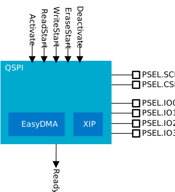
Configuring QSPI
Before any data can be transferred to or from the external flash memory, the peripheral needs to be configured.
If the IFCONFIG0 register is configured to use the quad mode, the external flash device also needs to be set in the quad mode before any data transfers can take place.
This can be done by sending custom instructions to the external flash device, as described in Sending custom instructions.
Write operation
A write operation to the external flash is configured using the WRITE.DST, WRITE.SRC, and WRITE.CNT registers. It is started using the WRITESTART task.
The READY event is generated when the transfer is complete.
The QSPI peripheral automatically takes care of splitting DMA transfers into page writes.
Read operation
Erase operation
Erase of pages/blocks of the external flash is configured using the ERASE.PTR and ERASE.LEN registers. It is started using the ERASESTART task.
The READY event is generated when the erase operation has been started.
In this case, the READY event will not indicate that the erase operation of the flash has been completed, but it only signals that the erase operation has been started. The actual status of the erase operation can normally be read from the external flash using a custom instruction (see Sending custom instructions).
Execute in place
Execute in place (XIP) allows the CPU to execute program code directly from the external flash.
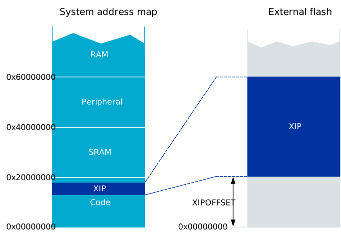
After the external flash has been configured, the CPU can execute code from the external flash by accessing the XIP memory region. See the following figure and Memory for details.
The XIP memory region is read-only, writing to it will result in a bus error.
When accessing the XIP memory region, the start address of this XIP memory region will map to the address XIPOFFSET of the external flash.
Encryption
The contents of an external flash memory can be protected using stream cipher encryption. Encryption can be configured and enabled independently for XIP and EasyDMA, with separate keys and nonce.
Once configured and enabled, the stream cipher operates between the AHB bus and the external flash, encrypting and decrypting data passing through.
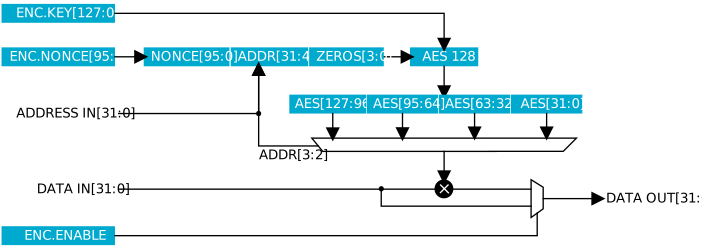
The same nonce and key must be used for both encryption and decryption of the same memory address.
The memory address used for encryption is the external flash memory address and thus independent of XIPOFFSET. This means a second firmware image can be encrypted and written using EasyDMA, then XIPOFFSET set to point to the new firmware image before executing from it.
Stream ciphers are symmetric. They do not differentiate between encrypting or decrypting, reading or writing. Thus, if the contents of a plain text external flash is read when stream cipher is enabled, the data provided to the MCU is encrypted.
Execute in place (XIP)
- Configure keys using XIP_ENC.KEY0 through XIP_ENC.KEY3.
- Configure nonce using XIP_ENC.NONCE0 through XIP_ENC.NONCE2.
- Set XIP_ENC.ENABLE.
EasyDMA
- Configure keys using DMA_ENC.KEY0 through DMA_ENC.KEY3.
- Configure nonce using DMA_ENC.NONCE0 through DMA_ENC.NONCE2.
- Set DMA_ENC.ENABLE.
Sending custom instructions
Custom instructions can be sent to the external flash using the CINSTRCONF, CINSTRDAT0, and CINSTRDAT1 registers. It is possible to send an instruction consisting of a one-byte opcode and up to 8 bytes of additional data and to read its response.
A custom instruction is prepared by first writing the data to be sent to CINSTRDAT0 and CINSTRDAT1 before writing the opcode and other configurations to the CINSTRCONF register.
The custom instruction is sent when the CINSTRCONF register is written and it is always sent on a single data line SPI interface.
The READY event will be generated when the custom instruction has been sent.
After a custom instruction has been sent, the CINSTRDAT0 and CINSTRDAT1 will contain the response bytes from the custom instruction.
The data of custom instructions is not part of the stream cipher encryption.
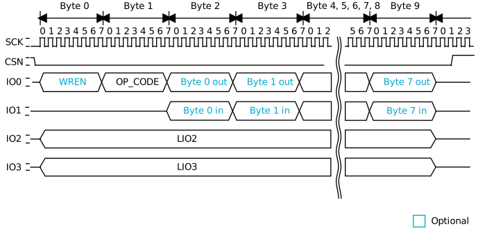
Long frame mode
The LFEN and LFSTOP fields in the CINSTRCONF register control the operation of the custom instruction Long frame mode. Long frame mode is a mechanism that permits arbitrary byte length custom instructions. While in Long frame mode a long custom instruction sequence is split in multiple writes to the CINSTRDAT0 and CINSTRDAT1 registers.
To enable Long frame mode every write to the CINSTRCONF register must have the LFEN field set to 1. The contents
of the OPCODE field will be transmitted after the first write to CINSTRCONF and will be omitted in every subsequent write to
this register. For subsequent writes the number of data bytes as specified in the LENGTH field
are transferred (that is the value of LENGTH - 1 data bytes). The values of the LIO2 and LIO3 fields are
set in the first write to CINSTRCONF and will apply for
the entire custom instruction transmission until the long frame is finalized.
To finalize a long frame transmission, the LFSTOP field in the CINSTRCONF register must be set to 1 in the last write to this
register.
Deep power-down mode
The external flash memory can be put in Deep power-down mode (DPM) to minimize its current consumption when there is no need to access the memory.
DPM is enabled in register IFCONFIG0 and configured in register DPMDUR. The DPM status of the external memory can be read in the STATUS register. The DPMDUR register has to be configured according to the external flash specification to get the information in the STATUS register and the timing of the READY event correct.
Entering or exiting DPM is controlled using register IFCONFIG1.
Instruction set
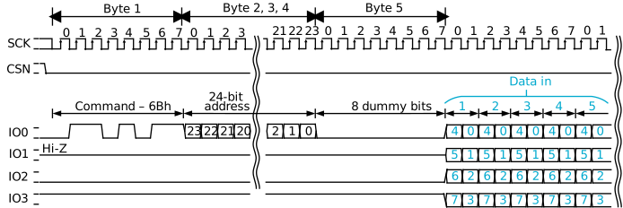
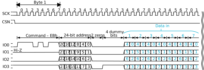
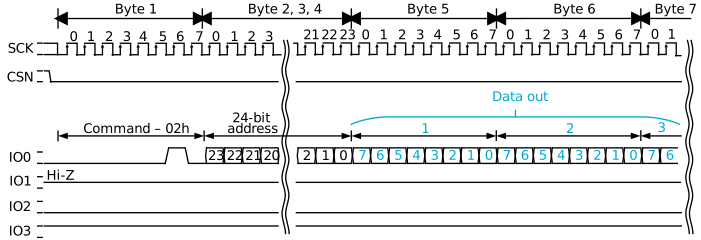
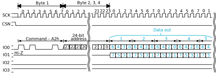
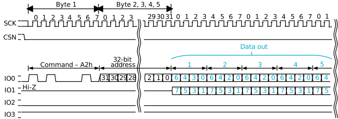
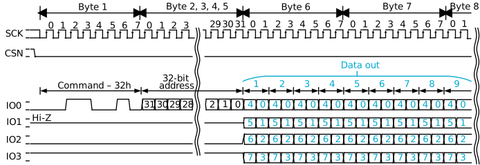
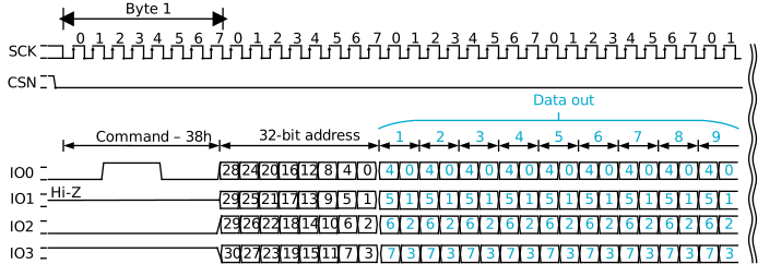
The following table shows the instruction set supported by QSPI when communicating with an external flash device.
| Instruction | Opcode | Description |
|---|---|---|
| WREN | 0x06 | Write enable |
| RDSR | 0x05 | Read status register |
| WRSR | 0x01 | Write status register |
| FASTREAD | 0x0B | Read bytes at higher speed |
| READ2O | 0x3B | Dual-read output |
| READ2IO | 0xBB | Dual-read input/output |
| READ4O | 0x6B | Quad-read output |
| READ4IO | 0xEB | Quad-read input/output |
| PP | 0x02 | Page program |
| PP2O | 0xA2 | Dual-page program output |
| PP4O | 0x32 | Quad-page program output |
| PP4IO | 0x38 | Quad-page program input/output |
| SE | 0x20 | Sector erase |
| BE | 0xD8 | Block erase |
| CE | 0xC7 | Chip erase |
| DP | 0xB9 | Enter Deep power-down mode |
| DPE | 0xAB | Exit Deep power-down mode |
| EN4B | Specified in the ADDRCONF register | Enable 32 bit address mode |
Interface description
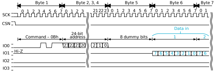
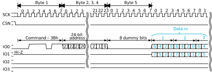
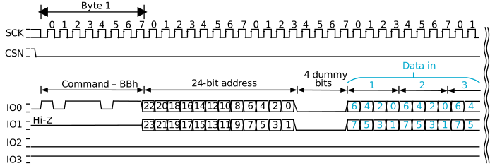
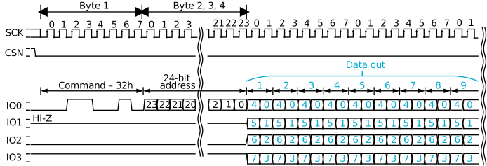
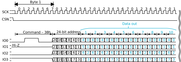
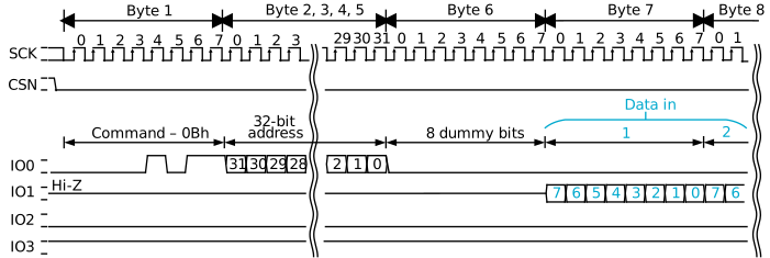
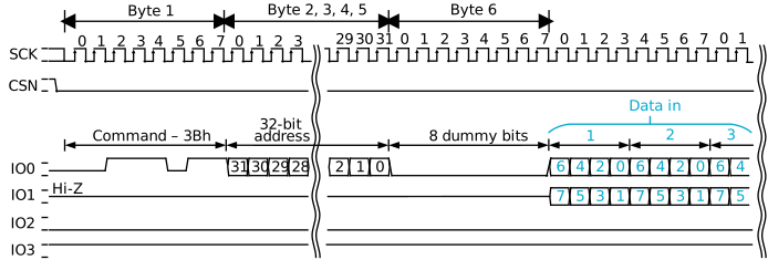
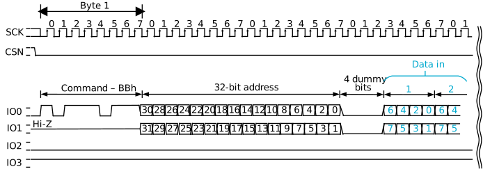
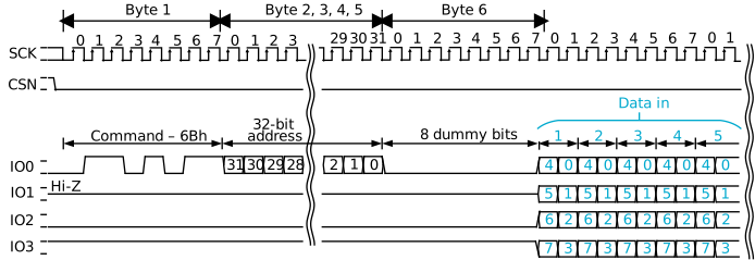
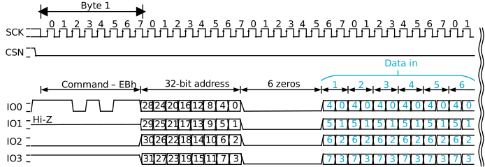
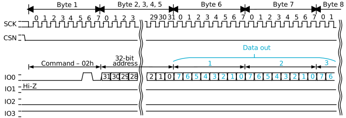
Registers
Instances
| Instance | Domain | Base address | TrustZone | Split access | Description | ||
|---|---|---|---|---|---|---|---|
| Map | Att | DMA | |||||
QSPI : S | APPLICATION | 0x5002B000 | US | S | SA | No | External memory (quad serial peripheral) interface |
Configuration
| Instance | Domain | Configuration |
|---|---|---|
QSPI : S | APPLICATION | Supports 192 MHz and 96 MHz PCLK192M frequency |
Register overview
| Register | Offset | TZ | Description |
|---|---|---|---|
| TASKS_ACTIVATE | 0x000 | Activate QSPI interface | |
| TASKS_READSTART | 0x004 | Start transfer from external flash memory to internal RAM | |
| TASKS_WRITESTART | 0x008 | Start transfer from internal RAM to external flash memory | |
| TASKS_ERASESTART | 0x00C | Start external flash memory erase operation | |
| TASKS_DEACTIVATE | 0x010 | Deactivate QSPI interface | |
| SUBSCRIBE_ACTIVATE | 0x080 | Subscribe configuration for task ACTIVATE | |
| SUBSCRIBE_READSTART | 0x084 | Subscribe configuration for task READSTART | |
| SUBSCRIBE_WRITESTART | 0x088 | Subscribe configuration for task WRITESTART | |
| SUBSCRIBE_ERASESTART | 0x08C | Subscribe configuration for task ERASESTART | |
| SUBSCRIBE_DEACTIVATE | 0x090 | Subscribe configuration for task DEACTIVATE | |
| EVENTS_READY | 0x100 | QSPI peripheral is ready. This event will be generated as a response to all QSPI tasks except DEACTIVATE. | |
| PUBLISH_READY | 0x180 | Publish configuration for event READY | |
| INTEN | 0x300 | Enable or disable interrupt | |
| INTENSET | 0x304 | Enable interrupt | |
| INTENCLR | 0x308 | Disable interrupt | |
| ENABLE | 0x500 | Enable QSPI peripheral and acquire the pins selected in PSELn registers | |
| READ.SRC | 0x504 | Flash memory source address | |
| READ.DST | 0x508 | RAM destination address | |
| READ.CNT | 0x50C | Read transfer length | |
| WRITE.DST | 0x510 | Flash destination address | |
| WRITE.SRC | 0x514 | RAM source address | |
| WRITE.CNT | 0x518 | Write transfer length | |
| ERASE.PTR | 0x51C | Start address of flash block to be erased | |
| ERASE.LEN | 0x520 | Size of block to be erased. | |
| PSEL.SCK | 0x524 | Pin select for serial clock SCK | |
| PSEL.CSN | 0x528 | Pin select for chip select signal CSN. | |
| PSEL.IO0 | 0x530 | Pin select for serial data MOSI/IO0. | |
| PSEL.IO1 | 0x534 | Pin select for serial data MISO/IO1. | |
| PSEL.IO2 | 0x538 | Pin select for serial data WP/IO2. | |
| PSEL.IO3 | 0x53C | Pin select for serial data HOLD/IO3. | |
| XIPOFFSET | 0x540 | Address offset into the external memory for Execute in Place operation. | |
| IFCONFIG0 | 0x544 | Interface configuration. | |
| XIPEN | 0x54C | Enable Execute in Place operation. | |
| XIP_ENC.KEY0 | 0x560 | Bits 31:0 of XIP AES KEY | |
| XIP_ENC.KEY1 | 0x564 | Bits 63:32 of XIP AES KEY | |
| XIP_ENC.KEY2 | 0x568 | Bits 95:64 of XIP AES KEY | |
| XIP_ENC.KEY3 | 0x56C | Bits 127:96 of XIP AES KEY | |
| XIP_ENC.NONCE0 | 0x570 | Bits 31:0 of XIP NONCE | |
| XIP_ENC.NONCE1 | 0x574 | Bits 63:32 of XIP NONCE | |
| XIP_ENC.NONCE2 | 0x578 | Bits 95:64 of XIP NONCE | |
| XIP_ENC.ENABLE | 0x57C | Enable stream cipher for XIP | |
| DMA_ENC.KEY0 | 0x580 | Bits 31:0 of DMA AES KEY | |
| DMA_ENC.KEY1 | 0x584 | Bits 63:32 of DMA AES KEY | |
| DMA_ENC.KEY2 | 0x588 | Bits 95:64 of DMA AES KEY | |
| DMA_ENC.KEY3 | 0x58C | Bits 127:96 of DMA AES KEY | |
| DMA_ENC.NONCE0 | 0x590 | Bits 31:0 of DMA NONCE | |
| DMA_ENC.NONCE1 | 0x594 | Bits 63:32 of DMA NONCE | |
| DMA_ENC.NONCE2 | 0x598 | Bits 95:64 of DMA NONCE | |
| DMA_ENC.ENABLE | 0x59C | Enable stream cipher for EasyDMA | |
| IFCONFIG1 | 0x600 | Interface configuration. | |
| STATUS | 0x604 | Status register. | |
| DPMDUR | 0x614 | Set the duration required to enter/exit deep power-down mode (DPM). | |
| ADDRCONF | 0x624 | Extended address configuration. | |
| CINSTRCONF | 0x634 | Custom instruction configuration register. | |
| CINSTRDAT0 | 0x638 | Custom instruction data register 0. | |
| CINSTRDAT1 | 0x63C | Custom instruction data register 1. | |
| IFTIMING | 0x640 | SPI interface timing. |
TASKS_ACTIVATE
Address offset: 0x000
Activate QSPI interface
Triggering this task activates the external flash memory interface and initiates communication with the external memory. The READY event is generated when the activation has been completed.
| Bit number | 31 | 30 | 29 | 28 | 27 | 26 | 25 | 24 | 23 | 22 | 21 | 20 | 19 | 18 | 17 | 16 | 15 | 14 | 13 | 12 | 11 | 10 | 9 | 8 | 7 | 6 | 5 | 4 | 3 | 2 | 1 | 0 | |||
|---|---|---|---|---|---|---|---|---|---|---|---|---|---|---|---|---|---|---|---|---|---|---|---|---|---|---|---|---|---|---|---|---|---|---|---|
| ID | A | ||||||||||||||||||||||||||||||||||
| Reset 0x00000000 | 0 | 0 | 0 | 0 | 0 | 0 | 0 | 0 | 0 | 0 | 0 | 0 | 0 | 0 | 0 | 0 | 0 | 0 | 0 | 0 | 0 | 0 | 0 | 0 | 0 | 0 | 0 | 0 | 0 | 0 | 0 | 0 | |||
| ID | R/W | Field | Value ID | Value | Description | ||||||||||||||||||||||||||||||
| A | W | TASKS_ACTIVATE | Activate QSPI interface Triggering this task activates the external flash memory interface and initiates communication with the external memory. The READY event is generated when the activation has been completed. | ||||||||||||||||||||||||||||||||
Trigger | 1 | Trigger task | |||||||||||||||||||||||||||||||||
TASKS_READSTART
Address offset: 0x004
Start transfer from external flash memory to internal RAM
The READY event will be generated when transfer is complete.
| Bit number | 31 | 30 | 29 | 28 | 27 | 26 | 25 | 24 | 23 | 22 | 21 | 20 | 19 | 18 | 17 | 16 | 15 | 14 | 13 | 12 | 11 | 10 | 9 | 8 | 7 | 6 | 5 | 4 | 3 | 2 | 1 | 0 | |||
|---|---|---|---|---|---|---|---|---|---|---|---|---|---|---|---|---|---|---|---|---|---|---|---|---|---|---|---|---|---|---|---|---|---|---|---|
| ID | A | ||||||||||||||||||||||||||||||||||
| Reset 0x00000000 | 0 | 0 | 0 | 0 | 0 | 0 | 0 | 0 | 0 | 0 | 0 | 0 | 0 | 0 | 0 | 0 | 0 | 0 | 0 | 0 | 0 | 0 | 0 | 0 | 0 | 0 | 0 | 0 | 0 | 0 | 0 | 0 | |||
| ID | R/W | Field | Value ID | Value | Description | ||||||||||||||||||||||||||||||
| A | W | TASKS_READSTART | Start transfer from external flash memory to internal RAM The READY event will be generated when transfer is complete. | ||||||||||||||||||||||||||||||||
Trigger | 1 | Trigger task | |||||||||||||||||||||||||||||||||
TASKS_WRITESTART
Address offset: 0x008
Start transfer from internal RAM to external flash memory
The READY event will be generated when transfer is complete.
| Bit number | 31 | 30 | 29 | 28 | 27 | 26 | 25 | 24 | 23 | 22 | 21 | 20 | 19 | 18 | 17 | 16 | 15 | 14 | 13 | 12 | 11 | 10 | 9 | 8 | 7 | 6 | 5 | 4 | 3 | 2 | 1 | 0 | |||
|---|---|---|---|---|---|---|---|---|---|---|---|---|---|---|---|---|---|---|---|---|---|---|---|---|---|---|---|---|---|---|---|---|---|---|---|
| ID | A | ||||||||||||||||||||||||||||||||||
| Reset 0x00000000 | 0 | 0 | 0 | 0 | 0 | 0 | 0 | 0 | 0 | 0 | 0 | 0 | 0 | 0 | 0 | 0 | 0 | 0 | 0 | 0 | 0 | 0 | 0 | 0 | 0 | 0 | 0 | 0 | 0 | 0 | 0 | 0 | |||
| ID | R/W | Field | Value ID | Value | Description | ||||||||||||||||||||||||||||||
| A | W | TASKS_WRITESTART | Start transfer from internal RAM to external flash memory The READY event will be generated when transfer is complete. | ||||||||||||||||||||||||||||||||
Trigger | 1 | Trigger task | |||||||||||||||||||||||||||||||||
TASKS_ERASESTART
Address offset: 0x00C
Start external flash memory erase operation
The READY event will be generated when the erase operation has been started. The generation of the READY event does not imply that the erase operation is completed.
| Bit number | 31 | 30 | 29 | 28 | 27 | 26 | 25 | 24 | 23 | 22 | 21 | 20 | 19 | 18 | 17 | 16 | 15 | 14 | 13 | 12 | 11 | 10 | 9 | 8 | 7 | 6 | 5 | 4 | 3 | 2 | 1 | 0 | |||
|---|---|---|---|---|---|---|---|---|---|---|---|---|---|---|---|---|---|---|---|---|---|---|---|---|---|---|---|---|---|---|---|---|---|---|---|
| ID | A | ||||||||||||||||||||||||||||||||||
| Reset 0x00000000 | 0 | 0 | 0 | 0 | 0 | 0 | 0 | 0 | 0 | 0 | 0 | 0 | 0 | 0 | 0 | 0 | 0 | 0 | 0 | 0 | 0 | 0 | 0 | 0 | 0 | 0 | 0 | 0 | 0 | 0 | 0 | 0 | |||
| ID | R/W | Field | Value ID | Value | Description | ||||||||||||||||||||||||||||||
| A | W | TASKS_ERASESTART | Start external flash memory erase operation The READY event will be generated when the erase operation has been started. The generation of the READY event does not imply that the erase operation is completed. | ||||||||||||||||||||||||||||||||
Trigger | 1 | Trigger task | |||||||||||||||||||||||||||||||||
TASKS_DEACTIVATE
Address offset: 0x010
Deactivate QSPI interface
This task might be needed to optimize current consumption in case there are any added current consumption when QSPI interface is activated, but idle.
| Bit number | 31 | 30 | 29 | 28 | 27 | 26 | 25 | 24 | 23 | 22 | 21 | 20 | 19 | 18 | 17 | 16 | 15 | 14 | 13 | 12 | 11 | 10 | 9 | 8 | 7 | 6 | 5 | 4 | 3 | 2 | 1 | 0 | |||
|---|---|---|---|---|---|---|---|---|---|---|---|---|---|---|---|---|---|---|---|---|---|---|---|---|---|---|---|---|---|---|---|---|---|---|---|
| ID | A | ||||||||||||||||||||||||||||||||||
| Reset 0x00000000 | 0 | 0 | 0 | 0 | 0 | 0 | 0 | 0 | 0 | 0 | 0 | 0 | 0 | 0 | 0 | 0 | 0 | 0 | 0 | 0 | 0 | 0 | 0 | 0 | 0 | 0 | 0 | 0 | 0 | 0 | 0 | 0 | |||
| ID | R/W | Field | Value ID | Value | Description | ||||||||||||||||||||||||||||||
| A | W | TASKS_DEACTIVATE | Deactivate QSPI interface This task might be needed to optimize current consumption in case there are any added current consumption when QSPI interface is activated, but idle. | ||||||||||||||||||||||||||||||||
Trigger | 1 | Trigger task | |||||||||||||||||||||||||||||||||
SUBSCRIBE_ACTIVATE
Address offset: 0x080
Subscribe configuration for task ACTIVATE
Triggering this task activates the external flash memory interface and initiates communication with the external memory. The READY event is generated when the activation has been completed.
| Bit number | 31 | 30 | 29 | 28 | 27 | 26 | 25 | 24 | 23 | 22 | 21 | 20 | 19 | 18 | 17 | 16 | 15 | 14 | 13 | 12 | 11 | 10 | 9 | 8 | 7 | 6 | 5 | 4 | 3 | 2 | 1 | 0 | |||
|---|---|---|---|---|---|---|---|---|---|---|---|---|---|---|---|---|---|---|---|---|---|---|---|---|---|---|---|---|---|---|---|---|---|---|---|
| ID | B | A | A | A | A | A | A | A | A | ||||||||||||||||||||||||||
| Reset 0x00000000 | 0 | 0 | 0 | 0 | 0 | 0 | 0 | 0 | 0 | 0 | 0 | 0 | 0 | 0 | 0 | 0 | 0 | 0 | 0 | 0 | 0 | 0 | 0 | 0 | 0 | 0 | 0 | 0 | 0 | 0 | 0 | 0 | |||
| ID | R/W | Field | Value ID | Value | Description | ||||||||||||||||||||||||||||||
| A | RW | CHIDX | [0..255] | DPPI channel that task ACTIVATE will subscribe to | |||||||||||||||||||||||||||||||
| B | RW | EN | |||||||||||||||||||||||||||||||||
Disabled | 0 | Disable subscription | |||||||||||||||||||||||||||||||||
Enabled | 1 | Enable subscription | |||||||||||||||||||||||||||||||||
SUBSCRIBE_READSTART
Address offset: 0x084
Subscribe configuration for task READSTART
The READY event will be generated when transfer is complete.
| Bit number | 31 | 30 | 29 | 28 | 27 | 26 | 25 | 24 | 23 | 22 | 21 | 20 | 19 | 18 | 17 | 16 | 15 | 14 | 13 | 12 | 11 | 10 | 9 | 8 | 7 | 6 | 5 | 4 | 3 | 2 | 1 | 0 | |||
|---|---|---|---|---|---|---|---|---|---|---|---|---|---|---|---|---|---|---|---|---|---|---|---|---|---|---|---|---|---|---|---|---|---|---|---|
| ID | B | A | A | A | A | A | A | A | A | ||||||||||||||||||||||||||
| Reset 0x00000000 | 0 | 0 | 0 | 0 | 0 | 0 | 0 | 0 | 0 | 0 | 0 | 0 | 0 | 0 | 0 | 0 | 0 | 0 | 0 | 0 | 0 | 0 | 0 | 0 | 0 | 0 | 0 | 0 | 0 | 0 | 0 | 0 | |||
| ID | R/W | Field | Value ID | Value | Description | ||||||||||||||||||||||||||||||
| A | RW | CHIDX | [0..255] | DPPI channel that task READSTART will subscribe to | |||||||||||||||||||||||||||||||
| B | RW | EN | |||||||||||||||||||||||||||||||||
Disabled | 0 | Disable subscription | |||||||||||||||||||||||||||||||||
Enabled | 1 | Enable subscription | |||||||||||||||||||||||||||||||||
SUBSCRIBE_WRITESTART
Address offset: 0x088
Subscribe configuration for task WRITESTART
The READY event will be generated when transfer is complete.
| Bit number | 31 | 30 | 29 | 28 | 27 | 26 | 25 | 24 | 23 | 22 | 21 | 20 | 19 | 18 | 17 | 16 | 15 | 14 | 13 | 12 | 11 | 10 | 9 | 8 | 7 | 6 | 5 | 4 | 3 | 2 | 1 | 0 | |||
|---|---|---|---|---|---|---|---|---|---|---|---|---|---|---|---|---|---|---|---|---|---|---|---|---|---|---|---|---|---|---|---|---|---|---|---|
| ID | B | A | A | A | A | A | A | A | A | ||||||||||||||||||||||||||
| Reset 0x00000000 | 0 | 0 | 0 | 0 | 0 | 0 | 0 | 0 | 0 | 0 | 0 | 0 | 0 | 0 | 0 | 0 | 0 | 0 | 0 | 0 | 0 | 0 | 0 | 0 | 0 | 0 | 0 | 0 | 0 | 0 | 0 | 0 | |||
| ID | R/W | Field | Value ID | Value | Description | ||||||||||||||||||||||||||||||
| A | RW | CHIDX | [0..255] | DPPI channel that task WRITESTART will subscribe to | |||||||||||||||||||||||||||||||
| B | RW | EN | |||||||||||||||||||||||||||||||||
Disabled | 0 | Disable subscription | |||||||||||||||||||||||||||||||||
Enabled | 1 | Enable subscription | |||||||||||||||||||||||||||||||||
SUBSCRIBE_ERASESTART
Address offset: 0x08C
Subscribe configuration for task ERASESTART
The READY event will be generated when the erase operation has been started. The generation of the READY event does not imply that the erase operation is completed.
| Bit number | 31 | 30 | 29 | 28 | 27 | 26 | 25 | 24 | 23 | 22 | 21 | 20 | 19 | 18 | 17 | 16 | 15 | 14 | 13 | 12 | 11 | 10 | 9 | 8 | 7 | 6 | 5 | 4 | 3 | 2 | 1 | 0 | |||
|---|---|---|---|---|---|---|---|---|---|---|---|---|---|---|---|---|---|---|---|---|---|---|---|---|---|---|---|---|---|---|---|---|---|---|---|
| ID | B | A | A | A | A | A | A | A | A | ||||||||||||||||||||||||||
| Reset 0x00000000 | 0 | 0 | 0 | 0 | 0 | 0 | 0 | 0 | 0 | 0 | 0 | 0 | 0 | 0 | 0 | 0 | 0 | 0 | 0 | 0 | 0 | 0 | 0 | 0 | 0 | 0 | 0 | 0 | 0 | 0 | 0 | 0 | |||
| ID | R/W | Field | Value ID | Value | Description | ||||||||||||||||||||||||||||||
| A | RW | CHIDX | [0..255] | DPPI channel that task ERASESTART will subscribe to | |||||||||||||||||||||||||||||||
| B | RW | EN | |||||||||||||||||||||||||||||||||
Disabled | 0 | Disable subscription | |||||||||||||||||||||||||||||||||
Enabled | 1 | Enable subscription | |||||||||||||||||||||||||||||||||
SUBSCRIBE_DEACTIVATE
Address offset: 0x090
Subscribe configuration for task DEACTIVATE
This task might be needed to optimize current consumption in case there are any added current consumption when QSPI interface is activated, but idle.
| Bit number | 31 | 30 | 29 | 28 | 27 | 26 | 25 | 24 | 23 | 22 | 21 | 20 | 19 | 18 | 17 | 16 | 15 | 14 | 13 | 12 | 11 | 10 | 9 | 8 | 7 | 6 | 5 | 4 | 3 | 2 | 1 | 0 | |||
|---|---|---|---|---|---|---|---|---|---|---|---|---|---|---|---|---|---|---|---|---|---|---|---|---|---|---|---|---|---|---|---|---|---|---|---|
| ID | B | A | A | A | A | A | A | A | A | ||||||||||||||||||||||||||
| Reset 0x00000000 | 0 | 0 | 0 | 0 | 0 | 0 | 0 | 0 | 0 | 0 | 0 | 0 | 0 | 0 | 0 | 0 | 0 | 0 | 0 | 0 | 0 | 0 | 0 | 0 | 0 | 0 | 0 | 0 | 0 | 0 | 0 | 0 | |||
| ID | R/W | Field | Value ID | Value | Description | ||||||||||||||||||||||||||||||
| A | RW | CHIDX | [0..255] | DPPI channel that task DEACTIVATE will subscribe to | |||||||||||||||||||||||||||||||
| B | RW | EN | |||||||||||||||||||||||||||||||||
Disabled | 0 | Disable subscription | |||||||||||||||||||||||||||||||||
Enabled | 1 | Enable subscription | |||||||||||||||||||||||||||||||||
EVENTS_READY
Address offset: 0x100
QSPI peripheral is ready. This event will be generated as a response to all QSPI tasks except DEACTIVATE.
| Bit number | 31 | 30 | 29 | 28 | 27 | 26 | 25 | 24 | 23 | 22 | 21 | 20 | 19 | 18 | 17 | 16 | 15 | 14 | 13 | 12 | 11 | 10 | 9 | 8 | 7 | 6 | 5 | 4 | 3 | 2 | 1 | 0 | |||
|---|---|---|---|---|---|---|---|---|---|---|---|---|---|---|---|---|---|---|---|---|---|---|---|---|---|---|---|---|---|---|---|---|---|---|---|
| ID | A | ||||||||||||||||||||||||||||||||||
| Reset 0x00000000 | 0 | 0 | 0 | 0 | 0 | 0 | 0 | 0 | 0 | 0 | 0 | 0 | 0 | 0 | 0 | 0 | 0 | 0 | 0 | 0 | 0 | 0 | 0 | 0 | 0 | 0 | 0 | 0 | 0 | 0 | 0 | 0 | |||
| ID | R/W | Field | Value ID | Value | Description | ||||||||||||||||||||||||||||||
| A | RW | EVENTS_READY | QSPI peripheral is ready. This event will be generated as a response to all QSPI tasks except DEACTIVATE. | ||||||||||||||||||||||||||||||||
NotGenerated | 0 | Event not generated | |||||||||||||||||||||||||||||||||
Generated | 1 | Event generated | |||||||||||||||||||||||||||||||||
PUBLISH_READY
Address offset: 0x180
Publish configuration for event READY
| Bit number | 31 | 30 | 29 | 28 | 27 | 26 | 25 | 24 | 23 | 22 | 21 | 20 | 19 | 18 | 17 | 16 | 15 | 14 | 13 | 12 | 11 | 10 | 9 | 8 | 7 | 6 | 5 | 4 | 3 | 2 | 1 | 0 | |||
|---|---|---|---|---|---|---|---|---|---|---|---|---|---|---|---|---|---|---|---|---|---|---|---|---|---|---|---|---|---|---|---|---|---|---|---|
| ID | B | A | A | A | A | A | A | A | A | ||||||||||||||||||||||||||
| Reset 0x00000000 | 0 | 0 | 0 | 0 | 0 | 0 | 0 | 0 | 0 | 0 | 0 | 0 | 0 | 0 | 0 | 0 | 0 | 0 | 0 | 0 | 0 | 0 | 0 | 0 | 0 | 0 | 0 | 0 | 0 | 0 | 0 | 0 | |||
| ID | R/W | Field | Value ID | Value | Description | ||||||||||||||||||||||||||||||
| A | RW | CHIDX | [0..255] | DPPI channel that event READY will publish to | |||||||||||||||||||||||||||||||
| B | RW | EN | |||||||||||||||||||||||||||||||||
Disabled | 0 | Disable publishing | |||||||||||||||||||||||||||||||||
Enabled | 1 | Enable publishing | |||||||||||||||||||||||||||||||||
INTEN
Address offset: 0x300
Enable or disable interrupt
| Bit number | 31 | 30 | 29 | 28 | 27 | 26 | 25 | 24 | 23 | 22 | 21 | 20 | 19 | 18 | 17 | 16 | 15 | 14 | 13 | 12 | 11 | 10 | 9 | 8 | 7 | 6 | 5 | 4 | 3 | 2 | 1 | 0 | |||
|---|---|---|---|---|---|---|---|---|---|---|---|---|---|---|---|---|---|---|---|---|---|---|---|---|---|---|---|---|---|---|---|---|---|---|---|
| ID | A | ||||||||||||||||||||||||||||||||||
| Reset 0x00000000 | 0 | 0 | 0 | 0 | 0 | 0 | 0 | 0 | 0 | 0 | 0 | 0 | 0 | 0 | 0 | 0 | 0 | 0 | 0 | 0 | 0 | 0 | 0 | 0 | 0 | 0 | 0 | 0 | 0 | 0 | 0 | 0 | |||
| ID | R/W | Field | Value ID | Value | Description | ||||||||||||||||||||||||||||||
| A | RW | READY | Enable or disable interrupt for event READY | ||||||||||||||||||||||||||||||||
Disabled | 0 | Disable | |||||||||||||||||||||||||||||||||
Enabled | 1 | Enable | |||||||||||||||||||||||||||||||||
INTENSET
Address offset: 0x304
Enable interrupt
| Bit number | 31 | 30 | 29 | 28 | 27 | 26 | 25 | 24 | 23 | 22 | 21 | 20 | 19 | 18 | 17 | 16 | 15 | 14 | 13 | 12 | 11 | 10 | 9 | 8 | 7 | 6 | 5 | 4 | 3 | 2 | 1 | 0 | |||
|---|---|---|---|---|---|---|---|---|---|---|---|---|---|---|---|---|---|---|---|---|---|---|---|---|---|---|---|---|---|---|---|---|---|---|---|
| ID | A | ||||||||||||||||||||||||||||||||||
| Reset 0x00000000 | 0 | 0 | 0 | 0 | 0 | 0 | 0 | 0 | 0 | 0 | 0 | 0 | 0 | 0 | 0 | 0 | 0 | 0 | 0 | 0 | 0 | 0 | 0 | 0 | 0 | 0 | 0 | 0 | 0 | 0 | 0 | 0 | |||
| ID | R/W | Field | Value ID | Value | Description | ||||||||||||||||||||||||||||||
| A | RW | READY | Write '1' to enable interrupt for event READY | ||||||||||||||||||||||||||||||||
Set | 1 | Enable | |||||||||||||||||||||||||||||||||
Disabled | 0 | Read: Disabled | |||||||||||||||||||||||||||||||||
Enabled | 1 | Read: Enabled | |||||||||||||||||||||||||||||||||
INTENCLR
Address offset: 0x308
Disable interrupt
| Bit number | 31 | 30 | 29 | 28 | 27 | 26 | 25 | 24 | 23 | 22 | 21 | 20 | 19 | 18 | 17 | 16 | 15 | 14 | 13 | 12 | 11 | 10 | 9 | 8 | 7 | 6 | 5 | 4 | 3 | 2 | 1 | 0 | |||
|---|---|---|---|---|---|---|---|---|---|---|---|---|---|---|---|---|---|---|---|---|---|---|---|---|---|---|---|---|---|---|---|---|---|---|---|
| ID | A | ||||||||||||||||||||||||||||||||||
| Reset 0x00000000 | 0 | 0 | 0 | 0 | 0 | 0 | 0 | 0 | 0 | 0 | 0 | 0 | 0 | 0 | 0 | 0 | 0 | 0 | 0 | 0 | 0 | 0 | 0 | 0 | 0 | 0 | 0 | 0 | 0 | 0 | 0 | 0 | |||
| ID | R/W | Field | Value ID | Value | Description | ||||||||||||||||||||||||||||||
| A | RW | READY | Write '1' to disable interrupt for event READY | ||||||||||||||||||||||||||||||||
Clear | 1 | Disable | |||||||||||||||||||||||||||||||||
Disabled | 0 | Read: Disabled | |||||||||||||||||||||||||||||||||
Enabled | 1 | Read: Enabled | |||||||||||||||||||||||||||||||||
ENABLE
Address offset: 0x500
Enable QSPI peripheral and acquire the pins selected in PSELn registers
| Bit number | 31 | 30 | 29 | 28 | 27 | 26 | 25 | 24 | 23 | 22 | 21 | 20 | 19 | 18 | 17 | 16 | 15 | 14 | 13 | 12 | 11 | 10 | 9 | 8 | 7 | 6 | 5 | 4 | 3 | 2 | 1 | 0 | |||
|---|---|---|---|---|---|---|---|---|---|---|---|---|---|---|---|---|---|---|---|---|---|---|---|---|---|---|---|---|---|---|---|---|---|---|---|
| ID | A | ||||||||||||||||||||||||||||||||||
| Reset 0x00000000 | 0 | 0 | 0 | 0 | 0 | 0 | 0 | 0 | 0 | 0 | 0 | 0 | 0 | 0 | 0 | 0 | 0 | 0 | 0 | 0 | 0 | 0 | 0 | 0 | 0 | 0 | 0 | 0 | 0 | 0 | 0 | 0 | |||
| ID | R/W | Field | Value ID | Value | Description | ||||||||||||||||||||||||||||||
| A | RW | ENABLE | Enable or disable QSPI | ||||||||||||||||||||||||||||||||
Disabled | 0 | Disable QSPI | |||||||||||||||||||||||||||||||||
Enabled | 1 | Enable QSPI | |||||||||||||||||||||||||||||||||
READ.SRC
Address offset: 0x504
Flash memory source address
| Bit number | 31 | 30 | 29 | 28 | 27 | 26 | 25 | 24 | 23 | 22 | 21 | 20 | 19 | 18 | 17 | 16 | 15 | 14 | 13 | 12 | 11 | 10 | 9 | 8 | 7 | 6 | 5 | 4 | 3 | 2 | 1 | 0 | |||
|---|---|---|---|---|---|---|---|---|---|---|---|---|---|---|---|---|---|---|---|---|---|---|---|---|---|---|---|---|---|---|---|---|---|---|---|
| ID | A | A | A | A | A | A | A | A | A | A | A | A | A | A | A | A | A | A | A | A | A | A | A | A | A | A | A | A | A | A | A | A | |||
| Reset 0x00000000 | 0 | 0 | 0 | 0 | 0 | 0 | 0 | 0 | 0 | 0 | 0 | 0 | 0 | 0 | 0 | 0 | 0 | 0 | 0 | 0 | 0 | 0 | 0 | 0 | 0 | 0 | 0 | 0 | 0 | 0 | 0 | 0 | |||
| ID | R/W | Field | Value ID | Value | Description | ||||||||||||||||||||||||||||||
| A | RW | SRC | Word-aligned flash memory source address. | ||||||||||||||||||||||||||||||||
READ.DST
Address offset: 0x508
RAM destination address
| Bit number | 31 | 30 | 29 | 28 | 27 | 26 | 25 | 24 | 23 | 22 | 21 | 20 | 19 | 18 | 17 | 16 | 15 | 14 | 13 | 12 | 11 | 10 | 9 | 8 | 7 | 6 | 5 | 4 | 3 | 2 | 1 | 0 | |||
|---|---|---|---|---|---|---|---|---|---|---|---|---|---|---|---|---|---|---|---|---|---|---|---|---|---|---|---|---|---|---|---|---|---|---|---|
| ID | A | A | A | A | A | A | A | A | A | A | A | A | A | A | A | A | A | A | A | A | A | A | A | A | A | A | A | A | A | A | A | A | |||
| Reset 0x00000000 | 0 | 0 | 0 | 0 | 0 | 0 | 0 | 0 | 0 | 0 | 0 | 0 | 0 | 0 | 0 | 0 | 0 | 0 | 0 | 0 | 0 | 0 | 0 | 0 | 0 | 0 | 0 | 0 | 0 | 0 | 0 | 0 | |||
| ID | R/W | Field | Value ID | Value | Description | ||||||||||||||||||||||||||||||
| A | RW | DST | Word-aligned RAM destination address. | ||||||||||||||||||||||||||||||||
READ.CNT
Address offset: 0x50C
Read transfer length
| Bit number | 31 | 30 | 29 | 28 | 27 | 26 | 25 | 24 | 23 | 22 | 21 | 20 | 19 | 18 | 17 | 16 | 15 | 14 | 13 | 12 | 11 | 10 | 9 | 8 | 7 | 6 | 5 | 4 | 3 | 2 | 1 | 0 | |||
|---|---|---|---|---|---|---|---|---|---|---|---|---|---|---|---|---|---|---|---|---|---|---|---|---|---|---|---|---|---|---|---|---|---|---|---|
| ID | A | A | A | A | A | A | A | A | A | A | A | A | A | A | A | A | A | A | A | A | A | ||||||||||||||
| Reset 0x00000000 | 0 | 0 | 0 | 0 | 0 | 0 | 0 | 0 | 0 | 0 | 0 | 0 | 0 | 0 | 0 | 0 | 0 | 0 | 0 | 0 | 0 | 0 | 0 | 0 | 0 | 0 | 0 | 0 | 0 | 0 | 0 | 0 | |||
| ID | R/W | Field | Value ID | Value | Description | ||||||||||||||||||||||||||||||
| A | RW | CNT | Read transfer length in number of bytes. The length must be a multiple of 4 bytes. | ||||||||||||||||||||||||||||||||
WRITE.DST
Address offset: 0x510
Flash destination address
| Bit number | 31 | 30 | 29 | 28 | 27 | 26 | 25 | 24 | 23 | 22 | 21 | 20 | 19 | 18 | 17 | 16 | 15 | 14 | 13 | 12 | 11 | 10 | 9 | 8 | 7 | 6 | 5 | 4 | 3 | 2 | 1 | 0 | |||
|---|---|---|---|---|---|---|---|---|---|---|---|---|---|---|---|---|---|---|---|---|---|---|---|---|---|---|---|---|---|---|---|---|---|---|---|
| ID | A | A | A | A | A | A | A | A | A | A | A | A | A | A | A | A | A | A | A | A | A | A | A | A | A | A | A | A | A | A | A | A | |||
| Reset 0x00000000 | 0 | 0 | 0 | 0 | 0 | 0 | 0 | 0 | 0 | 0 | 0 | 0 | 0 | 0 | 0 | 0 | 0 | 0 | 0 | 0 | 0 | 0 | 0 | 0 | 0 | 0 | 0 | 0 | 0 | 0 | 0 | 0 | |||
| ID | R/W | Field | Value ID | Value | Description | ||||||||||||||||||||||||||||||
| A | RW | DST | Word-aligned flash destination address. | ||||||||||||||||||||||||||||||||
WRITE.SRC
Address offset: 0x514
RAM source address
| Bit number | 31 | 30 | 29 | 28 | 27 | 26 | 25 | 24 | 23 | 22 | 21 | 20 | 19 | 18 | 17 | 16 | 15 | 14 | 13 | 12 | 11 | 10 | 9 | 8 | 7 | 6 | 5 | 4 | 3 | 2 | 1 | 0 | |||
|---|---|---|---|---|---|---|---|---|---|---|---|---|---|---|---|---|---|---|---|---|---|---|---|---|---|---|---|---|---|---|---|---|---|---|---|
| ID | A | A | A | A | A | A | A | A | A | A | A | A | A | A | A | A | A | A | A | A | A | A | A | A | A | A | A | A | A | A | A | A | |||
| Reset 0x00000000 | 0 | 0 | 0 | 0 | 0 | 0 | 0 | 0 | 0 | 0 | 0 | 0 | 0 | 0 | 0 | 0 | 0 | 0 | 0 | 0 | 0 | 0 | 0 | 0 | 0 | 0 | 0 | 0 | 0 | 0 | 0 | 0 | |||
| ID | R/W | Field | Value ID | Value | Description | ||||||||||||||||||||||||||||||
| A | RW | SRC | Word-aligned RAM source address. | ||||||||||||||||||||||||||||||||
WRITE.CNT
Address offset: 0x518
Write transfer length
| Bit number | 31 | 30 | 29 | 28 | 27 | 26 | 25 | 24 | 23 | 22 | 21 | 20 | 19 | 18 | 17 | 16 | 15 | 14 | 13 | 12 | 11 | 10 | 9 | 8 | 7 | 6 | 5 | 4 | 3 | 2 | 1 | 0 | |||
|---|---|---|---|---|---|---|---|---|---|---|---|---|---|---|---|---|---|---|---|---|---|---|---|---|---|---|---|---|---|---|---|---|---|---|---|
| ID | A | A | A | A | A | A | A | A | A | A | A | A | A | A | A | A | A | A | A | A | A | ||||||||||||||
| Reset 0x00000000 | 0 | 0 | 0 | 0 | 0 | 0 | 0 | 0 | 0 | 0 | 0 | 0 | 0 | 0 | 0 | 0 | 0 | 0 | 0 | 0 | 0 | 0 | 0 | 0 | 0 | 0 | 0 | 0 | 0 | 0 | 0 | 0 | |||
| ID | R/W | Field | Value ID | Value | Description | ||||||||||||||||||||||||||||||
| A | RW | CNT | Write transfer length in number of bytes. The length must be a multiple of 4 bytes. | ||||||||||||||||||||||||||||||||
ERASE.PTR
Address offset: 0x51C
Start address of flash block to be erased
| Bit number | 31 | 30 | 29 | 28 | 27 | 26 | 25 | 24 | 23 | 22 | 21 | 20 | 19 | 18 | 17 | 16 | 15 | 14 | 13 | 12 | 11 | 10 | 9 | 8 | 7 | 6 | 5 | 4 | 3 | 2 | 1 | 0 | |||
|---|---|---|---|---|---|---|---|---|---|---|---|---|---|---|---|---|---|---|---|---|---|---|---|---|---|---|---|---|---|---|---|---|---|---|---|
| ID | A | A | A | A | A | A | A | A | A | A | A | A | A | A | A | A | A | A | A | A | A | A | A | A | A | A | A | A | A | A | A | A | |||
| Reset 0x00000000 | 0 | 0 | 0 | 0 | 0 | 0 | 0 | 0 | 0 | 0 | 0 | 0 | 0 | 0 | 0 | 0 | 0 | 0 | 0 | 0 | 0 | 0 | 0 | 0 | 0 | 0 | 0 | 0 | 0 | 0 | 0 | 0 | |||
| ID | R/W | Field | Value ID | Value | Description | ||||||||||||||||||||||||||||||
| A | RW | PTR | Word-aligned start address of block to be erased. | ||||||||||||||||||||||||||||||||
ERASE.LEN
Address offset: 0x520
Size of block to be erased.
| Bit number | 31 | 30 | 29 | 28 | 27 | 26 | 25 | 24 | 23 | 22 | 21 | 20 | 19 | 18 | 17 | 16 | 15 | 14 | 13 | 12 | 11 | 10 | 9 | 8 | 7 | 6 | 5 | 4 | 3 | 2 | 1 | 0 | |||
|---|---|---|---|---|---|---|---|---|---|---|---|---|---|---|---|---|---|---|---|---|---|---|---|---|---|---|---|---|---|---|---|---|---|---|---|
| ID | A | A | |||||||||||||||||||||||||||||||||
| Reset 0x00000000 | 0 | 0 | 0 | 0 | 0 | 0 | 0 | 0 | 0 | 0 | 0 | 0 | 0 | 0 | 0 | 0 | 0 | 0 | 0 | 0 | 0 | 0 | 0 | 0 | 0 | 0 | 0 | 0 | 0 | 0 | 0 | 0 | |||
| ID | R/W | Field | Value ID | Value | Description | ||||||||||||||||||||||||||||||
| A | RW | LEN | LEN | ||||||||||||||||||||||||||||||||
4KB | 0 | Erase 4 kB block (flash command 0x20) | |||||||||||||||||||||||||||||||||
64KB | 1 | Erase 64 kB block (flash command 0xD8) | |||||||||||||||||||||||||||||||||
All | 2 | Erase all (flash command 0xC7) | |||||||||||||||||||||||||||||||||
PSEL.SCK
Address offset: 0x524
Pin select for serial clock SCK
| Bit number | 31 | 30 | 29 | 28 | 27 | 26 | 25 | 24 | 23 | 22 | 21 | 20 | 19 | 18 | 17 | 16 | 15 | 14 | 13 | 12 | 11 | 10 | 9 | 8 | 7 | 6 | 5 | 4 | 3 | 2 | 1 | 0 | |||
|---|---|---|---|---|---|---|---|---|---|---|---|---|---|---|---|---|---|---|---|---|---|---|---|---|---|---|---|---|---|---|---|---|---|---|---|
| ID | C | B | A | A | A | A | A | ||||||||||||||||||||||||||||
| Reset 0xFFFFFFFF | 1 | 1 | 1 | 1 | 1 | 1 | 1 | 1 | 1 | 1 | 1 | 1 | 1 | 1 | 1 | 1 | 1 | 1 | 1 | 1 | 1 | 1 | 1 | 1 | 1 | 1 | 1 | 1 | 1 | 1 | 1 | 1 | |||
| ID | R/W | Field | Value ID | Value | Description | ||||||||||||||||||||||||||||||
| A | RW | PIN | [0..31] | Pin number | |||||||||||||||||||||||||||||||
| B | RW | PORT | [0..1] | Port number | |||||||||||||||||||||||||||||||
| C | RW | CONNECT | Connection | ||||||||||||||||||||||||||||||||
Disconnected | 1 | Disconnect | |||||||||||||||||||||||||||||||||
Connected | 0 | Connect | |||||||||||||||||||||||||||||||||
PSEL.CSN
Address offset: 0x528
Pin select for chip select signal CSN.
| Bit number | 31 | 30 | 29 | 28 | 27 | 26 | 25 | 24 | 23 | 22 | 21 | 20 | 19 | 18 | 17 | 16 | 15 | 14 | 13 | 12 | 11 | 10 | 9 | 8 | 7 | 6 | 5 | 4 | 3 | 2 | 1 | 0 | |||
|---|---|---|---|---|---|---|---|---|---|---|---|---|---|---|---|---|---|---|---|---|---|---|---|---|---|---|---|---|---|---|---|---|---|---|---|
| ID | C | B | A | A | A | A | A | ||||||||||||||||||||||||||||
| Reset 0xFFFFFFFF | 1 | 1 | 1 | 1 | 1 | 1 | 1 | 1 | 1 | 1 | 1 | 1 | 1 | 1 | 1 | 1 | 1 | 1 | 1 | 1 | 1 | 1 | 1 | 1 | 1 | 1 | 1 | 1 | 1 | 1 | 1 | 1 | |||
| ID | R/W | Field | Value ID | Value | Description | ||||||||||||||||||||||||||||||
| A | RW | PIN | [0..31] | Pin number | |||||||||||||||||||||||||||||||
| B | RW | PORT | [0..1] | Port number | |||||||||||||||||||||||||||||||
| C | RW | CONNECT | Connection | ||||||||||||||||||||||||||||||||
Disconnected | 1 | Disconnect | |||||||||||||||||||||||||||||||||
Connected | 0 | Connect | |||||||||||||||||||||||||||||||||
PSEL.IO0
Address offset: 0x530
Pin select for serial data MOSI/IO0.
Serial data output (MOSI) during single mode, or serial data IO0 during quad mode
| Bit number | 31 | 30 | 29 | 28 | 27 | 26 | 25 | 24 | 23 | 22 | 21 | 20 | 19 | 18 | 17 | 16 | 15 | 14 | 13 | 12 | 11 | 10 | 9 | 8 | 7 | 6 | 5 | 4 | 3 | 2 | 1 | 0 | |||
|---|---|---|---|---|---|---|---|---|---|---|---|---|---|---|---|---|---|---|---|---|---|---|---|---|---|---|---|---|---|---|---|---|---|---|---|
| ID | C | B | A | A | A | A | A | ||||||||||||||||||||||||||||
| Reset 0xFFFFFFFF | 1 | 1 | 1 | 1 | 1 | 1 | 1 | 1 | 1 | 1 | 1 | 1 | 1 | 1 | 1 | 1 | 1 | 1 | 1 | 1 | 1 | 1 | 1 | 1 | 1 | 1 | 1 | 1 | 1 | 1 | 1 | 1 | |||
| ID | R/W | Field | Value ID | Value | Description | ||||||||||||||||||||||||||||||
| A | RW | PIN | [0..31] | Pin number | |||||||||||||||||||||||||||||||
| B | RW | PORT | [0..1] | Port number | |||||||||||||||||||||||||||||||
| C | RW | CONNECT | Connection | ||||||||||||||||||||||||||||||||
Disconnected | 1 | Disconnect | |||||||||||||||||||||||||||||||||
Connected | 0 | Connect | |||||||||||||||||||||||||||||||||
PSEL.IO1
Address offset: 0x534
Pin select for serial data MISO/IO1.
Serial data input (MISO) during single mode, or serial data IO1 during quad mode
| Bit number | 31 | 30 | 29 | 28 | 27 | 26 | 25 | 24 | 23 | 22 | 21 | 20 | 19 | 18 | 17 | 16 | 15 | 14 | 13 | 12 | 11 | 10 | 9 | 8 | 7 | 6 | 5 | 4 | 3 | 2 | 1 | 0 | |||
|---|---|---|---|---|---|---|---|---|---|---|---|---|---|---|---|---|---|---|---|---|---|---|---|---|---|---|---|---|---|---|---|---|---|---|---|
| ID | C | B | A | A | A | A | A | ||||||||||||||||||||||||||||
| Reset 0xFFFFFFFF | 1 | 1 | 1 | 1 | 1 | 1 | 1 | 1 | 1 | 1 | 1 | 1 | 1 | 1 | 1 | 1 | 1 | 1 | 1 | 1 | 1 | 1 | 1 | 1 | 1 | 1 | 1 | 1 | 1 | 1 | 1 | 1 | |||
| ID | R/W | Field | Value ID | Value | Description | ||||||||||||||||||||||||||||||
| A | RW | PIN | [0..31] | Pin number | |||||||||||||||||||||||||||||||
| B | RW | PORT | [0..1] | Port number | |||||||||||||||||||||||||||||||
| C | RW | CONNECT | Connection | ||||||||||||||||||||||||||||||||
Disconnected | 1 | Disconnect | |||||||||||||||||||||||||||||||||
Connected | 0 | Connect | |||||||||||||||||||||||||||||||||
PSEL.IO2
Address offset: 0x538
Pin select for serial data WP/IO2.
In single mode, this pin can control Write protect (WP, active low).
| Bit number | 31 | 30 | 29 | 28 | 27 | 26 | 25 | 24 | 23 | 22 | 21 | 20 | 19 | 18 | 17 | 16 | 15 | 14 | 13 | 12 | 11 | 10 | 9 | 8 | 7 | 6 | 5 | 4 | 3 | 2 | 1 | 0 | |||
|---|---|---|---|---|---|---|---|---|---|---|---|---|---|---|---|---|---|---|---|---|---|---|---|---|---|---|---|---|---|---|---|---|---|---|---|
| ID | C | B | A | A | A | A | A | ||||||||||||||||||||||||||||
| Reset 0xFFFFFFFF | 1 | 1 | 1 | 1 | 1 | 1 | 1 | 1 | 1 | 1 | 1 | 1 | 1 | 1 | 1 | 1 | 1 | 1 | 1 | 1 | 1 | 1 | 1 | 1 | 1 | 1 | 1 | 1 | 1 | 1 | 1 | 1 | |||
| ID | R/W | Field | Value ID | Value | Description | ||||||||||||||||||||||||||||||
| A | RW | PIN | [0..31] | Pin number | |||||||||||||||||||||||||||||||
| B | RW | PORT | [0..1] | Port number | |||||||||||||||||||||||||||||||
| C | RW | CONNECT | Connection | ||||||||||||||||||||||||||||||||
Disconnected | 1 | Disconnect | |||||||||||||||||||||||||||||||||
Connected | 0 | Connect | |||||||||||||||||||||||||||||||||
PSEL.IO3
Address offset: 0x53C
Pin select for serial data HOLD/IO3.
In single mode, this pin can can pause the device (HOLD, active low).
| Bit number | 31 | 30 | 29 | 28 | 27 | 26 | 25 | 24 | 23 | 22 | 21 | 20 | 19 | 18 | 17 | 16 | 15 | 14 | 13 | 12 | 11 | 10 | 9 | 8 | 7 | 6 | 5 | 4 | 3 | 2 | 1 | 0 | |||
|---|---|---|---|---|---|---|---|---|---|---|---|---|---|---|---|---|---|---|---|---|---|---|---|---|---|---|---|---|---|---|---|---|---|---|---|
| ID | C | B | A | A | A | A | A | ||||||||||||||||||||||||||||
| Reset 0xFFFFFFFF | 1 | 1 | 1 | 1 | 1 | 1 | 1 | 1 | 1 | 1 | 1 | 1 | 1 | 1 | 1 | 1 | 1 | 1 | 1 | 1 | 1 | 1 | 1 | 1 | 1 | 1 | 1 | 1 | 1 | 1 | 1 | 1 | |||
| ID | R/W | Field | Value ID | Value | Description | ||||||||||||||||||||||||||||||
| A | RW | PIN | [0..31] | Pin number | |||||||||||||||||||||||||||||||
| B | RW | PORT | [0..1] | Port number | |||||||||||||||||||||||||||||||
| C | RW | CONNECT | Connection | ||||||||||||||||||||||||||||||||
Disconnected | 1 | Disconnect | |||||||||||||||||||||||||||||||||
Connected | 0 | Connect | |||||||||||||||||||||||||||||||||
XIPOFFSET
Address offset: 0x540
Address offset into the external memory for Execute in Place operation.
| Bit number | 31 | 30 | 29 | 28 | 27 | 26 | 25 | 24 | 23 | 22 | 21 | 20 | 19 | 18 | 17 | 16 | 15 | 14 | 13 | 12 | 11 | 10 | 9 | 8 | 7 | 6 | 5 | 4 | 3 | 2 | 1 | 0 | |||
|---|---|---|---|---|---|---|---|---|---|---|---|---|---|---|---|---|---|---|---|---|---|---|---|---|---|---|---|---|---|---|---|---|---|---|---|
| ID | A | A | A | A | A | A | A | A | A | A | A | A | A | A | A | A | A | A | A | A | A | A | A | A | A | A | A | A | A | A | A | A | |||
| Reset 0x00000000 | 0 | 0 | 0 | 0 | 0 | 0 | 0 | 0 | 0 | 0 | 0 | 0 | 0 | 0 | 0 | 0 | 0 | 0 | 0 | 0 | 0 | 0 | 0 | 0 | 0 | 0 | 0 | 0 | 0 | 0 | 0 | 0 | |||
| ID | R/W | Field | Value ID | Value | Description | ||||||||||||||||||||||||||||||
| A | RW | XIPOFFSET | Address offset into the external memory for Execute in Place operation. Value must be a multiple of 4. | ||||||||||||||||||||||||||||||||
IFCONFIG0
Address offset: 0x544
Interface configuration.
| Bit number | 31 | 30 | 29 | 28 | 27 | 26 | 25 | 24 | 23 | 22 | 21 | 20 | 19 | 18 | 17 | 16 | 15 | 14 | 13 | 12 | 11 | 10 | 9 | 8 | 7 | 6 | 5 | 4 | 3 | 2 | 1 | 0 | |||
|---|---|---|---|---|---|---|---|---|---|---|---|---|---|---|---|---|---|---|---|---|---|---|---|---|---|---|---|---|---|---|---|---|---|---|---|
| ID | E | D | C | B | B | B | A | A | A | ||||||||||||||||||||||||||
| Reset 0x00000000 | 0 | 0 | 0 | 0 | 0 | 0 | 0 | 0 | 0 | 0 | 0 | 0 | 0 | 0 | 0 | 0 | 0 | 0 | 0 | 0 | 0 | 0 | 0 | 0 | 0 | 0 | 0 | 0 | 0 | 0 | 0 | 0 | |||
| ID | R/W | Field | Value ID | Value | Description | ||||||||||||||||||||||||||||||
| A | RW | READOC | Configure number of data lines and opcode used for reading. | ||||||||||||||||||||||||||||||||
FASTREAD | 0 | Single data line SPI. FAST_READ (opcode 0x0B). | |||||||||||||||||||||||||||||||||
READ2O | 1 | Dual data line SPI. READ2O (opcode 0x3B). | |||||||||||||||||||||||||||||||||
READ2IO | 2 | Dual data line SPI. READ2IO (opcode 0xBB). | |||||||||||||||||||||||||||||||||
READ4O | 3 | Quad data line SPI. READ4O (opcode 0x6B). | |||||||||||||||||||||||||||||||||
READ4IO | 4 | Quad data line SPI. READ4IO (opcode 0xEB). | |||||||||||||||||||||||||||||||||
| B | RW | WRITEOC | Configure number of data lines and opcode used for writing. | ||||||||||||||||||||||||||||||||
PP | 0 | Single data line SPI. PP (opcode 0x02). | |||||||||||||||||||||||||||||||||
PP2O | 1 | Dual data line SPI. PP2O (opcode 0xA2). | |||||||||||||||||||||||||||||||||
PP4O | 2 | Quad data line SPI. PP4O (opcode 0x32). | |||||||||||||||||||||||||||||||||
PP4IO | 3 | Quad data line SPI. PP4IO (opcode 0x38). | |||||||||||||||||||||||||||||||||
| C | RW | ADDRMODE | Addressing mode. | ||||||||||||||||||||||||||||||||
24BIT | 0 | 24-bit addressing. | |||||||||||||||||||||||||||||||||
32BIT | 1 | 32-bit addressing. | |||||||||||||||||||||||||||||||||
| D | RW | DPMENABLE | Enable deep power-down mode (DPM) feature. | ||||||||||||||||||||||||||||||||
Disable | 0 | Disable DPM feature. | |||||||||||||||||||||||||||||||||
Enable | 1 | Enable DPM feature. | |||||||||||||||||||||||||||||||||
| E | RW | PPSIZE | Page size for commands PP, PP2O, PP4O and PP4IO. | ||||||||||||||||||||||||||||||||
256Bytes | 0 | 256 bytes. | |||||||||||||||||||||||||||||||||
512Bytes | 1 | 512 bytes. | |||||||||||||||||||||||||||||||||
XIPEN
Address offset: 0x54C
Enable Execute in Place operation.
| Bit number | 31 | 30 | 29 | 28 | 27 | 26 | 25 | 24 | 23 | 22 | 21 | 20 | 19 | 18 | 17 | 16 | 15 | 14 | 13 | 12 | 11 | 10 | 9 | 8 | 7 | 6 | 5 | 4 | 3 | 2 | 1 | 0 | |||
|---|---|---|---|---|---|---|---|---|---|---|---|---|---|---|---|---|---|---|---|---|---|---|---|---|---|---|---|---|---|---|---|---|---|---|---|
| ID | A | ||||||||||||||||||||||||||||||||||
| Reset 0x00000001 | 0 | 0 | 0 | 0 | 0 | 0 | 0 | 0 | 0 | 0 | 0 | 0 | 0 | 0 | 0 | 0 | 0 | 0 | 0 | 0 | 0 | 0 | 0 | 0 | 0 | 0 | 0 | 0 | 0 | 0 | 0 | 1 | |||
| ID | R/W | Field | Value ID | Value | Description | ||||||||||||||||||||||||||||||
| A | RW | XIPEN | Enable XIP AHB Slave interface and access to XIP memory range When disabled, access to external memory is only available through EasyDMA and custom instructions. Access to disabled XIP interface will cause a Bus Error, and the value read is all zeros. | ||||||||||||||||||||||||||||||||
Disable | 0 | Disable XIP interface | |||||||||||||||||||||||||||||||||
Enable | 1 | Enable XIP interface | |||||||||||||||||||||||||||||||||
XIP_ENC.KEY0
Address offset: 0x560
Bits 31:0 of XIP AES KEY
| Bit number | 31 | 30 | 29 | 28 | 27 | 26 | 25 | 24 | 23 | 22 | 21 | 20 | 19 | 18 | 17 | 16 | 15 | 14 | 13 | 12 | 11 | 10 | 9 | 8 | 7 | 6 | 5 | 4 | 3 | 2 | 1 | 0 | |||
|---|---|---|---|---|---|---|---|---|---|---|---|---|---|---|---|---|---|---|---|---|---|---|---|---|---|---|---|---|---|---|---|---|---|---|---|
| ID | A | A | A | A | A | A | A | A | A | A | A | A | A | A | A | A | A | A | A | A | A | A | A | A | A | A | A | A | A | A | A | A | |||
| Reset 0x00000000 | 0 | 0 | 0 | 0 | 0 | 0 | 0 | 0 | 0 | 0 | 0 | 0 | 0 | 0 | 0 | 0 | 0 | 0 | 0 | 0 | 0 | 0 | 0 | 0 | 0 | 0 | 0 | 0 | 0 | 0 | 0 | 0 | |||
| ID | R/W | Field | Value ID | Value | Description | ||||||||||||||||||||||||||||||
| A | W | KEY0 | Bits 31:0 of XIP AES KEY | ||||||||||||||||||||||||||||||||
XIP_ENC.KEY1
Address offset: 0x564
Bits 63:32 of XIP AES KEY
| Bit number | 31 | 30 | 29 | 28 | 27 | 26 | 25 | 24 | 23 | 22 | 21 | 20 | 19 | 18 | 17 | 16 | 15 | 14 | 13 | 12 | 11 | 10 | 9 | 8 | 7 | 6 | 5 | 4 | 3 | 2 | 1 | 0 | |||
|---|---|---|---|---|---|---|---|---|---|---|---|---|---|---|---|---|---|---|---|---|---|---|---|---|---|---|---|---|---|---|---|---|---|---|---|
| ID | A | A | A | A | A | A | A | A | A | A | A | A | A | A | A | A | A | A | A | A | A | A | A | A | A | A | A | A | A | A | A | A | |||
| Reset 0x00000000 | 0 | 0 | 0 | 0 | 0 | 0 | 0 | 0 | 0 | 0 | 0 | 0 | 0 | 0 | 0 | 0 | 0 | 0 | 0 | 0 | 0 | 0 | 0 | 0 | 0 | 0 | 0 | 0 | 0 | 0 | 0 | 0 | |||
| ID | R/W | Field | Value ID | Value | Description | ||||||||||||||||||||||||||||||
| A | W | KEY1 | Bits 63:32 of XIP AES KEY | ||||||||||||||||||||||||||||||||
XIP_ENC.KEY2
Address offset: 0x568
Bits 95:64 of XIP AES KEY
| Bit number | 31 | 30 | 29 | 28 | 27 | 26 | 25 | 24 | 23 | 22 | 21 | 20 | 19 | 18 | 17 | 16 | 15 | 14 | 13 | 12 | 11 | 10 | 9 | 8 | 7 | 6 | 5 | 4 | 3 | 2 | 1 | 0 | |||
|---|---|---|---|---|---|---|---|---|---|---|---|---|---|---|---|---|---|---|---|---|---|---|---|---|---|---|---|---|---|---|---|---|---|---|---|
| ID | A | A | A | A | A | A | A | A | A | A | A | A | A | A | A | A | A | A | A | A | A | A | A | A | A | A | A | A | A | A | A | A | |||
| Reset 0x00000000 | 0 | 0 | 0 | 0 | 0 | 0 | 0 | 0 | 0 | 0 | 0 | 0 | 0 | 0 | 0 | 0 | 0 | 0 | 0 | 0 | 0 | 0 | 0 | 0 | 0 | 0 | 0 | 0 | 0 | 0 | 0 | 0 | |||
| ID | R/W | Field | Value ID | Value | Description | ||||||||||||||||||||||||||||||
| A | W | KEY2 | Bits 95:64 of XIP AES KEY | ||||||||||||||||||||||||||||||||
XIP_ENC.KEY3
Address offset: 0x56C
Bits 127:96 of XIP AES KEY
| Bit number | 31 | 30 | 29 | 28 | 27 | 26 | 25 | 24 | 23 | 22 | 21 | 20 | 19 | 18 | 17 | 16 | 15 | 14 | 13 | 12 | 11 | 10 | 9 | 8 | 7 | 6 | 5 | 4 | 3 | 2 | 1 | 0 | |||
|---|---|---|---|---|---|---|---|---|---|---|---|---|---|---|---|---|---|---|---|---|---|---|---|---|---|---|---|---|---|---|---|---|---|---|---|
| ID | A | A | A | A | A | A | A | A | A | A | A | A | A | A | A | A | A | A | A | A | A | A | A | A | A | A | A | A | A | A | A | A | |||
| Reset 0x00000000 | 0 | 0 | 0 | 0 | 0 | 0 | 0 | 0 | 0 | 0 | 0 | 0 | 0 | 0 | 0 | 0 | 0 | 0 | 0 | 0 | 0 | 0 | 0 | 0 | 0 | 0 | 0 | 0 | 0 | 0 | 0 | 0 | |||
| ID | R/W | Field | Value ID | Value | Description | ||||||||||||||||||||||||||||||
| A | W | KEY3 | Bits 127:96 of XIP AES KEY | ||||||||||||||||||||||||||||||||
XIP_ENC.NONCE0
Address offset: 0x570
Bits 31:0 of XIP NONCE
| Bit number | 31 | 30 | 29 | 28 | 27 | 26 | 25 | 24 | 23 | 22 | 21 | 20 | 19 | 18 | 17 | 16 | 15 | 14 | 13 | 12 | 11 | 10 | 9 | 8 | 7 | 6 | 5 | 4 | 3 | 2 | 1 | 0 | |||
|---|---|---|---|---|---|---|---|---|---|---|---|---|---|---|---|---|---|---|---|---|---|---|---|---|---|---|---|---|---|---|---|---|---|---|---|
| ID | A | A | A | A | A | A | A | A | A | A | A | A | A | A | A | A | A | A | A | A | A | A | A | A | A | A | A | A | A | A | A | A | |||
| Reset 0x00000000 | 0 | 0 | 0 | 0 | 0 | 0 | 0 | 0 | 0 | 0 | 0 | 0 | 0 | 0 | 0 | 0 | 0 | 0 | 0 | 0 | 0 | 0 | 0 | 0 | 0 | 0 | 0 | 0 | 0 | 0 | 0 | 0 | |||
| ID | R/W | Field | Value ID | Value | Description | ||||||||||||||||||||||||||||||
| A | W | NONCE0 | Bits 31:0 of XIP NONCE | ||||||||||||||||||||||||||||||||
XIP_ENC.NONCE1
Address offset: 0x574
Bits 63:32 of XIP NONCE
| Bit number | 31 | 30 | 29 | 28 | 27 | 26 | 25 | 24 | 23 | 22 | 21 | 20 | 19 | 18 | 17 | 16 | 15 | 14 | 13 | 12 | 11 | 10 | 9 | 8 | 7 | 6 | 5 | 4 | 3 | 2 | 1 | 0 | |||
|---|---|---|---|---|---|---|---|---|---|---|---|---|---|---|---|---|---|---|---|---|---|---|---|---|---|---|---|---|---|---|---|---|---|---|---|
| ID | A | A | A | A | A | A | A | A | A | A | A | A | A | A | A | A | A | A | A | A | A | A | A | A | A | A | A | A | A | A | A | A | |||
| Reset 0x00000000 | 0 | 0 | 0 | 0 | 0 | 0 | 0 | 0 | 0 | 0 | 0 | 0 | 0 | 0 | 0 | 0 | 0 | 0 | 0 | 0 | 0 | 0 | 0 | 0 | 0 | 0 | 0 | 0 | 0 | 0 | 0 | 0 | |||
| ID | R/W | Field | Value ID | Value | Description | ||||||||||||||||||||||||||||||
| A | W | NONCE1 | Bits 63:32 of XIP NONCE | ||||||||||||||||||||||||||||||||
XIP_ENC.NONCE2
Address offset: 0x578
Bits 95:64 of XIP NONCE
| Bit number | 31 | 30 | 29 | 28 | 27 | 26 | 25 | 24 | 23 | 22 | 21 | 20 | 19 | 18 | 17 | 16 | 15 | 14 | 13 | 12 | 11 | 10 | 9 | 8 | 7 | 6 | 5 | 4 | 3 | 2 | 1 | 0 | |||
|---|---|---|---|---|---|---|---|---|---|---|---|---|---|---|---|---|---|---|---|---|---|---|---|---|---|---|---|---|---|---|---|---|---|---|---|
| ID | A | A | A | A | A | A | A | A | A | A | A | A | A | A | A | A | A | A | A | A | A | A | A | A | A | A | A | A | A | A | A | A | |||
| Reset 0x00000000 | 0 | 0 | 0 | 0 | 0 | 0 | 0 | 0 | 0 | 0 | 0 | 0 | 0 | 0 | 0 | 0 | 0 | 0 | 0 | 0 | 0 | 0 | 0 | 0 | 0 | 0 | 0 | 0 | 0 | 0 | 0 | 0 | |||
| ID | R/W | Field | Value ID | Value | Description | ||||||||||||||||||||||||||||||
| A | W | NONCE2 | Bits 95:64 of XIP NONCE | ||||||||||||||||||||||||||||||||
XIP_ENC.ENABLE
Address offset: 0x57C
Enable stream cipher for XIP
| Bit number | 31 | 30 | 29 | 28 | 27 | 26 | 25 | 24 | 23 | 22 | 21 | 20 | 19 | 18 | 17 | 16 | 15 | 14 | 13 | 12 | 11 | 10 | 9 | 8 | 7 | 6 | 5 | 4 | 3 | 2 | 1 | 0 | |||
|---|---|---|---|---|---|---|---|---|---|---|---|---|---|---|---|---|---|---|---|---|---|---|---|---|---|---|---|---|---|---|---|---|---|---|---|
| ID | A | ||||||||||||||||||||||||||||||||||
| Reset 0x00000000 | 0 | 0 | 0 | 0 | 0 | 0 | 0 | 0 | 0 | 0 | 0 | 0 | 0 | 0 | 0 | 0 | 0 | 0 | 0 | 0 | 0 | 0 | 0 | 0 | 0 | 0 | 0 | 0 | 0 | 0 | 0 | 0 | |||
| ID | R/W | Field | Value ID | Value | Description | ||||||||||||||||||||||||||||||
| A | RW | ENABLE | Enable or disable stream cipher for XIP | ||||||||||||||||||||||||||||||||
Disabled | 0 | Disable stream cipher for QSPI XIP | |||||||||||||||||||||||||||||||||
Enabled | 1 | Enable stream cipher for QSPI XIP | |||||||||||||||||||||||||||||||||
DMA_ENC.KEY0
Address offset: 0x580
Bits 31:0 of DMA AES KEY
| Bit number | 31 | 30 | 29 | 28 | 27 | 26 | 25 | 24 | 23 | 22 | 21 | 20 | 19 | 18 | 17 | 16 | 15 | 14 | 13 | 12 | 11 | 10 | 9 | 8 | 7 | 6 | 5 | 4 | 3 | 2 | 1 | 0 | |||
|---|---|---|---|---|---|---|---|---|---|---|---|---|---|---|---|---|---|---|---|---|---|---|---|---|---|---|---|---|---|---|---|---|---|---|---|
| ID | A | A | A | A | A | A | A | A | A | A | A | A | A | A | A | A | A | A | A | A | A | A | A | A | A | A | A | A | A | A | A | A | |||
| Reset 0x00000000 | 0 | 0 | 0 | 0 | 0 | 0 | 0 | 0 | 0 | 0 | 0 | 0 | 0 | 0 | 0 | 0 | 0 | 0 | 0 | 0 | 0 | 0 | 0 | 0 | 0 | 0 | 0 | 0 | 0 | 0 | 0 | 0 | |||
| ID | R/W | Field | Value ID | Value | Description | ||||||||||||||||||||||||||||||
| A | W | KEY0 | Bits 31:0 of DMA AES KEY | ||||||||||||||||||||||||||||||||
DMA_ENC.KEY1
Address offset: 0x584
Bits 63:32 of DMA AES KEY
| Bit number | 31 | 30 | 29 | 28 | 27 | 26 | 25 | 24 | 23 | 22 | 21 | 20 | 19 | 18 | 17 | 16 | 15 | 14 | 13 | 12 | 11 | 10 | 9 | 8 | 7 | 6 | 5 | 4 | 3 | 2 | 1 | 0 | |||
|---|---|---|---|---|---|---|---|---|---|---|---|---|---|---|---|---|---|---|---|---|---|---|---|---|---|---|---|---|---|---|---|---|---|---|---|
| ID | A | A | A | A | A | A | A | A | A | A | A | A | A | A | A | A | A | A | A | A | A | A | A | A | A | A | A | A | A | A | A | A | |||
| Reset 0x00000000 | 0 | 0 | 0 | 0 | 0 | 0 | 0 | 0 | 0 | 0 | 0 | 0 | 0 | 0 | 0 | 0 | 0 | 0 | 0 | 0 | 0 | 0 | 0 | 0 | 0 | 0 | 0 | 0 | 0 | 0 | 0 | 0 | |||
| ID | R/W | Field | Value ID | Value | Description | ||||||||||||||||||||||||||||||
| A | W | KEY1 | Bits 63:32 of DMA AES KEY | ||||||||||||||||||||||||||||||||
DMA_ENC.KEY2
Address offset: 0x588
Bits 95:64 of DMA AES KEY
| Bit number | 31 | 30 | 29 | 28 | 27 | 26 | 25 | 24 | 23 | 22 | 21 | 20 | 19 | 18 | 17 | 16 | 15 | 14 | 13 | 12 | 11 | 10 | 9 | 8 | 7 | 6 | 5 | 4 | 3 | 2 | 1 | 0 | |||
|---|---|---|---|---|---|---|---|---|---|---|---|---|---|---|---|---|---|---|---|---|---|---|---|---|---|---|---|---|---|---|---|---|---|---|---|
| ID | A | A | A | A | A | A | A | A | A | A | A | A | A | A | A | A | A | A | A | A | A | A | A | A | A | A | A | A | A | A | A | A | |||
| Reset 0x00000000 | 0 | 0 | 0 | 0 | 0 | 0 | 0 | 0 | 0 | 0 | 0 | 0 | 0 | 0 | 0 | 0 | 0 | 0 | 0 | 0 | 0 | 0 | 0 | 0 | 0 | 0 | 0 | 0 | 0 | 0 | 0 | 0 | |||
| ID | R/W | Field | Value ID | Value | Description | ||||||||||||||||||||||||||||||
| A | W | KEY2 | Bits 95:64 of DMA AES KEY | ||||||||||||||||||||||||||||||||
DMA_ENC.KEY3
Address offset: 0x58C
Bits 127:96 of DMA AES KEY
| Bit number | 31 | 30 | 29 | 28 | 27 | 26 | 25 | 24 | 23 | 22 | 21 | 20 | 19 | 18 | 17 | 16 | 15 | 14 | 13 | 12 | 11 | 10 | 9 | 8 | 7 | 6 | 5 | 4 | 3 | 2 | 1 | 0 | |||
|---|---|---|---|---|---|---|---|---|---|---|---|---|---|---|---|---|---|---|---|---|---|---|---|---|---|---|---|---|---|---|---|---|---|---|---|
| ID | A | A | A | A | A | A | A | A | A | A | A | A | A | A | A | A | A | A | A | A | A | A | A | A | A | A | A | A | A | A | A | A | |||
| Reset 0x00000000 | 0 | 0 | 0 | 0 | 0 | 0 | 0 | 0 | 0 | 0 | 0 | 0 | 0 | 0 | 0 | 0 | 0 | 0 | 0 | 0 | 0 | 0 | 0 | 0 | 0 | 0 | 0 | 0 | 0 | 0 | 0 | 0 | |||
| ID | R/W | Field | Value ID | Value | Description | ||||||||||||||||||||||||||||||
| A | W | KEY3 | Bits 127:96 of DMA AES KEY | ||||||||||||||||||||||||||||||||
DMA_ENC.NONCE0
Address offset: 0x590
Bits 31:0 of DMA NONCE
| Bit number | 31 | 30 | 29 | 28 | 27 | 26 | 25 | 24 | 23 | 22 | 21 | 20 | 19 | 18 | 17 | 16 | 15 | 14 | 13 | 12 | 11 | 10 | 9 | 8 | 7 | 6 | 5 | 4 | 3 | 2 | 1 | 0 | |||
|---|---|---|---|---|---|---|---|---|---|---|---|---|---|---|---|---|---|---|---|---|---|---|---|---|---|---|---|---|---|---|---|---|---|---|---|
| ID | A | A | A | A | A | A | A | A | A | A | A | A | A | A | A | A | A | A | A | A | A | A | A | A | A | A | A | A | A | A | A | A | |||
| Reset 0x00000000 | 0 | 0 | 0 | 0 | 0 | 0 | 0 | 0 | 0 | 0 | 0 | 0 | 0 | 0 | 0 | 0 | 0 | 0 | 0 | 0 | 0 | 0 | 0 | 0 | 0 | 0 | 0 | 0 | 0 | 0 | 0 | 0 | |||
| ID | R/W | Field | Value ID | Value | Description | ||||||||||||||||||||||||||||||
| A | W | NONCE0 | Bits 31:0 of DMA NONCE | ||||||||||||||||||||||||||||||||
DMA_ENC.NONCE1
Address offset: 0x594
Bits 63:32 of DMA NONCE
| Bit number | 31 | 30 | 29 | 28 | 27 | 26 | 25 | 24 | 23 | 22 | 21 | 20 | 19 | 18 | 17 | 16 | 15 | 14 | 13 | 12 | 11 | 10 | 9 | 8 | 7 | 6 | 5 | 4 | 3 | 2 | 1 | 0 | |||
|---|---|---|---|---|---|---|---|---|---|---|---|---|---|---|---|---|---|---|---|---|---|---|---|---|---|---|---|---|---|---|---|---|---|---|---|
| ID | A | A | A | A | A | A | A | A | A | A | A | A | A | A | A | A | A | A | A | A | A | A | A | A | A | A | A | A | A | A | A | A | |||
| Reset 0x00000000 | 0 | 0 | 0 | 0 | 0 | 0 | 0 | 0 | 0 | 0 | 0 | 0 | 0 | 0 | 0 | 0 | 0 | 0 | 0 | 0 | 0 | 0 | 0 | 0 | 0 | 0 | 0 | 0 | 0 | 0 | 0 | 0 | |||
| ID | R/W | Field | Value ID | Value | Description | ||||||||||||||||||||||||||||||
| A | W | NONCE1 | Bits 63:32 of DMA NONCE | ||||||||||||||||||||||||||||||||
DMA_ENC.NONCE2
Address offset: 0x598
Bits 95:64 of DMA NONCE
| Bit number | 31 | 30 | 29 | 28 | 27 | 26 | 25 | 24 | 23 | 22 | 21 | 20 | 19 | 18 | 17 | 16 | 15 | 14 | 13 | 12 | 11 | 10 | 9 | 8 | 7 | 6 | 5 | 4 | 3 | 2 | 1 | 0 | |||
|---|---|---|---|---|---|---|---|---|---|---|---|---|---|---|---|---|---|---|---|---|---|---|---|---|---|---|---|---|---|---|---|---|---|---|---|
| ID | A | A | A | A | A | A | A | A | A | A | A | A | A | A | A | A | A | A | A | A | A | A | A | A | A | A | A | A | A | A | A | A | |||
| Reset 0x00000000 | 0 | 0 | 0 | 0 | 0 | 0 | 0 | 0 | 0 | 0 | 0 | 0 | 0 | 0 | 0 | 0 | 0 | 0 | 0 | 0 | 0 | 0 | 0 | 0 | 0 | 0 | 0 | 0 | 0 | 0 | 0 | 0 | |||
| ID | R/W | Field | Value ID | Value | Description | ||||||||||||||||||||||||||||||
| A | W | NONCE2 | Bits 95:64 of DMA NONCE | ||||||||||||||||||||||||||||||||
DMA_ENC.ENABLE
Address offset: 0x59C
Enable stream cipher for EasyDMA
| Bit number | 31 | 30 | 29 | 28 | 27 | 26 | 25 | 24 | 23 | 22 | 21 | 20 | 19 | 18 | 17 | 16 | 15 | 14 | 13 | 12 | 11 | 10 | 9 | 8 | 7 | 6 | 5 | 4 | 3 | 2 | 1 | 0 | |||
|---|---|---|---|---|---|---|---|---|---|---|---|---|---|---|---|---|---|---|---|---|---|---|---|---|---|---|---|---|---|---|---|---|---|---|---|
| ID | A | ||||||||||||||||||||||||||||||||||
| Reset 0x00000000 | 0 | 0 | 0 | 0 | 0 | 0 | 0 | 0 | 0 | 0 | 0 | 0 | 0 | 0 | 0 | 0 | 0 | 0 | 0 | 0 | 0 | 0 | 0 | 0 | 0 | 0 | 0 | 0 | 0 | 0 | 0 | 0 | |||
| ID | R/W | Field | Value ID | Value | Description | ||||||||||||||||||||||||||||||
| A | RW | ENABLE | Enable or disable stream cipher for EasyDMA | ||||||||||||||||||||||||||||||||
Disabled | 0 | Disable stream cipher for QSPI EasyDMA | |||||||||||||||||||||||||||||||||
Enabled | 1 | Enable stream cipher for QSPI EasyDMA | |||||||||||||||||||||||||||||||||
IFCONFIG1
Address offset: 0x600
Interface configuration.
| Bit number | 31 | 30 | 29 | 28 | 27 | 26 | 25 | 24 | 23 | 22 | 21 | 20 | 19 | 18 | 17 | 16 | 15 | 14 | 13 | 12 | 11 | 10 | 9 | 8 | 7 | 6 | 5 | 4 | 3 | 2 | 1 | 0 | |||
|---|---|---|---|---|---|---|---|---|---|---|---|---|---|---|---|---|---|---|---|---|---|---|---|---|---|---|---|---|---|---|---|---|---|---|---|
| ID | D | D | D | D | C | B | A | A | A | A | A | A | A | A | |||||||||||||||||||||
| Reset 0x00040480 | 0 | 0 | 0 | 0 | 0 | 0 | 0 | 0 | 0 | 0 | 0 | 0 | 0 | 1 | 0 | 0 | 0 | 0 | 0 | 0 | 0 | 1 | 0 | 0 | 1 | 0 | 0 | 0 | 0 | 0 | 0 | 0 | |||
| ID | R/W | Field | Value ID | Value | Description | ||||||||||||||||||||||||||||||
| A | RW | SCKDELAY | [0..255] | Minimum amount of time that the CSN pin must stay high before it can go low again. Value is specified in number of 32 MHz periods (31.25 ns). | |||||||||||||||||||||||||||||||
| B | RW | DPMEN | Enter/exit deep power-down mode (DPM) for external flash memory. | ||||||||||||||||||||||||||||||||
Exit | 0 | Exit DPM. | |||||||||||||||||||||||||||||||||
Enter | 1 | Enter DPM. | |||||||||||||||||||||||||||||||||
| C | RW | SPIMODE | Select SPI mode. | ||||||||||||||||||||||||||||||||
MODE0 | 0 | Mode 0: Data are captured on the clock rising edge and data is output on a falling edge. Base level of clock is 0 (CPOL=0, CPHA=0). | |||||||||||||||||||||||||||||||||
MODE3 | 1 | Mode 3: Data are captured on the clock rising edge and data is output on a falling edge. Base level of clock is 1 (CPOL=1, CPHA=1). | |||||||||||||||||||||||||||||||||
| D | RW | SCKFREQ | [0..15] | SCK frequency is derived from PCLK192M with SCK frequency = PCLK192M / (2*(SCKFREQ + 1)). | |||||||||||||||||||||||||||||||
STATUS
Address offset: 0x604
Status register.
| Bit number | 31 | 30 | 29 | 28 | 27 | 26 | 25 | 24 | 23 | 22 | 21 | 20 | 19 | 18 | 17 | 16 | 15 | 14 | 13 | 12 | 11 | 10 | 9 | 8 | 7 | 6 | 5 | 4 | 3 | 2 | 1 | 0 | |||
|---|---|---|---|---|---|---|---|---|---|---|---|---|---|---|---|---|---|---|---|---|---|---|---|---|---|---|---|---|---|---|---|---|---|---|---|
| ID | C | C | C | C | C | C | C | C | B | A | |||||||||||||||||||||||||
| Reset 0x00000000 | 0 | 0 | 0 | 0 | 0 | 0 | 0 | 0 | 0 | 0 | 0 | 0 | 0 | 0 | 0 | 0 | 0 | 0 | 0 | 0 | 0 | 0 | 0 | 0 | 0 | 0 | 0 | 0 | 0 | 0 | 0 | 0 | |||
| ID | R/W | Field | Value ID | Value | Description | ||||||||||||||||||||||||||||||
| A | R | DPM | Deep power-down mode (DPM) status of external flash. | ||||||||||||||||||||||||||||||||
Disabled | 0 | External flash is not in DPM. | |||||||||||||||||||||||||||||||||
Enabled | 1 | External flash is in DPM. | |||||||||||||||||||||||||||||||||
| B | R | READY | Ready status. | ||||||||||||||||||||||||||||||||
READY | 1 | QSPI peripheral is ready. It is allowed to trigger new tasks, writing custom instructions or enter/exit DPM. | |||||||||||||||||||||||||||||||||
BUSY | 0 | QSPI peripheral is busy. It is not allowed to trigger any new tasks, writing custom instructions or enter/exit DPM. | |||||||||||||||||||||||||||||||||
| C | R | SREG | Value of external flash device Status Register. When the external flash has two bytes status register this field includes the value of the low byte. | ||||||||||||||||||||||||||||||||
DPMDUR
Address offset: 0x614
Set the duration required to enter/exit deep power-down mode (DPM).
| Bit number | 31 | 30 | 29 | 28 | 27 | 26 | 25 | 24 | 23 | 22 | 21 | 20 | 19 | 18 | 17 | 16 | 15 | 14 | 13 | 12 | 11 | 10 | 9 | 8 | 7 | 6 | 5 | 4 | 3 | 2 | 1 | 0 | |||
|---|---|---|---|---|---|---|---|---|---|---|---|---|---|---|---|---|---|---|---|---|---|---|---|---|---|---|---|---|---|---|---|---|---|---|---|
| ID | B | B | B | B | B | B | B | B | B | B | B | B | B | B | B | B | A | A | A | A | A | A | A | A | A | A | A | A | A | A | A | A | |||
| Reset 0xFFFFFFFF | 1 | 1 | 1 | 1 | 1 | 1 | 1 | 1 | 1 | 1 | 1 | 1 | 1 | 1 | 1 | 1 | 1 | 1 | 1 | 1 | 1 | 1 | 1 | 1 | 1 | 1 | 1 | 1 | 1 | 1 | 1 | 1 | |||
| ID | R/W | Field | Value ID | Value | Description | ||||||||||||||||||||||||||||||
| A | RW | ENTER | [0..0xFFFF] | Duration needed by external flash to enter DPM. Duration is given as ENTER * 256 * 31.25 ns | |||||||||||||||||||||||||||||||
| B | RW | EXIT | [0..0xFFFF] | Duration needed by external flash to exit DPM. Duration is given as EXIT * 256 * 31.25 ns. | |||||||||||||||||||||||||||||||
ADDRCONF
Address offset: 0x624
Extended address configuration.
| Bit number | 31 | 30 | 29 | 28 | 27 | 26 | 25 | 24 | 23 | 22 | 21 | 20 | 19 | 18 | 17 | 16 | 15 | 14 | 13 | 12 | 11 | 10 | 9 | 8 | 7 | 6 | 5 | 4 | 3 | 2 | 1 | 0 | |||
|---|---|---|---|---|---|---|---|---|---|---|---|---|---|---|---|---|---|---|---|---|---|---|---|---|---|---|---|---|---|---|---|---|---|---|---|
| ID | F | E | D | D | C | C | C | C | C | C | C | C | B | B | B | B | B | B | B | B | A | A | A | A | A | A | A | A | |||||||
| Reset 0x000000B7 | 0 | 0 | 0 | 0 | 0 | 0 | 0 | 0 | 0 | 0 | 0 | 0 | 0 | 0 | 0 | 0 | 0 | 0 | 0 | 0 | 0 | 0 | 0 | 0 | 1 | 0 | 1 | 1 | 0 | 1 | 1 | 1 | |||
| ID | R/W | Field | Value ID | Value | Description | ||||||||||||||||||||||||||||||
| A | RW | OPCODE | [0xFF..0] | Opcode that enters the 32-bit addressing mode. | |||||||||||||||||||||||||||||||
| B | RW | BYTE0 | [0xFF..0] | Byte 0 following opcode. | |||||||||||||||||||||||||||||||
| C | RW | BYTE1 | [0xFF..0] | Byte 1 following byte 0. | |||||||||||||||||||||||||||||||
| D | RW | MODE | Extended addressing mode. | ||||||||||||||||||||||||||||||||
NoInstr | 0 | Do not send any instruction. | |||||||||||||||||||||||||||||||||
Opcode | 1 | Send opcode. | |||||||||||||||||||||||||||||||||
OpByte0 | 2 | Send opcode, BYTE0. | |||||||||||||||||||||||||||||||||
All | 3 | Send opcode, BYTE0, BYTE1. | |||||||||||||||||||||||||||||||||
| E | RW | WIPWAIT | Wait for write complete before sending command. | ||||||||||||||||||||||||||||||||
Disable | 0 | No wait. | |||||||||||||||||||||||||||||||||
Enable | 1 | Wait. | |||||||||||||||||||||||||||||||||
| F | RW | WREN | Send WREN (write enable opcode 0x06) before instruction. | ||||||||||||||||||||||||||||||||
Disable | 0 | Do not send WREN. | |||||||||||||||||||||||||||||||||
Enable | 1 | Send WREN. | |||||||||||||||||||||||||||||||||
CINSTRCONF
Address offset: 0x634
Custom instruction configuration register.
A new custom instruction is sent every time this register is written. The READY event will be generated when the custom instruction has been sent.
| Bit number | 31 | 30 | 29 | 28 | 27 | 26 | 25 | 24 | 23 | 22 | 21 | 20 | 19 | 18 | 17 | 16 | 15 | 14 | 13 | 12 | 11 | 10 | 9 | 8 | 7 | 6 | 5 | 4 | 3 | 2 | 1 | 0 | |||
|---|---|---|---|---|---|---|---|---|---|---|---|---|---|---|---|---|---|---|---|---|---|---|---|---|---|---|---|---|---|---|---|---|---|---|---|
| ID | H | G | F | E | D | C | B | B | B | B | A | A | A | A | A | A | A | A | |||||||||||||||||
| Reset 0x00002000 | 0 | 0 | 0 | 0 | 0 | 0 | 0 | 0 | 0 | 0 | 0 | 0 | 0 | 0 | 0 | 0 | 0 | 0 | 1 | 0 | 0 | 0 | 0 | 0 | 0 | 0 | 0 | 0 | 0 | 0 | 0 | 0 | |||
| ID | R/W | Field | Value ID | Value | Description | ||||||||||||||||||||||||||||||
| A | RW | OPCODE | [0..255] | Opcode of Custom instruction. | |||||||||||||||||||||||||||||||
| B | RW | LENGTH | Length of custom instruction in number of bytes. | ||||||||||||||||||||||||||||||||
1B | 1 | Send opcode only. | |||||||||||||||||||||||||||||||||
2B | 2 | Send opcode, CINSTRDAT0.BYTE0. | |||||||||||||||||||||||||||||||||
3B | 3 | Send opcode, CINSTRDAT0.BYTE0 -> CINSTRDAT0.BYTE1. | |||||||||||||||||||||||||||||||||
4B | 4 | Send opcode, CINSTRDAT0.BYTE0 -> CINSTRDAT0.BYTE2. | |||||||||||||||||||||||||||||||||
5B | 5 | Send opcode, CINSTRDAT0.BYTE0 -> CINSTRDAT0.BYTE3. | |||||||||||||||||||||||||||||||||
6B | 6 | Send opcode, CINSTRDAT0.BYTE0 -> CINSTRDAT1.BYTE4. | |||||||||||||||||||||||||||||||||
7B | 7 | Send opcode, CINSTRDAT0.BYTE0 -> CINSTRDAT1.BYTE5. | |||||||||||||||||||||||||||||||||
8B | 8 | Send opcode, CINSTRDAT0.BYTE0 -> CINSTRDAT1.BYTE6. | |||||||||||||||||||||||||||||||||
9B | 9 | Send opcode, CINSTRDAT0.BYTE0 -> CINSTRDAT1.BYTE7. | |||||||||||||||||||||||||||||||||
| C | RW | LIO2 | [0..1] | Level of the IO2 pin (if connected) during transmission of custom instruction. | |||||||||||||||||||||||||||||||
| D | RW | LIO3 | [0..1] | Level of the IO3 pin (if connected) during transmission of custom instruction. | |||||||||||||||||||||||||||||||
| E | RW | WIPWAIT | Wait for write complete before sending command. | ||||||||||||||||||||||||||||||||
Disable | 0 | No wait. | |||||||||||||||||||||||||||||||||
Enable | 1 | Wait. | |||||||||||||||||||||||||||||||||
| F | RW | WREN | Send WREN (write enable opcode 0x06) before instruction. | ||||||||||||||||||||||||||||||||
Disable | 0 | Do not send WREN. | |||||||||||||||||||||||||||||||||
Enable | 1 | Send WREN. | |||||||||||||||||||||||||||||||||
| G | RW | LFEN | Enable Long frame mode. When enabled, a custom instruction transaction has to be ended by writing the LFSTOP field. | ||||||||||||||||||||||||||||||||
Disable | 0 | Long frame mode disabled | |||||||||||||||||||||||||||||||||
Enable | 1 | Long frame mode enabled | |||||||||||||||||||||||||||||||||
| H | RW | LFSTOP | Stop (finalize) long frame transaction | ||||||||||||||||||||||||||||||||
Stop | 1 | Stop | |||||||||||||||||||||||||||||||||
CINSTRDAT0
Address offset: 0x638
Custom instruction data register 0.
| Bit number | 31 | 30 | 29 | 28 | 27 | 26 | 25 | 24 | 23 | 22 | 21 | 20 | 19 | 18 | 17 | 16 | 15 | 14 | 13 | 12 | 11 | 10 | 9 | 8 | 7 | 6 | 5 | 4 | 3 | 2 | 1 | 0 | |||
|---|---|---|---|---|---|---|---|---|---|---|---|---|---|---|---|---|---|---|---|---|---|---|---|---|---|---|---|---|---|---|---|---|---|---|---|
| ID | D | D | D | D | D | D | D | D | C | C | C | C | C | C | C | C | B | B | B | B | B | B | B | B | A | A | A | A | A | A | A | A | |||
| Reset 0x00000000 | 0 | 0 | 0 | 0 | 0 | 0 | 0 | 0 | 0 | 0 | 0 | 0 | 0 | 0 | 0 | 0 | 0 | 0 | 0 | 0 | 0 | 0 | 0 | 0 | 0 | 0 | 0 | 0 | 0 | 0 | 0 | 0 | |||
| ID | R/W | Field | Value ID | Value | Description | ||||||||||||||||||||||||||||||
| A | RW | BYTE0 | [0..0xFF] | Data byte 0 | |||||||||||||||||||||||||||||||
| B | RW | BYTE1 | [0..0xFF] | Data byte 1 | |||||||||||||||||||||||||||||||
| C | RW | BYTE2 | [0..0xFF] | Data byte 2 | |||||||||||||||||||||||||||||||
| D | RW | BYTE3 | [0..0xFF] | Data byte 3 | |||||||||||||||||||||||||||||||
CINSTRDAT1
Address offset: 0x63C
Custom instruction data register 1.
| Bit number | 31 | 30 | 29 | 28 | 27 | 26 | 25 | 24 | 23 | 22 | 21 | 20 | 19 | 18 | 17 | 16 | 15 | 14 | 13 | 12 | 11 | 10 | 9 | 8 | 7 | 6 | 5 | 4 | 3 | 2 | 1 | 0 | |||
|---|---|---|---|---|---|---|---|---|---|---|---|---|---|---|---|---|---|---|---|---|---|---|---|---|---|---|---|---|---|---|---|---|---|---|---|
| ID | D | D | D | D | D | D | D | D | C | C | C | C | C | C | C | C | B | B | B | B | B | B | B | B | A | A | A | A | A | A | A | A | |||
| Reset 0x00000000 | 0 | 0 | 0 | 0 | 0 | 0 | 0 | 0 | 0 | 0 | 0 | 0 | 0 | 0 | 0 | 0 | 0 | 0 | 0 | 0 | 0 | 0 | 0 | 0 | 0 | 0 | 0 | 0 | 0 | 0 | 0 | 0 | |||
| ID | R/W | Field | Value ID | Value | Description | ||||||||||||||||||||||||||||||
| A | RW | BYTE4 | [0..0xFF] | Data byte 4 | |||||||||||||||||||||||||||||||
| B | RW | BYTE5 | [0..0xFF] | Data byte 5 | |||||||||||||||||||||||||||||||
| C | RW | BYTE6 | [0..0xFF] | Data byte 6 | |||||||||||||||||||||||||||||||
| D | RW | BYTE7 | [0..0xFF] | Data byte 7 | |||||||||||||||||||||||||||||||
IFTIMING
Address offset: 0x640
SPI interface timing.
| Bit number | 31 | 30 | 29 | 28 | 27 | 26 | 25 | 24 | 23 | 22 | 21 | 20 | 19 | 18 | 17 | 16 | 15 | 14 | 13 | 12 | 11 | 10 | 9 | 8 | 7 | 6 | 5 | 4 | 3 | 2 | 1 | 0 | |||
|---|---|---|---|---|---|---|---|---|---|---|---|---|---|---|---|---|---|---|---|---|---|---|---|---|---|---|---|---|---|---|---|---|---|---|---|
| ID | A | A | A | ||||||||||||||||||||||||||||||||
| Reset 0x00000600 | 0 | 0 | 0 | 0 | 0 | 0 | 0 | 0 | 0 | 0 | 0 | 0 | 0 | 0 | 0 | 0 | 0 | 0 | 0 | 0 | 0 | 1 | 1 | 0 | 0 | 0 | 0 | 0 | 0 | 0 | 0 | 0 | |||
| ID | R/W | Field | Value ID | Value | Description | ||||||||||||||||||||||||||||||
| A | RW | RXDELAY | [7..0] | Timing related to sampling of the input serial data. The value of RXDELAY specifies the number of prescaled 192 MHz cycles delay from the the rising edge of the SPI Clock (SCK) until the input serial data is sampled. For example, if RXDELAY is set to 0, the input serial data is sampled on the rising edge of SCK. | |||||||||||||||||||||||||||||||
Electrical specification
Timing specification
| Symbol | Description | Min. | Typ. | Max. | Units |
|---|---|---|---|---|---|
| FQSPI,CLK | SCK frequency | 96 | MHz | ||
| DCQSPI,CLK | SCK duty cycle | .. | .. | .. | % |
| FQSPI,XIP,16 | XIP fetch frequency for 16 bit instructions | 24 | MHz | ||
| FQSPI,XIP,32 | XIP fetch frequency for 32 bit instructions | 12 | MHz | ||
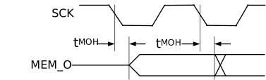
| tMOH | External memory output hold time | 1.0 | ns |