TWIM — I2C compatible two-wire interface master with EasyDMA
TWI master with EasyDMA (TWIM) is a two-wire half-duplex master which can communicate with multiple slave devices connected to the same bus.
- I2C compatible
- Supported baud rates: 100, 250, 400 and 1000 kbps
- Support for clock stretching (non I2C compliant)
- EasyDMA
The two-wire interface can communicate with a bi-directional wired-AND bus with two lines (SCL, SDA). The protocol makes it possible to interconnect up to 127 individually addressable devices. TWIM is not compatible with CBUS.
The GPIOs used for each two-wire interface line can be chosen from any GPIO on the device and are independently configurable. This enables great flexibility in device pinout and efficient use of board space and signal routing.
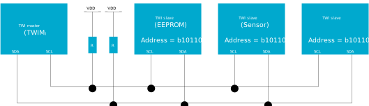
A typical TWI setup consists of one master and one or more slaves, as illustrated in the following figure. TWIM is only able to operate as a single master on the TWI bus. Multi-master bus configuration is not supported.
TWIM supports clock stretching performed by the slaves. The SCK pulse following a stretched clock cycle may be shorter than specified by the I2C specification.
TWIM is started by triggering the STARTTX or STARTRX tasks, and stopped by triggering the STOP task. After a STOP task, TWIM generates a STOPPED event when it has stopped.
After TWIM has been started, the STARTTX or STARTRX tasks should not be triggered again until TWIM has issued a LASTRX, LASTTX, or STOPPED event.
TWIM can be suspended using the SUSPEND task, such as when using the TWI master in a low priority interrupt context. When TWIM enters suspend state, it will automatically issue a SUSPENDED event while performing a continuous clock stretching until it is instructed to resume operation via a RESUME task. TWIM cannot be stopped while it is suspended, thus the STOP task has to be issued after the TWI master has been resumed.
If a NACK is clocked in from the slave, TWIM generates an ERROR event.
Shared resources
TWIM shares registers and other resources with other peripherals that have the same ID as the TWI master. Therefore, you must disable all peripherals that have the same ID as TWIM before it can be configured and used.
Disabling a peripheral that has the same ID as TWIM will not reset any of the registers that are shared with TWIM. It is therefore important to configure all relevant registers explicitly to secure that TWIM operates correctly.
The Instantiation table in Peripherals shows which peripherals have the same ID as the TWI.
EasyDMA
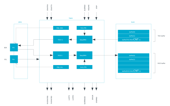
TWIM implements EasyDMA for accessing RAM without CPU involvement.
For detailed information regarding the use of EasyDMA, see EasyDMA.
The RXD.PTR, TXD.PTR, RXD.MAXCNT, and TXD.MAXCNT registers are double-buffered. They can be updated and prepared for the next RX or TX transmission immediately after having received the RXSTARTED or TXSTARTED event.
The STOPPED event indicates that EasyDMA has finished accessing the buffer in RAM.
Master write sequence
A TWIM write sequence is started by triggering the STARTTX task. After the STARTTX task has been triggered, TWIM generates a start condition on the TWI bus, followed by clocking out the address and the READ/WRITE bit set to 0 (WRITE=0, READ=1).
The address must match the address of the slave device that the master wants to write to. The READ/WRITE bit is followed by an ACK/NACK bit (ACK=0 or NACK=1) generated by the slave.
After receiving the ACK bit, TWIM clocks out the data bytes found in the transmit buffer located in RAM at the address specified in the TXD.PTR register. Each byte clocked out from TWIM will be followed by an ACK/NACK bit clocked in from the slave.
A typical TWIM write sequence is shown in the following figure, including clock stretching performed by TWIM following a SUSPEND task.
A SUSPENDED event indicates that the SUSPEND task has taken effect. This event can be used to synchronize the software.
TWIM will generate a LASTTX event when it starts to transmit the last byte.
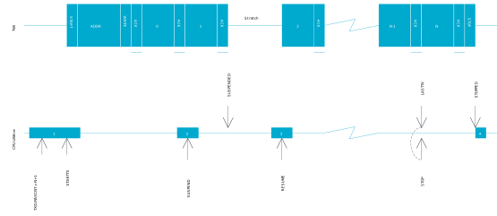
TWIM is stopped by triggering the STOP task. This task should be triggered during the transmission of the last byte to secure that TWIM will stop as fast as possible after sending the last byte. The shortcut between LASTTX and STOP can alternatively be used to accomplish this.
Master read sequence
A TWIM read sequence is started by triggering the STARTRX task. After the STARTRX task has been triggered, TWIM generates a start condition on the TWI bus, followed by clocking out the address and the READ/WRITE bit set to 1 (WRITE = 0, READ = 1). The address must match the address of the slave device that the master wants to read from. The READ/WRITE bit is followed by an ACK/NACK bit (ACK=0 or NACK = 1) generated by the slave.
After sending the ACK bit, the TWI slave sends data to the master using the clock generated by TWIM.
Data received will be stored in RAM at the address specified in the RXD.PTR register. The TWI master will generate an ACK after all but the last byte have been received from the slave. TWIM generates a NACK after the last byte received to indicate that the read sequence shall stop.
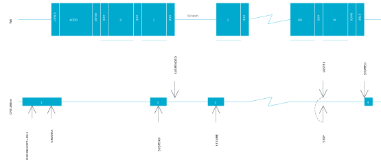
A typical TWIM read sequence is illustrated in the following figure, including clock stretching performed by TWIM following a SUSPEND task.
A SUSPENDED event indicates that the SUSPEND task has taken effect. This event can be used to synchronize the software.
TWIM generates a LASTRX event when it is ready to receive the last byte. If RXD.MAXCNT > 1, the LASTRX event is generated after sending the ACK of the previously received byte. If RXD.MAXCNT = 1, the LASTRX event is generated after receiving the ACK following the address and READ bit.
TWIM is stopped by triggering the STOP task. This task must be triggered before the NACK bit is supposed to be transmitted. The STOP task can be triggered at any time during the reception of the last byte. It is recommended to use the shortcut between LASTRX and STOP to accomplish this.
TWIM does not stop by itself when the RAM buffer is full, or when an error occurs. The STOP task must be issued, through the use of a local or PPI shortcut, or in software as part of the error handler.
TWIM cannot be stopped while suspended, so the STOP task must be issued after TWIM has been resumed.
Master repeated start sequence
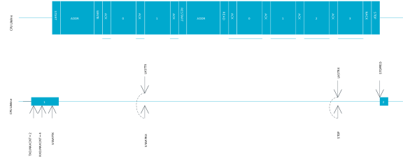
A typical repeated start sequence is when TWIM writes two bytes to the slave followed by reading four bytes from the slave. This example uses shortcuts to perform the simplest type of repeated start sequence, i.e. one write followed by one read. The same approach can be used to perform a repeated start sequence where the sequence is read followed by write.
The following figure shows an example of a repeated start sequence where TWIM writes two bytes followed by reading four bytes from the slave.
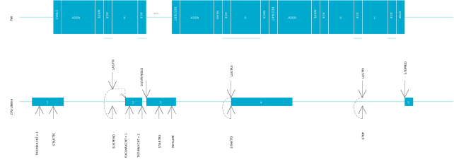
If a more complex repeated start sequence is needed, and the TWI firmware drive is serviced in a low priority interrupt, it may be necessary to use the SUSPEND task and SUSPENDED event to guarantee that the correct tasks are generated at the correct time. A double repeated start sequence using the SUSPEND task to secure safe operation in low priority interrupts is shown in the following figure.
Low power
To ensure lowest possible power consumption when the peripheral is not needed stop and disable TWIM.
When the STOP task is sent, the software shall wait until the STOPPED event is received as a response before disabling the peripheral through the ENABLE register. If the peripheral is already stopped, the STOP task is not required.
Master mode pin configuration
The SCL and SDA signals are mapped to physical pins using the PSEL.SCL and PSEL.SDA registers.
The PSEL.SCL and PSEL.SDA registers and their configurations are only used as long as the TWI master is enabled, and retained only as long as the device is in System ON mode. When the peripheral is disabled, the pins will behave as regular GPIOs, and use the configuration in their respective OUT bit field and PIN_CNF[n] register. PSEL.SCL and PSEL.SDA must only be configured when the TWI master is disabled.
To secure correct signal levels on the pins used by TWIM while in System OFF mode, and when TWIM is disabled, these pins must be configured in the GPIO peripheral as described in the following table.
Only one peripheral can be assigned to drive a particular GPIO pin at a time. Failing to do so may result in unpredictable behavior.
Registers
Instances
| Instance | Domain | Base address | TrustZone | Split access | Description | ||
|---|---|---|---|---|---|---|---|
| Map | Att | DMA | |||||
TWIM0 : S | APPLICATION | 0x50008000 | US | S | SA | No | Two-wire interface master 0 |
TWIM1 : S | APPLICATION | 0x50009000 | US | S | SA | No | Two-wire interface master 1 |
TWIM2 : S | APPLICATION | 0x5000B000 | US | S | SA | No | Two-wire interface master 2 |
TWIM3 : S | APPLICATION | 0x5000C000 | US | S | SA | No | Two-wire interface master 3 |
| TWIM0 | NETWORK | 0x41013000 | HF | NS | NA | No | Two-wire interface master 0 |
Register overview
| Register | Offset | TZ | Description |
|---|---|---|---|
| TASKS_STARTRX | 0x000 | Start TWI receive sequence | |
| TASKS_STARTTX | 0x008 | Start TWI transmit sequence | |
| TASKS_STOP | 0x014 | Stop TWI transaction. Must be issued while the TWI master is not suspended. | |
| TASKS_SUSPEND | 0x01C | Suspend TWI transaction | |
| TASKS_RESUME | 0x020 | Resume TWI transaction | |
| SUBSCRIBE_STARTRX | 0x080 | Subscribe configuration for task STARTRX | |
| SUBSCRIBE_STARTTX | 0x088 | Subscribe configuration for task STARTTX | |
| SUBSCRIBE_STOP | 0x094 | Subscribe configuration for task STOP | |
| SUBSCRIBE_SUSPEND | 0x09C | Subscribe configuration for task SUSPEND | |
| SUBSCRIBE_RESUME | 0x0A0 | Subscribe configuration for task RESUME | |
| EVENTS_STOPPED | 0x104 | TWI stopped | |
| EVENTS_ERROR | 0x124 | TWI error | |
| EVENTS_SUSPENDED | 0x148 | SUSPEND task has been issued, TWI traffic is now suspended. | |
| EVENTS_RXSTARTED | 0x14C | Receive sequence started | |
| EVENTS_TXSTARTED | 0x150 | Transmit sequence started | |
| EVENTS_LASTRX | 0x15C | Byte boundary, starting to receive the last byte | |
| EVENTS_LASTTX | 0x160 | Byte boundary, starting to transmit the last byte | |
| PUBLISH_STOPPED | 0x184 | Publish configuration for event STOPPED | |
| PUBLISH_ERROR | 0x1A4 | Publish configuration for event ERROR | |
| PUBLISH_SUSPENDED | 0x1C8 | Publish configuration for event SUSPENDED | |
| PUBLISH_RXSTARTED | 0x1CC | Publish configuration for event RXSTARTED | |
| PUBLISH_TXSTARTED | 0x1D0 | Publish configuration for event TXSTARTED | |
| PUBLISH_LASTRX | 0x1DC | Publish configuration for event LASTRX | |
| PUBLISH_LASTTX | 0x1E0 | Publish configuration for event LASTTX | |
| SHORTS | 0x200 | Shortcuts between local events and tasks | |
| INTEN | 0x300 | Enable or disable interrupt | |
| INTENSET | 0x304 | Enable interrupt | |
| INTENCLR | 0x308 | Disable interrupt | |
| ERRORSRC | 0x4C4 | Error source | |
| ENABLE | 0x500 | Enable TWIM | |
| PSEL.SCL | 0x508 | Pin select for SCL signal | |
| PSEL.SDA | 0x50C | Pin select for SDA signal | |
| FREQUENCY | 0x524 | TWI frequency. Accuracy depends on the HFCLK source selected. | |
| RXD.PTR | 0x534 | Data pointer | |
| RXD.MAXCNT | 0x538 | Maximum number of bytes in receive buffer | |
| RXD.AMOUNT | 0x53C | Number of bytes transferred in the last transaction | |
| RXD.LIST | 0x540 | EasyDMA list type | |
| TXD.PTR | 0x544 | Data pointer | |
| TXD.MAXCNT | 0x548 | Maximum number of bytes in transmit buffer | |
| TXD.AMOUNT | 0x54C | Number of bytes transferred in the last transaction | |
| TXD.LIST | 0x550 | EasyDMA list type | |
| ADDRESS | 0x588 | Address used in the TWI transfer |
TASKS_STARTRX
Address offset: 0x000
Start TWI receive sequence
| Bit number | 31 | 30 | 29 | 28 | 27 | 26 | 25 | 24 | 23 | 22 | 21 | 20 | 19 | 18 | 17 | 16 | 15 | 14 | 13 | 12 | 11 | 10 | 9 | 8 | 7 | 6 | 5 | 4 | 3 | 2 | 1 | 0 | |||
|---|---|---|---|---|---|---|---|---|---|---|---|---|---|---|---|---|---|---|---|---|---|---|---|---|---|---|---|---|---|---|---|---|---|---|---|
| ID | A | ||||||||||||||||||||||||||||||||||
| Reset 0x00000000 | 0 | 0 | 0 | 0 | 0 | 0 | 0 | 0 | 0 | 0 | 0 | 0 | 0 | 0 | 0 | 0 | 0 | 0 | 0 | 0 | 0 | 0 | 0 | 0 | 0 | 0 | 0 | 0 | 0 | 0 | 0 | 0 | |||
| ID | R/W | Field | Value ID | Value | Description | ||||||||||||||||||||||||||||||
| A | W | TASKS_STARTRX | Start TWI receive sequence | ||||||||||||||||||||||||||||||||
Trigger | 1 | Trigger task | |||||||||||||||||||||||||||||||||
TASKS_STARTTX
Address offset: 0x008
Start TWI transmit sequence
| Bit number | 31 | 30 | 29 | 28 | 27 | 26 | 25 | 24 | 23 | 22 | 21 | 20 | 19 | 18 | 17 | 16 | 15 | 14 | 13 | 12 | 11 | 10 | 9 | 8 | 7 | 6 | 5 | 4 | 3 | 2 | 1 | 0 | |||
|---|---|---|---|---|---|---|---|---|---|---|---|---|---|---|---|---|---|---|---|---|---|---|---|---|---|---|---|---|---|---|---|---|---|---|---|
| ID | A | ||||||||||||||||||||||||||||||||||
| Reset 0x00000000 | 0 | 0 | 0 | 0 | 0 | 0 | 0 | 0 | 0 | 0 | 0 | 0 | 0 | 0 | 0 | 0 | 0 | 0 | 0 | 0 | 0 | 0 | 0 | 0 | 0 | 0 | 0 | 0 | 0 | 0 | 0 | 0 | |||
| ID | R/W | Field | Value ID | Value | Description | ||||||||||||||||||||||||||||||
| A | W | TASKS_STARTTX | Start TWI transmit sequence | ||||||||||||||||||||||||||||||||
Trigger | 1 | Trigger task | |||||||||||||||||||||||||||||||||
TASKS_STOP
Address offset: 0x014
Stop TWI transaction. Must be issued while the TWI master is not suspended.
| Bit number | 31 | 30 | 29 | 28 | 27 | 26 | 25 | 24 | 23 | 22 | 21 | 20 | 19 | 18 | 17 | 16 | 15 | 14 | 13 | 12 | 11 | 10 | 9 | 8 | 7 | 6 | 5 | 4 | 3 | 2 | 1 | 0 | |||
|---|---|---|---|---|---|---|---|---|---|---|---|---|---|---|---|---|---|---|---|---|---|---|---|---|---|---|---|---|---|---|---|---|---|---|---|
| ID | A | ||||||||||||||||||||||||||||||||||
| Reset 0x00000000 | 0 | 0 | 0 | 0 | 0 | 0 | 0 | 0 | 0 | 0 | 0 | 0 | 0 | 0 | 0 | 0 | 0 | 0 | 0 | 0 | 0 | 0 | 0 | 0 | 0 | 0 | 0 | 0 | 0 | 0 | 0 | 0 | |||
| ID | R/W | Field | Value ID | Value | Description | ||||||||||||||||||||||||||||||
| A | W | TASKS_STOP | Stop TWI transaction. Must be issued while the TWI master is not suspended. | ||||||||||||||||||||||||||||||||
Trigger | 1 | Trigger task | |||||||||||||||||||||||||||||||||
TASKS_SUSPEND
Address offset: 0x01C
Suspend TWI transaction
| Bit number | 31 | 30 | 29 | 28 | 27 | 26 | 25 | 24 | 23 | 22 | 21 | 20 | 19 | 18 | 17 | 16 | 15 | 14 | 13 | 12 | 11 | 10 | 9 | 8 | 7 | 6 | 5 | 4 | 3 | 2 | 1 | 0 | |||
|---|---|---|---|---|---|---|---|---|---|---|---|---|---|---|---|---|---|---|---|---|---|---|---|---|---|---|---|---|---|---|---|---|---|---|---|
| ID | A | ||||||||||||||||||||||||||||||||||
| Reset 0x00000000 | 0 | 0 | 0 | 0 | 0 | 0 | 0 | 0 | 0 | 0 | 0 | 0 | 0 | 0 | 0 | 0 | 0 | 0 | 0 | 0 | 0 | 0 | 0 | 0 | 0 | 0 | 0 | 0 | 0 | 0 | 0 | 0 | |||
| ID | R/W | Field | Value ID | Value | Description | ||||||||||||||||||||||||||||||
| A | W | TASKS_SUSPEND | Suspend TWI transaction | ||||||||||||||||||||||||||||||||
Trigger | 1 | Trigger task | |||||||||||||||||||||||||||||||||
TASKS_RESUME
Address offset: 0x020
Resume TWI transaction
| Bit number | 31 | 30 | 29 | 28 | 27 | 26 | 25 | 24 | 23 | 22 | 21 | 20 | 19 | 18 | 17 | 16 | 15 | 14 | 13 | 12 | 11 | 10 | 9 | 8 | 7 | 6 | 5 | 4 | 3 | 2 | 1 | 0 | |||
|---|---|---|---|---|---|---|---|---|---|---|---|---|---|---|---|---|---|---|---|---|---|---|---|---|---|---|---|---|---|---|---|---|---|---|---|
| ID | A | ||||||||||||||||||||||||||||||||||
| Reset 0x00000000 | 0 | 0 | 0 | 0 | 0 | 0 | 0 | 0 | 0 | 0 | 0 | 0 | 0 | 0 | 0 | 0 | 0 | 0 | 0 | 0 | 0 | 0 | 0 | 0 | 0 | 0 | 0 | 0 | 0 | 0 | 0 | 0 | |||
| ID | R/W | Field | Value ID | Value | Description | ||||||||||||||||||||||||||||||
| A | W | TASKS_RESUME | Resume TWI transaction | ||||||||||||||||||||||||||||||||
Trigger | 1 | Trigger task | |||||||||||||||||||||||||||||||||
SUBSCRIBE_STARTRX
Address offset: 0x080
Subscribe configuration for task STARTRX
| Bit number | 31 | 30 | 29 | 28 | 27 | 26 | 25 | 24 | 23 | 22 | 21 | 20 | 19 | 18 | 17 | 16 | 15 | 14 | 13 | 12 | 11 | 10 | 9 | 8 | 7 | 6 | 5 | 4 | 3 | 2 | 1 | 0 | |||
|---|---|---|---|---|---|---|---|---|---|---|---|---|---|---|---|---|---|---|---|---|---|---|---|---|---|---|---|---|---|---|---|---|---|---|---|
| ID | B | A | A | A | A | A | A | A | A | ||||||||||||||||||||||||||
| Reset 0x00000000 | 0 | 0 | 0 | 0 | 0 | 0 | 0 | 0 | 0 | 0 | 0 | 0 | 0 | 0 | 0 | 0 | 0 | 0 | 0 | 0 | 0 | 0 | 0 | 0 | 0 | 0 | 0 | 0 | 0 | 0 | 0 | 0 | |||
| ID | R/W | Field | Value ID | Value | Description | ||||||||||||||||||||||||||||||
| A | RW | CHIDX | [0..255] | DPPI channel that task STARTRX will subscribe to | |||||||||||||||||||||||||||||||
| B | RW | EN | |||||||||||||||||||||||||||||||||
Disabled | 0 | Disable subscription | |||||||||||||||||||||||||||||||||
Enabled | 1 | Enable subscription | |||||||||||||||||||||||||||||||||
SUBSCRIBE_STARTTX
Address offset: 0x088
Subscribe configuration for task STARTTX
| Bit number | 31 | 30 | 29 | 28 | 27 | 26 | 25 | 24 | 23 | 22 | 21 | 20 | 19 | 18 | 17 | 16 | 15 | 14 | 13 | 12 | 11 | 10 | 9 | 8 | 7 | 6 | 5 | 4 | 3 | 2 | 1 | 0 | |||
|---|---|---|---|---|---|---|---|---|---|---|---|---|---|---|---|---|---|---|---|---|---|---|---|---|---|---|---|---|---|---|---|---|---|---|---|
| ID | B | A | A | A | A | A | A | A | A | ||||||||||||||||||||||||||
| Reset 0x00000000 | 0 | 0 | 0 | 0 | 0 | 0 | 0 | 0 | 0 | 0 | 0 | 0 | 0 | 0 | 0 | 0 | 0 | 0 | 0 | 0 | 0 | 0 | 0 | 0 | 0 | 0 | 0 | 0 | 0 | 0 | 0 | 0 | |||
| ID | R/W | Field | Value ID | Value | Description | ||||||||||||||||||||||||||||||
| A | RW | CHIDX | [0..255] | DPPI channel that task STARTTX will subscribe to | |||||||||||||||||||||||||||||||
| B | RW | EN | |||||||||||||||||||||||||||||||||
Disabled | 0 | Disable subscription | |||||||||||||||||||||||||||||||||
Enabled | 1 | Enable subscription | |||||||||||||||||||||||||||||||||
SUBSCRIBE_STOP
Address offset: 0x094
Subscribe configuration for task STOP
| Bit number | 31 | 30 | 29 | 28 | 27 | 26 | 25 | 24 | 23 | 22 | 21 | 20 | 19 | 18 | 17 | 16 | 15 | 14 | 13 | 12 | 11 | 10 | 9 | 8 | 7 | 6 | 5 | 4 | 3 | 2 | 1 | 0 | |||
|---|---|---|---|---|---|---|---|---|---|---|---|---|---|---|---|---|---|---|---|---|---|---|---|---|---|---|---|---|---|---|---|---|---|---|---|
| ID | B | A | A | A | A | A | A | A | A | ||||||||||||||||||||||||||
| Reset 0x00000000 | 0 | 0 | 0 | 0 | 0 | 0 | 0 | 0 | 0 | 0 | 0 | 0 | 0 | 0 | 0 | 0 | 0 | 0 | 0 | 0 | 0 | 0 | 0 | 0 | 0 | 0 | 0 | 0 | 0 | 0 | 0 | 0 | |||
| ID | R/W | Field | Value ID | Value | Description | ||||||||||||||||||||||||||||||
| A | RW | CHIDX | [0..255] | DPPI channel that task STOP will subscribe to | |||||||||||||||||||||||||||||||
| B | RW | EN | |||||||||||||||||||||||||||||||||
Disabled | 0 | Disable subscription | |||||||||||||||||||||||||||||||||
Enabled | 1 | Enable subscription | |||||||||||||||||||||||||||||||||
SUBSCRIBE_SUSPEND
Address offset: 0x09C
Subscribe configuration for task SUSPEND
| Bit number | 31 | 30 | 29 | 28 | 27 | 26 | 25 | 24 | 23 | 22 | 21 | 20 | 19 | 18 | 17 | 16 | 15 | 14 | 13 | 12 | 11 | 10 | 9 | 8 | 7 | 6 | 5 | 4 | 3 | 2 | 1 | 0 | |||
|---|---|---|---|---|---|---|---|---|---|---|---|---|---|---|---|---|---|---|---|---|---|---|---|---|---|---|---|---|---|---|---|---|---|---|---|
| ID | B | A | A | A | A | A | A | A | A | ||||||||||||||||||||||||||
| Reset 0x00000000 | 0 | 0 | 0 | 0 | 0 | 0 | 0 | 0 | 0 | 0 | 0 | 0 | 0 | 0 | 0 | 0 | 0 | 0 | 0 | 0 | 0 | 0 | 0 | 0 | 0 | 0 | 0 | 0 | 0 | 0 | 0 | 0 | |||
| ID | R/W | Field | Value ID | Value | Description | ||||||||||||||||||||||||||||||
| A | RW | CHIDX | [0..255] | DPPI channel that task SUSPEND will subscribe to | |||||||||||||||||||||||||||||||
| B | RW | EN | |||||||||||||||||||||||||||||||||
Disabled | 0 | Disable subscription | |||||||||||||||||||||||||||||||||
Enabled | 1 | Enable subscription | |||||||||||||||||||||||||||||||||
SUBSCRIBE_RESUME
Address offset: 0x0A0
Subscribe configuration for task RESUME
| Bit number | 31 | 30 | 29 | 28 | 27 | 26 | 25 | 24 | 23 | 22 | 21 | 20 | 19 | 18 | 17 | 16 | 15 | 14 | 13 | 12 | 11 | 10 | 9 | 8 | 7 | 6 | 5 | 4 | 3 | 2 | 1 | 0 | |||
|---|---|---|---|---|---|---|---|---|---|---|---|---|---|---|---|---|---|---|---|---|---|---|---|---|---|---|---|---|---|---|---|---|---|---|---|
| ID | B | A | A | A | A | A | A | A | A | ||||||||||||||||||||||||||
| Reset 0x00000000 | 0 | 0 | 0 | 0 | 0 | 0 | 0 | 0 | 0 | 0 | 0 | 0 | 0 | 0 | 0 | 0 | 0 | 0 | 0 | 0 | 0 | 0 | 0 | 0 | 0 | 0 | 0 | 0 | 0 | 0 | 0 | 0 | |||
| ID | R/W | Field | Value ID | Value | Description | ||||||||||||||||||||||||||||||
| A | RW | CHIDX | [0..255] | DPPI channel that task RESUME will subscribe to | |||||||||||||||||||||||||||||||
| B | RW | EN | |||||||||||||||||||||||||||||||||
Disabled | 0 | Disable subscription | |||||||||||||||||||||||||||||||||
Enabled | 1 | Enable subscription | |||||||||||||||||||||||||||||||||
EVENTS_STOPPED
Address offset: 0x104
TWI stopped
| Bit number | 31 | 30 | 29 | 28 | 27 | 26 | 25 | 24 | 23 | 22 | 21 | 20 | 19 | 18 | 17 | 16 | 15 | 14 | 13 | 12 | 11 | 10 | 9 | 8 | 7 | 6 | 5 | 4 | 3 | 2 | 1 | 0 | |||
|---|---|---|---|---|---|---|---|---|---|---|---|---|---|---|---|---|---|---|---|---|---|---|---|---|---|---|---|---|---|---|---|---|---|---|---|
| ID | A | ||||||||||||||||||||||||||||||||||
| Reset 0x00000000 | 0 | 0 | 0 | 0 | 0 | 0 | 0 | 0 | 0 | 0 | 0 | 0 | 0 | 0 | 0 | 0 | 0 | 0 | 0 | 0 | 0 | 0 | 0 | 0 | 0 | 0 | 0 | 0 | 0 | 0 | 0 | 0 | |||
| ID | R/W | Field | Value ID | Value | Description | ||||||||||||||||||||||||||||||
| A | RW | EVENTS_STOPPED | TWI stopped | ||||||||||||||||||||||||||||||||
NotGenerated | 0 | Event not generated | |||||||||||||||||||||||||||||||||
Generated | 1 | Event generated | |||||||||||||||||||||||||||||||||
EVENTS_ERROR
Address offset: 0x124
TWI error
| Bit number | 31 | 30 | 29 | 28 | 27 | 26 | 25 | 24 | 23 | 22 | 21 | 20 | 19 | 18 | 17 | 16 | 15 | 14 | 13 | 12 | 11 | 10 | 9 | 8 | 7 | 6 | 5 | 4 | 3 | 2 | 1 | 0 | |||
|---|---|---|---|---|---|---|---|---|---|---|---|---|---|---|---|---|---|---|---|---|---|---|---|---|---|---|---|---|---|---|---|---|---|---|---|
| ID | A | ||||||||||||||||||||||||||||||||||
| Reset 0x00000000 | 0 | 0 | 0 | 0 | 0 | 0 | 0 | 0 | 0 | 0 | 0 | 0 | 0 | 0 | 0 | 0 | 0 | 0 | 0 | 0 | 0 | 0 | 0 | 0 | 0 | 0 | 0 | 0 | 0 | 0 | 0 | 0 | |||
| ID | R/W | Field | Value ID | Value | Description | ||||||||||||||||||||||||||||||
| A | RW | EVENTS_ERROR | TWI error | ||||||||||||||||||||||||||||||||
NotGenerated | 0 | Event not generated | |||||||||||||||||||||||||||||||||
Generated | 1 | Event generated | |||||||||||||||||||||||||||||||||
EVENTS_SUSPENDED
Address offset: 0x148
SUSPEND task has been issued, TWI traffic is now suspended.
| Bit number | 31 | 30 | 29 | 28 | 27 | 26 | 25 | 24 | 23 | 22 | 21 | 20 | 19 | 18 | 17 | 16 | 15 | 14 | 13 | 12 | 11 | 10 | 9 | 8 | 7 | 6 | 5 | 4 | 3 | 2 | 1 | 0 | |||
|---|---|---|---|---|---|---|---|---|---|---|---|---|---|---|---|---|---|---|---|---|---|---|---|---|---|---|---|---|---|---|---|---|---|---|---|
| ID | A | ||||||||||||||||||||||||||||||||||
| Reset 0x00000000 | 0 | 0 | 0 | 0 | 0 | 0 | 0 | 0 | 0 | 0 | 0 | 0 | 0 | 0 | 0 | 0 | 0 | 0 | 0 | 0 | 0 | 0 | 0 | 0 | 0 | 0 | 0 | 0 | 0 | 0 | 0 | 0 | |||
| ID | R/W | Field | Value ID | Value | Description | ||||||||||||||||||||||||||||||
| A | RW | EVENTS_SUSPENDED | SUSPEND task has been issued, TWI traffic is now suspended. | ||||||||||||||||||||||||||||||||
NotGenerated | 0 | Event not generated | |||||||||||||||||||||||||||||||||
Generated | 1 | Event generated | |||||||||||||||||||||||||||||||||
EVENTS_RXSTARTED
Address offset: 0x14C
Receive sequence started
| Bit number | 31 | 30 | 29 | 28 | 27 | 26 | 25 | 24 | 23 | 22 | 21 | 20 | 19 | 18 | 17 | 16 | 15 | 14 | 13 | 12 | 11 | 10 | 9 | 8 | 7 | 6 | 5 | 4 | 3 | 2 | 1 | 0 | |||
|---|---|---|---|---|---|---|---|---|---|---|---|---|---|---|---|---|---|---|---|---|---|---|---|---|---|---|---|---|---|---|---|---|---|---|---|
| ID | A | ||||||||||||||||||||||||||||||||||
| Reset 0x00000000 | 0 | 0 | 0 | 0 | 0 | 0 | 0 | 0 | 0 | 0 | 0 | 0 | 0 | 0 | 0 | 0 | 0 | 0 | 0 | 0 | 0 | 0 | 0 | 0 | 0 | 0 | 0 | 0 | 0 | 0 | 0 | 0 | |||
| ID | R/W | Field | Value ID | Value | Description | ||||||||||||||||||||||||||||||
| A | RW | EVENTS_RXSTARTED | Receive sequence started | ||||||||||||||||||||||||||||||||
NotGenerated | 0 | Event not generated | |||||||||||||||||||||||||||||||||
Generated | 1 | Event generated | |||||||||||||||||||||||||||||||||
EVENTS_TXSTARTED
Address offset: 0x150
Transmit sequence started
| Bit number | 31 | 30 | 29 | 28 | 27 | 26 | 25 | 24 | 23 | 22 | 21 | 20 | 19 | 18 | 17 | 16 | 15 | 14 | 13 | 12 | 11 | 10 | 9 | 8 | 7 | 6 | 5 | 4 | 3 | 2 | 1 | 0 | |||
|---|---|---|---|---|---|---|---|---|---|---|---|---|---|---|---|---|---|---|---|---|---|---|---|---|---|---|---|---|---|---|---|---|---|---|---|
| ID | A | ||||||||||||||||||||||||||||||||||
| Reset 0x00000000 | 0 | 0 | 0 | 0 | 0 | 0 | 0 | 0 | 0 | 0 | 0 | 0 | 0 | 0 | 0 | 0 | 0 | 0 | 0 | 0 | 0 | 0 | 0 | 0 | 0 | 0 | 0 | 0 | 0 | 0 | 0 | 0 | |||
| ID | R/W | Field | Value ID | Value | Description | ||||||||||||||||||||||||||||||
| A | RW | EVENTS_TXSTARTED | Transmit sequence started | ||||||||||||||||||||||||||||||||
NotGenerated | 0 | Event not generated | |||||||||||||||||||||||||||||||||
Generated | 1 | Event generated | |||||||||||||||||||||||||||||||||
EVENTS_LASTRX
Address offset: 0x15C
Byte boundary, starting to receive the last byte
| Bit number | 31 | 30 | 29 | 28 | 27 | 26 | 25 | 24 | 23 | 22 | 21 | 20 | 19 | 18 | 17 | 16 | 15 | 14 | 13 | 12 | 11 | 10 | 9 | 8 | 7 | 6 | 5 | 4 | 3 | 2 | 1 | 0 | |||
|---|---|---|---|---|---|---|---|---|---|---|---|---|---|---|---|---|---|---|---|---|---|---|---|---|---|---|---|---|---|---|---|---|---|---|---|
| ID | A | ||||||||||||||||||||||||||||||||||
| Reset 0x00000000 | 0 | 0 | 0 | 0 | 0 | 0 | 0 | 0 | 0 | 0 | 0 | 0 | 0 | 0 | 0 | 0 | 0 | 0 | 0 | 0 | 0 | 0 | 0 | 0 | 0 | 0 | 0 | 0 | 0 | 0 | 0 | 0 | |||
| ID | R/W | Field | Value ID | Value | Description | ||||||||||||||||||||||||||||||
| A | RW | EVENTS_LASTRX | Byte boundary, starting to receive the last byte | ||||||||||||||||||||||||||||||||
NotGenerated | 0 | Event not generated | |||||||||||||||||||||||||||||||||
Generated | 1 | Event generated | |||||||||||||||||||||||||||||||||
EVENTS_LASTTX
Address offset: 0x160
Byte boundary, starting to transmit the last byte
| Bit number | 31 | 30 | 29 | 28 | 27 | 26 | 25 | 24 | 23 | 22 | 21 | 20 | 19 | 18 | 17 | 16 | 15 | 14 | 13 | 12 | 11 | 10 | 9 | 8 | 7 | 6 | 5 | 4 | 3 | 2 | 1 | 0 | |||
|---|---|---|---|---|---|---|---|---|---|---|---|---|---|---|---|---|---|---|---|---|---|---|---|---|---|---|---|---|---|---|---|---|---|---|---|
| ID | A | ||||||||||||||||||||||||||||||||||
| Reset 0x00000000 | 0 | 0 | 0 | 0 | 0 | 0 | 0 | 0 | 0 | 0 | 0 | 0 | 0 | 0 | 0 | 0 | 0 | 0 | 0 | 0 | 0 | 0 | 0 | 0 | 0 | 0 | 0 | 0 | 0 | 0 | 0 | 0 | |||
| ID | R/W | Field | Value ID | Value | Description | ||||||||||||||||||||||||||||||
| A | RW | EVENTS_LASTTX | Byte boundary, starting to transmit the last byte | ||||||||||||||||||||||||||||||||
NotGenerated | 0 | Event not generated | |||||||||||||||||||||||||||||||||
Generated | 1 | Event generated | |||||||||||||||||||||||||||||||||
PUBLISH_STOPPED
Address offset: 0x184
Publish configuration for event STOPPED
| Bit number | 31 | 30 | 29 | 28 | 27 | 26 | 25 | 24 | 23 | 22 | 21 | 20 | 19 | 18 | 17 | 16 | 15 | 14 | 13 | 12 | 11 | 10 | 9 | 8 | 7 | 6 | 5 | 4 | 3 | 2 | 1 | 0 | |||
|---|---|---|---|---|---|---|---|---|---|---|---|---|---|---|---|---|---|---|---|---|---|---|---|---|---|---|---|---|---|---|---|---|---|---|---|
| ID | B | A | A | A | A | A | A | A | A | ||||||||||||||||||||||||||
| Reset 0x00000000 | 0 | 0 | 0 | 0 | 0 | 0 | 0 | 0 | 0 | 0 | 0 | 0 | 0 | 0 | 0 | 0 | 0 | 0 | 0 | 0 | 0 | 0 | 0 | 0 | 0 | 0 | 0 | 0 | 0 | 0 | 0 | 0 | |||
| ID | R/W | Field | Value ID | Value | Description | ||||||||||||||||||||||||||||||
| A | RW | CHIDX | [0..255] | DPPI channel that event STOPPED will publish to | |||||||||||||||||||||||||||||||
| B | RW | EN | |||||||||||||||||||||||||||||||||
Disabled | 0 | Disable publishing | |||||||||||||||||||||||||||||||||
Enabled | 1 | Enable publishing | |||||||||||||||||||||||||||||||||
PUBLISH_ERROR
Address offset: 0x1A4
Publish configuration for event ERROR
| Bit number | 31 | 30 | 29 | 28 | 27 | 26 | 25 | 24 | 23 | 22 | 21 | 20 | 19 | 18 | 17 | 16 | 15 | 14 | 13 | 12 | 11 | 10 | 9 | 8 | 7 | 6 | 5 | 4 | 3 | 2 | 1 | 0 | |||
|---|---|---|---|---|---|---|---|---|---|---|---|---|---|---|---|---|---|---|---|---|---|---|---|---|---|---|---|---|---|---|---|---|---|---|---|
| ID | B | A | A | A | A | A | A | A | A | ||||||||||||||||||||||||||
| Reset 0x00000000 | 0 | 0 | 0 | 0 | 0 | 0 | 0 | 0 | 0 | 0 | 0 | 0 | 0 | 0 | 0 | 0 | 0 | 0 | 0 | 0 | 0 | 0 | 0 | 0 | 0 | 0 | 0 | 0 | 0 | 0 | 0 | 0 | |||
| ID | R/W | Field | Value ID | Value | Description | ||||||||||||||||||||||||||||||
| A | RW | CHIDX | [0..255] | DPPI channel that event ERROR will publish to | |||||||||||||||||||||||||||||||
| B | RW | EN | |||||||||||||||||||||||||||||||||
Disabled | 0 | Disable publishing | |||||||||||||||||||||||||||||||||
Enabled | 1 | Enable publishing | |||||||||||||||||||||||||||||||||
PUBLISH_SUSPENDED
Address offset: 0x1C8
Publish configuration for event SUSPENDED
| Bit number | 31 | 30 | 29 | 28 | 27 | 26 | 25 | 24 | 23 | 22 | 21 | 20 | 19 | 18 | 17 | 16 | 15 | 14 | 13 | 12 | 11 | 10 | 9 | 8 | 7 | 6 | 5 | 4 | 3 | 2 | 1 | 0 | |||
|---|---|---|---|---|---|---|---|---|---|---|---|---|---|---|---|---|---|---|---|---|---|---|---|---|---|---|---|---|---|---|---|---|---|---|---|
| ID | B | A | A | A | A | A | A | A | A | ||||||||||||||||||||||||||
| Reset 0x00000000 | 0 | 0 | 0 | 0 | 0 | 0 | 0 | 0 | 0 | 0 | 0 | 0 | 0 | 0 | 0 | 0 | 0 | 0 | 0 | 0 | 0 | 0 | 0 | 0 | 0 | 0 | 0 | 0 | 0 | 0 | 0 | 0 | |||
| ID | R/W | Field | Value ID | Value | Description | ||||||||||||||||||||||||||||||
| A | RW | CHIDX | [0..255] | DPPI channel that event SUSPENDED will publish to | |||||||||||||||||||||||||||||||
| B | RW | EN | |||||||||||||||||||||||||||||||||
Disabled | 0 | Disable publishing | |||||||||||||||||||||||||||||||||
Enabled | 1 | Enable publishing | |||||||||||||||||||||||||||||||||
PUBLISH_RXSTARTED
Address offset: 0x1CC
Publish configuration for event RXSTARTED
| Bit number | 31 | 30 | 29 | 28 | 27 | 26 | 25 | 24 | 23 | 22 | 21 | 20 | 19 | 18 | 17 | 16 | 15 | 14 | 13 | 12 | 11 | 10 | 9 | 8 | 7 | 6 | 5 | 4 | 3 | 2 | 1 | 0 | |||
|---|---|---|---|---|---|---|---|---|---|---|---|---|---|---|---|---|---|---|---|---|---|---|---|---|---|---|---|---|---|---|---|---|---|---|---|
| ID | B | A | A | A | A | A | A | A | A | ||||||||||||||||||||||||||
| Reset 0x00000000 | 0 | 0 | 0 | 0 | 0 | 0 | 0 | 0 | 0 | 0 | 0 | 0 | 0 | 0 | 0 | 0 | 0 | 0 | 0 | 0 | 0 | 0 | 0 | 0 | 0 | 0 | 0 | 0 | 0 | 0 | 0 | 0 | |||
| ID | R/W | Field | Value ID | Value | Description | ||||||||||||||||||||||||||||||
| A | RW | CHIDX | [0..255] | DPPI channel that event RXSTARTED will publish to | |||||||||||||||||||||||||||||||
| B | RW | EN | |||||||||||||||||||||||||||||||||
Disabled | 0 | Disable publishing | |||||||||||||||||||||||||||||||||
Enabled | 1 | Enable publishing | |||||||||||||||||||||||||||||||||
PUBLISH_TXSTARTED
Address offset: 0x1D0
Publish configuration for event TXSTARTED
| Bit number | 31 | 30 | 29 | 28 | 27 | 26 | 25 | 24 | 23 | 22 | 21 | 20 | 19 | 18 | 17 | 16 | 15 | 14 | 13 | 12 | 11 | 10 | 9 | 8 | 7 | 6 | 5 | 4 | 3 | 2 | 1 | 0 | |||
|---|---|---|---|---|---|---|---|---|---|---|---|---|---|---|---|---|---|---|---|---|---|---|---|---|---|---|---|---|---|---|---|---|---|---|---|
| ID | B | A | A | A | A | A | A | A | A | ||||||||||||||||||||||||||
| Reset 0x00000000 | 0 | 0 | 0 | 0 | 0 | 0 | 0 | 0 | 0 | 0 | 0 | 0 | 0 | 0 | 0 | 0 | 0 | 0 | 0 | 0 | 0 | 0 | 0 | 0 | 0 | 0 | 0 | 0 | 0 | 0 | 0 | 0 | |||
| ID | R/W | Field | Value ID | Value | Description | ||||||||||||||||||||||||||||||
| A | RW | CHIDX | [0..255] | DPPI channel that event TXSTARTED will publish to | |||||||||||||||||||||||||||||||
| B | RW | EN | |||||||||||||||||||||||||||||||||
Disabled | 0 | Disable publishing | |||||||||||||||||||||||||||||||||
Enabled | 1 | Enable publishing | |||||||||||||||||||||||||||||||||
PUBLISH_LASTRX
Address offset: 0x1DC
Publish configuration for event LASTRX
| Bit number | 31 | 30 | 29 | 28 | 27 | 26 | 25 | 24 | 23 | 22 | 21 | 20 | 19 | 18 | 17 | 16 | 15 | 14 | 13 | 12 | 11 | 10 | 9 | 8 | 7 | 6 | 5 | 4 | 3 | 2 | 1 | 0 | |||
|---|---|---|---|---|---|---|---|---|---|---|---|---|---|---|---|---|---|---|---|---|---|---|---|---|---|---|---|---|---|---|---|---|---|---|---|
| ID | B | A | A | A | A | A | A | A | A | ||||||||||||||||||||||||||
| Reset 0x00000000 | 0 | 0 | 0 | 0 | 0 | 0 | 0 | 0 | 0 | 0 | 0 | 0 | 0 | 0 | 0 | 0 | 0 | 0 | 0 | 0 | 0 | 0 | 0 | 0 | 0 | 0 | 0 | 0 | 0 | 0 | 0 | 0 | |||
| ID | R/W | Field | Value ID | Value | Description | ||||||||||||||||||||||||||||||
| A | RW | CHIDX | [0..255] | DPPI channel that event LASTRX will publish to | |||||||||||||||||||||||||||||||
| B | RW | EN | |||||||||||||||||||||||||||||||||
Disabled | 0 | Disable publishing | |||||||||||||||||||||||||||||||||
Enabled | 1 | Enable publishing | |||||||||||||||||||||||||||||||||
PUBLISH_LASTTX
Address offset: 0x1E0
Publish configuration for event LASTTX
| Bit number | 31 | 30 | 29 | 28 | 27 | 26 | 25 | 24 | 23 | 22 | 21 | 20 | 19 | 18 | 17 | 16 | 15 | 14 | 13 | 12 | 11 | 10 | 9 | 8 | 7 | 6 | 5 | 4 | 3 | 2 | 1 | 0 | |||
|---|---|---|---|---|---|---|---|---|---|---|---|---|---|---|---|---|---|---|---|---|---|---|---|---|---|---|---|---|---|---|---|---|---|---|---|
| ID | B | A | A | A | A | A | A | A | A | ||||||||||||||||||||||||||
| Reset 0x00000000 | 0 | 0 | 0 | 0 | 0 | 0 | 0 | 0 | 0 | 0 | 0 | 0 | 0 | 0 | 0 | 0 | 0 | 0 | 0 | 0 | 0 | 0 | 0 | 0 | 0 | 0 | 0 | 0 | 0 | 0 | 0 | 0 | |||
| ID | R/W | Field | Value ID | Value | Description | ||||||||||||||||||||||||||||||
| A | RW | CHIDX | [0..255] | DPPI channel that event LASTTX will publish to | |||||||||||||||||||||||||||||||
| B | RW | EN | |||||||||||||||||||||||||||||||||
Disabled | 0 | Disable publishing | |||||||||||||||||||||||||||||||||
Enabled | 1 | Enable publishing | |||||||||||||||||||||||||||||||||
SHORTS
Address offset: 0x200
Shortcuts between local events and tasks
| Bit number | 31 | 30 | 29 | 28 | 27 | 26 | 25 | 24 | 23 | 22 | 21 | 20 | 19 | 18 | 17 | 16 | 15 | 14 | 13 | 12 | 11 | 10 | 9 | 8 | 7 | 6 | 5 | 4 | 3 | 2 | 1 | 0 | |||
|---|---|---|---|---|---|---|---|---|---|---|---|---|---|---|---|---|---|---|---|---|---|---|---|---|---|---|---|---|---|---|---|---|---|---|---|
| ID | F | D | C | B | A | ||||||||||||||||||||||||||||||
| Reset 0x00000000 | 0 | 0 | 0 | 0 | 0 | 0 | 0 | 0 | 0 | 0 | 0 | 0 | 0 | 0 | 0 | 0 | 0 | 0 | 0 | 0 | 0 | 0 | 0 | 0 | 0 | 0 | 0 | 0 | 0 | 0 | 0 | 0 | |||
| ID | R/W | Field | Value ID | Value | Description | ||||||||||||||||||||||||||||||
| A | RW | LASTTX_STARTRX | |||||||||||||||||||||||||||||||||
Disabled | 0 | Disable shortcut | |||||||||||||||||||||||||||||||||
Enabled | 1 | Enable shortcut | |||||||||||||||||||||||||||||||||
| B | RW | LASTTX_SUSPEND | |||||||||||||||||||||||||||||||||
Disabled | 0 | Disable shortcut | |||||||||||||||||||||||||||||||||
Enabled | 1 | Enable shortcut | |||||||||||||||||||||||||||||||||
| C | RW | LASTTX_STOP | |||||||||||||||||||||||||||||||||
Disabled | 0 | Disable shortcut | |||||||||||||||||||||||||||||||||
Enabled | 1 | Enable shortcut | |||||||||||||||||||||||||||||||||
| D | RW | LASTRX_STARTTX | |||||||||||||||||||||||||||||||||
Disabled | 0 | Disable shortcut | |||||||||||||||||||||||||||||||||
Enabled | 1 | Enable shortcut | |||||||||||||||||||||||||||||||||
| F | RW | LASTRX_STOP | |||||||||||||||||||||||||||||||||
Disabled | 0 | Disable shortcut | |||||||||||||||||||||||||||||||||
Enabled | 1 | Enable shortcut | |||||||||||||||||||||||||||||||||
INTEN
Address offset: 0x300
Enable or disable interrupt
| Bit number | 31 | 30 | 29 | 28 | 27 | 26 | 25 | 24 | 23 | 22 | 21 | 20 | 19 | 18 | 17 | 16 | 15 | 14 | 13 | 12 | 11 | 10 | 9 | 8 | 7 | 6 | 5 | 4 | 3 | 2 | 1 | 0 | |||
|---|---|---|---|---|---|---|---|---|---|---|---|---|---|---|---|---|---|---|---|---|---|---|---|---|---|---|---|---|---|---|---|---|---|---|---|
| ID | J | I | H | G | F | D | A | ||||||||||||||||||||||||||||
| Reset 0x00000000 | 0 | 0 | 0 | 0 | 0 | 0 | 0 | 0 | 0 | 0 | 0 | 0 | 0 | 0 | 0 | 0 | 0 | 0 | 0 | 0 | 0 | 0 | 0 | 0 | 0 | 0 | 0 | 0 | 0 | 0 | 0 | 0 | |||
| ID | R/W | Field | Value ID | Value | Description | ||||||||||||||||||||||||||||||
| A | RW | STOPPED | Enable or disable interrupt for event STOPPED | ||||||||||||||||||||||||||||||||
Disabled | 0 | Disable | |||||||||||||||||||||||||||||||||
Enabled | 1 | Enable | |||||||||||||||||||||||||||||||||
| D | RW | ERROR | Enable or disable interrupt for event ERROR | ||||||||||||||||||||||||||||||||
Disabled | 0 | Disable | |||||||||||||||||||||||||||||||||
Enabled | 1 | Enable | |||||||||||||||||||||||||||||||||
| F | RW | SUSPENDED | Enable or disable interrupt for event SUSPENDED | ||||||||||||||||||||||||||||||||
Disabled | 0 | Disable | |||||||||||||||||||||||||||||||||
Enabled | 1 | Enable | |||||||||||||||||||||||||||||||||
| G | RW | RXSTARTED | Enable or disable interrupt for event RXSTARTED | ||||||||||||||||||||||||||||||||
Disabled | 0 | Disable | |||||||||||||||||||||||||||||||||
Enabled | 1 | Enable | |||||||||||||||||||||||||||||||||
| H | RW | TXSTARTED | Enable or disable interrupt for event TXSTARTED | ||||||||||||||||||||||||||||||||
Disabled | 0 | Disable | |||||||||||||||||||||||||||||||||
Enabled | 1 | Enable | |||||||||||||||||||||||||||||||||
| I | RW | LASTRX | Enable or disable interrupt for event LASTRX | ||||||||||||||||||||||||||||||||
Disabled | 0 | Disable | |||||||||||||||||||||||||||||||||
Enabled | 1 | Enable | |||||||||||||||||||||||||||||||||
| J | RW | LASTTX | Enable or disable interrupt for event LASTTX | ||||||||||||||||||||||||||||||||
Disabled | 0 | Disable | |||||||||||||||||||||||||||||||||
Enabled | 1 | Enable | |||||||||||||||||||||||||||||||||
INTENSET
Address offset: 0x304
Enable interrupt
| Bit number | 31 | 30 | 29 | 28 | 27 | 26 | 25 | 24 | 23 | 22 | 21 | 20 | 19 | 18 | 17 | 16 | 15 | 14 | 13 | 12 | 11 | 10 | 9 | 8 | 7 | 6 | 5 | 4 | 3 | 2 | 1 | 0 | |||
|---|---|---|---|---|---|---|---|---|---|---|---|---|---|---|---|---|---|---|---|---|---|---|---|---|---|---|---|---|---|---|---|---|---|---|---|
| ID | J | I | H | G | F | D | A | ||||||||||||||||||||||||||||
| Reset 0x00000000 | 0 | 0 | 0 | 0 | 0 | 0 | 0 | 0 | 0 | 0 | 0 | 0 | 0 | 0 | 0 | 0 | 0 | 0 | 0 | 0 | 0 | 0 | 0 | 0 | 0 | 0 | 0 | 0 | 0 | 0 | 0 | 0 | |||
| ID | R/W | Field | Value ID | Value | Description | ||||||||||||||||||||||||||||||
| A | RW | STOPPED | Write '1' to enable interrupt for event STOPPED | ||||||||||||||||||||||||||||||||
Set | 1 | Enable | |||||||||||||||||||||||||||||||||
Disabled | 0 | Read: Disabled | |||||||||||||||||||||||||||||||||
Enabled | 1 | Read: Enabled | |||||||||||||||||||||||||||||||||
| D | RW | ERROR | Write '1' to enable interrupt for event ERROR | ||||||||||||||||||||||||||||||||
Set | 1 | Enable | |||||||||||||||||||||||||||||||||
Disabled | 0 | Read: Disabled | |||||||||||||||||||||||||||||||||
Enabled | 1 | Read: Enabled | |||||||||||||||||||||||||||||||||
| F | RW | SUSPENDED | Write '1' to enable interrupt for event SUSPENDED | ||||||||||||||||||||||||||||||||
Set | 1 | Enable | |||||||||||||||||||||||||||||||||
Disabled | 0 | Read: Disabled | |||||||||||||||||||||||||||||||||
Enabled | 1 | Read: Enabled | |||||||||||||||||||||||||||||||||
| G | RW | RXSTARTED | Write '1' to enable interrupt for event RXSTARTED | ||||||||||||||||||||||||||||||||
Set | 1 | Enable | |||||||||||||||||||||||||||||||||
Disabled | 0 | Read: Disabled | |||||||||||||||||||||||||||||||||
Enabled | 1 | Read: Enabled | |||||||||||||||||||||||||||||||||
| H | RW | TXSTARTED | Write '1' to enable interrupt for event TXSTARTED | ||||||||||||||||||||||||||||||||
Set | 1 | Enable | |||||||||||||||||||||||||||||||||
Disabled | 0 | Read: Disabled | |||||||||||||||||||||||||||||||||
Enabled | 1 | Read: Enabled | |||||||||||||||||||||||||||||||||
| I | RW | LASTRX | Write '1' to enable interrupt for event LASTRX | ||||||||||||||||||||||||||||||||
Set | 1 | Enable | |||||||||||||||||||||||||||||||||
Disabled | 0 | Read: Disabled | |||||||||||||||||||||||||||||||||
Enabled | 1 | Read: Enabled | |||||||||||||||||||||||||||||||||
| J | RW | LASTTX | Write '1' to enable interrupt for event LASTTX | ||||||||||||||||||||||||||||||||
Set | 1 | Enable | |||||||||||||||||||||||||||||||||
Disabled | 0 | Read: Disabled | |||||||||||||||||||||||||||||||||
Enabled | 1 | Read: Enabled | |||||||||||||||||||||||||||||||||
INTENCLR
Address offset: 0x308
Disable interrupt
| Bit number | 31 | 30 | 29 | 28 | 27 | 26 | 25 | 24 | 23 | 22 | 21 | 20 | 19 | 18 | 17 | 16 | 15 | 14 | 13 | 12 | 11 | 10 | 9 | 8 | 7 | 6 | 5 | 4 | 3 | 2 | 1 | 0 | |||
|---|---|---|---|---|---|---|---|---|---|---|---|---|---|---|---|---|---|---|---|---|---|---|---|---|---|---|---|---|---|---|---|---|---|---|---|
| ID | J | I | H | G | F | D | A | ||||||||||||||||||||||||||||
| Reset 0x00000000 | 0 | 0 | 0 | 0 | 0 | 0 | 0 | 0 | 0 | 0 | 0 | 0 | 0 | 0 | 0 | 0 | 0 | 0 | 0 | 0 | 0 | 0 | 0 | 0 | 0 | 0 | 0 | 0 | 0 | 0 | 0 | 0 | |||
| ID | R/W | Field | Value ID | Value | Description | ||||||||||||||||||||||||||||||
| A | RW | STOPPED | Write '1' to disable interrupt for event STOPPED | ||||||||||||||||||||||||||||||||
Clear | 1 | Disable | |||||||||||||||||||||||||||||||||
Disabled | 0 | Read: Disabled | |||||||||||||||||||||||||||||||||
Enabled | 1 | Read: Enabled | |||||||||||||||||||||||||||||||||
| D | RW | ERROR | Write '1' to disable interrupt for event ERROR | ||||||||||||||||||||||||||||||||
Clear | 1 | Disable | |||||||||||||||||||||||||||||||||
Disabled | 0 | Read: Disabled | |||||||||||||||||||||||||||||||||
Enabled | 1 | Read: Enabled | |||||||||||||||||||||||||||||||||
| F | RW | SUSPENDED | Write '1' to disable interrupt for event SUSPENDED | ||||||||||||||||||||||||||||||||
Clear | 1 | Disable | |||||||||||||||||||||||||||||||||
Disabled | 0 | Read: Disabled | |||||||||||||||||||||||||||||||||
Enabled | 1 | Read: Enabled | |||||||||||||||||||||||||||||||||
| G | RW | RXSTARTED | Write '1' to disable interrupt for event RXSTARTED | ||||||||||||||||||||||||||||||||
Clear | 1 | Disable | |||||||||||||||||||||||||||||||||
Disabled | 0 | Read: Disabled | |||||||||||||||||||||||||||||||||
Enabled | 1 | Read: Enabled | |||||||||||||||||||||||||||||||||
| H | RW | TXSTARTED | Write '1' to disable interrupt for event TXSTARTED | ||||||||||||||||||||||||||||||||
Clear | 1 | Disable | |||||||||||||||||||||||||||||||||
Disabled | 0 | Read: Disabled | |||||||||||||||||||||||||||||||||
Enabled | 1 | Read: Enabled | |||||||||||||||||||||||||||||||||
| I | RW | LASTRX | Write '1' to disable interrupt for event LASTRX | ||||||||||||||||||||||||||||||||
Clear | 1 | Disable | |||||||||||||||||||||||||||||||||
Disabled | 0 | Read: Disabled | |||||||||||||||||||||||||||||||||
Enabled | 1 | Read: Enabled | |||||||||||||||||||||||||||||||||
| J | RW | LASTTX | Write '1' to disable interrupt for event LASTTX | ||||||||||||||||||||||||||||||||
Clear | 1 | Disable | |||||||||||||||||||||||||||||||||
Disabled | 0 | Read: Disabled | |||||||||||||||||||||||||||||||||
Enabled | 1 | Read: Enabled | |||||||||||||||||||||||||||||||||
ERRORSRC
Address offset: 0x4C4
Error source
| Bit number | 31 | 30 | 29 | 28 | 27 | 26 | 25 | 24 | 23 | 22 | 21 | 20 | 19 | 18 | 17 | 16 | 15 | 14 | 13 | 12 | 11 | 10 | 9 | 8 | 7 | 6 | 5 | 4 | 3 | 2 | 1 | 0 | |||
|---|---|---|---|---|---|---|---|---|---|---|---|---|---|---|---|---|---|---|---|---|---|---|---|---|---|---|---|---|---|---|---|---|---|---|---|
| ID | C | B | A | ||||||||||||||||||||||||||||||||
| Reset 0x00000000 | 0 | 0 | 0 | 0 | 0 | 0 | 0 | 0 | 0 | 0 | 0 | 0 | 0 | 0 | 0 | 0 | 0 | 0 | 0 | 0 | 0 | 0 | 0 | 0 | 0 | 0 | 0 | 0 | 0 | 0 | 0 | 0 | |||
| ID | R/W | Field | Value ID | Value | Description | ||||||||||||||||||||||||||||||
| A | RW | OVERRUN | Overrun error A new byte was received before previous byte got transferred into RXD buffer. (Previous data is lost) | ||||||||||||||||||||||||||||||||
NotReceived | 0 | Error did not occur | |||||||||||||||||||||||||||||||||
Received | 1 | Error occurred | |||||||||||||||||||||||||||||||||
| B | RW | ANACK | NACK received after sending the address (write '1' to clear) | ||||||||||||||||||||||||||||||||
NotReceived | 0 | Error did not occur | |||||||||||||||||||||||||||||||||
Received | 1 | Error occurred | |||||||||||||||||||||||||||||||||
| C | RW | DNACK | NACK received after sending a data byte (write '1' to clear) | ||||||||||||||||||||||||||||||||
NotReceived | 0 | Error did not occur | |||||||||||||||||||||||||||||||||
Received | 1 | Error occurred | |||||||||||||||||||||||||||||||||
ENABLE
Address offset: 0x500
Enable TWIM
| Bit number | 31 | 30 | 29 | 28 | 27 | 26 | 25 | 24 | 23 | 22 | 21 | 20 | 19 | 18 | 17 | 16 | 15 | 14 | 13 | 12 | 11 | 10 | 9 | 8 | 7 | 6 | 5 | 4 | 3 | 2 | 1 | 0 | |||
|---|---|---|---|---|---|---|---|---|---|---|---|---|---|---|---|---|---|---|---|---|---|---|---|---|---|---|---|---|---|---|---|---|---|---|---|
| ID | A | A | A | A | |||||||||||||||||||||||||||||||
| Reset 0x00000000 | 0 | 0 | 0 | 0 | 0 | 0 | 0 | 0 | 0 | 0 | 0 | 0 | 0 | 0 | 0 | 0 | 0 | 0 | 0 | 0 | 0 | 0 | 0 | 0 | 0 | 0 | 0 | 0 | 0 | 0 | 0 | 0 | |||
| ID | R/W | Field | Value ID | Value | Description | ||||||||||||||||||||||||||||||
| A | RW | ENABLE | Enable or disable TWIM | ||||||||||||||||||||||||||||||||
Disabled | 0 | Disable TWIM | |||||||||||||||||||||||||||||||||
Enabled | 6 | Enable TWIM | |||||||||||||||||||||||||||||||||
PSEL.SCL
Address offset: 0x508
Pin select for SCL signal
| Bit number | 31 | 30 | 29 | 28 | 27 | 26 | 25 | 24 | 23 | 22 | 21 | 20 | 19 | 18 | 17 | 16 | 15 | 14 | 13 | 12 | 11 | 10 | 9 | 8 | 7 | 6 | 5 | 4 | 3 | 2 | 1 | 0 | |||
|---|---|---|---|---|---|---|---|---|---|---|---|---|---|---|---|---|---|---|---|---|---|---|---|---|---|---|---|---|---|---|---|---|---|---|---|
| ID | C | B | A | A | A | A | A | ||||||||||||||||||||||||||||
| Reset 0xFFFFFFFF | 1 | 1 | 1 | 1 | 1 | 1 | 1 | 1 | 1 | 1 | 1 | 1 | 1 | 1 | 1 | 1 | 1 | 1 | 1 | 1 | 1 | 1 | 1 | 1 | 1 | 1 | 1 | 1 | 1 | 1 | 1 | 1 | |||
| ID | R/W | Field | Value ID | Value | Description | ||||||||||||||||||||||||||||||
| A | RW | PIN | [0..31] | Pin number | |||||||||||||||||||||||||||||||
| B | RW | PORT | [0..1] | Port number | |||||||||||||||||||||||||||||||
| C | RW | CONNECT | Connection | ||||||||||||||||||||||||||||||||
Disconnected | 1 | Disconnect | |||||||||||||||||||||||||||||||||
Connected | 0 | Connect | |||||||||||||||||||||||||||||||||
PSEL.SDA
Address offset: 0x50C
Pin select for SDA signal
| Bit number | 31 | 30 | 29 | 28 | 27 | 26 | 25 | 24 | 23 | 22 | 21 | 20 | 19 | 18 | 17 | 16 | 15 | 14 | 13 | 12 | 11 | 10 | 9 | 8 | 7 | 6 | 5 | 4 | 3 | 2 | 1 | 0 | |||
|---|---|---|---|---|---|---|---|---|---|---|---|---|---|---|---|---|---|---|---|---|---|---|---|---|---|---|---|---|---|---|---|---|---|---|---|
| ID | C | B | A | A | A | A | A | ||||||||||||||||||||||||||||
| Reset 0xFFFFFFFF | 1 | 1 | 1 | 1 | 1 | 1 | 1 | 1 | 1 | 1 | 1 | 1 | 1 | 1 | 1 | 1 | 1 | 1 | 1 | 1 | 1 | 1 | 1 | 1 | 1 | 1 | 1 | 1 | 1 | 1 | 1 | 1 | |||
| ID | R/W | Field | Value ID | Value | Description | ||||||||||||||||||||||||||||||
| A | RW | PIN | [0..31] | Pin number | |||||||||||||||||||||||||||||||
| B | RW | PORT | [0..1] | Port number | |||||||||||||||||||||||||||||||
| C | RW | CONNECT | Connection | ||||||||||||||||||||||||||||||||
Disconnected | 1 | Disconnect | |||||||||||||||||||||||||||||||||
Connected | 0 | Connect | |||||||||||||||||||||||||||||||||
FREQUENCY
Address offset: 0x524
TWI frequency. Accuracy depends on the HFCLK source selected.
| Bit number | 31 | 30 | 29 | 28 | 27 | 26 | 25 | 24 | 23 | 22 | 21 | 20 | 19 | 18 | 17 | 16 | 15 | 14 | 13 | 12 | 11 | 10 | 9 | 8 | 7 | 6 | 5 | 4 | 3 | 2 | 1 | 0 | |||
|---|---|---|---|---|---|---|---|---|---|---|---|---|---|---|---|---|---|---|---|---|---|---|---|---|---|---|---|---|---|---|---|---|---|---|---|
| ID | A | A | A | A | A | A | A | A | A | A | A | A | A | A | A | A | A | A | A | A | A | A | A | A | A | A | A | A | A | A | A | A | |||
| Reset 0x04000000 | 0 | 0 | 0 | 0 | 0 | 1 | 0 | 0 | 0 | 0 | 0 | 0 | 0 | 0 | 0 | 0 | 0 | 0 | 0 | 0 | 0 | 0 | 0 | 0 | 0 | 0 | 0 | 0 | 0 | 0 | 0 | 0 | |||
| ID | R/W | Field | Value ID | Value | Description | ||||||||||||||||||||||||||||||
| A | RW | FREQUENCY | TWI master clock frequency | ||||||||||||||||||||||||||||||||
K100 | 0x01980000 | 100 kbps | |||||||||||||||||||||||||||||||||
K250 | 0x04000000 | 250 kbps | |||||||||||||||||||||||||||||||||
K400 | 0x06400000 | 400 kbps | |||||||||||||||||||||||||||||||||
K1000 | 0x0FF00000 | 1000 kbps | |||||||||||||||||||||||||||||||||
RXD
RXD EasyDMA channel
RXD.PTR
Address offset: 0x534
Data pointer
| Bit number | 31 | 30 | 29 | 28 | 27 | 26 | 25 | 24 | 23 | 22 | 21 | 20 | 19 | 18 | 17 | 16 | 15 | 14 | 13 | 12 | 11 | 10 | 9 | 8 | 7 | 6 | 5 | 4 | 3 | 2 | 1 | 0 | |||
|---|---|---|---|---|---|---|---|---|---|---|---|---|---|---|---|---|---|---|---|---|---|---|---|---|---|---|---|---|---|---|---|---|---|---|---|
| ID | A | A | A | A | A | A | A | A | A | A | A | A | A | A | A | A | A | A | A | A | A | A | A | A | A | A | A | A | A | A | A | A | |||
| Reset 0x00000000 | 0 | 0 | 0 | 0 | 0 | 0 | 0 | 0 | 0 | 0 | 0 | 0 | 0 | 0 | 0 | 0 | 0 | 0 | 0 | 0 | 0 | 0 | 0 | 0 | 0 | 0 | 0 | 0 | 0 | 0 | 0 | 0 | |||
| ID | R/W | Field | Value ID | Value | Description | ||||||||||||||||||||||||||||||
| A | RW | PTR | Data pointer See the memory chapter for details about which memories are available for EasyDMA. | ||||||||||||||||||||||||||||||||
RXD.MAXCNT
Address offset: 0x538
Maximum number of bytes in receive buffer
| Bit number | 31 | 30 | 29 | 28 | 27 | 26 | 25 | 24 | 23 | 22 | 21 | 20 | 19 | 18 | 17 | 16 | 15 | 14 | 13 | 12 | 11 | 10 | 9 | 8 | 7 | 6 | 5 | 4 | 3 | 2 | 1 | 0 | |||
|---|---|---|---|---|---|---|---|---|---|---|---|---|---|---|---|---|---|---|---|---|---|---|---|---|---|---|---|---|---|---|---|---|---|---|---|
| ID | A | A | A | A | A | A | A | A | A | A | A | A | A | A | A | A | |||||||||||||||||||
| Reset 0x00000000 | 0 | 0 | 0 | 0 | 0 | 0 | 0 | 0 | 0 | 0 | 0 | 0 | 0 | 0 | 0 | 0 | 0 | 0 | 0 | 0 | 0 | 0 | 0 | 0 | 0 | 0 | 0 | 0 | 0 | 0 | 0 | 0 | |||
| ID | R/W | Field | Value ID | Value | Description | ||||||||||||||||||||||||||||||
| A | RW | MAXCNT | [1..0xFFFF] | Maximum number of bytes in receive buffer | |||||||||||||||||||||||||||||||
RXD.AMOUNT
Address offset: 0x53C
Number of bytes transferred in the last transaction
| Bit number | 31 | 30 | 29 | 28 | 27 | 26 | 25 | 24 | 23 | 22 | 21 | 20 | 19 | 18 | 17 | 16 | 15 | 14 | 13 | 12 | 11 | 10 | 9 | 8 | 7 | 6 | 5 | 4 | 3 | 2 | 1 | 0 | |||
|---|---|---|---|---|---|---|---|---|---|---|---|---|---|---|---|---|---|---|---|---|---|---|---|---|---|---|---|---|---|---|---|---|---|---|---|
| ID | A | A | A | A | A | A | A | A | A | A | A | A | A | A | A | A | |||||||||||||||||||
| Reset 0x00000000 | 0 | 0 | 0 | 0 | 0 | 0 | 0 | 0 | 0 | 0 | 0 | 0 | 0 | 0 | 0 | 0 | 0 | 0 | 0 | 0 | 0 | 0 | 0 | 0 | 0 | 0 | 0 | 0 | 0 | 0 | 0 | 0 | |||
| ID | R/W | Field | Value ID | Value | Description | ||||||||||||||||||||||||||||||
| A | R | AMOUNT | [1..0xFFFF] | Number of bytes transferred in the last transaction. In case of NACK error, includes the NACK'ed byte. | |||||||||||||||||||||||||||||||
RXD.LIST
Address offset: 0x540
EasyDMA list type
| Bit number | 31 | 30 | 29 | 28 | 27 | 26 | 25 | 24 | 23 | 22 | 21 | 20 | 19 | 18 | 17 | 16 | 15 | 14 | 13 | 12 | 11 | 10 | 9 | 8 | 7 | 6 | 5 | 4 | 3 | 2 | 1 | 0 | |||
|---|---|---|---|---|---|---|---|---|---|---|---|---|---|---|---|---|---|---|---|---|---|---|---|---|---|---|---|---|---|---|---|---|---|---|---|
| ID | A | A | A | ||||||||||||||||||||||||||||||||
| Reset 0x00000000 | 0 | 0 | 0 | 0 | 0 | 0 | 0 | 0 | 0 | 0 | 0 | 0 | 0 | 0 | 0 | 0 | 0 | 0 | 0 | 0 | 0 | 0 | 0 | 0 | 0 | 0 | 0 | 0 | 0 | 0 | 0 | 0 | |||
| ID | R/W | Field | Value ID | Value | Description | ||||||||||||||||||||||||||||||
| A | RW | LIST | List type | ||||||||||||||||||||||||||||||||
Disabled | 0 | Disable EasyDMA list | |||||||||||||||||||||||||||||||||
ArrayList | 1 | Use array list | |||||||||||||||||||||||||||||||||
TXD
TXD EasyDMA channel
TXD.PTR
Address offset: 0x544
Data pointer
| Bit number | 31 | 30 | 29 | 28 | 27 | 26 | 25 | 24 | 23 | 22 | 21 | 20 | 19 | 18 | 17 | 16 | 15 | 14 | 13 | 12 | 11 | 10 | 9 | 8 | 7 | 6 | 5 | 4 | 3 | 2 | 1 | 0 | |||
|---|---|---|---|---|---|---|---|---|---|---|---|---|---|---|---|---|---|---|---|---|---|---|---|---|---|---|---|---|---|---|---|---|---|---|---|
| ID | A | A | A | A | A | A | A | A | A | A | A | A | A | A | A | A | A | A | A | A | A | A | A | A | A | A | A | A | A | A | A | A | |||
| Reset 0x00000000 | 0 | 0 | 0 | 0 | 0 | 0 | 0 | 0 | 0 | 0 | 0 | 0 | 0 | 0 | 0 | 0 | 0 | 0 | 0 | 0 | 0 | 0 | 0 | 0 | 0 | 0 | 0 | 0 | 0 | 0 | 0 | 0 | |||
| ID | R/W | Field | Value ID | Value | Description | ||||||||||||||||||||||||||||||
| A | RW | PTR | Data pointer See the memory chapter for details about which memories are available for EasyDMA. | ||||||||||||||||||||||||||||||||
TXD.MAXCNT
Address offset: 0x548
Maximum number of bytes in transmit buffer
| Bit number | 31 | 30 | 29 | 28 | 27 | 26 | 25 | 24 | 23 | 22 | 21 | 20 | 19 | 18 | 17 | 16 | 15 | 14 | 13 | 12 | 11 | 10 | 9 | 8 | 7 | 6 | 5 | 4 | 3 | 2 | 1 | 0 | |||
|---|---|---|---|---|---|---|---|---|---|---|---|---|---|---|---|---|---|---|---|---|---|---|---|---|---|---|---|---|---|---|---|---|---|---|---|
| ID | A | A | A | A | A | A | A | A | A | A | A | A | A | A | A | A | |||||||||||||||||||
| Reset 0x00000000 | 0 | 0 | 0 | 0 | 0 | 0 | 0 | 0 | 0 | 0 | 0 | 0 | 0 | 0 | 0 | 0 | 0 | 0 | 0 | 0 | 0 | 0 | 0 | 0 | 0 | 0 | 0 | 0 | 0 | 0 | 0 | 0 | |||
| ID | R/W | Field | Value ID | Value | Description | ||||||||||||||||||||||||||||||
| A | RW | MAXCNT | [1..0xFFFF] | Maximum number of bytes in transmit buffer | |||||||||||||||||||||||||||||||
TXD.AMOUNT
Address offset: 0x54C
Number of bytes transferred in the last transaction
| Bit number | 31 | 30 | 29 | 28 | 27 | 26 | 25 | 24 | 23 | 22 | 21 | 20 | 19 | 18 | 17 | 16 | 15 | 14 | 13 | 12 | 11 | 10 | 9 | 8 | 7 | 6 | 5 | 4 | 3 | 2 | 1 | 0 | |||
|---|---|---|---|---|---|---|---|---|---|---|---|---|---|---|---|---|---|---|---|---|---|---|---|---|---|---|---|---|---|---|---|---|---|---|---|
| ID | A | A | A | A | A | A | A | A | A | A | A | A | A | A | A | A | |||||||||||||||||||
| Reset 0x00000000 | 0 | 0 | 0 | 0 | 0 | 0 | 0 | 0 | 0 | 0 | 0 | 0 | 0 | 0 | 0 | 0 | 0 | 0 | 0 | 0 | 0 | 0 | 0 | 0 | 0 | 0 | 0 | 0 | 0 | 0 | 0 | 0 | |||
| ID | R/W | Field | Value ID | Value | Description | ||||||||||||||||||||||||||||||
| A | R | AMOUNT | [1..0xFFFF] | Number of bytes transferred in the last transaction. In case of NACK error, includes the NACK'ed byte. | |||||||||||||||||||||||||||||||
TXD.LIST
Address offset: 0x550
EasyDMA list type
| Bit number | 31 | 30 | 29 | 28 | 27 | 26 | 25 | 24 | 23 | 22 | 21 | 20 | 19 | 18 | 17 | 16 | 15 | 14 | 13 | 12 | 11 | 10 | 9 | 8 | 7 | 6 | 5 | 4 | 3 | 2 | 1 | 0 | |||
|---|---|---|---|---|---|---|---|---|---|---|---|---|---|---|---|---|---|---|---|---|---|---|---|---|---|---|---|---|---|---|---|---|---|---|---|
| ID | A | A | A | ||||||||||||||||||||||||||||||||
| Reset 0x00000000 | 0 | 0 | 0 | 0 | 0 | 0 | 0 | 0 | 0 | 0 | 0 | 0 | 0 | 0 | 0 | 0 | 0 | 0 | 0 | 0 | 0 | 0 | 0 | 0 | 0 | 0 | 0 | 0 | 0 | 0 | 0 | 0 | |||
| ID | R/W | Field | Value ID | Value | Description | ||||||||||||||||||||||||||||||
| A | RW | LIST | List type | ||||||||||||||||||||||||||||||||
Disabled | 0 | Disable EasyDMA list | |||||||||||||||||||||||||||||||||
ArrayList | 1 | Use array list | |||||||||||||||||||||||||||||||||
ADDRESS
Address offset: 0x588
Address used in the TWI transfer
| Bit number | 31 | 30 | 29 | 28 | 27 | 26 | 25 | 24 | 23 | 22 | 21 | 20 | 19 | 18 | 17 | 16 | 15 | 14 | 13 | 12 | 11 | 10 | 9 | 8 | 7 | 6 | 5 | 4 | 3 | 2 | 1 | 0 | |||
|---|---|---|---|---|---|---|---|---|---|---|---|---|---|---|---|---|---|---|---|---|---|---|---|---|---|---|---|---|---|---|---|---|---|---|---|
| ID | A | A | A | A | A | A | A | ||||||||||||||||||||||||||||
| Reset 0x00000000 | 0 | 0 | 0 | 0 | 0 | 0 | 0 | 0 | 0 | 0 | 0 | 0 | 0 | 0 | 0 | 0 | 0 | 0 | 0 | 0 | 0 | 0 | 0 | 0 | 0 | 0 | 0 | 0 | 0 | 0 | 0 | 0 | |||
| ID | R/W | Field | Value ID | Value | Description | ||||||||||||||||||||||||||||||
| A | RW | ADDRESS | Address used in the TWI transfer | ||||||||||||||||||||||||||||||||
Electrical specification
TWIM interface electrical specifications
| Symbol | Description | Min. | Typ. | Max. | Units |
|---|---|---|---|---|---|
| fTWIM,SCL | Bit rates for TWIM2 | 100 | 1000 | kbps | |
| tTWIM,START | Time from STARTRX/STARTTX task to transmission started | 1.5 | µs |
Two Wire Interface Master (TWIM) timing specifications
| Symbol | Description | Min. | Typ. | Max. | Units |
|---|---|---|---|---|---|
| tTWIM,SU_DATI | Input data setup time before positive edge on SCL – all modes | 20 | ns | ||
| tTWIM,HD_DATI | Input data hold time after negative edge on SCL – 100, 250 and 400 kbps | 0 | ns | ||
| tTWIM,HD_DATO | Output data hold time after negative edge on SCL – 100, 250 and 400 kbps | 500 | 625 | ns | |
| tTWIM,HD_DATO,1000kbps | Output data hold time after negative edge on SCL – 1000 kbps | 250 | 315 | ns | |
| tTWIM,HD_STA,100kbps | TWIM master hold time for START and repeated START condition, 100 kbps | 9900 | ns | ||
| tTWIM,HD_STA,250kbps | TWIM master hold time for START and repeated START condition, 250 kbps | 3900 | ns | ||
| tTWIM,HD_STA,400kbps | TWIM master hold time for START and repeated START condition, 400 kbps | 2400 | ns | ||
| tTWIM,HD_STA,1000kbps | TWIM master hold time for START and repeated START condition, 1000 kbps | 900 | ns | ||
| tTWIM,SU_STO,100kbps | TWIM master setup time from SCL high to STOP condition, 100 kbps | 5000 | ns | ||
| tTWIM,SU_STO,250kbps | TWIM master setup time from SCL high to STOP condition, 250 kbps | 2000 | ns | ||
| tTWIM,SU_STO,400kbps | TWIM master setup time from SCL high to STOP condition, 400 kbps | 1250 | ns | ||
| tTWIM,SU_STO,1000kbps | TWIM master setup time from SCL high to STOP condition, 1000 kbps | 500 | ns | ||
| tTWIM,BUF,100kbps | TWIM master bus free time between STOP and START conditions, 100 kbps | 5250 | ns | ||
| tTWIM,BUF,250kbps | TWIM master bus free time between STOP and START conditions, 250 kbps | 2250 | ns | ||
| tTWIM,BUF,400kbps | TWIM master bus free time between STOP and START conditions, 400 kbps | 1500 | ns | ||
| tTWIM,BUF,1000kbps | TWIM master bus free time between STOP and START conditions, 1000 kbps | 750 | ns |

Pullup resistor
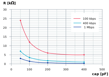
- The I2C specification allows a line capacitance of 400 pF at most.
- The value of internal pullup resistor (RPU) for nRF5340 can be found in GPIO — General purpose input/output.