Pin assignments
This section describes the pin assignment and the pin functions.
This device provides flexibility when it comes to routing and configuration of the GPIO pins. However, some pins have recommendations for how the pin should be configured or what it should be used for.
In addition to the information in the pinout tables for the respective packages, the following peripherals have dedicated pins that should be used for proper operation:
- TWI - For the fastest TWI 1 Mbps mode, the two high-speed TWI pins must be configured in the TWI peripheral's PSEL registers, and the 20 mA open drain driver enabled using the E0E1 drive setting in the DRIVE field of the PIN_CNF GPIO register.
- QSPI - For QSPI only the dedicated GPIO pins from the following table shall be used. These must be enabled using the Peripheral option of the PIN_CNF[p].MCUSEL register. The GPIO must use the high drive H0H1 configuration in the DRIVE field of the PIN_CNF GPIO register.
- SPIM4 - For the 32 Mbps SPI mode, the special purpose GPIO pins are enabled using the Peripheral option of the PIN_CNF[p].MCUSEL register. When activated, the SPIM PSEL settings are ignored, and the dedicated pins are used. The GPIO must use the high drive H0H1 configuration in the DRIVE field of the PIN_CNF GPIO register.
- TRACE - When using trace, the TRACEDATA[n] and TRACECLK GPIO pins must all use the extra high drive E0E1 configuration in the DRIVE field of the PIN_CNF GPIO register. Also, the TND option of the PIN_CNF[p].MCUSEL register must be used.
| GPIO pin | Description |
|---|---|
| P0.08 - P0.12 | Drive configuration E0E1 is available and must be used for TRACE. For 32 Mbps high-speed SPI using SPIM4, drive configuration H0H1 must be used. |
| P0.13 - P0.18 | The H0H1 drive configuration features the highest speeds of quad SPI using the direct connection of the QSPI peripheral. |
| P1.02 and P1.03 | The E0E1 drive configuration activates a 20 mA open-drain driver specifically designed for high-speed TWI. |
| Remaining pins | The E0E1 drive configuration is not supported. Using the E0E1 drive configuration will cause incorrect operation. |
For all high-speed signals, the printed circuit board (PCB) layout must ensure that connections are made using short PCB traces. Refer to the manufacturer's PCB design recommendations for additional information.
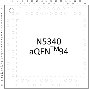
aQFN94 pin assignments
The aQFN94 package has 94 pins in addition to four corner pads and a die pad.
Some pins are named N.C. (not connected). These pins can be left unconnected, or used as recommended in the pin assignments table.
| Pin | Name | Function | Description | Recommended usage |
|---|---|---|---|---|
| A5 | VBUS | Power | 5 V input for USB 3.3 V regulator | |
| A13 | DECA | Power | Analog regulator supply decoupling | |
| A15 | DECD | Power | Digital regulator supply decoupling | |
| A17 | P1.13 | Digital I/O | General purpose I/O | |
| A19 | VDD | Power | Power supply | |
| A21 | DCC | Power | DC/DC converter output | |
| A23 | DECN | Power | Regulator supply decoupling | |
| A25 | N.C. | Connect to VSS | ||
| A27 | DECR | Power | Regulator supply decoupling | |
| B2 | D+ | USB | USB D+ | |
| B4 | D- | USB | USB D- | |
| B6 | DECUSB | Power | USB 3.3 V regulator supply decoupling | |
| B8 | VDD | Power | Power supply | |
| B10 | DCCD | Power | DC/DC converter output | |
| B12 | N.C. | Connect to VSS | ||
| B14 | P1.15 | Digital I/O | General purpose I/O | |
| B16 | P1.14 | Digital I/O | General purpose I/O | |
| B18 | P1.12 | Digital I/O | General purpose I/O | |
| B20 | P1.11 | Digital I/O | General purpose I/O | |
| B22 | P0.31 | Digital I/O | General purpose I/O | |
| B24 | P0.30 | Digital I/O | General purpose I/O | |
| B26 | N.C. | Connect to VSS | ||
| B28 | VDD | Power | Power supply | |
| B30 | XC2 | Analog input | Connection for 32 MHz crystal | |
| C1 | VDD | Power | Power supply | |
| C31 | XC1 | Analog input | Connection for 32 MHz crystal | |
| D2 | N.C. | |||
| E1 | VDDH | Power | Power supply | |
| E31 | VDD | Power | Power supply | |
| F2 | N.C. | |||
| G1 | N.C. | Connect to VSS | ||
| G31 | DECRF | Power | RADIO power supply decoupling | |
| H2 | N.C. | Connect to VSS | ||
| J1 | DCCH | Power | DC/DC converter output | |
| J31 | N.C. | Connect to VSS | ||
| K2 | N.C. | |||
| L1 | VDD | Power | Power supply | |
| L31 | ANT | RF | Single-ended antenna connection | |
| M2 | P1.00 | Digital I/O | General purpose I/O | |
| N1 | P0.00 | Digital I/O | General purpose I/O | |
| N31 | VDD | Power | Power supply | |
| P2 | P1.01 | Digital I/O | General purpose I/O | |
| R1 | P0.01 | Digital I/O | General purpose I/O | |
| R31 | P1.10 | Digital I/O | General purpose I/O | |
| T2 | N.C. | |||
| U1 | VDD | Power | Power supply | |
| U31 | P0.29 | Digital I/O | General purpose I/O | |
| V2 | P0.04 | Digital I/O | General purpose I/O | |
| W1 | P0.02 | Digital I/O | General purpose I/O | |
| W31 | SWDCLK | Debug | Serial wire debug clock input for debug and programming | |
| Y2 | P0.05 | Digital I/O | General purpose I/O | |
| AA1 | P0.03 | Digital I/O | General purpose I/O | |
| AA31 | SWDIO | Debug | Serial wire debug I/O for debug and programming | |
| AB2 | P0.06 | Digital I/O | General purpose I/O | |
| AC1 | VDD | Power | Power supply | |
| AC31 | nRESET | Reset | Pin RESET with internal pull-up resistor | |
| AD2 | P0.07 | Digital I/O | General purpose I/O | |
| AE1 | P1.02 | Digital I/O | General purpose I/O | TWI |
| AE31 | P0.28 | Digital I/O | General purpose I/O | |
| AF2 | P1.03 | Digital I/O | General purpose I/O | TWI |
| AG1 | VDD | Power | Power supply | |
| AG31 | N.C. | |||
| AH2 | P0.08 | Digital I/O | General purpose I/O | Trace, SPIM4 |
| AJ1 | P0.09 | Digital I/O | General purpose I/O | Trace, SPIM4 |
| AJ31 | VDD | Power | Power supply | |
| AK2 | P0.10 | Digital I/O | General purpose I/O | Trace, SPIM4 |
| AK4 | P0.11 | Digital I/O | General purpose I/O | Trace, SPIM4 |
| AK6 | P0.12 | Digital I/O | General purpose I/O | Trace, SPIM4 |
| AK8 | P0.14 | Digital I/O | General purpose I/O | QSPI |
| AK10 | P0.15 | Digital I/O | General purpose I/O | QSPI |
| AK12 | P0.17 | Digital I/O | General purpose I/O | QSPI |
| AK14 | P0.18 | Digital I/O | General purpose I/O | QSPI |
| AK16 | P0.20 | Digital I/O | General purpose I/O | |
| AK18 | P0.22 | Digital I/O | General purpose I/O | |
| AK20 | P0.23 | Digital I/O | General purpose I/O | |
| AK22 | P1.05 | Digital I/O | General purpose I/O | |
| AK24 | P1.07 | Digital I/O | General purpose I/O | |
| AK26 | P1.09 | Digital I/O | General purpose I/O | |
| AK28 | P0.25 | Digital I/O | General purpose I/O | |
| AK30 | P0.27 | Digital I/O | General purpose I/O | |
| AL3 | VDD | Power | Power supply | |
| AL5 | P0.13 | Digital I/O | General purpose I/O | QSPI |
| AL7 | VDD | Power | Power supply | |
| AL9 | P0.16 | Digital I/O | General purpose I/O | QSPI |
| AL11 | VDD | Power | Power supply | |
| AL13 | P0.19 | Digital I/O | General purpose I/O | |
| AL15 | P0.21 | Digital I/O | General purpose I/O | |
| AL17 | VDD | Power | Power supply | |
| AL19 | P1.04 | Digital I/O | General purpose I/O | |
| AL21 | P1.06 | Digital I/O | General purpose I/O | |
| AL23 | P1.08 | Digital I/O | General purpose I/O | |
| AL25 | VDD | Power | Power supply | |
| AL27 | P0.24 | Digital I/O | General purpose I/O | |
| AL29 | P0.26 | Digital I/O | General purpose I/O | |
| Corner pads | ||||
| A1 | N.C. | |||
| A31 | N.C. | |||
| AL1 | N.C. | |||
| AL31 | N.C. | |||
| Bottom of chip | ||||
| Die pad | VSS | Power | Ground pad. Exposed die pad must be connected to ground (VSS) for proper device operation. | |
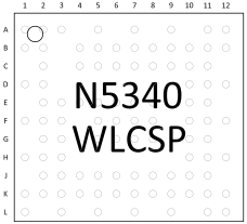
WLCSP pin assignments
This section describes the pin assignments for both the CLAA and CMAA pacakge variants.
| Pin | Name | Function | Description | Recommended usage |
|---|---|---|---|---|
| A1 | XC1 | Analog input | Connection for 32 MHz crystal | |
| A2 | XC2 | Analog input | Connection for 32 MHz crystal | |
| A3 | VDD | Power | Power supply | |
| A5 | VSS | Power | Ground | |
| A7 | DECD | Power | Regulator supply decoupling | |
| A9 | DCCD | Power | DC/DC converter output | |
| A11 | D- | USB | USB D- | |
| A12 | D+ | USB | USB D+ | |
| B1 | DECRF | Power | RADIO power supply decoupling | |
| B2 | VSS | Power | Ground | |
| B4 | DECR | Power | Regulator supply decoupling | |
| B5 | DECN | Power | Regulator supply decoupling | |
| B6 | DCC | Power | DC/DC converter output | |
| B7 | VDD | Power | Power supply | |
| B8 | DECA | Power | Regulator supply decoupling | |
| B9 | VSS | Power | Ground | |
| B10 | VDD | Power | Power supply | |
| B11 | VBUS | Power | Power | |
| B12 | VDDH | Power | Power supply | |
| C2 | VSS | Power | Ground | |
| C4 | P0.30 | Digital I/O | General purpose I/O | |
| C5 | P0.31 | Digital I/O | General purpose I/O | |
| C6 | P1.11 | Digital I/O | General purpose I/O | |
| C7 | P1.12 | Digital I/O | General purpose I/O | |
| C8 | P1.13 | Digital I/O | General purpose I/O | |
| C9 | P1.14 | Digital I/O | General purpose I/O | |
| C10 | P1.15 | Digital I/O | General purpose I/O | |
| C11 | DECUSB | Power | USB 3.3 V regulator supply decoupling | |
| D1 | ANT | RF | Single-ended antenna connection | |
| D2 | VDD | Power | Power supply | |
| D10 | P1.00 | Digital I/O | General purpose I/O | |
| D11 | DCCH | Power | DC/DC converter output | |
| D12 | VSS | Power | Ground | |
| E2 | P0.29 | Digital I/O | General purpose I/O | |
| E3 | P0.28 | Digital I/O | General purpose I/O | |
| E4 | P1.10 | Digital I/O | General purpose I/O | |
| E5 | VSS | Power | Ground | |
| E6 | VSS | Power | Ground | |
| E7 | VSS | Power | Ground | |
| E8 | VSS | Power | Ground | |
| E10 | P1.01 | Digital I/O | General purpose I/O | |
| E11 | VDD | Power | Power supply | |
| F1 | SWDIO | Debug | Serial wire debug I/O for debug and programming | |
| F2 | SWDCLK | Debug | Serial wire debug clock input for debug and programming | |
| F3 | P1.08 | Digital I/O | General purpose I/O | |
| F5 | VSS | Power | Ground | |
| F6 | VSS | Power | Ground | |
| F7 | VSS | Power | Ground | |
| F8 | VSS | Power | Ground | |
| F10 | P0.05 | Digital I/O | General purpose I/O | |
| F11 | P0.00 | Digital I/O | General purpose I/O | |
| F12 | P0.01 | Digital I/O | General purpose I/O | |
| G2 | nRESET | Reset | Pin RESET with internal pull-up resistor | |
| G3 | P1.07 | Digital I/O | General purpose I/O | |
| G5 | AVSS | Power | Ground | |
| G6 | VSS | Power | Ground | |
| G7 | VSS | Power | Ground | |
| G8 | VSS | Power | Ground | |
| G10 | P0.04 | Digital I/O | General purpose I/O | |
| G11 | P0.02 | Digital I/O | General purpose I/O | |
| H1 | P0.27 | Digital I/O | General purpose I/O | |
| H2 | P1.09 | Digital I/O | General purpose I/O | |
| H3 | P0.23 | Digital I/O | General purpose I/O | |
| H10 | P0.06 | Digital I/O | General purpose I/O | |
| H11 | VDD | Power | Power supply | |
| H12 | P0.03 | Digital I/O | General purpose I/O | |
| J2 | P0.26 | Digital I/O | General purpose I/O | |
| J3 | P1.06 | Digital I/O | General purpose I/O | |
| J4 | P0.21 | Digital I/O | General purpose I/O | |
| J5 | P0.19 | Digital I/O | General purpose I/O | |
| J6 | P0.12 | Digital I/O | General purpose I/O | |
| J7 | P0.11 | Digital I/O | General purpose I/O | Trace, SPIM4 |
| J8 | P0.10 | Digital I/O | General purpose I/O | Trace, SPIM4 |
| J9 | P0.09 | Digital I/O | General purpose I/O | Trace, SPIM4 |
| J10 | P0.07 | Digital I/O | General purpose I/O | |
| J11 | P1.02 | Digital I/O | General purpose I/O | TWI |
| K1 | VDD | Power | Power supply | |
| K2 | P0.24 | Digital I/O | General purpose I/O | |
| K3 | P1.04 | Digital I/O | General purpose I/O | |
| K4 | P0.22 | Digital I/O | General purpose I/O | |
| K5 | P0.20 | Digital I/O | General purpose I/O | |
| K6 | AVSS | Power | Ground | |
| K7 | P0.18 | Digital I/O | General purpose I/O | QSPI |
| K8 | P0.16 | Digital I/O | General purpose I/O | QSPI |
| K9 | P0.14 | Digital I/O | General purpose I/O | QSPI |
| K10 | P0.13 | Digital I/O | General purpose I/O | QSPI |
| K11 | AVSS | Power | Ground | |
| K12 | P1.03 | Digital I/O | General purpose I/O | TWI |
| L1 | P0.25 | Digital I/O | General purpose I/O | |
| L3 | P1.05 | Digital I/O | General purpose I/O | |
| L5 | VDD | Power | Power supply | |
| L7 | P0.17 | Digital I/O | General purpose I/O | QSPI |
| L9 | P0.15 | Digital I/O | General purpose I/O | QSPI |
| L11 | VDD | Power | Power supply | |
| L12 | P0.08 | Digital I/O | General purpose I/O | Trace, SPIM4 |