Reference circuitry
To ensure good RF performance when designing PCBs, it is highly recommended to use the PCB layouts and component values provided by Nordic Semiconductor.
Documentation for the different package reference circuits, including Altium Designer files, PCB layout files, and PCB production files can be downloaded from www.nordicsemi.com.
In this section, there are reference circuits for QKAA aQFN™94, CLAA WLCSP, and CMAA WLCSP, showing the components and component values to support on-chip features in a design.
- External supply from VDD is only available when power is supplied to VDDH.
- When supplying power from a USB source only, VBUS pin must be connected to VDDH pin if USB is to be used.
- Components required for DC/DC function are only needed if DC/DC mode is enabled for that regulator.
- NFC can be used in any configuration.
- USB can be used in any configuration as long as VBUS is supplied by the USB host.
- The schematics include an optional, but recommended, series resistor on the USB supply for improved immunity to transient over-voltage during VBUS connection.
| Config no. | Supply configuration | Enabled features | |||||
|---|---|---|---|---|---|---|---|
| VDDH | VDD | EXTSUPPLY | DCDC on VREGH | DCDC on VREGMAIN and VREGRADIO | USB | NFC | |
| Config. 1 | Battery/Ext. regulator | N/A | Yes | Yes | Yes | Yes | No |
| Config. 2 | N/A | Battery/Ext. regulator | No | No | Yes | Yes | Yes |
| Config. 3 | N/A | Battery/Ext. regulator | No | No | Yes | No | No |
| Config. 4 | USB (VDDH = VBUS) | N/A | No | No | No | Yes | No |
| Config no. | Supply configuration | Enabled features | |||||
|---|---|---|---|---|---|---|---|
| VDDH | VDD | EXTSUPPLY | DCDC on VREGH | DCDC on VREGMAIN and VREGRADIO | USB | NFC | |
| Config. 1 | Battery/Ext. regulator | N/A | Yes | Yes | Yes | Yes | No |
| Config. 2 | N/A | Battery/Ext. regulator | No | No | Yes | Yes | Yes |
| Config. 3 | N/A | Battery/Ext. regulator | No | No | Yes | No | No |
| Config. 4 | USB (VDDH = VBUS) | N/A | No | No | No | Yes | No |
| Config no. | Supply configuration | Enabled features | |||||
|---|---|---|---|---|---|---|---|
| VDDH | VDD | EXTSUPPLY | DCDC on VREGH | DCDC on VREGMAIN and VREGRADIO | USB | NFC | |
| Config. 1 | Battery/Ext. regulator | N/A | Yes | Yes | Yes | Yes | No |
| Config. 2 | N/A | Battery/Ext. regulator | No | No | Yes | Yes | Yes |
| Config. 3 | N/A | Battery/Ext. regulator | No | No | Yes | No | No |
| Config. 4 | USB (VDDH = VBUS) | N/A | No | No | No | Yes | No |
Circuit configuration no. 1 for QKAA aQFN94
Circuit configuration number 1 for QKAA aQFN™94 is showing the schematic and the bill of materials table.
| Config no. | Supply configuration | Enabled features | |||||
|---|---|---|---|---|---|---|---|
| VDDH | VDD | EXTSUPPLY | DCDC on VREGH | DCDC on VREGMAIN and VREGRADIO | USB | NFC | |
| Config. 1 | Battery/Ext. regulator | N/A | Yes | Yes | Yes | Yes | No |
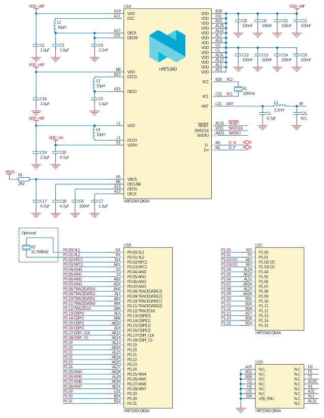
| Designator | Value | Description | Footprint |
|---|---|---|---|
| C1 | 0.7 pF | Capacitor, NP0, ±0.05 pF | 0201 |
| C2, C3, C5, C7, C16 | 1.0 µF | Capacitor, X7S, ±10% | 0402 |
| C4 | 2.2 nF | Capacitor, X7R, ±10% | 0201 |
| C6, C8, C9, C10, C11, C12, C13, C14, C15 | 100 nF | Capacitor, X7S, ±10% | 0201 |
| C17, C20 | 4.7 µF | Capacitor, X7S, ±10% | 0603 |
| C18 | 4.7 µF | Capacitor, X7R, ±10% | 0603 |
| C19 | 2.2 µF | Capacitor, X7R, ±10% | 0603 |
| C21 | N.C. | Not mounted | 0201 |
| L1 | 2.2 nH | High frequency chip inductor, ±5% | 0201 |
| L2, L3 | 10 µH | Inductor, 50 mA, ±20% | 0603 |
| L4 | 10 µH | Inductor, 80 mA, ±20% | 0603 |
| R1 | 2.2 Ω | Resistor, ±1%, 0.05 W | 0201 |
| U1 | nRF5340-QKAA | Multiprotocol Bluetooth® Low Energy, IEEE 802.15.4, ANT, and 2.4GHz proprietary System on Chip | AQFN-94 |
| X1 | 32 MHz | Crystal SMD 2016, 32 MHz, Cl=8 pF, Total Tol: ±30 ppm. For frequency tolerance requirements, see 32 MHz crystal oscillator (HFXO). | XTAL_2016 |
| X2 | 32.768 kHz | Crystal SMD 2012, 32.768 kHz, Cl=9 pF, Total Tol: ±50 ppm | XTAL_2012 |
Circuit configuration no. 2 for QKAA aQFN94
Circuit configuration number 2 for QKAA aQFN™94 is showing the schematic and the bill of materials table.
| Config no. | Supply configuration | Enabled features | |||||
|---|---|---|---|---|---|---|---|
| VDDH | VDD | EXTSUPPLY | DCDC on VREGH | DCDC on VREGMAIN and VREGRADIO | USB | NFC | |
| Config. 2 | N/A | Battery/Ext. regulator | No | No | Yes | Yes | Yes |
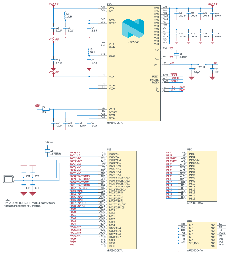
| Designator | Value | Description | Footprint |
|---|---|---|---|
| C1 | 0.7 pF | Capacitor, NP0, ±0.05 pF | 0201 |
| C2, C3, C5, C7, C16 | 1.0 µF | Capacitor, X7S, ±10% | 0402 |
| C4 | 2.2 nF | Capacitor, X7R, ±10% | 0201 |
| C6, C8, C9, C10, C11, C12, C13, C14, C15 | 100 nF | Capacitor, X7S, ±10% | 0201 |
| C17 | 4.7 µF | Capacitor, X7S, ±10% | 0603 |
| C18 | 4.7 µF | Capacitor, X7R, ±10% | 0603 |
| C21 | N.C. | Not mounted | 0201 |
| CT1, CT2, CT3, CT4 | Antenna dependent | Capacitor, NP0, ±5% | 0201 |
| L1 | 2.2 nH | High frequency chip inductor, ±5% | 0201 |
| L2, L3 | 10 µH | Inductor, 50 mA, ±20% | 0603 |
| R1 | 2.2 Ω | Resistor, ±1%, 0.05 W | 0201 |
| U1 | nRF5340-QKAA | Multiprotocol Bluetooth Low Energy, IEEE 802.15.4, ANT, and 2.4GHz proprietary System on Chip | AQFN-94 |
| X1 | 32 MHz | Crystal SMD 2016, 32 MHz, Cl=8 pF, Total Tol: ±30 ppm. For frequency tolerance requirements, see 32 MHz crystal oscillator (HFXO). | XTAL_2016 |
| X2 | 32.768 kHz | Crystal SMD 2012, 32.768 kHz, Cl=9 pF, Total Tol: ±50 ppm | XTAL_2012 |
Circuit configuration no. 3 for QKAA aQFN94
Circuit configuration number 3 for QKAA aQFN™94 is showing the schematic and the bill of materials table.
| Config no. | Supply configuration | Enabled features | |||||
|---|---|---|---|---|---|---|---|
| VDDH | VDD | EXTSUPPLY | DCDC on VREGH | DCDC on VREGMAIN and VREGRADIO | USB | NFC | |
| Config. 3 | N/A | Battery/Ext. regulator | No | No | Yes | No | No |
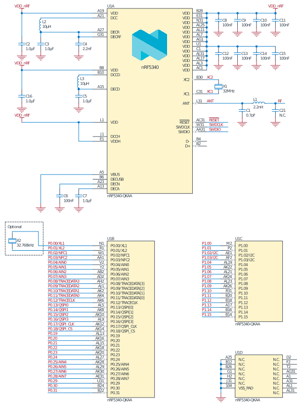
| Designator | Value | Description | Footprint |
|---|---|---|---|
| C1 | 0.7 pF | Capacitor, NP0, ±0.05 pF | 0201 |
| C2, C3, C5, C7, C16 | 1.0 µF | Capacitor, X7S, ±10% | 0402 |
| C4 | 2.2 nF | Capacitor, X7R, ±10% | 0201 |
| C6, C8, C9, C10, C11, C12, C13, C14, C15 | 100 nF | Capacitor, X7S, ±10% | 0201 |
| C21 | N.C. | Not mounted | 0201 |
| L1 | 2.2 nH | High frequency chip inductor, ±5% | 0201 |
| L2, L3 | 10 µH | Inductor, 50 mA, ±20% | 0603 |
| U1 | nRF5340-QKAA | Multiprotocol Bluetooth Low Energy, IEEE 802.15.4, ANT, and 2.4GHz proprietary System on Chip | AQFN-94 |
| X1 | 32 MHz | Crystal SMD 2016, 32 MHz, Cl=8 pF, Total Tol: ±30 ppm. For frequency tolerance requirements, see 32 MHz crystal oscillator (HFXO). | XTAL_2016 |
| X2 | 32.768 kHz | Crystal SMD 2012, 32.768 kHz, Cl=9 pF, Total Tol: ±50 ppm | XTAL_2012 |
Circuit configuration no. 4 for QKAA aQFN94
Circuit configuration number 4 for QKAA aQFN™94 is showing the schematic and the bill of materials table.
| Config no. | Supply configuration | Enabled features | |||||
|---|---|---|---|---|---|---|---|
| VDDH | VDD | EXTSUPPLY | DCDC on VREGH | DCDC on VREGMAIN and VREGRADIO | USB | NFC | |
| Config. 4 | USB (VDDH = VBUS) | N/A | No | No | No | Yes | No |
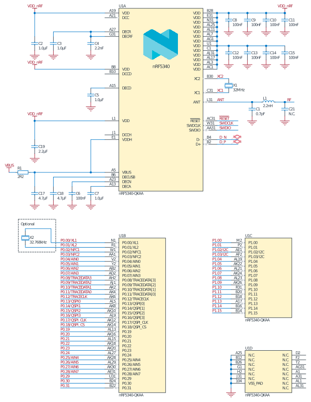
| Designator | Value | Description | Footprint |
|---|---|---|---|
| C1 | 0.7 pF | Capacitor, NP0, ±0.05 pF | 0201 |
| C2, C3, C5, C7 | 1.0 µF | Capacitor, X7S, ±10% | 0402 |
| C4 | 2.2 nF | Capacitor, X7R, ±10% | 0201 |
| C6, C8, C9, C10, C11, C12, C13, C14, C15 | 100 nF | Capacitor, X7S, ±10% | 0201 |
| C17 | 4.7 µF | Capacitor, X7S, ±10% | 0603 |
| C18 | 4.7 µF | Capacitor, X7R, ±10% | 0603 |
| C19 | 2.2 µF | Capacitor, X7R, ±10% | 0603 |
| C21 | N.C. | Not mounted | 0201 |
| L1 | 2.2 nH | High frequency chip inductor, ±5% | 0201 |
| R1 | 2.2 Ω | Resistor, ±1%, 0.05 W | 0201 |
| U1 | nRF5340-QKAA | Multiprotocol Bluetooth Low Energy, IEEE 802.15.4, ANT, and 2.4GHz proprietary System on Chip | AQFN-94 |
| X1 | 32 MHz | Crystal SMD 2016, 32 MHz, Cl=8 pF, Total Tol: ±30 ppm. For frequency tolerance requirements, see 32 MHz crystal oscillator (HFXO). | XTAL_2016 |
| X2 | 32.768 kHz | Crystal SMD 2012, 32.768 kHz, Cl=9 pF, Total Tol: ±50 ppm | XTAL_2012 |
Circuit configuration no. 1 for CLAA WLCSP
Circuit configuration number 1 for CLAA WLCSP is showing the schematic and the bill of materials table.
| Config no. | Supply configuration | Enabled features | |||||
|---|---|---|---|---|---|---|---|
| VDDH | VDD | EXTSUPPLY | DCDC on VREGH | DCDC on VREGMAIN and VREGRADIO | USB | NFC | |
| Config. 1 | Battery/Ext. regulator | N/A | Yes | Yes | Yes | Yes | No |
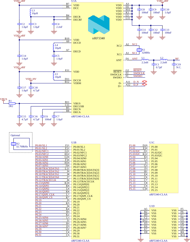
| Designator | Value | Description | Footprint |
|---|---|---|---|
| C1 | 0.7 pF | Capacitor, NP0, ±0.05 pF | 0201 |
| C2, C3, C5, C7, C10, C14, C17 | 1.0 µF | Capacitor, X7S, ±10% | 0402 |
| C4 | 2.2 nF | Capacitor, X7R, ±10% | 0201 |
| C6, C8, C9, C11, C12, C13 | 100 nF | Capacitor, X7S, ±10% | 0201 |
| C15, C18 | 4.7 µF | Capacitor, X7S, ±10% | 0603 |
| C16 | 4.7 µF | Capacitor, X7R, ±10% | 0603 |
| C19 | N.C. | Not mounted | 0201 |
| L1, L2 | 2.2 nH | High frequency chip inductor, ±5% | 0201 |
| L3, L4 | 10 µH | Inductor, 50 mA, ±20% | 0603 |
| L5 | 10 µH | Inductor, 80 mA, ±20% | 0603 |
| R1 | 2.2 Ω | Resistor, ±1%, 0.05 W | 0201 |
| U1 | nRF5340-CLAA | Multiprotocol Bluetooth Low Energy, IEEE 802.15.4, ANT, and 2.4GHz proprietary System on Chip | WLCSP-95 |
| X1 | 32 MHz | Crystal SMD 2016, 32 MHz, Cl=8 pF, Total Tol: ±30 ppm. For frequency tolerance requirements, see 32 MHz crystal oscillator (HFXO). | XTAL_2016 |
| X2 | 32.768 kHz | Crystal SMD 2012, 32.768 kHz, Cl=9 pF, Total Tol: ±50 ppm | XTAL_2012 |
Circuit configuration no. 2 for CLAA WLCSP
Circuit configuration number 2 for CLAA WLCSP is showing the schematic and the bill of materials table.
| Config no. | Supply configuration | Enabled features | |||||
|---|---|---|---|---|---|---|---|
| VDDH | VDD | EXTSUPPLY | DCDC on VREGH | DCDC on VREGMAIN and VREGRADIO | USB | NFC | |
| Config. 2 | N/A | Battery/Ext. regulator | No | No | Yes | Yes | Yes |
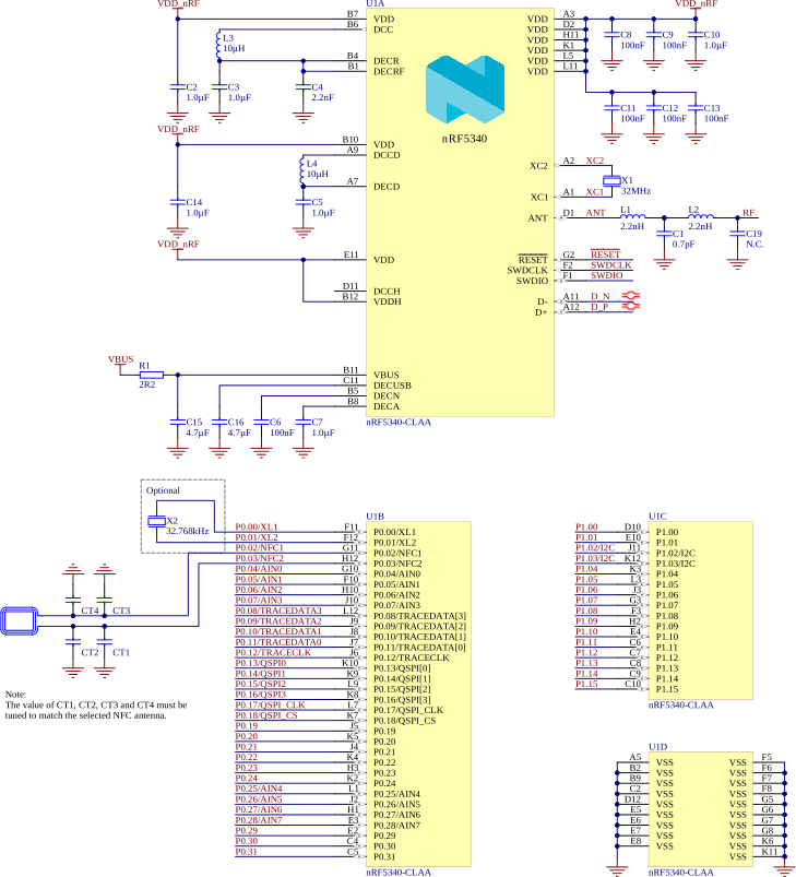
| Designator | Value | Description | Footprint |
|---|---|---|---|
| C1 | 0.7 pF | Capacitor, NP0, ±0.05 pF | 0201 |
| C2, C3, C5, C7, C10, C14 | 1.0 µF | Capacitor, X7S, ±10% | 0402 |
| C4 | 2.2 nF | Capacitor, X7R, ±10% | 0201 |
| C6, C8, C9, C11, C12, C13 | 100 nF | Capacitor, X7S, ±10% | 0201 |
| C15 | 4.7 µF | Capacitor, X7S, ±10% | 0603 |
| C16 | 4.7 µF | Capacitor, X7R, ±10% | 0603 |
| C19 | N.C. | Not mounted | 0201 |
| CT1, CT2, CT3, CT4 | Antenna dependent | Capacitor, NP0, ±5% | 0201 |
| L1, L2 | 2.2 nH | High frequency chip inductor, ±5% | 0201 |
| L3, L4 | 10 µH | Inductor, 50 mA, ±20% | 0603 |
| R1 | 2.2 Ω | Resistor, ±1%, 0.05 W | 0201 |
| U1 | nRF5340-CLAA | Multiprotocol Bluetooth Low Energy, IEEE 802.15.4, ANT, and 2.4GHz proprietary System on Chip | WLCSP-95 |
| X1 | 32 MHz | Crystal SMD 2016, 32 MHz, Cl=8 pF, Total Tol: ±30 ppm. For frequency tolerance requirements, see 32 MHz crystal oscillator (HFXO). | XTAL_2016 |
| X2 | 32.768 kHz | Crystal SMD 2012, 32.768 kHz, Cl=9 pF, Total Tol: ±50 ppm | XTAL_2012 |
Circuit configuration no. 3 for CLAA WLCSP
Circuit configuration number 3 for CLAA WLCSP is showing the schematic and the bill of materials table.
| Config no. | Supply configuration | Enabled features | |||||
|---|---|---|---|---|---|---|---|
| VDDH | VDD | EXTSUPPLY | DCDC on VREGH | DCDC on VREGMAIN and VREGRADIO | USB | NFC | |
| Config. 3 | N/A | Battery/Ext. regulator | No | No | Yes | No | No |
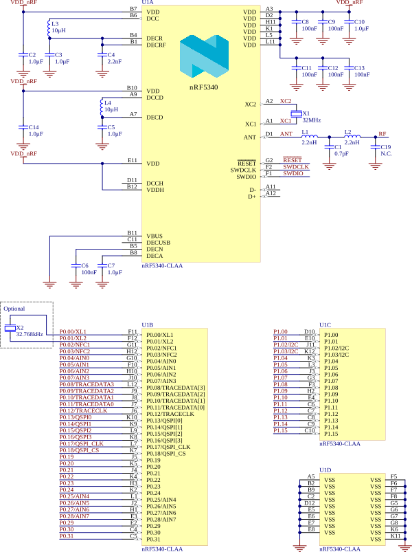
| Designator | Value | Description | Footprint |
|---|---|---|---|
| C1 | 0.7 pF | Capacitor, NP0, ±0.05 pF | 0201 |
| C2, C3, C5, C7, C10, C14 | 1.0 µF | Capacitor, X7S, ±10% | 0402 |
| C4 | 2.2 nF | Capacitor, X7R, ±10% | 0201 |
| C6, C8, C9, C11, C12, C13 | 100 nF | Capacitor, X7S, ±10% | 0201 |
| C19 | N.C. | Not mounted | 0201 |
| L1, L2 | 2.2 nH | High frequency chip inductor, ±5% | 0201 |
| L3, L4 | 10 µH | Inductor, 50 mA, ±20% | 0603 |
| U1 | nRF5340-CLAA | Multiprotocol Bluetooth Low Energy, IEEE 802.15.4, ANT, and 2.4GHz proprietary System on Chip | WLCSP-95 |
| X1 | 32 MHz | Crystal SMD 2016, 32 MHz, Cl=8 pF, Total Tol: ±30 ppm. For frequency tolerance requirements, see 32 MHz crystal oscillator (HFXO). | XTAL_2016 |
| X2 | 32.768 kHz | Crystal SMD 2012, 32.768 kHz, Cl=9 pF, Total Tol: ±50 ppm | XTAL_2012 |
Circuit configuration no. 4 for CLAA WLCSP
Circuit configuration number 4 for CLAA WLCSP is showing the schematic and the bill of materials table.
| Config no. | Supply configuration | Enabled features | |||||
|---|---|---|---|---|---|---|---|
| VDDH | VDD | EXTSUPPLY | DCDC on VREGH | DCDC on VREGMAIN and VREGRADIO | USB | NFC | |
| Config. 4 | USB (VDDH = VBUS) | N/A | No | No | No | Yes | No |
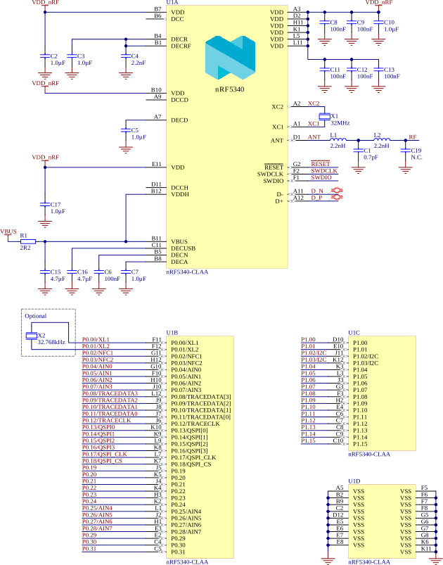
| Designator | Value | Description | Footprint |
|---|---|---|---|
| C1 | 0.7 pF | Capacitor, NP0, ±0.05 pF | 0201 |
| C2, C3, C5, C7, C10, C17 | 1.0 µF | Capacitor, X7S, ±10% | 0402 |
| C4 | 2.2 nF | Capacitor, X7R, ±10% | 0201 |
| C6, C8, C9, C11, C12, C13 | 100 nF | Capacitor, X7S, ±10% | 0201 |
| C15 | 4.7 µF | Capacitor, X7S, ±10% | 0603 |
| C16 | 4.7 µF | Capacitor, X7R, ±10% | 0603 |
| C19 | N.C. | Not mounted | 0201 |
| L1, L2 | 2.2 nH | High frequency chip inductor, ±5% | 0201 |
| R1 | 2.2 Ω | Resistor, ±1%, 0.05 W | 0201 |
| U1 | nRF5340-CLAA | Multiprotocol Bluetooth Low Energy, IEEE 802.15.4, ANT, and 2.4GHz proprietary System on Chip | WLCSP-95 |
| X1 | 32 MHz | Crystal SMD 2016, 32 MHz, Cl=8 pF, Total Tol: ±30 ppm. For frequency tolerance requirements, see 32 MHz crystal oscillator (HFXO). | XTAL_2016 |
| X2 | 32.768 kHz | Crystal SMD 2012, 32.768 kHz, Cl=9 pF, Total Tol: ±50 ppm | XTAL_2012 |
Circuit configuration no. 1 for CMAA WLCSP
Circuit configuration number 1 for CMAA WLCSP is showing the schematic and the bill of materials table.
| Config no. | Supply configuration | Enabled features | |||||
|---|---|---|---|---|---|---|---|
| VDDH | VDD | EXTSUPPLY | DCDC on VREGH | DCDC on VREGMAIN and VREGRADIO | USB | NFC | |
| Config. 1 | Battery/Ext. regulator | N/A | Yes | Yes | Yes | Yes | No |
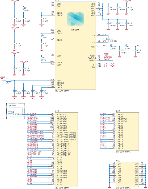
| Designator | Value | Description | Footprint |
|---|---|---|---|
| C1 | 0.7 pF | Capacitor, NP0, ±0.05 pF | 0201 |
| C2, C3, C5, C7, C10, C14, C17 | 1.0 µF | Capacitor, X7S, ±10% | 0402 |
| C4 | 2.2 nF | Capacitor, X7R, ±10% | 0201 |
| C6, C8, C9, C11, C12, C13 | 100 nF | Capacitor, X7S, ±10% | 0201 |
| C15, C18 | 4.7 µF | Capacitor, X7S, ±10% | 0603 |
| C16 | 4.7 µF | Capacitor, X7R, ±10% | 0603 |
| C19 | N.C. | Not mounted | 0201 |
| L1, L2 | 2.2 nH | High frequency chip inductor, ±5% | 0201 |
| L3, L4 | 10 µH | Inductor, 50 mA, ±20% | 0603 |
| L5 | 10 µH | Inductor, 80 mA, ±20% | 0603 |
| R1 | 2.2 Ω | Resistor, ±1%, 0.05 W | 0201 |
| U1 | nRF5340-CMAA | Multiprotocol Bluetooth Low Energy, IEEE 802.15.4, ANT, and 2.4GHz proprietary System on Chip | WLCSP-95 |
| X1 | 32 MHz | Crystal SMD 2016, 32 MHz, Cl=8 pF, Total Tol: ±30 ppm. For frequency tolerance requirements, see 32 MHz crystal oscillator (HFXO). | XTAL_2016 |
| X2 | 32.768 kHz | Crystal SMD 2012, 32.768 kHz, Cl=9 pF, Total Tol: ±50 ppm | XTAL_2012 |
Circuit configuration no. 2 for CMAA WLCSP
Circuit configuration number 2 for CMAA WLCSP is showing the schematic and the bill of materials table.
| Config no. | Supply configuration | Enabled features | |||||
|---|---|---|---|---|---|---|---|
| VDDH | VDD | EXTSUPPLY | DCDC on VREGH | DCDC on VREGMAIN and VREGRADIO | USB | NFC | |
| Config. 2 | N/A | Battery/Ext. regulator | No | No | Yes | Yes | Yes |
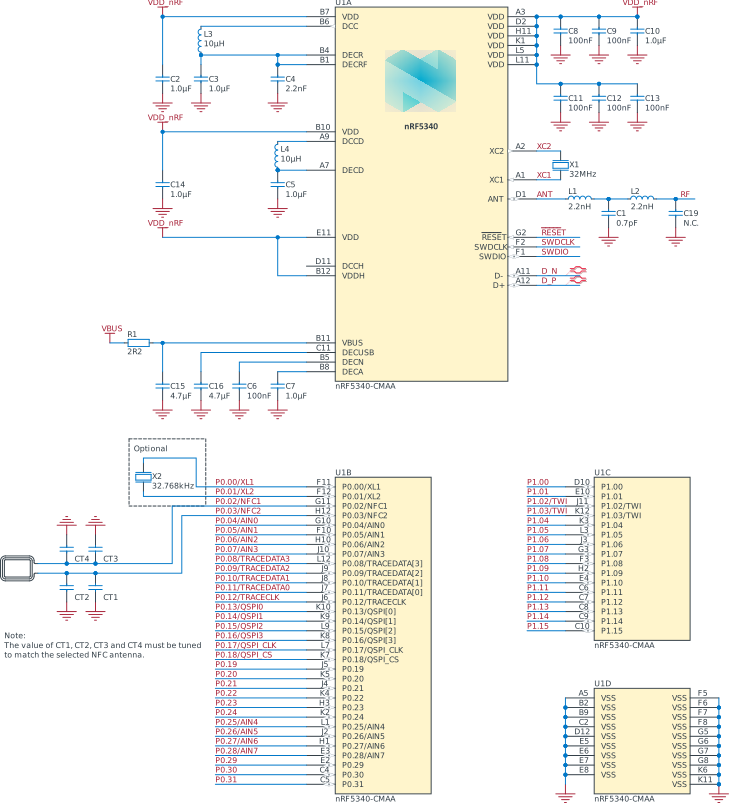
| Designator | Value | Description | Footprint |
|---|---|---|---|
| C1 | 0.7 pF | Capacitor, NP0, ±0.05 pF | 0201 |
| C2, C3, C5, C7, C10, C14 | 1.0 µF | Capacitor, X7S, ±10% | 0402 |
| C4 | 2.2 nF | Capacitor, X7R, ±10% | 0201 |
| C6, C8, C9, C11, C12, C13 | 100 nF | Capacitor, X7S, ±10% | 0201 |
| C15 | 4.7 µF | Capacitor, X7S, ±10% | 0603 |
| C16 | 4.7 µF | Capacitor, X7R, ±10% | 0603 |
| C19 | N.C. | Not mounted | 0201 |
| CT1, CT2, CT3, CT4 | Antenna dependent | Capacitor, NP0, ±5% | 0201 |
| L1, L2 | 2.2 nH | High frequency chip inductor, ±5% | 0201 |
| L3, L4 | 10 µH | Inductor, 50 mA, ±20% | 0603 |
| R1 | 2.2 Ω | Resistor, ±1%, 0.05 W | 0201 |
| U1 | nRF5340-CMAA | Multiprotocol Bluetooth Low Energy, IEEE 802.15.4, ANT, and 2.4GHz proprietary System on Chip | WLCSP-95 |
| X1 | 32 MHz | Crystal SMD 2016, 32 MHz, Cl=8 pF, Total Tol: ±30 ppm. For frequency tolerance requirements, see 32 MHz crystal oscillator (HFXO). | XTAL_2016 |
| X2 | 32.768 kHz | Crystal SMD 2012, 32.768 kHz, Cl=9 pF, Total Tol: ±50 ppm | XTAL_2012 |
Circuit configuration no. 3 for CMAA WLCSP
Circuit configuration number 3 for CMAA WLCSP is showing the schematic and the bill of materials table.
| Config no. | Supply configuration | Enabled features | |||||
|---|---|---|---|---|---|---|---|
| VDDH | VDD | EXTSUPPLY | DCDC on VREGH | DCDC on VREGMAIN and VREGRADIO | USB | NFC | |
| Config. 3 | N/A | Battery/Ext. regulator | No | No | Yes | No | No |
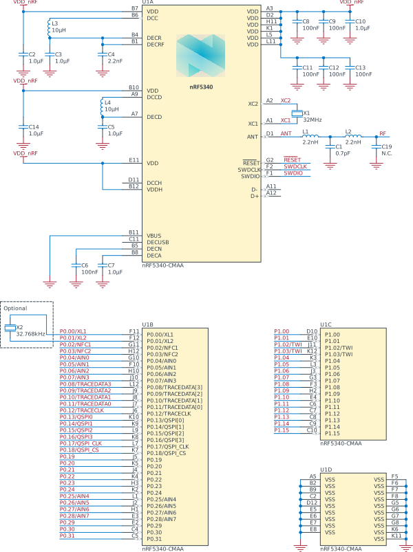
| Designator | Value | Description | Footprint |
|---|---|---|---|
| C1 | 0.7 pF | Capacitor, NP0, ±0.05 pF | 0201 |
| C2, C3, C5, C7, C10, C14 | 1.0 µF | Capacitor, X7S, ±10% | 0402 |
| C4 | 2.2 nF | Capacitor, X7R, ±10% | 0201 |
| C6, C8, C9, C11, C12, C13 | 100 nF | Capacitor, X7S, ±10% | 0201 |
| C19 | N.C. | Not mounted | 0201 |
| L1, L2 | 2.2 nH | High frequency chip inductor, ±5% | 0201 |
| L3, L4 | 10 µH | Inductor, 50 mA, ±20% | 0603 |
| U1 | nRF5340-CMAA | Multiprotocol Bluetooth Low Energy, IEEE 802.15.4, ANT, and 2.4GHz proprietary System on Chip | WLCSP-95 |
| X1 | 32 MHz | Crystal SMD 2016, 32 MHz, Cl=8 pF, Total Tol: ±30 ppm. For frequency tolerance requirements, see 32 MHz crystal oscillator (HFXO). | XTAL_2016 |
| X2 | 32.768 kHz | Crystal SMD 2012, 32.768 kHz, Cl=9 pF, Total Tol: ±50 ppm | XTAL_2012 |
Circuit configuration no. 4 for CMAA WLCSP
Circuit configuration number 4 for CMAA WLCSP is showing the schematic and the bill of materials table.
| Config no. | Supply configuration | Enabled features | |||||
|---|---|---|---|---|---|---|---|
| VDDH | VDD | EXTSUPPLY | DCDC on VREGH | DCDC on VREGMAIN and VREGRADIO | USB | NFC | |
| Config. 4 | USB (VDDH = VBUS) | N/A | No | No | No | Yes | No |
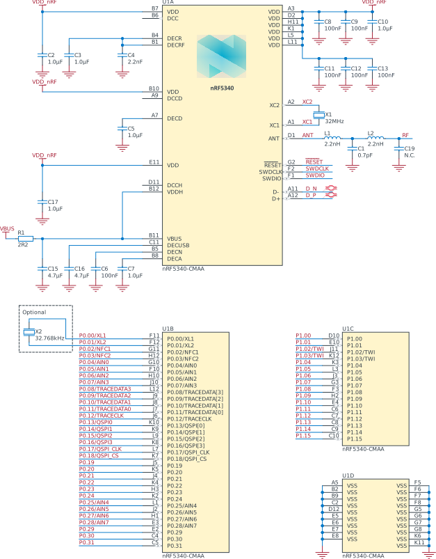
| Designator | Value | Description | Footprint |
|---|---|---|---|
| C1 | 0.7 pF | Capacitor, NP0, ±0.05 pF | 0201 |
| C2, C3, C5, C7, C10, C17 | 1.0 µF | Capacitor, X7S, ±10% | 0402 |
| C4 | 2.2 nF | Capacitor, X7R, ±10% | 0201 |
| C6, C8, C9, C11, C12, C13 | 100 nF | Capacitor, X7S, ±10% | 0201 |
| C15 | 4.7 µF | Capacitor, X7S, ±10% | 0603 |
| C16 | 4.7 µF | Capacitor, X7R, ±10% | 0603 |
| C19 | N.C. | Not mounted | 0201 |
| L1, L2 | 2.2 nH | High frequency chip inductor, ±5% | 0201 |
| R1 | 2.2 Ω | Resistor, ±1%, 0.05 W | 0201 |
| U1 | nRF5340-CMAA | Multiprotocol Bluetooth Low Energy, IEEE 802.15.4, ANT, and 2.4GHz proprietary System on Chip | WLCSP-95 |
| X1 | 32 MHz | Crystal SMD 2016, 32 MHz, Cl=8 pF, Total Tol: ±30 ppm. For frequency tolerance requirements, see 32 MHz crystal oscillator (HFXO). | XTAL_2016 |
| X2 | 32.768 kHz | Crystal SMD 2012, 32.768 kHz, Cl=9 pF, Total Tol: ±50 ppm | XTAL_2012 |
PCB layout example
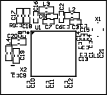
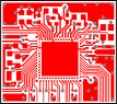
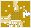
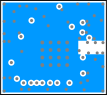
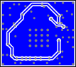
The PCB layout in the following figure is a reference layout for Circuit configuration no. 1 for QKAA aQFN™94.
For all available reference layouts, see the product page for nRF5340 on www.nordicsemi.com.
PMIC support
The nRF53 Series is comprehensively supported by Nordic Semiconductor's own range of PMICs (Power Management Integrated Circuits). These PMICs are meticulously designed to enhance the performance and efficiency of the nRF53 Series devices. This integration ensures the longest battery life and the highest reliability for the end application. The synergy between the nRF53 Series and the Nordic PMICs highlights Nordic Semiconductor's commitment to providing a complete and cohesive solution for their customers' needs in wireless technology applications.