OSCILLATORS — Oscillator control
The system oscillators are automatically controlled by the clock control system, see CLOCK — Clock control.
- High-frequency 32 MHz crystal oscillator (HFXO)
- Low-frequency 32.768 kHz crystal oscillator (LFXO)
The crystal oscillators can be configured to use either internal or external capacitors.
High-frequency (32 MHz) crystal oscillator (HFXO)
The high-frequency crystal oscillator (HFXO) is controlled by a 32 MHz external crystal.
The crystal oscillator is designed for use with an AT-cut quartz crystal in parallel resonant mode and is connected between pins XC1 and XC2. For correct oscillation frequency, the load capacitance must match the specification in the crystal datasheet. The following figure shows how the 32 MHz crystal is connected to the high frequency crystal oscillator.
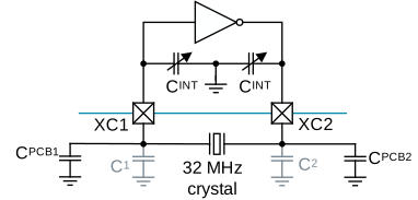
The device can be used with external capacitors C1 and C2 or the internal capacitors CINT, which are configurable.
For reliable operation, the crystal load capacitance, shunt capacitance, equivalent series resistance, and drive level must comply with the specifications in table 32 MHz crystal oscillator (HFXO). It is recommended to use a crystal with lower than maximum load capacitance and/or shunt capacitance. A low load capacitance reduces both start up time and current consumption.
When using internal capacitors, the load capacitance (CL) is the total capacitance seen by the crystal across its terminals and is calculated by the following equation.
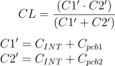
CINT is the value of the internal capacitors. Cpcb1 and Cpcb2 are stray capacitance on the PCB.
INTCAP = (((CAPACITANCE-5.5)*(FICR->XOSC32MTRIM.SLOPE+791)) +
FICR->XOSC32MTRIM.OFFSET*4)/256CAPACITANCEis the desired capacitor value of CINT in pF, holding any value between 4.0 pF and 17.0 pF in 0.25 pF steps.FICR->XOSC32MTRIMare factory trim values which vary between devices.
After HFXO starts, the device uses the internal capacitor together with the external crystal after configuration.
Using external capacitors
It is possible to use external capacitors after disabling the internal capacitor.
When using external capacitors, the load capacitance (CL) is the total capacitance seen by the crystal across its terminals. It is calculated by the following equation.
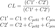
C1 and C2 are the external capacitors. Cpcb1 and Cpcb2 are stray capacitance on the PCB. Cpin is the pin input capacitance on pins XC1 and XC2.
When using external capacitors, disable the internal capacitor by setting OSCILLATORS.XOSC32M.CONFIG.INTCAP to 0.
Crystal selection
Several crystals are supported by the 32 MHz crystal oscillator.
The following figure shows a simple model of a crystal. It has R-L-C series components, called equivalent series resistance (ESR), motional capacitance (C0=N ), and motional inductance (LM ). The capacitor in parallel, C0 , is called the shunt capacitance, and models the package capacitance.
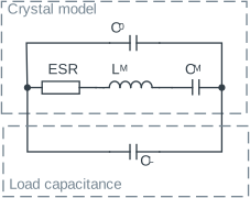
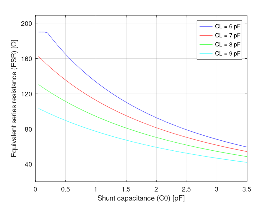
The crystal needs to have parameters ESR, C0 , and CL selected to ensure the crystal oscillator is stable.
The following figure shows the maximum allowable combinations of ESR, C0 and CL for a given crystal. A crystal is supported if that crystal's parameters fall directly on the line or below it. Crystals that are above the line are not supported.
Low-frequency (32.768 kHz) crystal oscillator (LFXO)
For clock accuracy higher than LFRC, the 32.768 kHz crystal oscillator (LFXO) must be used.
To use the LFXO, a 32.768 kHz crystal must be connected between the XL1 and XL2 pins, as shown in the following figure.
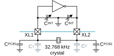
The device can be used with external capacitors C1 and C2 or the built-in configurable internal capacitors CINT.
When using internal capacitors, the load capacitance (CL) is the total capacitance seen by the crystal across its terminals. It is calculated by the following equation.
CINT is the value of the internal capacitors. Cpcb1 and Cpcb2 are stray capacitance on the PCB.
INTCAP = round( (2*CAPACITANCE - 12) * (FICR->XOSC32KTRIM.SLOPE + 0.765625 * 512)/512 + FICR->XOSC32KTRIM.OFFSET/64 )- CAPACITANCE is the desired capacitor value in pF, holding any value between 3 pF and 18 pF in 0.65 pF steps.
- FICR->XOSC32KTRIM are factory trim values which are device specific.
When LFXO starts, it will use the internal capacitor together with the external crystal.
Using external capacitors
When using external capacitors, the load capacitance (CL) is the total capacitance seen by the crystal across its terminals. It is calculated by the following equation.
C1 and C2 are ceramic SMD capacitors connected between each crystal terminal and ground. Cpcb1 and Cpcb2 are stray capacitance on the PCB. Cpin is the pin input capacitance on pins XL1 and XL2. The load capacitors C1 and C2 must have the same value.
When using external capacitors, the internal capacitor is disabled by setting OSCILLATORS.XOSC32KI.INTCAP to 0.
External source
The 32.768 kHz crystal oscillator (LFXO) is designed to work with external sources.
The device can use a rail-to-rail clock, where the signal should be applied to the XL1 pin with the XL2 pin left unconnected. To enable rail-to-rail clock, set XOSC32KI.BYPASS=Enabled.
Using an external source requires that CLOCK.LFCLK.SRC=LFXO.
CPU clock frequency selection
The CPU clock frequency is configurable on boot in the register PLL.FREQ (Retained).
The device supports 64 or 128 MHz frequency.
The device starts at 64 MHz. For higher frequencies, it must be configured when the CPU starts and before any peripherals that use the high-frequency clock are enabled. Changing the frequency on a running system or to an unsupported value causes undefined system behavior and the device can malfunction.
Registers
Instances
| Instance | Domain | Base address | TrustZone | Split access | Description | ||
|---|---|---|---|---|---|---|---|
| Map | Att | DMA | |||||
OSCILLATORS : S | GLOBAL | 0x50120000 | US | S | NA | No | Oscillator control |
Register overview
| Register | Offset | TZ | Description |
|---|---|---|---|
| XOSC32M.CONFIG.INTCAP | 0x71C | Crystal load capacitor as seen by the crystal across its terminals, including pin capacitance but excluding PCB stray capacitance. | |
| PLL.FREQ | 0x800 | Set speed of MCU power domain, including CPU This register is retained. | |
| PLL.CURRENTFREQ | 0x804 | Current speed of MCU power domain, including CPU This register is retained. | |
| XOSC32KI.BYPASS | 0x900 | Enable or disable bypass of LFCLK crystal oscillator with external clock source | |
| XOSC32KI.INTCAP | 0x904 | Programmable capacitance of XL1 and XL2 This register is retained. |
XOSC32M
32 MHz oscillator control
XOSC32M.CONFIG.INTCAP
Address offset: 0x71C
Crystal load capacitor as seen by the crystal across its terminals, including pin capacitance but excluding PCB stray capacitance.
| Bit number | 31 | 30 | 29 | 28 | 27 | 26 | 25 | 24 | 23 | 22 | 21 | 20 | 19 | 18 | 17 | 16 | 15 | 14 | 13 | 12 | 11 | 10 | 9 | 8 | 7 | 6 | 5 | 4 | 3 | 2 | 1 | 0 | |||
|---|---|---|---|---|---|---|---|---|---|---|---|---|---|---|---|---|---|---|---|---|---|---|---|---|---|---|---|---|---|---|---|---|---|---|---|
| ID | A | A | A | A | A | A | |||||||||||||||||||||||||||||
| Reset 0x00000020 | 0 | 0 | 0 | 0 | 0 | 0 | 0 | 0 | 0 | 0 | 0 | 0 | 0 | 0 | 0 | 0 | 0 | 0 | 0 | 0 | 0 | 0 | 0 | 0 | 0 | 0 | 1 | 0 | 0 | 0 | 0 | 0 | |||
| ID | R/W | Field | Value ID | Value | Description | ||||||||||||||||||||||||||||||
| A | RW | VAL | Crystal load capacitor value Use the provided equation in OSCILLATORS — Oscillator control to calculate the register value. | ||||||||||||||||||||||||||||||||
PLL
Oscillator control
PLL.FREQ (Retained)
Address offset: 0x800
Set speed of MCU power domain, including CPU
This register is retained.
| Bit number | 31 | 30 | 29 | 28 | 27 | 26 | 25 | 24 | 23 | 22 | 21 | 20 | 19 | 18 | 17 | 16 | 15 | 14 | 13 | 12 | 11 | 10 | 9 | 8 | 7 | 6 | 5 | 4 | 3 | 2 | 1 | 0 | |||
|---|---|---|---|---|---|---|---|---|---|---|---|---|---|---|---|---|---|---|---|---|---|---|---|---|---|---|---|---|---|---|---|---|---|---|---|
| ID | A | A | |||||||||||||||||||||||||||||||||
| Reset 0x00000003 | 0 | 0 | 0 | 0 | 0 | 0 | 0 | 0 | 0 | 0 | 0 | 0 | 0 | 0 | 0 | 0 | 0 | 0 | 0 | 0 | 0 | 0 | 0 | 0 | 0 | 0 | 0 | 0 | 0 | 0 | 1 | 1 | |||
| ID | R/W | Field | Value ID | Value | Description | ||||||||||||||||||||||||||||||
| A | RW | FREQ | Select CPU speed | ||||||||||||||||||||||||||||||||
CK128M | 1 | 128 MHz | |||||||||||||||||||||||||||||||||
CK64M | 3 | 64 MHz | |||||||||||||||||||||||||||||||||
PLL.CURRENTFREQ (Retained)
Address offset: 0x804
Current speed of MCU power domain, including CPU
This register is retained.
| Bit number | 31 | 30 | 29 | 28 | 27 | 26 | 25 | 24 | 23 | 22 | 21 | 20 | 19 | 18 | 17 | 16 | 15 | 14 | 13 | 12 | 11 | 10 | 9 | 8 | 7 | 6 | 5 | 4 | 3 | 2 | 1 | 0 | |||
|---|---|---|---|---|---|---|---|---|---|---|---|---|---|---|---|---|---|---|---|---|---|---|---|---|---|---|---|---|---|---|---|---|---|---|---|
| ID | A | A | |||||||||||||||||||||||||||||||||
| Reset 0x00000003 | 0 | 0 | 0 | 0 | 0 | 0 | 0 | 0 | 0 | 0 | 0 | 0 | 0 | 0 | 0 | 0 | 0 | 0 | 0 | 0 | 0 | 0 | 0 | 0 | 0 | 0 | 0 | 0 | 0 | 0 | 1 | 1 | |||
| ID | R/W | Field | Value ID | Value | Description | ||||||||||||||||||||||||||||||
| A | R | CURRENTFREQ | Active CPU speed | ||||||||||||||||||||||||||||||||
CK128M | 1 | 128 MHz | |||||||||||||||||||||||||||||||||
CK64M | 3 | 64 MHz | |||||||||||||||||||||||||||||||||
XOSC32KI
32.768 kHz oscillator control
XOSC32KI.BYPASS
Address offset: 0x900
Enable or disable bypass of LFCLK crystal oscillator with external clock source
| Bit number | 31 | 30 | 29 | 28 | 27 | 26 | 25 | 24 | 23 | 22 | 21 | 20 | 19 | 18 | 17 | 16 | 15 | 14 | 13 | 12 | 11 | 10 | 9 | 8 | 7 | 6 | 5 | 4 | 3 | 2 | 1 | 0 | |||
|---|---|---|---|---|---|---|---|---|---|---|---|---|---|---|---|---|---|---|---|---|---|---|---|---|---|---|---|---|---|---|---|---|---|---|---|
| ID | A | ||||||||||||||||||||||||||||||||||
| Reset 0x00000000 | 0 | 0 | 0 | 0 | 0 | 0 | 0 | 0 | 0 | 0 | 0 | 0 | 0 | 0 | 0 | 0 | 0 | 0 | 0 | 0 | 0 | 0 | 0 | 0 | 0 | 0 | 0 | 0 | 0 | 0 | 0 | 0 | |||
| ID | R/W | Field | Value ID | Value | Description | ||||||||||||||||||||||||||||||
| A | RW | BYPASS | Enable or disable bypass of LFCLK crystal oscillator with external clock source | ||||||||||||||||||||||||||||||||
Disabled | 0 | Disable (use crystal) | |||||||||||||||||||||||||||||||||
Enabled | 1 | Enable (use rail-to-rail external source) | |||||||||||||||||||||||||||||||||
XOSC32KI.INTCAP (Retained)
Address offset: 0x904
Programmable capacitance of XL1 and XL2
Use the provided equation in OSCILLATORS — Oscillator control to calculate the register value.
This register is retained.
| Bit number | 31 | 30 | 29 | 28 | 27 | 26 | 25 | 24 | 23 | 22 | 21 | 20 | 19 | 18 | 17 | 16 | 15 | 14 | 13 | 12 | 11 | 10 | 9 | 8 | 7 | 6 | 5 | 4 | 3 | 2 | 1 | 0 | |||
|---|---|---|---|---|---|---|---|---|---|---|---|---|---|---|---|---|---|---|---|---|---|---|---|---|---|---|---|---|---|---|---|---|---|---|---|
| ID | A | A | A | A | A | ||||||||||||||||||||||||||||||
| Reset 0x00000017 | 0 | 0 | 0 | 0 | 0 | 0 | 0 | 0 | 0 | 0 | 0 | 0 | 0 | 0 | 0 | 0 | 0 | 0 | 0 | 0 | 0 | 0 | 0 | 0 | 0 | 0 | 0 | 1 | 0 | 1 | 1 | 1 | |||
| ID | R/W | Field | Value ID | Value | Description | ||||||||||||||||||||||||||||||
| A | RW | VAL | Crystal load capacitor as seen by the crystal across its terminals, including pin capacitance but excluding PCB stray capacitance. Use the provided equation in "Using internal capacitors section" to calculate the register value. | ||||||||||||||||||||||||||||||||