DPPI — Distributed programmable peripheral interconnect
The distributed programmable peripheral interconnect (DPPI) enables peripherals to interact autonomously with each other through tasks and events, without CPU intervention. DPPI allows precise synchronization between peripherals when real-time application constraints exist, and eliminates the need for CPU involvement to implement behavior which can be predefined using the DPPI.
The main features of DPPI are the following:
- Peripheral tasks can subscribe to channels
- Peripheral events can be published on channels
- Publish/subscribe pattern enabling multiple connection options that include the following:
- One-to-one
- One-to-many
- Many-to-one
- Many-to-many
The DPPI consists of several PPIBus modules. These modules are connected to a fixed number of DPPI channels and a DPPI controller (DPPIC).
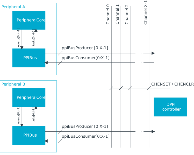
Channel publish and subscribe
The DPPI system directs peripheral events to a channel (publishing) and converts events from a channel into peripheral tasks (subscribing).
All peripherals include the following:
- One publish register per event
- One subscribe register per task
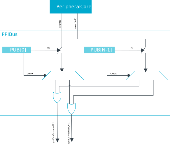
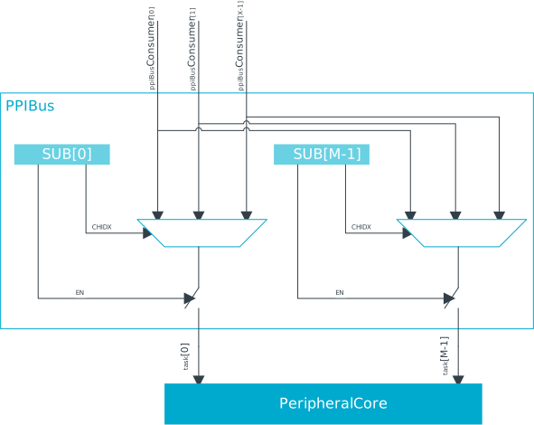
The publish and subscribe registers have two fields. A channel index field (CHIDX) determines which channel an event is published to, or which channel a task is subscribed to. In addition there is an ENABLE field that must be set to 1 to activate the operation.
Writing non-existing channel index (CHIDX) numbers into a peripheral's publish or subscribe registers will yield unexpected results.
One event can trigger multiple tasks by subscribing different tasks to the same channel. Similarly, one task can be triggered by multiple events by publishing different events to the same channel. For advanced use cases, multiple events and multiple tasks can connect to the same channel forming a many-to-many connection. If multiple events are published on the same channel at the same time, the events are merged and only one event is routed through the DPPI.
The following figure shows how peripheral events are routed onto different channels based on publish registers.
The following figure illustrates how peripheral tasks are triggered from different channels based on subscribe registers.
DPPI controller (DPPIC)
Enabling and disabling of DPPI channels is handled through DPPIC.
There are two ways of enabling or disabling a DPPI channel using DPPIC:
- Enable or disable channels individually using registers CHEN, CHENSET, and CHENCLR.
- Enable or disable channels in channel groups using the groups' tasks ENABLE and DISABLE. Channel groups should be defined via the CHG registers before these tasks are triggered.
DPPIC tasks (for example CHG[0].EN) can be triggered through DPPI like any other task, which means they can be linked to a DPPI channel through the subscribe registers.
In order to write to CHG[n], the corresponding CHG[n].EN and CHG[n].DIS subscribe registers must be disabled. Writes to CHG[n] are ignored if any of the two subscribe registers are enabled.
Connection examples
Several connection options are available with DPPI. Examples are given for how to create one-to-one and many-to-many connections.
One-to-one connection
This example shows how to create a one-to-one connection between the TIMER compare register and the SAADC start task.
The channel configuration is set up first. TIMER will publish its COMPARE0 event on channel 0, and SAADC will subscribe its START task to events on the same channel. When this is finished, the channel is enabled through the DPPIC.
NRF_TIMER20->PUBLISH_COMPARE[0] = (0 << TIMER_PUBLISH_COMPARE_CHIDX_Pos) | TIMER_PUBLISH_COMPARE_EN_Msk;
NRF_SAADC->SUBSCRIBE_START = (0 << SAADC_SUBSCRIBE_START_CHIDX_Pos) | SAADC_SUBSCRIBE_START_EN_Msk;
NRF_DPPIC20->CHENSET = DPPIC_CHENSET_CH0_Msk;
Many-to-many connection
The following example shows how to create a many-to-many connection, showcasing the DPPIC's channel group functionality.
NRF_DPPIC20->CHG[0] = (DPPIC_CHG_CH0_Included << DPPIC_CHG_CH0_Pos);
NRF_GPIOTE20->PUBLISH_IN[0] = (0 << GPIOTE_PUBLISH_IN_CHIDX_Pos) | GPIOTE_PUBLISH_IN_EN_Msk;
NRF_TIMER20->PUBLISH_COMPARE[0] = (0 << TIMER_PUBLISH_COMPARE_CHIDX_Pos) | TIMER_PUBLISH_COMPARE_EN_Msk;
NRF_SAADC->SUBSCRIBE_START = (0 << SAADC_SUBSCRIBE_START_CHIDX_Pos) | SAADC_SUBSCRIBE_START_EN_Msk;
NRF_DPPIC20->SUBSCRIBE_CHG[0].DIS = DPPIC_CHENSET_CH0_Msk | DPPIC_SUBSCRIBE_CHG_DIS_EN_Msk;
NRF_DPPIC20->TASK_CHG[0].EN = 1;
Special considerations for a system implementing TrustZone for Cortex-M processors
DPPI is implemented with split security in order to handle both secure and non-secure accesses. In a system implementing the TrustZone® for Cortex®-M technology, DPPI channels can be defined as secure or non-secure using the SPU.
A peripheral configured as non-secure can only subscribe to or publish on non-secure DPPI channels. A peripheral configured as secure can access all DPPI channels. DPPI handles both secure and non-secure accesses, but behaves differently depending on the access type.
- A non-secure peripheral access can only configure and control the DPPI channels defined as non-secure in the SPU.DPPI.PERM[n] register
- A secure peripheral access can control all the DPPI channels, independently of the SPU.DPPI.PERM[n] register
Non-secure access to a DPPI register or bit field controlling a channel marked as secure in a SPU.DPPI[n].PERM register is ignored. Write access has no effect, and read access returns a zero value.
Exceptions are not triggered when non-secure accesses target a register or a bit field
controlling a secure channel. For example, if the bit i is set in
the SPU.DPPI[0].PERM register (declaring DPPI channel [i] as secure), then the
following is true:
- Non-secure write access to registers CHEN, CHENSET, and CHENCLR cannot write bit
iof these registers - Non-secure write access to registers TASK_CHG[j].EN and TASK_CHG[j].DIS is ignored if
the channel group
jcontains at least one channel defined as secure (it can be the channel [i] itself or any channel declared as secure) - Non-secure read access to registers CHEN, CHENSET, and CHENCLR always read 0 for the
bit at position
i
For the channel configuration registers (CHG[]), access from non-secure code is only
possible if the included channels are all non-secure, whether the channels are
enabled or not. If register CHG[g] included one or more secure channels, then the
group g is considered as secure, and only secure transfers can read
to or write from CHG[g]. A non-secure write access is ignored, and a non-secure read
access returns 0.
The DPPI can subscribe to secure and non-secure channels through the SUBSCRIBE_CHG[] registers in order to trigger the task for enabling or disabling channel groups. An event from a secure channel is ignored if the group subscribing to this channel is non-secure. A secure group can subscribe to a non-secure channel or a secure channel.
Channel group
Creating a channel group allows all channels in that group to be simultaneously enabled or disabled. The security attribute for a channel group (secure or non-secure) is defined as follows:
- If all channels (enabled or not) within a group are non-secure, then the group is considered non-secure
- If at least one of the channels (enabled or not) within the group is secure, then the group is considered secure
Split security
Individual DPPI channels and channel groups can have independent security attributes.
The split security of DPPI means it handles both secure and non-secure code access. DPPI channels and channel groups can be defined as secure or non-secure.
For more information on DPPI security, see DPPIC.
Registers
Instances
| Instance | Domain | Base address | TrustZone | Split access | Description | ||
|---|---|---|---|---|---|---|---|
| Map | Att | DMA | |||||
DPPIC00 : S | GLOBAL | 0x50042000 | US | S | NA | Yes | DPPI controller DPPIC00 |
DPPIC10 : S | GLOBAL | 0x50082000 | US | S | NA | Yes | DPPI controller DPPIC10 |
DPPIC20 : S | GLOBAL | 0x500C2000 | US | S | NA | Yes | DPPI controller DPPIC20 |
DPPIC30 : S | GLOBAL | 0x50102000 | US | S | NA | Yes | DPPI controller DPPIC30 |
Configuration
| Instance | Domain | Configuration |
|---|---|---|
DPPIC00 : S | GLOBAL | 8 DPPI channels 2 DPPI groups |
DPPIC10 : S | GLOBAL | 24 DPPI channels 6 DPPI groups |
DPPIC20 : S | GLOBAL | 16 DPPI channels 6 DPPI groups |
DPPIC30 : S | GLOBAL | 4 DPPI channels 2 DPPI groups |
Register overview
| Register | Offset | TZ | Description |
|---|---|---|---|
| TASKS_CHG[n].EN | 0x000 | Enable channel group n | |
| TASKS_CHG[n].DIS | 0x004 | Disable channel group n | |
| SUBSCRIBE_CHG[n].EN | 0x080 | Subscribe configuration for task CHG[n].EN | |
| SUBSCRIBE_CHG[n].DIS | 0x084 | Subscribe configuration for task CHG[n].DIS | |
| CHEN | 0x500 | Channel enable register | |
| CHENSET | 0x504 | Channel enable set register | |
| CHENCLR | 0x508 | Channel enable clear register | |
| CHG[n] | 0x800 | Channel group n Note: Writes to this register are ignored if either SUBSCRIBE_CHG[n].EN or SUBSCRIBE_CHG[n].DIS is enabled |
TASKS_CHG[n]
Channel group tasks
TASKS_CHG[n].EN
Address offset: 0x000 + (n × 0x8)
Enable channel group n
| Bit number | 31 | 30 | 29 | 28 | 27 | 26 | 25 | 24 | 23 | 22 | 21 | 20 | 19 | 18 | 17 | 16 | 15 | 14 | 13 | 12 | 11 | 10 | 9 | 8 | 7 | 6 | 5 | 4 | 3 | 2 | 1 | 0 | |||
|---|---|---|---|---|---|---|---|---|---|---|---|---|---|---|---|---|---|---|---|---|---|---|---|---|---|---|---|---|---|---|---|---|---|---|---|
| ID | A | ||||||||||||||||||||||||||||||||||
| Reset 0x00000000 | 0 | 0 | 0 | 0 | 0 | 0 | 0 | 0 | 0 | 0 | 0 | 0 | 0 | 0 | 0 | 0 | 0 | 0 | 0 | 0 | 0 | 0 | 0 | 0 | 0 | 0 | 0 | 0 | 0 | 0 | 0 | 0 | |||
| ID | R/W | Field | Value ID | Value | Description | ||||||||||||||||||||||||||||||
| A | W | EN | Enable channel group n | ||||||||||||||||||||||||||||||||
Trigger | 1 | Trigger task | |||||||||||||||||||||||||||||||||
TASKS_CHG[n].DIS
Address offset: 0x004 + (n × 0x8)
Disable channel group n
| Bit number | 31 | 30 | 29 | 28 | 27 | 26 | 25 | 24 | 23 | 22 | 21 | 20 | 19 | 18 | 17 | 16 | 15 | 14 | 13 | 12 | 11 | 10 | 9 | 8 | 7 | 6 | 5 | 4 | 3 | 2 | 1 | 0 | |||
|---|---|---|---|---|---|---|---|---|---|---|---|---|---|---|---|---|---|---|---|---|---|---|---|---|---|---|---|---|---|---|---|---|---|---|---|
| ID | A | ||||||||||||||||||||||||||||||||||
| Reset 0x00000000 | 0 | 0 | 0 | 0 | 0 | 0 | 0 | 0 | 0 | 0 | 0 | 0 | 0 | 0 | 0 | 0 | 0 | 0 | 0 | 0 | 0 | 0 | 0 | 0 | 0 | 0 | 0 | 0 | 0 | 0 | 0 | 0 | |||
| ID | R/W | Field | Value ID | Value | Description | ||||||||||||||||||||||||||||||
| A | W | DIS | Disable channel group n | ||||||||||||||||||||||||||||||||
Trigger | 1 | Trigger task | |||||||||||||||||||||||||||||||||
SUBSCRIBE_CHG[n]
Subscribe configuration for tasks
SUBSCRIBE_CHG[n].EN
Address offset: 0x080 + (n × 0x8)
Subscribe configuration for task CHG[n].EN
| Bit number | 31 | 30 | 29 | 28 | 27 | 26 | 25 | 24 | 23 | 22 | 21 | 20 | 19 | 18 | 17 | 16 | 15 | 14 | 13 | 12 | 11 | 10 | 9 | 8 | 7 | 6 | 5 | 4 | 3 | 2 | 1 | 0 | |||
|---|---|---|---|---|---|---|---|---|---|---|---|---|---|---|---|---|---|---|---|---|---|---|---|---|---|---|---|---|---|---|---|---|---|---|---|
| ID | B | A | A | A | A | A | A | A | A | ||||||||||||||||||||||||||
| Reset 0x00000000 | 0 | 0 | 0 | 0 | 0 | 0 | 0 | 0 | 0 | 0 | 0 | 0 | 0 | 0 | 0 | 0 | 0 | 0 | 0 | 0 | 0 | 0 | 0 | 0 | 0 | 0 | 0 | 0 | 0 | 0 | 0 | 0 | |||
| ID | R/W | Field | Value ID | Value | Description | ||||||||||||||||||||||||||||||
| A | RW | CHIDX | [0..255] | DPPI channel that task CHG[n].EN will subscribe to | |||||||||||||||||||||||||||||||
| B | RW | EN | |||||||||||||||||||||||||||||||||
Disabled | 0 | Disable subscription | |||||||||||||||||||||||||||||||||
Enabled | 1 | Enable subscription | |||||||||||||||||||||||||||||||||
SUBSCRIBE_CHG[n].DIS
Address offset: 0x084 + (n × 0x8)
Subscribe configuration for task CHG[n].DIS
| Bit number | 31 | 30 | 29 | 28 | 27 | 26 | 25 | 24 | 23 | 22 | 21 | 20 | 19 | 18 | 17 | 16 | 15 | 14 | 13 | 12 | 11 | 10 | 9 | 8 | 7 | 6 | 5 | 4 | 3 | 2 | 1 | 0 | |||
|---|---|---|---|---|---|---|---|---|---|---|---|---|---|---|---|---|---|---|---|---|---|---|---|---|---|---|---|---|---|---|---|---|---|---|---|
| ID | B | A | A | A | A | A | A | A | A | ||||||||||||||||||||||||||
| Reset 0x00000000 | 0 | 0 | 0 | 0 | 0 | 0 | 0 | 0 | 0 | 0 | 0 | 0 | 0 | 0 | 0 | 0 | 0 | 0 | 0 | 0 | 0 | 0 | 0 | 0 | 0 | 0 | 0 | 0 | 0 | 0 | 0 | 0 | |||
| ID | R/W | Field | Value ID | Value | Description | ||||||||||||||||||||||||||||||
| A | RW | CHIDX | [0..255] | DPPI channel that task CHG[n].DIS will subscribe to | |||||||||||||||||||||||||||||||
| B | RW | EN | |||||||||||||||||||||||||||||||||
Disabled | 0 | Disable subscription | |||||||||||||||||||||||||||||||||
Enabled | 1 | Enable subscription | |||||||||||||||||||||||||||||||||
CHEN
Address offset: 0x500
Channel enable register
| Bit number | 31 | 30 | 29 | 28 | 27 | 26 | 25 | 24 | 23 | 22 | 21 | 20 | 19 | 18 | 17 | 16 | 15 | 14 | 13 | 12 | 11 | 10 | 9 | 8 | 7 | 6 | 5 | 4 | 3 | 2 | 1 | 0 | |||
|---|---|---|---|---|---|---|---|---|---|---|---|---|---|---|---|---|---|---|---|---|---|---|---|---|---|---|---|---|---|---|---|---|---|---|---|
| ID | X | W | V | U | T | S | R | Q | P | O | N | M | L | K | J | I | H | G | F | E | D | C | B | A | |||||||||||
| Reset 0x00000000 | 0 | 0 | 0 | 0 | 0 | 0 | 0 | 0 | 0 | 0 | 0 | 0 | 0 | 0 | 0 | 0 | 0 | 0 | 0 | 0 | 0 | 0 | 0 | 0 | 0 | 0 | 0 | 0 | 0 | 0 | 0 | 0 | |||
| ID | R/W | Field | Value ID | Value | Description | ||||||||||||||||||||||||||||||
| A-X | RW | CH[i] (i=0..23) | Enable or disable channel i | ||||||||||||||||||||||||||||||||
Disabled | 0 | Disable channel | |||||||||||||||||||||||||||||||||
Enabled | 1 | Enable channel | |||||||||||||||||||||||||||||||||
CHENSET
Address offset: 0x504
Channel enable set register
| Bit number | 31 | 30 | 29 | 28 | 27 | 26 | 25 | 24 | 23 | 22 | 21 | 20 | 19 | 18 | 17 | 16 | 15 | 14 | 13 | 12 | 11 | 10 | 9 | 8 | 7 | 6 | 5 | 4 | 3 | 2 | 1 | 0 | |||
|---|---|---|---|---|---|---|---|---|---|---|---|---|---|---|---|---|---|---|---|---|---|---|---|---|---|---|---|---|---|---|---|---|---|---|---|
| ID | X | W | V | U | T | S | R | Q | P | O | N | M | L | K | J | I | H | G | F | E | D | C | B | A | |||||||||||
| Reset 0x00000000 | 0 | 0 | 0 | 0 | 0 | 0 | 0 | 0 | 0 | 0 | 0 | 0 | 0 | 0 | 0 | 0 | 0 | 0 | 0 | 0 | 0 | 0 | 0 | 0 | 0 | 0 | 0 | 0 | 0 | 0 | 0 | 0 | |||
| ID | R/W | Field | Value ID | Value | Description | ||||||||||||||||||||||||||||||
| A-X | RW | CH[i] (i=0..23) | Channel i enable set register. Writing 0 has no effect. | ||||||||||||||||||||||||||||||||
Disabled | 0 | Read: Channel disabled | |||||||||||||||||||||||||||||||||
Enabled | 1 | Read: Channel enabled | |||||||||||||||||||||||||||||||||
Set | 1 | Write: Enable channel | |||||||||||||||||||||||||||||||||
CHENCLR
Address offset: 0x508
Channel enable clear register
| Bit number | 31 | 30 | 29 | 28 | 27 | 26 | 25 | 24 | 23 | 22 | 21 | 20 | 19 | 18 | 17 | 16 | 15 | 14 | 13 | 12 | 11 | 10 | 9 | 8 | 7 | 6 | 5 | 4 | 3 | 2 | 1 | 0 | |||
|---|---|---|---|---|---|---|---|---|---|---|---|---|---|---|---|---|---|---|---|---|---|---|---|---|---|---|---|---|---|---|---|---|---|---|---|
| ID | X | W | V | U | T | S | R | Q | P | O | N | M | L | K | J | I | H | G | F | E | D | C | B | A | |||||||||||
| Reset 0x00000000 | 0 | 0 | 0 | 0 | 0 | 0 | 0 | 0 | 0 | 0 | 0 | 0 | 0 | 0 | 0 | 0 | 0 | 0 | 0 | 0 | 0 | 0 | 0 | 0 | 0 | 0 | 0 | 0 | 0 | 0 | 0 | 0 | |||
| ID | R/W | Field | Value ID | Value | Description | ||||||||||||||||||||||||||||||
| A-X | RW | CH[i] (i=0..23) | Channel i enable clear register. Writing 0 has no effect. | ||||||||||||||||||||||||||||||||
Disabled | 0 | Read: Channel disabled | |||||||||||||||||||||||||||||||||
Enabled | 1 | Read: Channel enabled | |||||||||||||||||||||||||||||||||
Clear | 1 | Write: Disable channel | |||||||||||||||||||||||||||||||||
CHG[n]
Address offset: 0x800 + (n × 0x4)
Channel group n
Note: Writes to this register are ignored if either SUBSCRIBE_CHG[n].EN or SUBSCRIBE_CHG[n].DIS is enabled
| Bit number | 31 | 30 | 29 | 28 | 27 | 26 | 25 | 24 | 23 | 22 | 21 | 20 | 19 | 18 | 17 | 16 | 15 | 14 | 13 | 12 | 11 | 10 | 9 | 8 | 7 | 6 | 5 | 4 | 3 | 2 | 1 | 0 | |||
|---|---|---|---|---|---|---|---|---|---|---|---|---|---|---|---|---|---|---|---|---|---|---|---|---|---|---|---|---|---|---|---|---|---|---|---|
| ID | X | W | V | U | T | S | R | Q | P | O | N | M | L | K | J | I | H | G | F | E | D | C | B | A | |||||||||||
| Reset 0x00000000 | 0 | 0 | 0 | 0 | 0 | 0 | 0 | 0 | 0 | 0 | 0 | 0 | 0 | 0 | 0 | 0 | 0 | 0 | 0 | 0 | 0 | 0 | 0 | 0 | 0 | 0 | 0 | 0 | 0 | 0 | 0 | 0 | |||
| ID | R/W | Field | Value ID | Value | Description | ||||||||||||||||||||||||||||||
| A-X | RW | CH[i] (i=0..23) | Include or exclude channel i | ||||||||||||||||||||||||||||||||
Excluded | 0 | Exclude | |||||||||||||||||||||||||||||||||
Included | 1 | Include | |||||||||||||||||||||||||||||||||