Pin assignments
The pin assignment figures and tables describe the pinouts for the product variants of the device.
As a general rule, peripherals must use GPIO pins in their own domain for all peripheral functions when selected in the PSEL register. Dedicated clock pin requirements are listed in Clock pins. In addition, there are some dedicated pin functions that allow pin connections between different power domains.
The block diagram shows which peripheral and port belong together, see Block diagram.
GPIO ports have their own properties. For details, see GPIO — General purpose input/output.
Dedicated pins
Some pins on the device are dedicated for a specific purpose. GPIO pin routing and configuration is flexible. Some pins have limitations or recommendations for configuration and use.
| Peripheral | Description |
|---|---|
| UARTE20/21 | Can use any pin on P1. Can connect across power domains to dedicated pins on P2 as described in the notes following this table. |
| SPIM00 | Has dedicated pins on P2. For 32 MHz operation, the pins must be configured using extra high drive E0/E1 configuration in the DRIVE0/1 fields of the PIN_CNF GPIO register. |
| SPIM20/21 | Can use any pins on P1; see Clock pins. Can connect across power domains to dedicated pins on P2 as described in the notes following this table. |
| SPIS20/21 | Can use any pins on P1; see Clock pins. Can connect across power domains to dedicated pins on P2 as described in the notes following this table. |
| TRACE | Has dedicated pins that must be configured using extra high drive E0/E1 configuration in the DRIVE0/1 fields of the PIN_CNF GPIO register. |
| GRTC | Has dedicated pins for clock and PWM output. |
| TAMPC | Has dedicated pins for active shield input and output. |
| FLPR | Uses dedicated pins on P2 for emulated peripherals such as QSPI. |
| RADIO | Uses dedicated pins on P1 for antenna switch control (DFEGPIO for direction finding). |
| NFC | Uses dedicated pins as listed in the pin assignments table for the selected device. These pins are configured as NFC antenna pins from reset. To use the pins for Digital I/O, NFC function must be disabled in the NFCT — Near field communication tag peripheral. |
Cross power-domain use
Select P2 pins can be used for some serial interfaces in the peripheral domain — SPIM, SPIS, and UARTE when the device is in Constant Latency sub-power mode. This is not the most power-efficient way of connecting these serial interfaces, but adds flexibility when designing a circuit board. When setting up the peripheral's PSEL register for cross-domain connections, it must be connected only to the corresponding function listed in the pin assignments table for that package. For example, the peripheral's PSEL.SCK register must use the P2 SCK pin from the pin assignment table. The pin assignments table shows which pins can be configured for cross power-domain connections.
For more information about Constant Latency sub-power mode, see Sub-power modes.
Clock pins
The device has dedicated clock pins.
Some peripherals have clock signals. Dedicated clock pins have been optimized to ensure correct timing relationship between clock and data signals for these peripherals. See the following table for which peripheral signals must use clock pins. The pin assignment table identifies clock pins.
Clock pins can also be used as regular I/O data pins.
The peripheral data signal must be configured to use pins close to the clock pin. This ensures that the internal paths from the peripheral to the pin have the same delay, so that the data and clock signals reach the pins at the same time.
For high-speed signals, the printed circuit board (PCB) layout must use short PCB traces of identical length. This makes sure any delays are kept to a minimum, with close to identical delay on the clock and data path.
| Peripheral | Signal | Clock pin required |
|---|---|---|
| SPIM/SPIS | SDO | |
| SDI | ||
| SCK | Yes | |
| CSN | ||
| DCX | ||
| TWIM/TWIS | SCL | Yes |
| SDA | ||
| PDM | DIN | |
| CLK | Yes | |
| I2S | MCK | Yes |
| LRCK | ||
| SCK | Yes | |
| SDIN | ||
| SDOUT | ||
| TRACE | TRACEDATA[] | |
| TRACECLK | Yes (dedicated pin) | |
| GRTC | CLKOUT32K | Yes (dedicated pin) |
| PWMOUT | Yes (dedicated pin) | |
| CLKOUTFAST | Yes (dedicated pin) |
QFN40 (QDAA) package pin assignments
The QFN40 pin assignment figure and table describe the pinouts for this variant of the device.
Pins that can be used as clock signals are shown in as red in the figure. For more information about clock pins, see Clock pins.
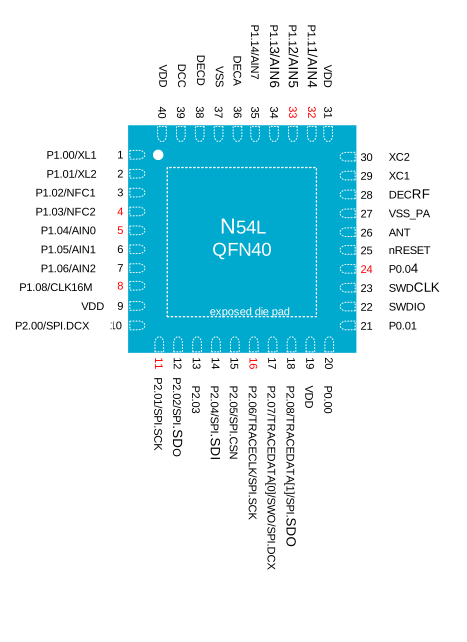
| Pin | Clock pin | Name | Function | Description | Dedicated function |
|---|---|---|---|---|---|
| 1 |
| P1.00 XL1 | Digital I/O Analog input | General purpose I/O Connection for 32.768 kHz crystal |
|
| 2 |
| P1.01 XL2 | Digital I/O Analog input | General purpose I/O Connection for 32.768 kHz crystal |
|
| 3 |
| P1.02 NFC1 | Digital I/O NFC input | General purpose I/O NFC antenna connection |
|
| 4 | Yes | P1.03 NFC2 | Digital I/O NFC input | General purpose I/O NFC antenna connection |
|
| 5 | Yes | P1.04 ASO[0] AIN0 | Digital I/O Digital I/O Analog input | General purpose I/O TAMPC active shield 0 output Analog input |
TAMPC
|
| 6 |
| P1.05 ASI[0] RADIO[6] AIN1 | Digital I/O Digital I/O Digital I/O Analog input | General purpose I/O TAMPC active shield 0 input RADIO DFEGPIO Analog input |
TAMPC RADIO
|
| 7 |
| P1.06 ASO[1] AIN2 | Digital I/O Digital I/O Analog input | General purpose I/O TAMPC active shield 1 output Analog input |
TAMPC
|
| 8 | Yes | P1.08
EXTREF | Digital I/O Digital I/O Analog input | General purpose I/O GRTC CLKOUTFAST External reference for SAADC |
|
| 9 |
| VDD | Power | Power supply |
|
| 10 |
| P2.00
| Digital I/O Digital I/O Digital I/O Digital I/O Digital I/O | General purpose I/O SPIM DCX UARTE RXD FLPR.4 QSPI D3 |
SPIM00/20 UARTE00/20 FLPR FLPR (QSPI) |
| 11 | Yes | P2.01
| Digital I/O Digital I/O Digital I/O Digital I/O Digital I/O | General purpose I/O SPIM SCK SPIS SCK FLPR.0 QSPI SCK |
SPIM00/20 SPIS00/20 FLPR FLPR (QSPI |
| 12 |
| P2.02
| Digital I/O Digital I/O Digital I/O Digital I/O Digital I/O Digital I/O | General purpose I/O SPIM SDO SPIS SDO UARTE TXD FLPR.1 QSPI D0 |
SPIM00/20 SPIS00/20 UARTE00/20 FLPR FLPR (QSPI)
|
| 13 |
| P2.03
| Digital I/O Digital I/O Digital I/O | General purpose I/O FLPR.3 QSPI D2 |
FLPR FLPR (QSPI) |
| 14 |
| P2.04
| Digital I/O Digital I/O Digital I/O Digital I/O Digital I/O Digital I/O | General purpose I/O SPIM SDI SPIS SDI UARTE CTS FLPR.2 QSPI D1 |
SPIM00/20 SPIS00/20 UARTE00/20 FLPR FLPR (QSPI)
|
| 15 |
| P2.05
| Digital I/O Digital I/O Digital I/O Digital I/O Digital I/O Digital I/O | General purpose I/O SPIM CSN SPIS CSN UARTE RTS FLPR.5 QSPI CSN |
SPIM00/20 SPIS00/20 UARTE00/20 FLPR FLPR (QSPI) |
| 16 | Yes | P2.06
TRACECLK | Digital I/O Digital I/O Digital I/O Digital I/O Digital I/O | General purpose I/O FLPR.6 SPIM SCK SPIS SCK Trace clock |
FLPR SPIM00/21 SPIS00/21 Trace |
| 17 |
| P2.07
TRACEDATA[0] SWO
| Digital I/O Digital I/O Digital I/O Digital I/O Digital I/O Digital I/O | General purpose I/O FLPR.7 Trace data Serial wire output (SWO) SPIM DCX UARTE RXD |
FLPR Trace Trace SPIM00/21 UARTE00/21 |
| 18 |
| P2.08
TRACEDATA[1]
| Digital I/O Digital I/O Digital I/O Digital I/O Digital I/O Digital I/O | General purpose I/O FLPR.8 Trace data SPIM SDO SPIS SDO UARTE TXD |
FLPR Trace SPIM00/21 SPIS00/21 UARTE00/21 |
| 19 |
| VDD | Power | Power supply |
|
| 20 |
| P0.00 | Digital I/O | General purpose I/O |
|
| 21 |
| P0.01 | Digital I/O | General purpose I/O |
|
| 22 |
| SWDIO | Debug | Serial wire data. Bidirectional with standard-drive and on-chip pull-up. |
|
| 23 |
| SWDCLK | Debug | Serial wire clock. Input with on-chip pull-down. |
|
| 24 | Yes | P0.04
| Digital I/O Digital I/O | General purpose I/O GRTC CLKOUT32K |
GRTC |
| 25 |
| nRESET | Reset | Pin reset with on-chip pull-up |
|
| 26 |
| ANT | RF | Single ended radio antenna connection | See Reference circuitry for guidelines on how to ensure good RF performance |
| 27 |
| VSS_PA | Power | Ground (radio supply) |
|
| 28 |
| DECRF | Power | 0.9 V regulator supply decoupling | Must be connected to DECA. See Reference circuitry. |
| 29 |
| XC1 | Analog input | Connection for 32 MHz crystal |
|
| 30 |
| XC2 | Analog input | Connection for 32 MHz crystal |
|
| 31 |
| VDD | Power | Power supply |
|
| 32 | Yes | P1.11 ASO[3] RADIO[2] AIN4 | Digital I/O Digital I/O Digital I/O Analog input | General purpose I/O TAMPC active shield 3 output RADIO DFEGPIO Analog input |
TAMPC RADIO
|
| 33 | Yes | P1.12 ASI[3] RADIO[3] AIN5 | Digital I/O Digital I/O Digital I/O Analog input | General purpose I/O TAMPC active shield 3 input RADIO DFEGPIO Analog input |
TAMPC RADIO
|
| 34 |
| P1.13 RADIO[4] AIN6 | Digital I/O Digital I/O Analog input | General purpose I/O RADIO DFEGPIO Analog input |
RADIO
|
| 35 |
| P1.14 RADIO[5] AIN7 | Digital I/O Digital I/O Analog input | General purpose I/O RADIO DFEGPIO Analog input |
RADIO
|
| 36 |
| DECA | Power | 0.9 V regulator supply decoupling | Must be connected to DECRF |
| 37 |
| VSS | Power | Ground |
|
| 38 |
| DECD | Power | 0.9 V regulator supply decoupling |
|
| 39 |
| DCC | Power | DC/DC regulator output |
|
| 40 |
| VDD | Power | Power supply |
|
| 41 |
| VSS | Power | Ground pad (die pad) |
|
For the device to function properly, the exposed die pad (pin 49) must be connected to ground (VSS, pins 32 and 44).
QFN48 (QFAA) package pin assignments
The QFN48 pin assignment figure and table describe the pinouts for this variant of the device.
Pins that can be used as clock signals are shown in as red in the figure. For more information about clock pins, see Clock pins.
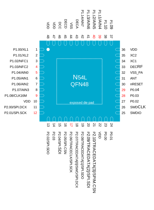
| Pin | Clock pin | Name | Function | Description | Dedicated function |
|---|---|---|---|---|---|
| 1 |
| P1.00 XL1 | Digital I/O Analog input | General purpose I/O Connection for 32.768 kHz crystal |
|
| 2 |
| P1.01 XL2 | Digital I/O Analog input | General purpose I/O Connection for 32.768 kHz crystal |
|
| 3 |
| P1.02 NFC1 | Digital I/O NFC input | General purpose I/O NFC antenna connection |
|
| 4 | Yes | P1.03 NFC2 | Digital I/O NFC input | General purpose I/O NFC antenna connection |
|
| 5 | Yes | P1.04 ASO[0] AIN0 | Digital I/O Digital I/O Analog input | General purpose I/O TAMPC active shield 0 output Analog input |
TAMPC
|
| 6 |
| P1.05 ASI[0] RADIO[6] AIN1 | Digital I/O Digital I/O Digital I/O Analog input | General purpose I/O TAMPC active shield 0 input RADIO DFEGPIO Analog input |
TAMPC RADIO
|
| 7 |
| P1.06 ASO[1] AIN2 | Digital I/O Digital I/O Analog input | General purpose I/O TAMPC active shield 1 output Analog input |
TAMPC
|
| 8 |
| P1.07 ASI[1] AIN3 | Digital I/O Digital I/O Analog input | General purpose I/O TAMPC active shield 1 input Analog input |
TAMPC
|
| 9 | Yes | P1.08
EXTREF | Digital I/O Digital I/O Analog input | General purpose I/O GRTC CLKOUTFAST External reference for SAADC |
|
| 10 |
| VDD | Power | Power supply |
|
| 11 |
| P2.00
| Digital I/O Digital I/O Digital I/O Digital I/O Digital I/O | General purpose I/O SPIM DCX UARTE RXD FLPR.4 QSPI D3 |
SPIM00/20 UARTE00/20 FLPR FLPR (QSPI) |
| 12 | Yes | P2.01
| Digital I/O Digital I/O Digital I/O Digital I/O Digital I/O | General purpose I/O SPIM SCK SPIS SCK FLPR.0 QSPI SCK |
SPIM00/20 SPIS00/20 FLPR FLPR (QSPI |
| 13 |
| P2.02
| Digital I/O Digital I/O Digital I/O Digital I/O Digital I/O Digital I/O | General purpose I/O SPIM SDO SPIS SDO UARTE TXD FLPR.1 QSPI D0 |
SPIM00/20 SPIS00/20 UARTE00/20 FLPR FLPR (QSPI)
|
| 14 |
| P2.03
| Digital I/O Digital I/O Digital I/O | General purpose I/O FLPR.3 QSPI D2 |
FLPR FLPR (QSPI) |
| 15 |
| P2.04
| Digital I/O Digital I/O Digital I/O Digital I/O Digital I/O Digital I/O | General purpose I/O SPIM SDI SPIS SDI UARTE CTS FLPR.2 QSPI D1 |
SPIM00/20 SPIS00/20 UARTE00/20 FLPR FLPR (QSPI)
|
| 16 |
| P2.05
| Digital I/O Digital I/O Digital I/O Digital I/O Digital I/O Digital I/O | General purpose I/O SPIM CSN SPIS CSN UARTE RTS FLPR.5 QSPI CSN |
SPIM00/20 SPIS00/20 UARTE00/20 FLPR FLPR (QSPI) |
| 17 | Yes | P2.06
TRACECLK | Digital I/O Digital I/O Digital I/O Digital I/O Digital I/O | General purpose I/O FLPR.6 SPIM SCK SPIS SCK Trace clock |
FLPR SPIM00/21 SPIS00/21 Trace |
| 18 |
| P2.07
TRACEDATA[0] SWO
| Digital I/O Digital I/O Digital I/O Digital I/O Digital I/O Digital I/O | General purpose I/O FLPR.7 Trace data Serial wire output (SWO) SPIM DCX UARTE RXD |
FLPR Trace Trace SPIM00/21 UARTE00/21 |
| 19 |
| P2.08
TRACEDATA[1]
| Digital I/O Digital I/O Digital I/O Digital I/O Digital I/O Digital I/O | General purpose I/O FLPR.8 Trace data SPIM SDO SPIS SDO UARTE TXD |
FLPR Trace SPIM00/21 SPIS00/21 UARTE00/21 |
| 20 |
| P2.09
TRACEDATA[2]
| Digital I/O Digital I/O Digital I/O Digital I/O Digital I/O Digital I/O | General purpose I/O FLPR.9 Trace data SPIM SDI SPIS SDI UARTE CTS |
FLPR Trace SPIM00/21 SPIS00/21 UARTE00/21 |
| 21 |
| P2.10
TRACEDATA[3]
| Digital I/O Digital I/O Digital I/O Digital I/O Digital I/O Digital I/O | General purpose I/O FLPR.10 Trace data SPIM CSN SPIS CSN UARTE RTS |
FLPR Trace SPIM00/21 SPIS00/21 UARTE00/21 |
| 22 |
| VDD | Power | Power supply |
|
| 23 |
| P0.00 | Digital I/O | General purpose I/O |
|
| 24 |
| P0.01 | Digital I/O | General purpose I/O |
|
| 25 |
| SWDIO | Debug | Serial wire data. Bidirectional with standard-drive and on-chip pull-up. |
|
| 26 |
| SWDCLK | Debug | Serial wire clock. Input with on-chip pull-down. |
|
| 27 |
| P0.02 | Digital I/O | General purpose I/O |
|
| 28 | Yes | P0.03
| Digital I/O Digital I/O | General purpose I/O GRTC PWM |
GRTC
|
| 29 | Yes | P0.04
| Digital I/O Digital I/O | General purpose I/O GRTC CLKOUT32K |
GRTC |
| 30 |
| nRESET | Reset | Pin reset with on-chip pull-up |
|
| 31 |
| ANT | RF | Single ended radio antenna connection | See Reference circuitry for guidelines on how to ensure good RF performance |
| 32 |
| VSS_PA | Power | Ground (radio supply) |
|
| 33 |
| DECRF | Power | 0.9 V regulator supply decoupling | Must be connected to DECA. See Reference circuitry. |
| 34 |
| XC1 | Analog input | Connection for 32 MHz crystal |
|
| 35 |
| XC2 | Analog input | Connection for 32 MHz crystal |
|
| 36 |
| VDD | Power | Power supply |
|
| 37 |
| P1.09 ASO[2] RADIO[0] | Digital I/O Digital I/O Digital I/O | General purpose I/O TAMPC active shield 2 output RADIO DFEGPIO |
TAMPC RADIO
|
| 38 |
| P1.10 ASI[2] RADIO[1] | Digital I/O Digital I/O Digital I/O | General purpose I/O TAMPC active shield 2 input RADIO DFEGPIO |
TAMPC RADIO
|
| 39 | Yes | P1.11 ASO[3] RADIO[2] AIN4 | Digital I/O Digital I/O Digital I/O Analog input | General purpose I/O TAMPC active shield 3 output RADIO DFEGPIO Analog input |
TAMPC RADIO
|
| 40 | Yes | P1.12 ASI[3] RADIO[3] AIN5 | Digital I/O Digital I/O Digital I/O Analog input | General purpose I/O TAMPC active shield 3 input RADIO DFEGPIO Analog input |
TAMPC RADIO
|
| 41 |
| P1.13 RADIO[4] AIN6 | Digital I/O Digital I/O Analog input | General purpose I/O RADIO DFEGPIO Analog input |
RADIO
|
| 42 |
| P1.14 RADIO[5] AIN7 | Digital I/O Digital I/O Analog input | General purpose I/O RADIO DFEGPIO Analog input |
RADIO
|
| 43 |
| DECA | Power | 0.9 V regulator supply decoupling | Must be connected to DECRF |
| 44 |
| VSS | Power | Ground |
|
| 45 |
| DECD | Power | 0.9 V regulator supply decoupling |
|
| 46 |
| DCC | Power | DC/DC regulator output |
|
| 47 |
| VDD | Power | Power supply |
|
| 48 |
| VDD | Power | Power supply |
|
| 49 |
| VSS | Power | Ground pad (die pad) |
|
For the device to function properly, the exposed die pad (pin 49) must be connected to ground (VSS, pins 32 and 44).
QFN52 (QGAA) package pin assignments
The QFN52 pin assignment figure and table describe the pinouts for this variant of the device.
Pins that can be used as clock signals are shown in as red in the figure. For more information about clock pins, see Clock pins.
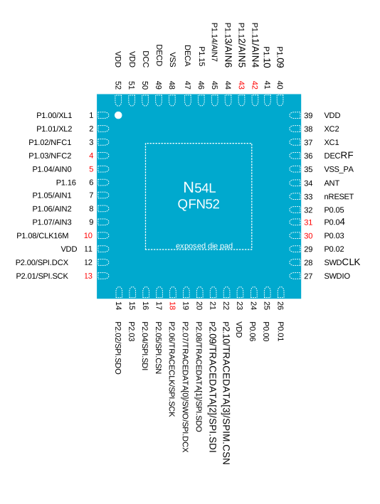
| Pin | Clock pin | Name | Function | Description | Dedicated function |
|---|---|---|---|---|---|
| 1 |
| P1.00 XL1 | Digital I/O Analog input | General purpose I/O Connection for 32.768 kHz crystal |
|
| 2 |
| P1.01 XL2 | Digital I/O Analog input | General purpose I/O Connection for 32.768 kHz crystal |
|
| 3 |
| P1.02 NFC1 | Digital I/O NFC input | General purpose I/O NFC antenna connection |
|
| 4 | Yes | P1.03 NFC2 | Digital I/O NFC input | General purpose I/O NFC antenna connection |
|
| 5 | Yes | P1.04 ASO[0] AIN0 | Digital I/O Digital I/O Analog input | General purpose I/O TAMPC active shield 0 output Analog input |
TAMPC
|
| 6 |
| P1.16 | Digital I/O | General purpose I/O |
|
| 7 |
| P1.05 ASI[0] RADIO[6] AIN1 | Digital I/O Digital I/O Digital I/O Analog input | General purpose I/O TAMPC active shield 0 input RADIO DFEGPIO Analog input |
TAMPC RADIO
|
| 8 |
| P1.06 ASO[1] AIN2 | Digital I/O Digital I/O Analog input | General purpose I/O TAMPC active shield 1 output Analog input |
TAMPC
|
| 9 |
| P1.07 ASI[1] AIN3 | Digital I/O Digital I/O Analog input | General purpose I/O TAMPC active shield 1 input Analog input |
TAMPC
|
| 10 | Yes | P1.08
EXTREF | Digital I/O Digital I/O Analog input | General purpose I/O GRTC CLKOUTFAST External reference for SAADC |
|
| 11 |
| VDD | Power | Power supply |
|
| 12 |
| P2.00
| Digital I/O Digital I/O Digital I/O Digital I/O Digital I/O | General purpose I/O SPIM DCX UARTE RXD FLPR.4 QSPI D3 |
SPIM00/20 UARTE00/20 FLPR FLPR (QSPI) |
| 13 | Yes | P2.01
| Digital I/O Digital I/O Digital I/O Digital I/O Digital I/O | General purpose I/O SPIM SCK SPIS SCK FLPR.0 QSPI SCK |
SPIM00/20 SPIS00/20 FLPR FLPR (QSPI |
| 14 |
| P2.02
| Digital I/O Digital I/O Digital I/O Digital I/O Digital I/O Digital I/O | General purpose I/O SPIM SDO SPIS SDO UARTE TXD FLPR.1 QSPI D0 |
SPIM00/20 SPIS00/20 UARTE00/20 FLPR FLPR (QSPI)
|
| 15 |
| P2.03
| Digital I/O Digital I/O Digital I/O | General purpose I/O FLPR.3 QSPI D2 |
FLPR FLPR (QSPI) |
| 16 |
| P2.04
| Digital I/O Digital I/O Digital I/O Digital I/O Digital I/O Digital I/O | General purpose I/O SPIM SDI SPIS SDI UARTE CTS FLPR.2 QSPI D1 |
SPIM00/20 SPIS00/20 UARTE00/20 FLPR FLPR (QSPI)
|
| 17 |
| P2.05
| Digital I/O Digital I/O Digital I/O Digital I/O Digital I/O Digital I/O | General purpose I/O SPIM CSN SPIS CSN UARTE RTS FLPR.5 QSPI CSN |
SPIM00/20 SPIS00/20 UARTE00/20 FLPR FLPR (QSPI) |
| 18 | Yes | P2.06
TRACECLK | Digital I/O Digital I/O Digital I/O Digital I/O Digital I/O | General purpose I/O FLPR.6 SPIM SCK SPIS SCK Trace clock |
FLPR SPIM00/21 SPIS00/21 Trace |
| 19 |
| P2.07
TRACEDATA[0] SWO
| Digital I/O Digital I/O Digital I/O Digital I/O Digital I/O Digital I/O | General purpose I/O FLPR.7 Trace data Serial wire output (SWO) SPIM DCX UARTE RXD |
FLPR Trace Trace SPIM00/21 UARTE00/21 |
| 20 |
| P2.08
TRACEDATA[1]
| Digital I/O Digital I/O Digital I/O Digital I/O Digital I/O Digital I/O | General purpose I/O FLPR.8 Trace data SPIM SDO SPIS SDO UARTE TXD |
FLPR Trace SPIM00/21 SPIS00/21 UARTE00/21 |
| 21 |
| P2.09
TRACEDATA[2]
| Digital I/O Digital I/O Digital I/O Digital I/O Digital I/O Digital I/O | General purpose I/O FLPR.9 Trace data SPIM SDI SPIS SDI UARTE CTS |
FLPR Trace SPIM00/21 SPIS00/21 UARTE00/21 |
| 22 |
| P2.10
TRACEDATA[3]
| Digital I/O Digital I/O Digital I/O Digital I/O Digital I/O Digital I/O | General purpose I/O FLPR.10 Trace data SPIM CSN SPIS CSN UARTE RTS |
FLPR Trace SPIM00/21 SPIS00/21 UARTE00/21 |
| 23 |
| VDD | Power | Power supply |
|
| 24 |
| P0.06 | Digital I/O | General purpose I/O |
|
| 25 |
| P0.00 | Digital I/O | General purpose I/O |
|
| 26 |
| P0.01 | Digital I/O | General purpose I/O |
|
| 27 |
| SWDIO | Debug | Serial wire data. Bidirectional with standard-drive and on-chip pull-up. |
|
| 28 |
| SWDCLK | Debug | Serial wire clock. Input with on-chip pull-down. |
|
| 29 |
| P0.02 | Digital I/O | General purpose I/O |
|
| 30 | Yes | P0.03
| Digital I/O Digital I/O | General purpose I/O GRTC PWM |
GRTC
|
| 31 | Yes | P0.04
| Digital I/O Digital I/O | General purpose I/O GRTC CLKOUT32K |
GRTC |
| 32 |
| P0.05 | Digital I/O | General purpose I/O |
|
| 33 |
| nRESET | Reset | Pin reset with on-chip pull-up |
|
| 34 |
| ANT | RF | Single ended radio antenna connection | See Reference circuitry for guidelines on how to ensure good RF performance |
| 35 |
| VSS_PA | Power | Ground (radio supply) |
|
| 36 |
| DECRF | Power | 0.9 V regulator supply decoupling | Must be connected to DECA. See Reference circuitry. |
| 37 |
| XC1 | Analog input | Connection for 32 MHz crystal |
|
| 38 |
| XC2 | Analog input | Connection for 32 MHz crystal |
|
| 39 |
| VDD | Power | Power supply |
|
| 40 |
| P1.09 ASO[2] RADIO[0] | Digital I/O Digital I/O Digital I/O | General purpose I/O TAMPC active shield 2 output RADIO DFEGPIO |
TAMPC RADIO
|
| 41 |
| P1.10 ASI[2] RADIO[1] | Digital I/O Digital I/O Digital I/O | General purpose I/O TAMPC active shield 2 input RADIO DFEGPIO |
TAMPC RADIO
|
| 42 | Yes | P1.11 ASO[3] RADIO[2] AIN4 | Digital I/O Digital I/O Digital I/O Analog input | General purpose I/O TAMPC active shield 3 output RADIO DFEGPIO Analog input |
TAMPC RADIO
|
| 43 | Yes | P1.12 ASI[3] RADIO[3] AIN5 | Digital I/O Digital I/O Digital I/O Analog input | General purpose I/O TAMPC active shield 3 input RADIO DFEGPIO Analog input |
TAMPC RADIO
|
| 44 |
| P1.13 RADIO[4] AIN6 | Digital I/O Digital I/O Analog input | General purpose I/O RADIO DFEGPIO Analog input |
RADIO
|
| 45 |
| P1.14 RADIO[5] AIN7 | Digital I/O Digital I/O Analog input | General purpose I/O RADIO DFEGPIO Analog input |
RADIO
|
| 46 |
| P1.15 | Digital I/O | General purpose I/O |
|
| 47 |
| DECA | Power | 0.9 V regulator supply decoupling | Must be connected to DECRF |
| 48 |
| VSS | Power | Ground |
|
| 49 |
| DECD | Power | 0.9 V regulator supply decoupling |
|
| 50 |
| DCC | Power | DC/DC regulator output |
|
| 51 |
| VDD | Power | Power supply |
|
| 52 |
| VDD | Power | Power supply |
|
| 53 |
| VSS | Power | Ground pad (die pad) |
|
For the device to function properly, the exposed die pad (pin 49) must be connected to ground (VSS, pins 32 and 44).
CSP47 (CAAA) package pin assignments
The CSP47 pin assignment figure and table describe the pinouts for this variant of the device.
Pins that can be used as clock signals are shown in as red in the figure. For more information about clock pins, see Clock pins.
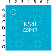
| Pin | Clock pin | Name | Function | Description | Dedicated function |
|---|---|---|---|---|---|
| A1 |
| XC1 | Analog input | Connection for 32 MHz crystal |
|
| A2 |
| XC2 | Analog input | Connection for 32 MHz crystal |
|
| A3 | Yes | P1.12 ASI[3] RADIO[3] AIN5 | Digital I/O Digital I/O Digital I/O Analog input | General purpose I/O TAMPC active shield 3 input RADIO DFEGPIO Analog input |
TAMPC RADIO
|
| A4 |
| DECA | Power | 0.9 V regulator supply decoupling | Must be connected to DECRF |
| A5 |
| DECD | Power | 0.9 V regulator supply decoupling |
|
| A6 |
| VSS | Power | Ground |
|
| A7 |
| DCC | Power | DC/DC regulator output |
|
| B1 |
| DECRF | Power | 0.9 V regulator supply decoupling | Must be connected to DECA. See Reference circuitry. |
| B3 |
| P1.09 ASO[2] RADIO[0] | Digital I/O Digital I/O Digital I/O | General purpose I/O TAMPC active shield 2 output RADIO DFEGPIO |
TAMPC RADIO
|
| B4 |
| P1.13 RADIO[4] AIN6 | Digital I/O Digital I/O Analog input | General purpose I/O RADIO DFEGPIO Analog input |
RADIO
|
| B5 |
| P1.14 RADIO[5] AIN7 | Digital I/O Digital I/O Analog input | General purpose I/O RADIO DFEGPIO Analog input |
RADIO
|
| B6 |
| P1.15 | Digital I/O | General purpose I/O |
|
| B7 |
| VDD | Power | Power supply |
|
| C2 |
| VSS_PA | Power | Ground (radio supply) |
|
| C3 |
| P1.10 ASI[2] RADIO[1] | Digital I/O Digital I/O Digital I/O | General purpose I/O TAMPC active shield 2 input RADIO DFEGPIO |
TAMPC RADIO
|
| C4 | Yes | P1.11 ASO[3] RADIO[2] AIN4 | Digital I/O Digital I/O Digital I/O Analog input | General purpose I/O TAMPC active shield 3 output RADIO DFEGPIO Analog input |
TAMPC RADIO
|
| C5 |
| P1.00 XL1 | Digital I/O Analog input | General purpose I/O Connection for 32.768 kHz crystal |
|
| C6 |
| P1.01 XL2 | Digital I/O Analog input | General purpose I/O Connection for 32.768 kHz crystal |
|
| C7 |
| P1.02 NFC1 | Digital I/O NFC input | General purpose I/O NFC antenna connection |
|
| D1 |
| ANT | RF | Single ended radio antenna connection | See Reference circuitry for guidelines on how to ensure good RF performance |
| D2 |
| nRESET | Reset | Pin reset with on-chip pull-up |
|
| D3 | Yes | P0.04
| Digital I/O Digital I/O | General purpose I/O GRTC CLKOUT32K |
GRTC |
| D4 |
| P2.08
TRACEDATA[1]
| Digital I/O Digital I/O Digital I/O Digital I/O Digital I/O Digital I/O | General purpose I/O FLPR.8 Trace data SPIM SDO SPIS SDO UARTE TXD |
FLPR Trace SPIM00/21 SPIS00/21 UARTE00/21 |
| D5 | Yes | P1.03 NFC2 | Digital I/O NFC input | General purpose I/O NFC antenna connection |
|
| D6 | Yes | P1.04 ASO[0] AIN0 | Digital I/O Digital I/O Analog input | General purpose I/O TAMPC active shield 0 output Analog input |
TAMPC
|
| D7 |
| P1.06 ASO[1] AIN2 | Digital I/O Digital I/O Analog input | General purpose I/O TAMPC active shield 1 output Analog input |
TAMPC
|
| E1 | Yes | P0.03
| Digital I/O Digital I/O | General purpose I/O GRTC PWM |
GRTC
|
| E2 |
| P0.02 | Digital I/O | General purpose I/O |
|
| E3 |
| SWDCLK | Debug | Serial wire clock. Input with on-chip pull-down. |
|
| E4 |
| P2.07
TRACEDATA[0] SWO
| Digital I/O Digital I/O Digital I/O Digital I/O Digital I/O Digital I/O | General purpose I/O FLPR.7 Trace data Serial wire output (SWO) SPIM DCX UARTE RXD |
FLPR Trace Trace SPIM00/21 UARTE00/21 |
| E5 |
| P2.03
| Digital I/O Digital I/O Digital I/O | General purpose I/O FLPR.3 QSPI D2 |
FLPR FLPR (QSPI) |
| E6 |
| P1.05 ASI[0] RADIO[6] AIN1 | Digital I/O Digital I/O Digital I/O Analog input | General purpose I/O TAMPC active shield 0 input RADIO DFEGPIO Analog input |
TAMPC RADIO
|
| E7 |
| P1.07 ASI[1] AIN3 | Digital I/O Digital I/O Analog input | General purpose I/O TAMPC active shield 1 input Analog input |
TAMPC
|
| F1 |
| P0.01 | Digital I/O | General purpose I/O |
|
| F2 |
| SWDIO | Debug | Serial wire data. Bidirectional with standard-drive and on-chip pull-up. |
|
| F3 |
| P2.09
TRACEDATA[2]
| Digital I/O Digital I/O Digital I/O Digital I/O Digital I/O Digital I/O | General purpose I/O FLPR.9 Trace data SPIM SDI SPIS SDI UARTE CTS |
FLPR Trace SPIM00/21 SPIS00/21 UARTE00/21 |
| F4 | Yes | P2.06
TRACECLK | Digital I/O Digital I/O Digital I/O Digital I/O Digital I/O | General purpose I/O FLPR.6 SPIM SCK SPIS SCK Trace clock |
FLPR SPIM00/21 SPIS00/21 Trace |
| F5 |
| P2.04
| Digital I/O Digital I/O Digital I/O Digital I/O Digital I/O Digital I/O | General purpose I/O SPIM SDI SPIS SDI UARTE CTS FLPR.2 QSPI D1 |
SPIM00/20 SPIS00/20 UARTE00/20 FLPR FLPR (QSPI)
|
| F6 |
| P2.02
| Digital I/O Digital I/O Digital I/O Digital I/O Digital I/O Digital I/O | General purpose I/O SPIM SDO SPIS SDO UARTE TXD FLPR.1 QSPI D0 |
SPIM00/20 SPIS00/20 UARTE00/20 FLPR FLPR (QSPI)
|
| F7 | Yes | P1.08
EXTREF | Digital I/O Digital I/O Analog input | General purpose I/O GRTC CLKOUTFAST External reference for SAADC |
|
| G1 |
| P0.00 | Digital I/O | General purpose I/O |
|
| G2 |
| P2.10
TRACEDATA[3]
| Digital I/O Digital I/O Digital I/O Digital I/O Digital I/O Digital I/O | General purpose I/O FLPR.10 Trace data SPIM CSN SPIS CSN UARTE RTS |
FLPR Trace SPIM00/21 SPIS00/21 UARTE00/21 |
| G3 |
| VDD | Power | Power supply |
|
| G4 |
| VSS | Power | Ground |
|
| G5 |
| P2.05
| Digital I/O Digital I/O Digital I/O Digital I/O Digital I/O Digital I/O | General purpose I/O SPIM CSN SPIS CSN UARTE RTS FLPR.5 QSPI CSN |
SPIM00/20 SPIS00/20 UARTE00/20 FLPR FLPR (QSPI) |
| G6 |
| P2.00
| Digital I/O Digital I/O Digital I/O Digital I/O Digital I/O | General purpose I/O SPIM DCX UARTE RXD FLPR.4 QSPI D3 |
SPIM00/20 UARTE00/20 FLPR FLPR (QSPI) |
| G7 | Yes | P2.01
| Digital I/O Digital I/O Digital I/O Digital I/O Digital I/O | General purpose I/O SPIM SCK SPIS SCK FLPR.0 QSPI SCK |
SPIM00/20 SPIS00/20 FLPR FLPR (QSPI |
For the device to function properly, the exposed die pad (pin 49) must be connected to ground (VSS, pins 32 and 44).