REGULATORS — Regulator control
The power supply consists of a number of LDO and DC/DC regulators that maximize the system's power efficiency.
All system components are powered from the main on-chip voltage regulator VREGMAIN. The regulator converts the voltage supplied on VDD to internal voltage.
The device also has an USB regulator, which only powers the USB physical interface. It will not power the device. The USB regulator is documented in USBREG — USB regulator control.
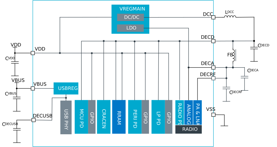
The main supply voltage is connected to the VDD pin.
VREGMAIN — Main regulator
VREGMAIN is the main regulator of the system.
The device only supports DC/DC mode, which needs external components. For details, see Reference circuitry.
VREGMAIN starts up using a fall-back mode, and the DC/DC regulator must be enabled using register VREGMAIN.DCDCEN.
Inductor detection
The DC/DC regulator requires an external inductor connected to the DCC pin. If an inductor is not present, the regulator stays in fall-back mode to enable a soft shut-down of the system. Register VREGMAIN.INDUCTORDET reports the inductor detection status and can be used to detect inductor failures that prevent DC/DC operation.
Registers
Instances
| Instance | Domain | Base address | TrustZone | Split access | Description | ||
|---|---|---|---|---|---|---|---|
| Map | Att | DMA | |||||
REGULATORS : S | GLOBAL | 0x50120000 | US | S | NA | No | Regulator control |
Register overview
| Register | Offset | TZ | Description |
|---|---|---|---|
| SYSTEMOFF | 0x500 | System OFF register | |
| POFCON | 0x530 | Power-fail comparator configuration | |
| POFSTAT | 0x534 | Power-fail comparator status register | |
| VREGMAIN.DCDCEN | 0x600 | Enable DC/DC converter | |
| VREGMAIN.INDUCTORDET | 0x604 | VREGMAIN inductor detection |
SYSTEMOFF
Address offset: 0x500
System OFF register
| Bit number | 31 | 30 | 29 | 28 | 27 | 26 | 25 | 24 | 23 | 22 | 21 | 20 | 19 | 18 | 17 | 16 | 15 | 14 | 13 | 12 | 11 | 10 | 9 | 8 | 7 | 6 | 5 | 4 | 3 | 2 | 1 | 0 | |||
|---|---|---|---|---|---|---|---|---|---|---|---|---|---|---|---|---|---|---|---|---|---|---|---|---|---|---|---|---|---|---|---|---|---|---|---|
| ID | A | ||||||||||||||||||||||||||||||||||
| Reset 0x00000000 | 0 | 0 | 0 | 0 | 0 | 0 | 0 | 0 | 0 | 0 | 0 | 0 | 0 | 0 | 0 | 0 | 0 | 0 | 0 | 0 | 0 | 0 | 0 | 0 | 0 | 0 | 0 | 0 | 0 | 0 | 0 | 0 | |||
| ID | R/W | Field | Value ID | Value | Description | ||||||||||||||||||||||||||||||
| A | W | SYSTEMOFF | Enable System OFF mode | ||||||||||||||||||||||||||||||||
Enter | 1 | Enable System OFF mode | |||||||||||||||||||||||||||||||||
POFCON
Address offset: 0x530
Power-fail comparator configuration
| Bit number | 31 | 30 | 29 | 28 | 27 | 26 | 25 | 24 | 23 | 22 | 21 | 20 | 19 | 18 | 17 | 16 | 15 | 14 | 13 | 12 | 11 | 10 | 9 | 8 | 7 | 6 | 5 | 4 | 3 | 2 | 1 | 0 | |||
|---|---|---|---|---|---|---|---|---|---|---|---|---|---|---|---|---|---|---|---|---|---|---|---|---|---|---|---|---|---|---|---|---|---|---|---|
| ID | C | B | B | B | B | A | |||||||||||||||||||||||||||||
| Reset 0x00000000 | 0 | 0 | 0 | 0 | 0 | 0 | 0 | 0 | 0 | 0 | 0 | 0 | 0 | 0 | 0 | 0 | 0 | 0 | 0 | 0 | 0 | 0 | 0 | 0 | 0 | 0 | 0 | 0 | 0 | 0 | 0 | 0 | |||
| ID | R/W | Field | Value ID | Value | Description | ||||||||||||||||||||||||||||||
| A | RW | POF | Enable or disable power-fail comparator | ||||||||||||||||||||||||||||||||
Disabled | 0 | Disable | |||||||||||||||||||||||||||||||||
Enabled | 1 | Enable | |||||||||||||||||||||||||||||||||
| B | RW | THRESHOLD | Power-fail comparator threshold setting | ||||||||||||||||||||||||||||||||
V17 | 0 | Set threshold to 1.7 V for VDD | |||||||||||||||||||||||||||||||||
V18 | 1 | Set threshold to 1.8 V for VDD | |||||||||||||||||||||||||||||||||
V19 | 2 | Set threshold to 1.9 V for VDD | |||||||||||||||||||||||||||||||||
V20 | 3 | Set threshold to 2.0 V for VDD | |||||||||||||||||||||||||||||||||
V21 | 4 | Set threshold to 2.1 V for VDD | |||||||||||||||||||||||||||||||||
V22 | 5 | Set threshold to 2.2 V for VDD | |||||||||||||||||||||||||||||||||
V23 | 6 | Set threshold to 2.3 V for VDD | |||||||||||||||||||||||||||||||||
V24 | 7 | Set threshold to 2.4 V for VDD | |||||||||||||||||||||||||||||||||
V25 | 8 | Set threshold to 2.5 V for VDD | |||||||||||||||||||||||||||||||||
V26 | 9 | Set threshold to 2.6 V for VDD | |||||||||||||||||||||||||||||||||
V27 | 10 | Set threshold to 2.7 V for VDD | |||||||||||||||||||||||||||||||||
V28 | 11 | Set threshold to 2.8 V for VDD | |||||||||||||||||||||||||||||||||
V29 | 12 | Set threshold to 2.9 V for VDD | |||||||||||||||||||||||||||||||||
V30 | 13 | Set threshold to 3.0 V for VDD | |||||||||||||||||||||||||||||||||
V31 | 14 | Set threshold to 3.1 V for VDD | |||||||||||||||||||||||||||||||||
V32 | 15 | Set threshold to 3.2 V for VDD | |||||||||||||||||||||||||||||||||
| C | RW | EVENTDISABLE | Disable the POFWARN power-fail warning event | ||||||||||||||||||||||||||||||||
Enabled | 0 | POFWARN event is generated | |||||||||||||||||||||||||||||||||
Disabled | 1 | POFWARN event is not generated | |||||||||||||||||||||||||||||||||
POFSTAT
Address offset: 0x534
Power-fail comparator status register
| Bit number | 31 | 30 | 29 | 28 | 27 | 26 | 25 | 24 | 23 | 22 | 21 | 20 | 19 | 18 | 17 | 16 | 15 | 14 | 13 | 12 | 11 | 10 | 9 | 8 | 7 | 6 | 5 | 4 | 3 | 2 | 1 | 0 | |||
|---|---|---|---|---|---|---|---|---|---|---|---|---|---|---|---|---|---|---|---|---|---|---|---|---|---|---|---|---|---|---|---|---|---|---|---|
| ID | A | ||||||||||||||||||||||||||||||||||
| Reset 0x00000000 | 0 | 0 | 0 | 0 | 0 | 0 | 0 | 0 | 0 | 0 | 0 | 0 | 0 | 0 | 0 | 0 | 0 | 0 | 0 | 0 | 0 | 0 | 0 | 0 | 0 | 0 | 0 | 0 | 0 | 0 | 0 | 0 | |||
| ID | R/W | Field | Value ID | Value | Description | ||||||||||||||||||||||||||||||
| A | R | COMPARATOR | Power-fail comparator status | ||||||||||||||||||||||||||||||||
Above | 0 | Voltage detected above VPOF threshold | |||||||||||||||||||||||||||||||||
Below | 1 | Voltage detected below VPOF threshold | |||||||||||||||||||||||||||||||||
VREGMAIN
Register interface for main voltage regulator.
VREGMAIN.DCDCEN
Address offset: 0x600
Enable DC/DC converter
| Bit number | 31 | 30 | 29 | 28 | 27 | 26 | 25 | 24 | 23 | 22 | 21 | 20 | 19 | 18 | 17 | 16 | 15 | 14 | 13 | 12 | 11 | 10 | 9 | 8 | 7 | 6 | 5 | 4 | 3 | 2 | 1 | 0 | |||
|---|---|---|---|---|---|---|---|---|---|---|---|---|---|---|---|---|---|---|---|---|---|---|---|---|---|---|---|---|---|---|---|---|---|---|---|
| ID | A | ||||||||||||||||||||||||||||||||||
| Reset 0x00000000 | 0 | 0 | 0 | 0 | 0 | 0 | 0 | 0 | 0 | 0 | 0 | 0 | 0 | 0 | 0 | 0 | 0 | 0 | 0 | 0 | 0 | 0 | 0 | 0 | 0 | 0 | 0 | 0 | 0 | 0 | 0 | 0 | |||
| ID | R/W | Field | Value ID | Value | Description | ||||||||||||||||||||||||||||||
| A | RW | VAL | Enable DC/DC buck converter | ||||||||||||||||||||||||||||||||
Disabled | 0 | Disable DC/DC buck converter | |||||||||||||||||||||||||||||||||
Enabled | 1 | Enable DC/DC converter If inductor is not present (see register VREGMAIN.INDUCTORDET), the DC/DC converter cannot operate | |||||||||||||||||||||||||||||||||
VREGMAIN.INDUCTORDET
Address offset: 0x604
VREGMAIN inductor detection
Ensure that an inductor is connected to the DCC pin. The detection can only take place before the DC/DC converter is enabled.
Note: The DC/DC converter cannot operate without an inductor.
| Bit number | 31 | 30 | 29 | 28 | 27 | 26 | 25 | 24 | 23 | 22 | 21 | 20 | 19 | 18 | 17 | 16 | 15 | 14 | 13 | 12 | 11 | 10 | 9 | 8 | 7 | 6 | 5 | 4 | 3 | 2 | 1 | 0 | |||
|---|---|---|---|---|---|---|---|---|---|---|---|---|---|---|---|---|---|---|---|---|---|---|---|---|---|---|---|---|---|---|---|---|---|---|---|
| ID | A | ||||||||||||||||||||||||||||||||||
| Reset 0x00000000 | 0 | 0 | 0 | 0 | 0 | 0 | 0 | 0 | 0 | 0 | 0 | 0 | 0 | 0 | 0 | 0 | 0 | 0 | 0 | 0 | 0 | 0 | 0 | 0 | 0 | 0 | 0 | 0 | 0 | 0 | 0 | 0 | |||
| ID | R/W | Field | Value ID | Value | Description | ||||||||||||||||||||||||||||||
| A | R | DETECTED | |||||||||||||||||||||||||||||||||
InductorNotDetected | 0 | VREGMAIN inductor not detected | |||||||||||||||||||||||||||||||||
InductorDetected | 1 | VREGMAIN inductor detected | |||||||||||||||||||||||||||||||||