CRACEN — Cryptographic accelerator engine
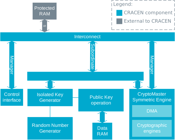
CRACEN (Cryptographic accelerator engine) is a dedicated hardware peripheral that provides a comprehensive set of cryptographic primitives and services to accelerate and harden cryptographic operations on the device.
CRACEN integrates symmetric ciphers, authenticated encryption, public-key arithmetic engines, and high-quality random number generation. It also includes an isolated key generator (IKG) to provision and hold keys securely, reducing exposure of sensitive material to the host CPU and software.
CRACEN is intended to offload compute-intensive and security-sensitive tasks from the main processor: encrypting and decrypting data, computing digests and message authentication codes, performing signature generation and verification, and carrying out key-exchange protocols such as Diffie-Hellman.
The main features of the CRACEN peripheral are the following:
- AES – supports 128- and 256- bit keys, but excludes multi-part operations . Up to 1 MB operation size for AES-CCM and AES-CTR.
- Chacha20-Poly1305, but without multi-part operations
- SHA – SHA1, SHA3, SHA-224, SHA-256, SHA-384, SHA-512
- Public key cryptographic engine (PKE)
- Modular exponentiation – RSA with 4096-bit maximum operand size
- Elliptic curve cryptography (ECC) with 640-bit maximum operand size
- Digital signature algorithm (DSA) and Elliptic curve digital signature algorithm (ECDSA), with 4096-bit maximum operand size
- Diffie-Hellman (D-H and ECD-H) key exchange
- Random number generators (RNG) – NDRNG, including TRNG
- Deterministic random bit generator (DRBG)
- Isolated key generator (IKG) – One asymmetric key and two symmetric (AES) keys
- Counter measures against side channel analysis for PKE and AES
Disclaimer
This section contains an important disclaimer about the CRACEN peripheral documentation.
CRACEN is recommended for use with the libraries in Nordic Semiconductor device SDKs. These libraries are tested and verified to work with the CRACEN hardware. The CRACEN subsystem documentation and register descriptions are for reference only and can be used for modifying the Nordic supplied SDK libraries or implementing new features.
Nordic Semiconductor ASA reserves the right to change the CRACEN documentation and register descriptions without further notice. Changes will not trigger erratas and will not be seen as changing form/fit/function of the device.
Please note that Nordic cannot support questions directly related to the register interface or modification of the source code implementation. Nordic provide support for the top-level API in the software library distributed as part of the device SDK.
Initialization
The CRACEN peripheral is a hardware and software solution where software is delivered as libraries in Nordic device SDKs. Recommended usage of the CRACEN subsystem is to use the SDK library implementation available for the device. The CRACEN subsystem is documented for reference purpose only, please see section Disclaimer for more information.
Before the CRACEN peripheral can be used, it must be configured.
CRACEN is enabled using the ENABLE register. When CRACEN is enabled, it will erase the PKE data RAM by starting a zeroization process. When the PKBUSY field of the PK.STATUS is cleared, the zeroization operation is complete. The PKE engine is not available until the zeroization process has finished.
After CRACEN has been enabled, the CRACENCORE registers can be used.
Each hardware crypto operation category (module) must then be individually enabled. Note that ongoing crypto operations will complete even if the module is disabled during the operation.
PKE data RAM
The PKE data RAM is used by CRACEN as a store for intermediate values when doing cryptographic operations.
| Page number | Access | Zeroization |
|---|---|---|
| 0-7 | Blocked from CPU access | Yes |
| 8-12 | Accessible from the CPU | No |
| 13-15 | Blocked from CPU access | Yes |
Protected RAM
Protected RAM regions can be retained and locked for storing symmetric keys. The CPU cannot access these regions.
After KMU has pushed keys into the protected RAM, PROTECTEDRAMLOCK must be set to Enabled before CRACEN can access and use the keys.
Register PROTECTEDRAMLOCK is a write-once register, and cannot be changed until the next device reset.
The address range of the Protected RAM memory range is defined in Memory.
Countermeasures
CRACEN contains security countermeasures to prevent malicious usage.
- AES – Masking against Simple Power Analysis (SPA) and Differential Power Analysis (DPA)
- IKG/PKE – Protection against timing attacks and DPA
If CRACEN IKG/PKE is used maliciously, a TAMPC event will be generated and countermeasures executed according to the TAMPC configuration. The bits in TAMPC that control the countermeasures have lock bits, preventing further modification to the configuration.
Isolated Key Generator
The Isolated Key Generator (IKG) is a module that derives symmetric and asymmetric keys from the unique seed and optional personalization string.
After IKG has been enabled, CRACEN performs an IKG health test. The CTRDRBGBUSY field of the IKG.STATUS is cleared when the operation has completed. IKG is started by writing to the IKG.START register. The generated IKG keys are valid as long as CRACEN remains enabled. For details on enabling and disabling CRACEN, see ENABLE.
The IKG derives the following keys from seed upon request:
- One 256-bit ECC P-256 key
- Two 256-bit AES keys
Loading seed to IKG
Before keys can be generated, KMU must push the key generation seed used by the IKG to the SEED register and marked as valid.
To create and derive a seed the following sequence of operations are needed.
- Create three 128-bit random numbers using CRACEN RNG.
- Provision the random numbers to KMU slots 0, 1, and 2 (128 bits in each slot).
- SRC.DEST=CRACEN.SEED[n], where n=0, 4, and 8
- SRC.VALUE=random[i], where i=0,1, and 2 (random number results from CRACEN.RND operation in step 1)
- Push the KMU slots where the seed is stored (KMU slots 0, 1, and 2).
- Once all SEED registers have been pushed, CRACEN locks the SEED register and validates the seed for the IKG.
Low power
To ensure lowest possible power consumption when the peripheral is not needed, disable CRACEN.
Make sure any operations are finished before disabling the peripheral in register ENABLE.
Registers
Instances
| Instance | Domain | Base address | TrustZone | Split access | Description | ||
|---|---|---|---|---|---|---|---|
| Map | Att | DMA | |||||
| CRACEN | GLOBAL | 0x50059000 | HF | S | NSA | No | Crypto accelerator |
Configuration
| Instance | Domain | Configuration |
|---|---|---|
| CRACEN | GLOBAL | Access to CRACEN registers is blocked while KMU is performing a PUSH operation. CRACEN cannot write RRAM. CRACEN CRYPTOACCELERATOR specific configuration registers included PKE data (address 0x50018000) must be read and written using aligned access, i.e. using an operation where a word-aligned address is used for a word, or a halfword-aligned address is used for a halfword access. PKE code (address 0x5001C000) must be accessed using aligned access, i.e. using an operation where a word-aligned address is used for a word, or a halfword-aligned address is used for a halfword access. |
Register overview
| Register | Offset | TZ | Description |
|---|---|---|---|
| EVENTS_CRYPTOMASTER | 0x100 | Event indicating that interrupt triggered at Cryptomaster | |
| EVENTS_RNG | 0x104 | Event indicating that interrupt triggered at RNG | |
| EVENTS_PKEIKG | 0x108 | Event indicating that interrupt triggered at PKE or IKG | |
| INTEN | 0x300 | Enable or disable interrupt | |
| INTENSET | 0x304 | Enable interrupt | |
| INTENCLR | 0x308 | Disable interrupt | |
| INTPEND | 0x30C | Pending interrupts | |
| ENABLE | 0x400 | Enable CRACEN peripheral modules. | |
| SEEDVALID | 0x404 | Indicates the SEED register is valid. Writing this register has no effect. | |
| SEED[n] | 0x410 | Seed word [n] for symmetric and asymmetric key generation. This register is only writable from KMU. | |
| SEEDLOCK | 0x440 | Indicates the access to the SEED register is locked. Writing this register has no effect. | |
| PROTECTEDRAMLOCK | 0x444 | Lock the access to the protected RAM. |
EVENTS_CRYPTOMASTER
Address offset: 0x100
Event indicating that interrupt triggered at Cryptomaster
The interrupt source must be cleared at Cryptomaaster before clearing this event.
| Bit number | 31 | 30 | 29 | 28 | 27 | 26 | 25 | 24 | 23 | 22 | 21 | 20 | 19 | 18 | 17 | 16 | 15 | 14 | 13 | 12 | 11 | 10 | 9 | 8 | 7 | 6 | 5 | 4 | 3 | 2 | 1 | 0 | |||
|---|---|---|---|---|---|---|---|---|---|---|---|---|---|---|---|---|---|---|---|---|---|---|---|---|---|---|---|---|---|---|---|---|---|---|---|
| ID | A | ||||||||||||||||||||||||||||||||||
| Reset 0x00000000 | 0 | 0 | 0 | 0 | 0 | 0 | 0 | 0 | 0 | 0 | 0 | 0 | 0 | 0 | 0 | 0 | 0 | 0 | 0 | 0 | 0 | 0 | 0 | 0 | 0 | 0 | 0 | 0 | 0 | 0 | 0 | 0 | |||
| ID | R/W | Field | Value ID | Value | Description | ||||||||||||||||||||||||||||||
| A | RW | EVENTS_CRYPTOMASTER | Event indicating that interrupt triggered at Cryptomaster The interrupt source must be cleared at Cryptomaaster before clearing this event. | ||||||||||||||||||||||||||||||||
NotGenerated | 0 | Event not generated | |||||||||||||||||||||||||||||||||
Generated | 1 | Event generated | |||||||||||||||||||||||||||||||||
EVENTS_RNG
Address offset: 0x104
Event indicating that interrupt triggered at RNG
The interrupt source must be cleared at RNG before clearing this event.
| Bit number | 31 | 30 | 29 | 28 | 27 | 26 | 25 | 24 | 23 | 22 | 21 | 20 | 19 | 18 | 17 | 16 | 15 | 14 | 13 | 12 | 11 | 10 | 9 | 8 | 7 | 6 | 5 | 4 | 3 | 2 | 1 | 0 | |||
|---|---|---|---|---|---|---|---|---|---|---|---|---|---|---|---|---|---|---|---|---|---|---|---|---|---|---|---|---|---|---|---|---|---|---|---|
| ID | A | ||||||||||||||||||||||||||||||||||
| Reset 0x00000000 | 0 | 0 | 0 | 0 | 0 | 0 | 0 | 0 | 0 | 0 | 0 | 0 | 0 | 0 | 0 | 0 | 0 | 0 | 0 | 0 | 0 | 0 | 0 | 0 | 0 | 0 | 0 | 0 | 0 | 0 | 0 | 0 | |||
| ID | R/W | Field | Value ID | Value | Description | ||||||||||||||||||||||||||||||
| A | RW | EVENTS_RNG | Event indicating that interrupt triggered at RNG The interrupt source must be cleared at RNG before clearing this event. | ||||||||||||||||||||||||||||||||
NotGenerated | 0 | Event not generated | |||||||||||||||||||||||||||||||||
Generated | 1 | Event generated | |||||||||||||||||||||||||||||||||
EVENTS_PKEIKG
Address offset: 0x108
Event indicating that interrupt triggered at PKE or IKG
The interrupt source must be cleared at PKE or IKG before clearing this event.
| Bit number | 31 | 30 | 29 | 28 | 27 | 26 | 25 | 24 | 23 | 22 | 21 | 20 | 19 | 18 | 17 | 16 | 15 | 14 | 13 | 12 | 11 | 10 | 9 | 8 | 7 | 6 | 5 | 4 | 3 | 2 | 1 | 0 | |||
|---|---|---|---|---|---|---|---|---|---|---|---|---|---|---|---|---|---|---|---|---|---|---|---|---|---|---|---|---|---|---|---|---|---|---|---|
| ID | A | ||||||||||||||||||||||||||||||||||
| Reset 0x00000000 | 0 | 0 | 0 | 0 | 0 | 0 | 0 | 0 | 0 | 0 | 0 | 0 | 0 | 0 | 0 | 0 | 0 | 0 | 0 | 0 | 0 | 0 | 0 | 0 | 0 | 0 | 0 | 0 | 0 | 0 | 0 | 0 | |||
| ID | R/W | Field | Value ID | Value | Description | ||||||||||||||||||||||||||||||
| A | RW | EVENTS_PKEIKG | Event indicating that interrupt triggered at PKE or IKG The interrupt source must be cleared at PKE or IKG before clearing this event. | ||||||||||||||||||||||||||||||||
NotGenerated | 0 | Event not generated | |||||||||||||||||||||||||||||||||
Generated | 1 | Event generated | |||||||||||||||||||||||||||||||||
INTEN
Address offset: 0x300
Enable or disable interrupt
| Bit number | 31 | 30 | 29 | 28 | 27 | 26 | 25 | 24 | 23 | 22 | 21 | 20 | 19 | 18 | 17 | 16 | 15 | 14 | 13 | 12 | 11 | 10 | 9 | 8 | 7 | 6 | 5 | 4 | 3 | 2 | 1 | 0 | |||
|---|---|---|---|---|---|---|---|---|---|---|---|---|---|---|---|---|---|---|---|---|---|---|---|---|---|---|---|---|---|---|---|---|---|---|---|
| ID | C | B | A | ||||||||||||||||||||||||||||||||
| Reset 0x00000000 | 0 | 0 | 0 | 0 | 0 | 0 | 0 | 0 | 0 | 0 | 0 | 0 | 0 | 0 | 0 | 0 | 0 | 0 | 0 | 0 | 0 | 0 | 0 | 0 | 0 | 0 | 0 | 0 | 0 | 0 | 0 | 0 | |||
| ID | R/W | Field | Value ID | Value | Description | ||||||||||||||||||||||||||||||
| A | RW | CRYPTOMASTER | Enable or disable interrupt for event CRYPTOMASTER The interrupt source must be cleared at Cryptomaaster before clearing this event. | ||||||||||||||||||||||||||||||||
Disabled | 0 | Disable | |||||||||||||||||||||||||||||||||
Enabled | 1 | Enable | |||||||||||||||||||||||||||||||||
| B | RW | RNG | Enable or disable interrupt for event RNG The interrupt source must be cleared at RNG before clearing this event. | ||||||||||||||||||||||||||||||||
Disabled | 0 | Disable | |||||||||||||||||||||||||||||||||
Enabled | 1 | Enable | |||||||||||||||||||||||||||||||||
| C | RW | PKEIKG | Enable or disable interrupt for event PKEIKG The interrupt source must be cleared at PKE or IKG before clearing this event. | ||||||||||||||||||||||||||||||||
Disabled | 0 | Disable | |||||||||||||||||||||||||||||||||
Enabled | 1 | Enable | |||||||||||||||||||||||||||||||||
INTENSET
Address offset: 0x304
Enable interrupt
| Bit number | 31 | 30 | 29 | 28 | 27 | 26 | 25 | 24 | 23 | 22 | 21 | 20 | 19 | 18 | 17 | 16 | 15 | 14 | 13 | 12 | 11 | 10 | 9 | 8 | 7 | 6 | 5 | 4 | 3 | 2 | 1 | 0 | |||
|---|---|---|---|---|---|---|---|---|---|---|---|---|---|---|---|---|---|---|---|---|---|---|---|---|---|---|---|---|---|---|---|---|---|---|---|
| ID | C | B | A | ||||||||||||||||||||||||||||||||
| Reset 0x00000000 | 0 | 0 | 0 | 0 | 0 | 0 | 0 | 0 | 0 | 0 | 0 | 0 | 0 | 0 | 0 | 0 | 0 | 0 | 0 | 0 | 0 | 0 | 0 | 0 | 0 | 0 | 0 | 0 | 0 | 0 | 0 | 0 | |||
| ID | R/W | Field | Value ID | Value | Description | ||||||||||||||||||||||||||||||
| A | RW | CRYPTOMASTER | Write '1' to enable interrupt for event CRYPTOMASTER The interrupt source must be cleared at Cryptomaaster before clearing this event. | ||||||||||||||||||||||||||||||||
Set | 1 | Enable | |||||||||||||||||||||||||||||||||
Disabled | 0 | Read: Disabled | |||||||||||||||||||||||||||||||||
Enabled | 1 | Read: Enabled | |||||||||||||||||||||||||||||||||
| B | RW | RNG | Write '1' to enable interrupt for event RNG The interrupt source must be cleared at RNG before clearing this event. | ||||||||||||||||||||||||||||||||
Set | 1 | Enable | |||||||||||||||||||||||||||||||||
Disabled | 0 | Read: Disabled | |||||||||||||||||||||||||||||||||
Enabled | 1 | Read: Enabled | |||||||||||||||||||||||||||||||||
| C | RW | PKEIKG | Write '1' to enable interrupt for event PKEIKG The interrupt source must be cleared at PKE or IKG before clearing this event. | ||||||||||||||||||||||||||||||||
Set | 1 | Enable | |||||||||||||||||||||||||||||||||
Disabled | 0 | Read: Disabled | |||||||||||||||||||||||||||||||||
Enabled | 1 | Read: Enabled | |||||||||||||||||||||||||||||||||
INTENCLR
Address offset: 0x308
Disable interrupt
| Bit number | 31 | 30 | 29 | 28 | 27 | 26 | 25 | 24 | 23 | 22 | 21 | 20 | 19 | 18 | 17 | 16 | 15 | 14 | 13 | 12 | 11 | 10 | 9 | 8 | 7 | 6 | 5 | 4 | 3 | 2 | 1 | 0 | |||
|---|---|---|---|---|---|---|---|---|---|---|---|---|---|---|---|---|---|---|---|---|---|---|---|---|---|---|---|---|---|---|---|---|---|---|---|
| ID | C | B | A | ||||||||||||||||||||||||||||||||
| Reset 0x00000000 | 0 | 0 | 0 | 0 | 0 | 0 | 0 | 0 | 0 | 0 | 0 | 0 | 0 | 0 | 0 | 0 | 0 | 0 | 0 | 0 | 0 | 0 | 0 | 0 | 0 | 0 | 0 | 0 | 0 | 0 | 0 | 0 | |||
| ID | R/W | Field | Value ID | Value | Description | ||||||||||||||||||||||||||||||
| A | RW | CRYPTOMASTER | Write '1' to disable interrupt for event CRYPTOMASTER The interrupt source must be cleared at Cryptomaaster before clearing this event. | ||||||||||||||||||||||||||||||||
Clear | 1 | Disable | |||||||||||||||||||||||||||||||||
Disabled | 0 | Read: Disabled | |||||||||||||||||||||||||||||||||
Enabled | 1 | Read: Enabled | |||||||||||||||||||||||||||||||||
| B | RW | RNG | Write '1' to disable interrupt for event RNG The interrupt source must be cleared at RNG before clearing this event. | ||||||||||||||||||||||||||||||||
Clear | 1 | Disable | |||||||||||||||||||||||||||||||||
Disabled | 0 | Read: Disabled | |||||||||||||||||||||||||||||||||
Enabled | 1 | Read: Enabled | |||||||||||||||||||||||||||||||||
| C | RW | PKEIKG | Write '1' to disable interrupt for event PKEIKG The interrupt source must be cleared at PKE or IKG before clearing this event. | ||||||||||||||||||||||||||||||||
Clear | 1 | Disable | |||||||||||||||||||||||||||||||||
Disabled | 0 | Read: Disabled | |||||||||||||||||||||||||||||||||
Enabled | 1 | Read: Enabled | |||||||||||||||||||||||||||||||||
INTPEND
Address offset: 0x30C
Pending interrupts
| Bit number | 31 | 30 | 29 | 28 | 27 | 26 | 25 | 24 | 23 | 22 | 21 | 20 | 19 | 18 | 17 | 16 | 15 | 14 | 13 | 12 | 11 | 10 | 9 | 8 | 7 | 6 | 5 | 4 | 3 | 2 | 1 | 0 | |||
|---|---|---|---|---|---|---|---|---|---|---|---|---|---|---|---|---|---|---|---|---|---|---|---|---|---|---|---|---|---|---|---|---|---|---|---|
| ID | C | B | A | ||||||||||||||||||||||||||||||||
| Reset 0x00000000 | 0 | 0 | 0 | 0 | 0 | 0 | 0 | 0 | 0 | 0 | 0 | 0 | 0 | 0 | 0 | 0 | 0 | 0 | 0 | 0 | 0 | 0 | 0 | 0 | 0 | 0 | 0 | 0 | 0 | 0 | 0 | 0 | |||
| ID | R/W | Field | Value ID | Value | Description | ||||||||||||||||||||||||||||||
| A | R | CRYPTOMASTER | Read pending status of interrupt for event CRYPTOMASTER The interrupt source must be cleared at Cryptomaaster before clearing this event. | ||||||||||||||||||||||||||||||||
NotPending | 0 | Read: Not pending | |||||||||||||||||||||||||||||||||
Pending | 1 | Read: Pending | |||||||||||||||||||||||||||||||||
| B | R | RNG | Read pending status of interrupt for event RNG The interrupt source must be cleared at RNG before clearing this event. | ||||||||||||||||||||||||||||||||
NotPending | 0 | Read: Not pending | |||||||||||||||||||||||||||||||||
Pending | 1 | Read: Pending | |||||||||||||||||||||||||||||||||
| C | R | PKEIKG | Read pending status of interrupt for event PKEIKG The interrupt source must be cleared at PKE or IKG before clearing this event. | ||||||||||||||||||||||||||||||||
NotPending | 0 | Read: Not pending | |||||||||||||||||||||||||||||||||
Pending | 1 | Read: Pending | |||||||||||||||||||||||||||||||||
ENABLE
Address offset: 0x400
Enable CRACEN peripheral modules.
Each module of CRACEN can be enabled individually. When any of these modules are not in use, it can be disabled to save power. The module you want to use must first be enabled. Any ongoing crypto operations will be finished even if the module is disabled during the operation.
| Bit number | 31 | 30 | 29 | 28 | 27 | 26 | 25 | 24 | 23 | 22 | 21 | 20 | 19 | 18 | 17 | 16 | 15 | 14 | 13 | 12 | 11 | 10 | 9 | 8 | 7 | 6 | 5 | 4 | 3 | 2 | 1 | 0 | |||
|---|---|---|---|---|---|---|---|---|---|---|---|---|---|---|---|---|---|---|---|---|---|---|---|---|---|---|---|---|---|---|---|---|---|---|---|
| ID | C | B | A | ||||||||||||||||||||||||||||||||
| Reset 0x00000000 | 0 | 0 | 0 | 0 | 0 | 0 | 0 | 0 | 0 | 0 | 0 | 0 | 0 | 0 | 0 | 0 | 0 | 0 | 0 | 0 | 0 | 0 | 0 | 0 | 0 | 0 | 0 | 0 | 0 | 0 | 0 | 0 | |||
| ID | R/W | Field | Value ID | Value | Description | ||||||||||||||||||||||||||||||
| A | RW | CRYPTOMASTER | Enable cryptomaster | ||||||||||||||||||||||||||||||||
Disabled | 0 | Cryptomaster disabled. | |||||||||||||||||||||||||||||||||
Enabled | 1 | Cryptomaster enabled. | |||||||||||||||||||||||||||||||||
| B | RW | RNG | Enable RNG | ||||||||||||||||||||||||||||||||
Disabled | 0 | RNG disabled. | |||||||||||||||||||||||||||||||||
Enabled | 1 | RNG enabled. | |||||||||||||||||||||||||||||||||
| C | RW | PKEIKG | Enable PKE and IKG | ||||||||||||||||||||||||||||||||
Disabled | 0 | PKE and IKG disabled. | |||||||||||||||||||||||||||||||||
Enabled | 1 | PKE and IKG enabled. | |||||||||||||||||||||||||||||||||
SEEDVALID
Address offset: 0x404
Indicates the SEED register is valid. Writing this register has no effect.
This register is set when all SEED registers have been written, and the SEED is now valid.
| Bit number | 31 | 30 | 29 | 28 | 27 | 26 | 25 | 24 | 23 | 22 | 21 | 20 | 19 | 18 | 17 | 16 | 15 | 14 | 13 | 12 | 11 | 10 | 9 | 8 | 7 | 6 | 5 | 4 | 3 | 2 | 1 | 0 | |||
|---|---|---|---|---|---|---|---|---|---|---|---|---|---|---|---|---|---|---|---|---|---|---|---|---|---|---|---|---|---|---|---|---|---|---|---|
| ID | A | ||||||||||||||||||||||||||||||||||
| Reset 0x00000000 | 0 | 0 | 0 | 0 | 0 | 0 | 0 | 0 | 0 | 0 | 0 | 0 | 0 | 0 | 0 | 0 | 0 | 0 | 0 | 0 | 0 | 0 | 0 | 0 | 0 | 0 | 0 | 0 | 0 | 0 | 0 | 0 | |||
| ID | R/W | Field | Value ID | Value | Description | ||||||||||||||||||||||||||||||
| A | RW | VALID | Marks the SEED as valid | ||||||||||||||||||||||||||||||||
Disabled | 0 | Valid disabled. | |||||||||||||||||||||||||||||||||
Enabled | 1 | Valid enabled. | |||||||||||||||||||||||||||||||||
SEED[n]
Address offset: 0x410 + (n × 0x4)
Seed word [n] for symmetric and asymmetric key generation.
This register is only writable from KMU.
| Bit number | 31 | 30 | 29 | 28 | 27 | 26 | 25 | 24 | 23 | 22 | 21 | 20 | 19 | 18 | 17 | 16 | 15 | 14 | 13 | 12 | 11 | 10 | 9 | 8 | 7 | 6 | 5 | 4 | 3 | 2 | 1 | 0 | |||
|---|---|---|---|---|---|---|---|---|---|---|---|---|---|---|---|---|---|---|---|---|---|---|---|---|---|---|---|---|---|---|---|---|---|---|---|
| ID | A | A | A | A | A | A | A | A | A | A | A | A | A | A | A | A | A | A | A | A | A | A | A | A | A | A | A | A | A | A | A | A | |||
| Reset 0x00000000 | 0 | 0 | 0 | 0 | 0 | 0 | 0 | 0 | 0 | 0 | 0 | 0 | 0 | 0 | 0 | 0 | 0 | 0 | 0 | 0 | 0 | 0 | 0 | 0 | 0 | 0 | 0 | 0 | 0 | 0 | 0 | 0 | |||
| ID | R/W | Field | Value ID | Value | Description | ||||||||||||||||||||||||||||||
| A | W | VAL | Seed value | ||||||||||||||||||||||||||||||||
SEEDLOCK
Address offset: 0x440
Indicates the access to the SEED register is locked. Writing this register has no effect.
This register is set when all SEED registers have been written, and the SEED is now locked.
| Bit number | 31 | 30 | 29 | 28 | 27 | 26 | 25 | 24 | 23 | 22 | 21 | 20 | 19 | 18 | 17 | 16 | 15 | 14 | 13 | 12 | 11 | 10 | 9 | 8 | 7 | 6 | 5 | 4 | 3 | 2 | 1 | 0 | |||
|---|---|---|---|---|---|---|---|---|---|---|---|---|---|---|---|---|---|---|---|---|---|---|---|---|---|---|---|---|---|---|---|---|---|---|---|
| ID | A | ||||||||||||||||||||||||||||||||||
| Reset 0x00000000 | 0 | 0 | 0 | 0 | 0 | 0 | 0 | 0 | 0 | 0 | 0 | 0 | 0 | 0 | 0 | 0 | 0 | 0 | 0 | 0 | 0 | 0 | 0 | 0 | 0 | 0 | 0 | 0 | 0 | 0 | 0 | 0 | |||
| ID | R/W | Field | Value ID | Value | Description | ||||||||||||||||||||||||||||||
| A | RW | ENABLE | Enable the lock Only possible to write a value 1. | ||||||||||||||||||||||||||||||||
Disabled | 0 | Lock disabled. | |||||||||||||||||||||||||||||||||
Enabled | 1 | Lock enabled. | |||||||||||||||||||||||||||||||||
PROTECTEDRAMLOCK
Address offset: 0x444
Lock the access to the protected RAM.
| Bit number | 31 | 30 | 29 | 28 | 27 | 26 | 25 | 24 | 23 | 22 | 21 | 20 | 19 | 18 | 17 | 16 | 15 | 14 | 13 | 12 | 11 | 10 | 9 | 8 | 7 | 6 | 5 | 4 | 3 | 2 | 1 | 0 | |||
|---|---|---|---|---|---|---|---|---|---|---|---|---|---|---|---|---|---|---|---|---|---|---|---|---|---|---|---|---|---|---|---|---|---|---|---|
| ID | A | ||||||||||||||||||||||||||||||||||
| Reset 0x00000000 | 0 | 0 | 0 | 0 | 0 | 0 | 0 | 0 | 0 | 0 | 0 | 0 | 0 | 0 | 0 | 0 | 0 | 0 | 0 | 0 | 0 | 0 | 0 | 0 | 0 | 0 | 0 | 0 | 0 | 0 | 0 | 0 | |||
| ID | R/W | Field | Value ID | Value | Description | ||||||||||||||||||||||||||||||
| A | RW | ENABLE | Enable the lock Only possible to write a value 1. | ||||||||||||||||||||||||||||||||
Disabled | 0 | Lock disabled. | |||||||||||||||||||||||||||||||||
Enabled | 1 | Lock enabled. | |||||||||||||||||||||||||||||||||
Registers
Instances
| Instance | Domain | Base address | TrustZone | Split access | Description | ||
|---|---|---|---|---|---|---|---|
| Map | Att | DMA | |||||
| CRACENCORE | GLOBAL | 0x50010000 | HF | S | NSA | No | CRACEN core |
Configuration
| Instance | Domain | Configuration |
|---|---|---|
| CRACENCORE | GLOBAL | Access to CRACENCORE registers is blocked while KMU is performing a PUSH operation. CRYPTMSTRDMA registers included CRYPTMSTRHW registers included RNGCONTROL registers included PK registers included IKG registers included RNGDATA registers included Apply reset values for registers in Lite Medium configuration Using CRACENCORE configuration reset values |
Register overview
| Register | Offset | TZ | Description |
|---|---|---|---|
| CRYPTMSTRDMA.FETCHADDRLSB | 0x000 | Fetch Address Least Significant Word | |
| CRYPTMSTRDMA.FETCHADDRMSB | 0x004 | Fetch Address Most Significant Word | |
| CRYPTMSTRDMA.FETCHLEN | 0x008 | Fetch DMA Length (only used in direct mode) | |
| CRYPTMSTRDMA.FETCHTAG | 0x00C | Fetch User Tag (only used in direct mode) | |
| CRYPTMSTRDMA.PUSHADDRLSB | 0x010 | Push Address Least Significant Word | |
| CRYPTMSTRDMA.PUSHADDRMSB | 0x014 | Push Address Most Significant Word | |
| CRYPTMSTRDMA.PUSHLEN | 0x018 | Push Length (only used in direct mode) | |
| CRYPTMSTRDMA.INTEN | 0x01C | Interrupt Enable mask | |
| CRYPTMSTRDMA.INTENSET | 0x020 | Interrupt Set | |
| CRYPTMSTRDMA.INTENCLR | 0x024 | Interrupt Clear | |
| CRYPTMSTRDMA.INTSTATRAW | 0x028 | Interrupt Status Raw | |
| CRYPTMSTRDMA.INTSTAT | 0x02C | Interrupt Status | |
| CRYPTMSTRDMA.INTSTATCLR | 0x030 | Interrupt Status Clear | |
| CRYPTMSTRDMA.CONFIG | 0x034 | Cryptomaster configuration | |
| CRYPTMSTRDMA.START | 0x038 | Start | |
| CRYPTMSTRDMA.STATUS | 0x03C | Status | |
| CRYPTMSTRHW.INCLIPSHWCFG | 0x400 | Incuded IPs Hardware configuration | |
| CRYPTMSTRHW.BA411EAESHWCFG1 | 0x404 | Generic g_AesModesPoss value. | |
| CRYPTMSTRHW.BA411EAESHWCFG2 | 0x408 | Generic g_CtrSize value. | |
| CRYPTMSTRHW.BA413HASHHWCFG | 0x40C | Generic g_Hash value | |
| CRYPTMSTRHW.BA418SHA3HWCFG | 0x410 | Generic g_Sha3CtxtEn value. | |
| CRYPTMSTRHW.BA419SM4HWCFG | 0x414 | Generic g_SM4ModesPoss value. | |
| CRYPTMSTRHW.BA424ARIAHWCFG | 0x418 | Generic g_aria_modePoss value. | |
| RNGCONTROL.CONTROL | 0x1000 | Control register | |
| RNGCONTROL.FIFOLEVEL | 0x1004 | FIFO level register. | |
| RNGCONTROL.FIFOTHRESHOLD | 0x1008 | FIFO threshold register. | |
| RNGCONTROL.FIFODEPTH | 0x100C | FIFO depth register. | |
| RNGCONTROL.KEY[n] | 0x1010 | Key register. | |
| RNGCONTROL.TESTDATA | 0x1020 | Test data register. | |
| RNGCONTROL.REPEATTHRESHOLD | 0x1024 | Repetition test cut-off register. | |
| RNGCONTROL.PROPTESTCUTOFF | 0x1028 | Proportion test cut-off register. | |
| RNGCONTROL.LFSRSEED | 0x102C | LFSR seed register. | |
| RNGCONTROL.STATUS | 0x1030 | Status register. | |
| RNGCONTROL.WARMUPPERIOD | 0x1034 | Number of clock cycles in warm-up sequence. | |
| RNGCONTROL.DISABLEOSC | 0x1038 | DisableOsc register. | |
| RNGCONTROL.SAMPLINGPERIOD | 0x1044 | Number of clock cycles between sampling moments. | |
| RNGCONTROL.HWCONFIG | 0x1058 | Hardware configuration register. | |
| RNGCONTROL.COOLDOWNPERIOD | 0x105C | Number of clock cycles in cool-down sequence. | |
| RNGCONTROL.AUTOCORRTESTCUTOFF0 | 0x1060 | AutoCorrTestCutoff register 0 | |
| RNGCONTROL.AUTOCORRTESTCUTOFF1 | 0x1064 | AutoCorrTestCutoff register 1 | |
| RNGCONTROL.CORRTESTCUTOFF0 | 0x1068 | CorrTestCutoff register 0 | |
| RNGCONTROL.CORRTESTCUTOFF1 | 0x106C | CorrTestCutoff register 1 | |
| RNGCONTROL.AUTOCORRTESTFAILED | 0x1070 | Auto-correlation test failing ring(s). | |
| RNGCONTROL.CORRTESTFAILED | 0x1074 | Correlation test failing ring. | |
| RNGCONTROL.HWVERSION | 0x107C | Fixed to 1 for this version. | |
| RNGCONTROL.FIFO[n] | 0x1080 | FIFO data | |
| PK.POINTERS | 0x2000 | Pointers register. | |
| PK.COMMAND | 0x2004 | Command register. | |
| PK.CONTROL | 0x2008 | Command register. | |
| PK.STATUS | 0x200C | Status register. | |
| PK.TIMER | 0x2014 | Timer register. | |
| PK.HWCONFIG | 0x2018 | Hardware configuration register. | |
| PK.OPSIZE | 0x201C | Operand size register. | |
| PK.ECCERRORBITPOS | 0x2040 | ECC Error bit position register. | |
| PK.ECCCONTROLSTATUSREG | 0x2044 | ECC Control and Status register. | |
| PK.MICROCODEFORMAT | 0x2078 | Microcode Format register. | |
| PK.HWVERSION | 0x207C | Hardware Version register. | |
| IKG.START | 0x3000 | Start register. | |
| IKG.STATUS | 0x3004 | Status register. | |
| IKG.INITDATA | 0x3008 | InitData register. | |
| IKG.NONCE | 0x300C | Nonce register. | |
| IKG.PERSONALISATIONSTRING | 0x3010 | Personalisation String register. | |
| IKG.RESEEDINTERVALLSB | 0x3014 | Reseed Interval LSB register. | |
| IKG.RESEEDINTERVALMSB | 0x3018 | Reseed Interval MSB register. | |
| IKG.PKECONTROL | 0x301C | PKE Control register. | |
| IKG.PKECOMMAND | 0x3020 | PKE Command register. | |
| IKG.PKESTATUS | 0x3024 | PKE Status register. | |
| IKG.SOFTRST | 0x3028 | SoftRst register. | |
| IKG.HWCONFIG | 0x302C | HwConfig register. |
CRYPTMSTRDMA.FETCHADDRLSB
Address offset: 0x000
Fetch Address Least Significant Word
| Bit number | 31 | 30 | 29 | 28 | 27 | 26 | 25 | 24 | 23 | 22 | 21 | 20 | 19 | 18 | 17 | 16 | 15 | 14 | 13 | 12 | 11 | 10 | 9 | 8 | 7 | 6 | 5 | 4 | 3 | 2 | 1 | 0 | |||
|---|---|---|---|---|---|---|---|---|---|---|---|---|---|---|---|---|---|---|---|---|---|---|---|---|---|---|---|---|---|---|---|---|---|---|---|
| ID | A | A | A | A | A | A | A | A | A | A | A | A | A | A | A | A | A | A | A | A | A | A | A | A | A | A | A | A | A | A | A | A | |||
| Reset 0x00000000 | 0 | 0 | 0 | 0 | 0 | 0 | 0 | 0 | 0 | 0 | 0 | 0 | 0 | 0 | 0 | 0 | 0 | 0 | 0 | 0 | 0 | 0 | 0 | 0 | 0 | 0 | 0 | 0 | 0 | 0 | 0 | 0 | |||
| ID | R/W | Field | Value ID | Value | Description | ||||||||||||||||||||||||||||||
| A | RW | FETCHADDRLSB | Address In direct mode this register is written by SW with the address of the data block. In Scatter-gather mode this register is written by SW with the address of the first descriptor, and subsequently updated by the hardware after each processed descriptor. | ||||||||||||||||||||||||||||||||
CRYPTMSTRDMA.FETCHADDRMSB
Address offset: 0x004
Fetch Address Most Significant Word
| Bit number | 31 | 30 | 29 | 28 | 27 | 26 | 25 | 24 | 23 | 22 | 21 | 20 | 19 | 18 | 17 | 16 | 15 | 14 | 13 | 12 | 11 | 10 | 9 | 8 | 7 | 6 | 5 | 4 | 3 | 2 | 1 | 0 | |||
|---|---|---|---|---|---|---|---|---|---|---|---|---|---|---|---|---|---|---|---|---|---|---|---|---|---|---|---|---|---|---|---|---|---|---|---|
| ID | A | A | A | A | A | A | A | A | A | A | A | A | A | A | A | A | A | A | A | A | A | A | A | A | A | A | A | A | A | A | A | A | |||
| Reset 0x00000000 | 0 | 0 | 0 | 0 | 0 | 0 | 0 | 0 | 0 | 0 | 0 | 0 | 0 | 0 | 0 | 0 | 0 | 0 | 0 | 0 | 0 | 0 | 0 | 0 | 0 | 0 | 0 | 0 | 0 | 0 | 0 | 0 | |||
| ID | R/W | Field | Value ID | Value | Description | ||||||||||||||||||||||||||||||
| A | RW | FETCHADDRMSB | As the platform has 32bit addresses this register and ADDRMSB registers both give access to the same 32-bit register. | ||||||||||||||||||||||||||||||||
CRYPTMSTRDMA.FETCHLEN
Address offset: 0x008
Fetch DMA Length (only used in direct mode)
| Bit number | 31 | 30 | 29 | 28 | 27 | 26 | 25 | 24 | 23 | 22 | 21 | 20 | 19 | 18 | 17 | 16 | 15 | 14 | 13 | 12 | 11 | 10 | 9 | 8 | 7 | 6 | 5 | 4 | 3 | 2 | 1 | 0 | |||
|---|---|---|---|---|---|---|---|---|---|---|---|---|---|---|---|---|---|---|---|---|---|---|---|---|---|---|---|---|---|---|---|---|---|---|---|
| ID | D | C | B | A | A | A | A | A | A | A | A | A | A | A | A | A | A | A | A | A | A | A | A | A | A | A | A | A | A | A | A | ||||
| Reset 0x00000000 | 0 | 0 | 0 | 0 | 0 | 0 | 0 | 0 | 0 | 0 | 0 | 0 | 0 | 0 | 0 | 0 | 0 | 0 | 0 | 0 | 0 | 0 | 0 | 0 | 0 | 0 | 0 | 0 | 0 | 0 | 0 | 0 | |||
| ID | R/W | Field | Value ID | Value | Description | ||||||||||||||||||||||||||||||
| A | RW | FETCHLEN | Length of data block | ||||||||||||||||||||||||||||||||
| B | RW | FETCHCSTADDR | Constant address | ||||||||||||||||||||||||||||||||
| C | RW | FETCHREALIGN | Realign length | ||||||||||||||||||||||||||||||||
| D | RW | FETCHZPADDING | |||||||||||||||||||||||||||||||||
CRYPTMSTRDMA.FETCHTAG
Address offset: 0x00C
Fetch User Tag (only used in direct mode)
| Bit number | 31 | 30 | 29 | 28 | 27 | 26 | 25 | 24 | 23 | 22 | 21 | 20 | 19 | 18 | 17 | 16 | 15 | 14 | 13 | 12 | 11 | 10 | 9 | 8 | 7 | 6 | 5 | 4 | 3 | 2 | 1 | 0 | |||
|---|---|---|---|---|---|---|---|---|---|---|---|---|---|---|---|---|---|---|---|---|---|---|---|---|---|---|---|---|---|---|---|---|---|---|---|
| ID | A | A | A | A | A | A | A | A | A | A | A | A | A | A | A | A | A | A | A | A | A | A | A | A | A | A | A | A | A | A | A | A | |||
| Reset 0x00000000 | 0 | 0 | 0 | 0 | 0 | 0 | 0 | 0 | 0 | 0 | 0 | 0 | 0 | 0 | 0 | 0 | 0 | 0 | 0 | 0 | 0 | 0 | 0 | 0 | 0 | 0 | 0 | 0 | 0 | 0 | 0 | 0 | |||
| ID | R/W | Field | Value ID | Value | Description | ||||||||||||||||||||||||||||||
| A | RW | FETCHTAG | User tag | ||||||||||||||||||||||||||||||||
CRYPTMSTRDMA.PUSHADDRLSB
Address offset: 0x010
Push Address Least Significant Word
| Bit number | 31 | 30 | 29 | 28 | 27 | 26 | 25 | 24 | 23 | 22 | 21 | 20 | 19 | 18 | 17 | 16 | 15 | 14 | 13 | 12 | 11 | 10 | 9 | 8 | 7 | 6 | 5 | 4 | 3 | 2 | 1 | 0 | |||
|---|---|---|---|---|---|---|---|---|---|---|---|---|---|---|---|---|---|---|---|---|---|---|---|---|---|---|---|---|---|---|---|---|---|---|---|
| ID | A | A | A | A | A | A | A | A | A | A | A | A | A | A | A | A | A | A | A | A | A | A | A | A | A | A | A | A | A | A | A | A | |||
| Reset 0x00000000 | 0 | 0 | 0 | 0 | 0 | 0 | 0 | 0 | 0 | 0 | 0 | 0 | 0 | 0 | 0 | 0 | 0 | 0 | 0 | 0 | 0 | 0 | 0 | 0 | 0 | 0 | 0 | 0 | 0 | 0 | 0 | 0 | |||
| ID | R/W | Field | Value ID | Value | Description | ||||||||||||||||||||||||||||||
| A | RW | PUSHADDRLSB | Address In direct mode this register is written by SW with the address of the data block. In Scatter-gather mode this register is written by SW with the address of the first descriptor, and subsequently updated by the hardware after each processed descriptor. | ||||||||||||||||||||||||||||||||
CRYPTMSTRDMA.PUSHADDRMSB
Address offset: 0x014
Push Address Most Significant Word
| Bit number | 31 | 30 | 29 | 28 | 27 | 26 | 25 | 24 | 23 | 22 | 21 | 20 | 19 | 18 | 17 | 16 | 15 | 14 | 13 | 12 | 11 | 10 | 9 | 8 | 7 | 6 | 5 | 4 | 3 | 2 | 1 | 0 | |||
|---|---|---|---|---|---|---|---|---|---|---|---|---|---|---|---|---|---|---|---|---|---|---|---|---|---|---|---|---|---|---|---|---|---|---|---|
| ID | A | A | A | A | A | A | A | A | A | A | A | A | A | A | A | A | A | A | A | A | A | A | A | A | A | A | A | A | A | A | A | A | |||
| Reset 0x00000000 | 0 | 0 | 0 | 0 | 0 | 0 | 0 | 0 | 0 | 0 | 0 | 0 | 0 | 0 | 0 | 0 | 0 | 0 | 0 | 0 | 0 | 0 | 0 | 0 | 0 | 0 | 0 | 0 | 0 | 0 | 0 | 0 | |||
| ID | R/W | Field | Value ID | Value | Description | ||||||||||||||||||||||||||||||
| A | RW | PUSHADDRMSB | As the platform has 32bit addresses this register and ADDRMSB registers both give access to the same 32-bit register. | ||||||||||||||||||||||||||||||||
CRYPTMSTRDMA.PUSHLEN
Address offset: 0x018
Push Length (only used in direct mode)
| Bit number | 31 | 30 | 29 | 28 | 27 | 26 | 25 | 24 | 23 | 22 | 21 | 20 | 19 | 18 | 17 | 16 | 15 | 14 | 13 | 12 | 11 | 10 | 9 | 8 | 7 | 6 | 5 | 4 | 3 | 2 | 1 | 0 | |||
|---|---|---|---|---|---|---|---|---|---|---|---|---|---|---|---|---|---|---|---|---|---|---|---|---|---|---|---|---|---|---|---|---|---|---|---|
| ID | D | C | B | A | A | A | A | A | A | A | A | A | A | A | A | A | A | A | A | A | A | A | A | A | A | A | A | A | A | A | A | ||||
| Reset 0x00000000 | 0 | 0 | 0 | 0 | 0 | 0 | 0 | 0 | 0 | 0 | 0 | 0 | 0 | 0 | 0 | 0 | 0 | 0 | 0 | 0 | 0 | 0 | 0 | 0 | 0 | 0 | 0 | 0 | 0 | 0 | 0 | 0 | |||
| ID | R/W | Field | Value ID | Value | Description | ||||||||||||||||||||||||||||||
| A | RW | PUSHLEN | Length of data block | ||||||||||||||||||||||||||||||||
| B | RW | PUSHCSTADDR | Constant address | ||||||||||||||||||||||||||||||||
| C | RW | PUSHREALIGN | Realign length | ||||||||||||||||||||||||||||||||
| D | RW | PUSHDISCARD | Discard data | ||||||||||||||||||||||||||||||||
CRYPTMSTRDMA.INTEN
Address offset: 0x01C
Interrupt Enable mask
| Bit number | 31 | 30 | 29 | 28 | 27 | 26 | 25 | 24 | 23 | 22 | 21 | 20 | 19 | 18 | 17 | 16 | 15 | 14 | 13 | 12 | 11 | 10 | 9 | 8 | 7 | 6 | 5 | 4 | 3 | 2 | 1 | 0 | |||
|---|---|---|---|---|---|---|---|---|---|---|---|---|---|---|---|---|---|---|---|---|---|---|---|---|---|---|---|---|---|---|---|---|---|---|---|
| ID | F | E | D | C | B | A | |||||||||||||||||||||||||||||
| Reset 0x00000000 | 0 | 0 | 0 | 0 | 0 | 0 | 0 | 0 | 0 | 0 | 0 | 0 | 0 | 0 | 0 | 0 | 0 | 0 | 0 | 0 | 0 | 0 | 0 | 0 | 0 | 0 | 0 | 0 | 0 | 0 | 0 | 0 | |||
| ID | R/W | Field | Value ID | Value | Description | ||||||||||||||||||||||||||||||
| A | RW | FETCHERBLOCKEND | Fetcher DMA reached the end of a block (if enabled in the descriptor; scatter-gather only) | ||||||||||||||||||||||||||||||||
| B | RW | FETCHERSTOPPED | Fetcher DMA reached the end of a block with Stop=1, or end of direct transfer | ||||||||||||||||||||||||||||||||
| C | RW | FETCHERERROR | Bus error during fetcher DMA access | ||||||||||||||||||||||||||||||||
| D | RW | PUSHERBLOCKEND | Pusher DMA reached the end of a block (if enabled in the descriptor; scatter-gather only) | ||||||||||||||||||||||||||||||||
| E | RW | PUSHERSTOPPED | Pusher DMA reached the end of a block with Stop=1, or end of direct transfer | ||||||||||||||||||||||||||||||||
| F | RW | PUSHERERROR | Bus error during pusher DMA access | ||||||||||||||||||||||||||||||||
CRYPTMSTRDMA.INTENSET
Address offset: 0x020
Interrupt Set
Writing a 1 to a bit in this register enables the corresponding interrupt. Writing 0 has no effect.
| Bit number | 31 | 30 | 29 | 28 | 27 | 26 | 25 | 24 | 23 | 22 | 21 | 20 | 19 | 18 | 17 | 16 | 15 | 14 | 13 | 12 | 11 | 10 | 9 | 8 | 7 | 6 | 5 | 4 | 3 | 2 | 1 | 0 | |||
|---|---|---|---|---|---|---|---|---|---|---|---|---|---|---|---|---|---|---|---|---|---|---|---|---|---|---|---|---|---|---|---|---|---|---|---|
| ID | F | E | D | C | B | A | |||||||||||||||||||||||||||||
| Reset 0x00000000 | 0 | 0 | 0 | 0 | 0 | 0 | 0 | 0 | 0 | 0 | 0 | 0 | 0 | 0 | 0 | 0 | 0 | 0 | 0 | 0 | 0 | 0 | 0 | 0 | 0 | 0 | 0 | 0 | 0 | 0 | 0 | 0 | |||
| ID | R/W | Field | Value ID | Value | Description | ||||||||||||||||||||||||||||||
| A | RW | FETCHERBLOCKEND | Fetcher DMA reached the end of a block (if enabled in the descriptor; scatter-gather only) | ||||||||||||||||||||||||||||||||
| B | RW | FETCHERSTOPPED | Fetcher DMA reached the end of a block with Stop=1, or end of direct transfer | ||||||||||||||||||||||||||||||||
| C | RW | FETCHERERROR | Bus error during fetcher DMA access | ||||||||||||||||||||||||||||||||
| D | RW | PUSHERBLOCKEND | Pusher DMA reached the end of a block (if enabled in the descriptor; scatter-gather only) | ||||||||||||||||||||||||||||||||
| E | RW | PUSHERSTOPPED | Pusher DMA reached the end of a block with Stop=1, or end of direct transfer | ||||||||||||||||||||||||||||||||
| F | RW | PUSHERERROR | Bus error during pusher DMA access | ||||||||||||||||||||||||||||||||
CRYPTMSTRDMA.INTENCLR
Address offset: 0x024
Interrupt Clear
Writing a 1 to a bit in this register disables the corresponding interrupt. Writing 0 has no effect.
| Bit number | 31 | 30 | 29 | 28 | 27 | 26 | 25 | 24 | 23 | 22 | 21 | 20 | 19 | 18 | 17 | 16 | 15 | 14 | 13 | 12 | 11 | 10 | 9 | 8 | 7 | 6 | 5 | 4 | 3 | 2 | 1 | 0 | |||
|---|---|---|---|---|---|---|---|---|---|---|---|---|---|---|---|---|---|---|---|---|---|---|---|---|---|---|---|---|---|---|---|---|---|---|---|
| ID | F | E | D | C | B | A | |||||||||||||||||||||||||||||
| Reset 0x00000000 | 0 | 0 | 0 | 0 | 0 | 0 | 0 | 0 | 0 | 0 | 0 | 0 | 0 | 0 | 0 | 0 | 0 | 0 | 0 | 0 | 0 | 0 | 0 | 0 | 0 | 0 | 0 | 0 | 0 | 0 | 0 | 0 | |||
| ID | R/W | Field | Value ID | Value | Description | ||||||||||||||||||||||||||||||
| A | RW | FETCHERBLOCKEND | Fetcher DMA reached the end of a block (if enabled in the descriptor; scatter-gather only) | ||||||||||||||||||||||||||||||||
| B | RW | FETCHERSTOPPED | Fetcher DMA reached the end of a block with Stop=1, or end of direct transfer | ||||||||||||||||||||||||||||||||
| C | RW | FETCHERERROR | Bus error during fetcher DMA access | ||||||||||||||||||||||||||||||||
| D | RW | PUSHERBLOCKEND | Pusher DMA reached the end of a block (if enabled in the descriptor; scatter-gather only) | ||||||||||||||||||||||||||||||||
| E | RW | PUSHERSTOPPED | Pusher DMA reached the end of a block with Stop=1, or end of direct transfer | ||||||||||||||||||||||||||||||||
| F | RW | PUSHERERROR | Bus error during pusher DMA access | ||||||||||||||||||||||||||||||||
CRYPTMSTRDMA.INTSTATRAW
Address offset: 0x028
Interrupt Status Raw
Interrupt status before bitmasking with INTEN.
| Bit number | 31 | 30 | 29 | 28 | 27 | 26 | 25 | 24 | 23 | 22 | 21 | 20 | 19 | 18 | 17 | 16 | 15 | 14 | 13 | 12 | 11 | 10 | 9 | 8 | 7 | 6 | 5 | 4 | 3 | 2 | 1 | 0 | |||
|---|---|---|---|---|---|---|---|---|---|---|---|---|---|---|---|---|---|---|---|---|---|---|---|---|---|---|---|---|---|---|---|---|---|---|---|
| ID | F | E | D | C | B | A | |||||||||||||||||||||||||||||
| Reset 0x00000000 | 0 | 0 | 0 | 0 | 0 | 0 | 0 | 0 | 0 | 0 | 0 | 0 | 0 | 0 | 0 | 0 | 0 | 0 | 0 | 0 | 0 | 0 | 0 | 0 | 0 | 0 | 0 | 0 | 0 | 0 | 0 | 0 | |||
| ID | R/W | Field | Value ID | Value | Description | ||||||||||||||||||||||||||||||
| A | RW | FETCHERBLOCKEND | Fetcher DMA reached the end of a block (if enabled in the descriptor; scatter-gather only) | ||||||||||||||||||||||||||||||||
| B | RW | FETCHERSTOPPED | Fetcher DMA reached the end of a block with Stop=1, or end of direct transfer | ||||||||||||||||||||||||||||||||
| C | RW | FETCHERERROR | Bus error during fetcher DMA access | ||||||||||||||||||||||||||||||||
| D | RW | PUSHERBLOCKEND | Pusher DMA reached the end of a block (if enabled in the descriptor; scatter-gather only) | ||||||||||||||||||||||||||||||||
| E | RW | PUSHERSTOPPED | Pusher DMA reached the end of a block with Stop=1, or end of direct transfer | ||||||||||||||||||||||||||||||||
| F | RW | PUSHERERROR | Bus error during pusher DMA access | ||||||||||||||||||||||||||||||||
CRYPTMSTRDMA.INTSTAT
Address offset: 0x02C
Interrupt Status
Interrupt Status after bitmasking with INTEN. If any bit of this register is high, this sub-module interrupt line towards the CRACEN interrupt generation logic is high.
| Bit number | 31 | 30 | 29 | 28 | 27 | 26 | 25 | 24 | 23 | 22 | 21 | 20 | 19 | 18 | 17 | 16 | 15 | 14 | 13 | 12 | 11 | 10 | 9 | 8 | 7 | 6 | 5 | 4 | 3 | 2 | 1 | 0 | |||
|---|---|---|---|---|---|---|---|---|---|---|---|---|---|---|---|---|---|---|---|---|---|---|---|---|---|---|---|---|---|---|---|---|---|---|---|
| ID | F | E | D | C | B | A | |||||||||||||||||||||||||||||
| Reset 0x00000000 | 0 | 0 | 0 | 0 | 0 | 0 | 0 | 0 | 0 | 0 | 0 | 0 | 0 | 0 | 0 | 0 | 0 | 0 | 0 | 0 | 0 | 0 | 0 | 0 | 0 | 0 | 0 | 0 | 0 | 0 | 0 | 0 | |||
| ID | R/W | Field | Value ID | Value | Description | ||||||||||||||||||||||||||||||
| A | RW | FETCHERBLOCKEND | Fetcher DMA reached the end of a block (if enabled in the descriptor; scatter-gather only) | ||||||||||||||||||||||||||||||||
| B | RW | FETCHERSTOPPED | Fetcher DMA reached the end of a block with Stop=1, or end of direct transfer | ||||||||||||||||||||||||||||||||
| C | RW | FETCHERERROR | Bus error during fetcher DMA access | ||||||||||||||||||||||||||||||||
| D | RW | PUSHERBLOCKEND | Pusher DMA reached the end of a block (if enabled in the descriptor; scatter-gather only) | ||||||||||||||||||||||||||||||||
| E | RW | PUSHERSTOPPED | Pusher DMA reached the end of a block with Stop=1, or end of direct transfer | ||||||||||||||||||||||||||||||||
| F | RW | PUSHERERROR | Bus error during pusher DMA access | ||||||||||||||||||||||||||||||||
CRYPTMSTRDMA.INTSTATCLR
Address offset: 0x030
Interrupt Status Clear
Writing a 1 to a bit in this register clears the corresponding interrupt. Writing 0 has no effect.
| Bit number | 31 | 30 | 29 | 28 | 27 | 26 | 25 | 24 | 23 | 22 | 21 | 20 | 19 | 18 | 17 | 16 | 15 | 14 | 13 | 12 | 11 | 10 | 9 | 8 | 7 | 6 | 5 | 4 | 3 | 2 | 1 | 0 | |||
|---|---|---|---|---|---|---|---|---|---|---|---|---|---|---|---|---|---|---|---|---|---|---|---|---|---|---|---|---|---|---|---|---|---|---|---|
| ID | F | E | D | C | B | A | |||||||||||||||||||||||||||||
| Reset 0x00000000 | 0 | 0 | 0 | 0 | 0 | 0 | 0 | 0 | 0 | 0 | 0 | 0 | 0 | 0 | 0 | 0 | 0 | 0 | 0 | 0 | 0 | 0 | 0 | 0 | 0 | 0 | 0 | 0 | 0 | 0 | 0 | 0 | |||
| ID | R/W | Field | Value ID | Value | Description | ||||||||||||||||||||||||||||||
| A | RW | FETCHERBLOCKEND | Fetcher DMA reached the end of a block (if enabled in the descriptor; scatter-gather only) | ||||||||||||||||||||||||||||||||
| B | RW | FETCHERSTOPPED | Fetcher DMA reached the end of a block with Stop=1, or end of direct transfer | ||||||||||||||||||||||||||||||||
| C | RW | FETCHERERROR | Bus error during fetcher DMA access | ||||||||||||||||||||||||||||||||
| D | RW | PUSHERBLOCKEND | Pusher DMA reached the end of a block (if enabled in the descriptor; scatter-gather only) | ||||||||||||||||||||||||||||||||
| E | RW | PUSHERSTOPPED | Pusher DMA reached the end of a block with Stop=1, or end of direct transfer | ||||||||||||||||||||||||||||||||
| F | RW | PUSHERERROR | Bus error during pusher DMA access | ||||||||||||||||||||||||||||||||
CRYPTMSTRDMA.CONFIG
Address offset: 0x034
Cryptomaster configuration
| Bit number | 31 | 30 | 29 | 28 | 27 | 26 | 25 | 24 | 23 | 22 | 21 | 20 | 19 | 18 | 17 | 16 | 15 | 14 | 13 | 12 | 11 | 10 | 9 | 8 | 7 | 6 | 5 | 4 | 3 | 2 | 1 | 0 | |||
|---|---|---|---|---|---|---|---|---|---|---|---|---|---|---|---|---|---|---|---|---|---|---|---|---|---|---|---|---|---|---|---|---|---|---|---|
| ID | E | D | C | B | A | ||||||||||||||||||||||||||||||
| Reset 0x00000000 | 0 | 0 | 0 | 0 | 0 | 0 | 0 | 0 | 0 | 0 | 0 | 0 | 0 | 0 | 0 | 0 | 0 | 0 | 0 | 0 | 0 | 0 | 0 | 0 | 0 | 0 | 0 | 0 | 0 | 0 | 0 | 0 | |||
| ID | R/W | Field | Value ID | Value | Description | ||||||||||||||||||||||||||||||
| A | RW | FETCHCTRLINDIRECT | Fetcher scatter/gather. When this bit is zero, the fetcher runs in direct mode. When this bit is one, the fetcher runs in scatter-gather mode. | ||||||||||||||||||||||||||||||||
| B | RW | PUSHCTRLINDIRECT | Pusher scatter/gather. When this bit is zero, the pusher runs in direct mode. When this bit is one, the pusher runs in scatter-gather mode. | ||||||||||||||||||||||||||||||||
| C | RW | FETCHSTOP | Stop fetcher. When this bit is high, the fetcher will stop at the end of the current block (even if the STOP bit in the descriptor is low). | ||||||||||||||||||||||||||||||||
| D | RW | PUSHSTOP | Stop pusher DMA. When this bit is high, the pusher will stop at the end of the current block (even if the STOP bit in the descriptor is low). | ||||||||||||||||||||||||||||||||
| E | RW | SOFTRST | Soft reset the cryptomaster. When this bit is high, the software reset of the DMA modules, the FIFO's and the processing module will be activated. The bus is not affected (pending transfers will be completed). Set the bit to '1' for a duration of 300 ns before setting to zero again. | ||||||||||||||||||||||||||||||||
CRYPTMSTRDMA.START
Address offset: 0x038
Start
| Bit number | 31 | 30 | 29 | 28 | 27 | 26 | 25 | 24 | 23 | 22 | 21 | 20 | 19 | 18 | 17 | 16 | 15 | 14 | 13 | 12 | 11 | 10 | 9 | 8 | 7 | 6 | 5 | 4 | 3 | 2 | 1 | 0 | |||
|---|---|---|---|---|---|---|---|---|---|---|---|---|---|---|---|---|---|---|---|---|---|---|---|---|---|---|---|---|---|---|---|---|---|---|---|
| ID | B | A | |||||||||||||||||||||||||||||||||
| Reset 0x00000000 | 0 | 0 | 0 | 0 | 0 | 0 | 0 | 0 | 0 | 0 | 0 | 0 | 0 | 0 | 0 | 0 | 0 | 0 | 0 | 0 | 0 | 0 | 0 | 0 | 0 | 0 | 0 | 0 | 0 | 0 | 0 | 0 | |||
| ID | R/W | Field | Value ID | Value | Description | ||||||||||||||||||||||||||||||
| A | W | STARTFETCH | Writing a '1' starts the fetcher DMA. Writing a '0' has no effect. | ||||||||||||||||||||||||||||||||
| B | W | STARTPUSH | Writing a '1' starts the pusher DMA. Writing a '0' has no effect. | ||||||||||||||||||||||||||||||||
CRYPTMSTRDMA.STATUS
Address offset: 0x03C
Status
| Bit number | 31 | 30 | 29 | 28 | 27 | 26 | 25 | 24 | 23 | 22 | 21 | 20 | 19 | 18 | 17 | 16 | 15 | 14 | 13 | 12 | 11 | 10 | 9 | 8 | 7 | 6 | 5 | 4 | 3 | 2 | 1 | 0 | |||
|---|---|---|---|---|---|---|---|---|---|---|---|---|---|---|---|---|---|---|---|---|---|---|---|---|---|---|---|---|---|---|---|---|---|---|---|
| ID | F | F | F | F | F | F | F | F | F | F | F | F | F | F | F | F | E | D | C | B | A | ||||||||||||||
| Reset 0x00000000 | 0 | 0 | 0 | 0 | 0 | 0 | 0 | 0 | 0 | 0 | 0 | 0 | 0 | 0 | 0 | 0 | 0 | 0 | 0 | 0 | 0 | 0 | 0 | 0 | 0 | 0 | 0 | 0 | 0 | 0 | 0 | 0 | |||
| ID | R/W | Field | Value ID | Value | Description | ||||||||||||||||||||||||||||||
| A | R | FETCHBUSY | This bit is high as long as the fetcher DMA is busy. | ||||||||||||||||||||||||||||||||
| B | R | PUSHBUSY | This bit is high as long as the pusher DMA is busy. | ||||||||||||||||||||||||||||||||
| C | R | FETCHNOTEMPTY | Not empty flag for fetcher DMA input FIFO | ||||||||||||||||||||||||||||||||
| D | R | PUSHWAITINGFIFO | Pusher DMA Waiting FIFO. This bit is high when the pusher is waiting for more data in output FIFO. | ||||||||||||||||||||||||||||||||
| E | R | SOFTRSTBUSY | This bit is high when the soft reset is on going | ||||||||||||||||||||||||||||||||
| F | R | PUSHNBDATA | Amount of data in the pusher DMA output FIFO | ||||||||||||||||||||||||||||||||
CRYPTMSTRHW.INCLIPSHWCFG
Address offset: 0x400
Incuded IPs Hardware configuration
| Bit number | 31 | 30 | 29 | 28 | 27 | 26 | 25 | 24 | 23 | 22 | 21 | 20 | 19 | 18 | 17 | 16 | 15 | 14 | 13 | 12 | 11 | 10 | 9 | 8 | 7 | 6 | 5 | 4 | 3 | 2 | 1 | 0 | |||
|---|---|---|---|---|---|---|---|---|---|---|---|---|---|---|---|---|---|---|---|---|---|---|---|---|---|---|---|---|---|---|---|---|---|---|---|
| ID | O | N | M | L | K | J | I | H | G | F | E | D | C | B | A | ||||||||||||||||||||
| Reset 0x00000671 | 0 | 0 | 0 | 0 | 0 | 0 | 0 | 0 | 0 | 0 | 0 | 0 | 0 | 0 | 0 | 0 | 0 | 0 | 0 | 0 | 0 | 1 | 1 | 0 | 0 | 1 | 1 | 1 | 0 | 0 | 0 | 1 | |||
| ID | R/W | Field | Value ID | Value | Description | ||||||||||||||||||||||||||||||
| A | R | BA411AESINCLUDED | Generic g_IncludeAES value. BA411E–AES IP included if set | ||||||||||||||||||||||||||||||||
| B | R | BA415HPAESGCMINCLUDED | Generic g_IncludeAESGCM value. BA415–HP-AES-GCM IP included if set | ||||||||||||||||||||||||||||||||
| C | R | BA416HPAESXTSINCLUDED | Generic g_IncludeAESXTS value. BA416–HP-AES-XTS IP included if set | ||||||||||||||||||||||||||||||||
| D | R | BA412DESINCLUDED | Generic g_IncludeDES value. BA412–3DES IP included if set | ||||||||||||||||||||||||||||||||
| E | R | BA413HASHINCLUDED | Generic g_IncludeHASH value. BA413–HASH IP included if set | ||||||||||||||||||||||||||||||||
| F | R | BA417CHACHAPOLYINCLUDED | Generic g_IncludeChachaPoly value. BA417–ChaChaPoly IP included if set | ||||||||||||||||||||||||||||||||
| G | R | BA418SHA3INCLUDED | Generic g_IncludeSHA3 value. BA418–SHA3 IP included if set | ||||||||||||||||||||||||||||||||
| H | R | BA421ZUCINCLUDED | Generic g_IncludeZUC value. BA421–ZUC IP included if set | ||||||||||||||||||||||||||||||||
| I | R | BA419SM4INCLUDED | Generic g_IncludeSM4 value. BA419–SM4 IP included if set | ||||||||||||||||||||||||||||||||
| J | R | BA414EPPKEINCLUDED | Generic g_IncludePKE value. BA414EP-PKE IP included if set | ||||||||||||||||||||||||||||||||
| K | R | BA431NDRNGINCLUDED | Generic g_IncludeNDRNG value. BA431–NDRNG IP included if set | ||||||||||||||||||||||||||||||||
| L | R | BA420HPCHACHAPOLYINCLUDED | Generic g_IncludeHPChachaPoly value. BA420–HP-ChaChaPoly IP included if set | ||||||||||||||||||||||||||||||||
| M | R | BA423SNOW3GINCLUDED | Generic g_IncludeSnow3G value. BA423–Snow3G IP included if set | ||||||||||||||||||||||||||||||||
| N | R | BA422KASUMIINCLUDED | Generic g_IncludeKasumi value. BA422–Kasumi IP included if set | ||||||||||||||||||||||||||||||||
| O | R | BA422ARIAINCLUDED | Generic g_IncludeAria value. BA424–Aria IP included if set | ||||||||||||||||||||||||||||||||
CRYPTMSTRHW.BA411EAESHWCFG1
Address offset: 0x404
Generic g_AesModesPoss value.
| Bit number | 31 | 30 | 29 | 28 | 27 | 26 | 25 | 24 | 23 | 22 | 21 | 20 | 19 | 18 | 17 | 16 | 15 | 14 | 13 | 12 | 11 | 10 | 9 | 8 | 7 | 6 | 5 | 4 | 3 | 2 | 1 | 0 | |||
|---|---|---|---|---|---|---|---|---|---|---|---|---|---|---|---|---|---|---|---|---|---|---|---|---|---|---|---|---|---|---|---|---|---|---|---|
| ID | F | E | D | D | D | C | B | A | A | A | A | A | A | A | A | A | |||||||||||||||||||
| Reset 0x1D020167 | 0 | 0 | 0 | 1 | 1 | 1 | 0 | 1 | 0 | 0 | 0 | 0 | 0 | 0 | 1 | 0 | 0 | 0 | 0 | 0 | 0 | 0 | 0 | 1 | 0 | 1 | 1 | 0 | 0 | 1 | 1 | 1 | |||
| ID | R/W | Field | Value ID | Value | Description | ||||||||||||||||||||||||||||||
| A | R | BA411EAESHWCFGMODE | Generic g_AesModesPoss value. BA411E-AES engine configuration. | ||||||||||||||||||||||||||||||||
| B | R | BA411EAESHWCFGCS | Generic g_CS value. BA411E-AES engine configuration. | ||||||||||||||||||||||||||||||||
| C | R | BA411EAESHWCFGMASKING | Generic g_UseMasking value. BA411E-AES engine configuration. | ||||||||||||||||||||||||||||||||
| D | R | BA411EAESHWCFGKEYSIZE | Generic g_Keysize value. BA411E-AES engine configuration. | ||||||||||||||||||||||||||||||||
| E | R | CONTEXTEN | Generic g_CxSwitch value. BA411E-AES engine configuration. | ||||||||||||||||||||||||||||||||
| F | R | GLITCHPROT | Generic g_GlitchProtection value. BA411E-AES engine configuration. | ||||||||||||||||||||||||||||||||
CRYPTMSTRHW.BA411EAESHWCFG2
Address offset: 0x408
Generic g_CtrSize value.
BA411E-AES engine configuration.
| Bit number | 31 | 30 | 29 | 28 | 27 | 26 | 25 | 24 | 23 | 22 | 21 | 20 | 19 | 18 | 17 | 16 | 15 | 14 | 13 | 12 | 11 | 10 | 9 | 8 | 7 | 6 | 5 | 4 | 3 | 2 | 1 | 0 | |||
|---|---|---|---|---|---|---|---|---|---|---|---|---|---|---|---|---|---|---|---|---|---|---|---|---|---|---|---|---|---|---|---|---|---|---|---|
| ID | C | C | C | C | B | B | B | B | A | A | A | A | A | A | A | A | A | A | A | A | A | A | A | A | |||||||||||
| Reset 0x02000010 | 0 | 0 | 0 | 0 | 0 | 0 | 1 | 0 | 0 | 0 | 0 | 0 | 0 | 0 | 0 | 0 | 0 | 0 | 0 | 0 | 0 | 0 | 0 | 0 | 0 | 0 | 0 | 1 | 0 | 0 | 0 | 0 | |||
| ID | R/W | Field | Value ID | Value | Description | ||||||||||||||||||||||||||||||
| A | R | BA411EAESHWCFG2 | Maximum size in bits for the counter in CTR and CCM modes (g_CtrSize value). BA411E-AES engine configuration. | ||||||||||||||||||||||||||||||||
| B | R | NBEXTAESKEYS | Generic g_Ext_nb_AES_keys value. BA411E-AES engine configuration. | ||||||||||||||||||||||||||||||||
| C | R | NBIKGAESKEYS | Generic g_IKG_nb_AES_keys value. BA411E-AES engine configuration. | ||||||||||||||||||||||||||||||||
CRYPTMSTRHW.BA413HASHHWCFG
Address offset: 0x40C
Generic g_Hash value
| Bit number | 31 | 30 | 29 | 28 | 27 | 26 | 25 | 24 | 23 | 22 | 21 | 20 | 19 | 18 | 17 | 16 | 15 | 14 | 13 | 12 | 11 | 10 | 9 | 8 | 7 | 6 | 5 | 4 | 3 | 2 | 1 | 0 | |||
|---|---|---|---|---|---|---|---|---|---|---|---|---|---|---|---|---|---|---|---|---|---|---|---|---|---|---|---|---|---|---|---|---|---|---|---|
| ID | F | F | F | F | E | E | E | E | D | C | B | A | A | A | A | A | A | A | |||||||||||||||||
| Reset 0x0001003E | 0 | 0 | 0 | 0 | 0 | 0 | 0 | 0 | 0 | 0 | 0 | 0 | 0 | 0 | 0 | 1 | 0 | 0 | 0 | 0 | 0 | 0 | 0 | 0 | 0 | 0 | 1 | 1 | 1 | 1 | 1 | 0 | |||
| ID | R/W | Field | Value ID | Value | Description | ||||||||||||||||||||||||||||||
| A | R | BA413HASHHWCFGMASK | Generic g_HashMaskFunc value. BA413-Hash engine configuration. | ||||||||||||||||||||||||||||||||
| B | R | BA413HASHHWCFGPADDING | Generic g_HashPadding value. BA413-Hash engine configuration. | ||||||||||||||||||||||||||||||||
| C | R | BA413HASHHWCFGHMAC | Generic g_HMAC_enabled value. BA413-Hash engine configuration. | ||||||||||||||||||||||||||||||||
| D | R | BA413HASHHWCFGVERIFYDIGEST | Generic g_HashVerifyDigest value. BA413-Hash engine configuration. | ||||||||||||||||||||||||||||||||
| E | R | NBEXTHASHKEYS | Generic g_Ext_nb_Hash_keys value. BA413-Hash number of Hash HW keys. | ||||||||||||||||||||||||||||||||
| F | R | NBIKGHASHKEYS | Generic g_IKG_nb_Hash_keys value. BA413-Hash number of Hash IKG keys. | ||||||||||||||||||||||||||||||||
CRYPTMSTRHW.BA418SHA3HWCFG
Address offset: 0x410
Generic g_Sha3CtxtEn value.
BA418-SHA3 configuration.
| Bit number | 31 | 30 | 29 | 28 | 27 | 26 | 25 | 24 | 23 | 22 | 21 | 20 | 19 | 18 | 17 | 16 | 15 | 14 | 13 | 12 | 11 | 10 | 9 | 8 | 7 | 6 | 5 | 4 | 3 | 2 | 1 | 0 | |||
|---|---|---|---|---|---|---|---|---|---|---|---|---|---|---|---|---|---|---|---|---|---|---|---|---|---|---|---|---|---|---|---|---|---|---|---|
| ID | E | E | E | E | D | D | D | D | C | B | A | ||||||||||||||||||||||||
| Reset 0x00000001 | 0 | 0 | 0 | 0 | 0 | 0 | 0 | 0 | 0 | 0 | 0 | 0 | 0 | 0 | 0 | 0 | 0 | 0 | 0 | 0 | 0 | 0 | 0 | 0 | 0 | 0 | 0 | 0 | 0 | 0 | 0 | 1 | |||
| ID | R/W | Field | Value ID | Value | Description | ||||||||||||||||||||||||||||||
| A | R | BA418SHA3HWCFG | Generic g_Sha3CtxtEn value. BA418-SHA3 configuration. | ||||||||||||||||||||||||||||||||
| B | R | HMAC | HMAC enabled. BA418-SHA3 configuration. | ||||||||||||||||||||||||||||||||
| C | R | VERIFYDIGEST | Support to digest verification. BA418-SHA3 configuration. | ||||||||||||||||||||||||||||||||
| D | R | NBEXTHASHKEYS | Number of SHA3 HW keys. BA418-SHA3 configuration. | ||||||||||||||||||||||||||||||||
| E | R | NBIKGHASHKEYS | Number of SHA3 IKG keys. BA418-SHA3 configuration. | ||||||||||||||||||||||||||||||||
CRYPTMSTRHW.BA419SM4HWCFG
Address offset: 0x414
Generic g_SM4ModesPoss value.
BA419-SM4 engine configuration.
| Bit number | 31 | 30 | 29 | 28 | 27 | 26 | 25 | 24 | 23 | 22 | 21 | 20 | 19 | 18 | 17 | 16 | 15 | 14 | 13 | 12 | 11 | 10 | 9 | 8 | 7 | 6 | 5 | 4 | 3 | 2 | 1 | 0 | |||
|---|---|---|---|---|---|---|---|---|---|---|---|---|---|---|---|---|---|---|---|---|---|---|---|---|---|---|---|---|---|---|---|---|---|---|---|
| ID | B | A | A | A | A | A | A | A | A | A | |||||||||||||||||||||||||
| Reset 0x00000000 | 0 | 0 | 0 | 0 | 0 | 0 | 0 | 0 | 0 | 0 | 0 | 0 | 0 | 0 | 0 | 0 | 0 | 0 | 0 | 0 | 0 | 0 | 0 | 0 | 0 | 0 | 0 | 0 | 0 | 0 | 0 | 0 | |||
| ID | R/W | Field | Value ID | Value | Description | ||||||||||||||||||||||||||||||
| A | R | BA419SM4HWCFG | Generic g_SM4ModesPoss value. BA419-SM4 engine configuration. | ||||||||||||||||||||||||||||||||
| B | R | USEMASKING | Generic g_sm4UseMasking value. BA419-SM4 engine configuration. | ||||||||||||||||||||||||||||||||
CRYPTMSTRHW.BA424ARIAHWCFG
Address offset: 0x418
Generic g_aria_modePoss value.
BA424-Aria engine configuration.
| Bit number | 31 | 30 | 29 | 28 | 27 | 26 | 25 | 24 | 23 | 22 | 21 | 20 | 19 | 18 | 17 | 16 | 15 | 14 | 13 | 12 | 11 | 10 | 9 | 8 | 7 | 6 | 5 | 4 | 3 | 2 | 1 | 0 | |||
|---|---|---|---|---|---|---|---|---|---|---|---|---|---|---|---|---|---|---|---|---|---|---|---|---|---|---|---|---|---|---|---|---|---|---|---|
| ID | A | A | A | A | A | A | A | A | A | ||||||||||||||||||||||||||
| Reset 0x00000000 | 0 | 0 | 0 | 0 | 0 | 0 | 0 | 0 | 0 | 0 | 0 | 0 | 0 | 0 | 0 | 0 | 0 | 0 | 0 | 0 | 0 | 0 | 0 | 0 | 0 | 0 | 0 | 0 | 0 | 0 | 0 | 0 | |||
| ID | R/W | Field | Value ID | Value | Description | ||||||||||||||||||||||||||||||
| A | R | BA424ARIAHWCFG | Generic g_aria_modePoss value. BA424-Aria engine configuration. | ||||||||||||||||||||||||||||||||
RNGCONTROL.CONTROL
Address offset: 0x1000
Control register
| Bit number | 31 | 30 | 29 | 28 | 27 | 26 | 25 | 24 | 23 | 22 | 21 | 20 | 19 | 18 | 17 | 16 | 15 | 14 | 13 | 12 | 11 | 10 | 9 | 8 | 7 | 6 | 5 | 4 | 3 | 2 | 1 | 0 | |||
|---|---|---|---|---|---|---|---|---|---|---|---|---|---|---|---|---|---|---|---|---|---|---|---|---|---|---|---|---|---|---|---|---|---|---|---|
| ID | P | P | O | O | O | N | N | M | L | K | J | J | J | J | I | H | G | F | E | D | C | B | A | ||||||||||||
| Reset 0x00040000 | 0 | 0 | 0 | 0 | 0 | 0 | 0 | 0 | 0 | 0 | 0 | 0 | 0 | 1 | 0 | 0 | 0 | 0 | 0 | 0 | 0 | 0 | 0 | 0 | 0 | 0 | 0 | 0 | 0 | 0 | 0 | 0 | |||
| ID | R/W | Field | Value ID | Value | Description | ||||||||||||||||||||||||||||||
| A | W | ENABLE | Start the NDRNG. Self-clearing bit. | ||||||||||||||||||||||||||||||||
| B | RW | LFSREN | Select between the NDRNG with asynchronous free running oscillators (when 0) and the Pseudo-Random generator with synchronous oscillators for simulation purpose (when 1). | ||||||||||||||||||||||||||||||||
| C | RW | TESTEN | Select input for conditioning function and continuous tests: | ||||||||||||||||||||||||||||||||
NORMAL | 0 | Noise source (normal mode). | |||||||||||||||||||||||||||||||||
TEST | 1 | Test data register (test mode). | |||||||||||||||||||||||||||||||||
| D | RW | CONDBYPASS | Conditioning function bypass. | ||||||||||||||||||||||||||||||||
NORMAL | 0 | the conditioning function is used (normal mode). | |||||||||||||||||||||||||||||||||
BYPASS | 1 | the conditioning function is bypassed (to observe entropy source directly). | |||||||||||||||||||||||||||||||||
| E | RW | INTENREP | Enable interrupt if any of the health test fails. | ||||||||||||||||||||||||||||||||
| F | RW | INTENFULL | Enable interrupt if FIFO is full. | ||||||||||||||||||||||||||||||||
| G | RW | SOFTRST | Datapath content flush and control FSM | ||||||||||||||||||||||||||||||||
| H | RW | FORCEACTIVEROS | Force oscillators to run when FIFO is full. | ||||||||||||||||||||||||||||||||
| I | RW | IGNOREHEALTHTESTSFAILFORFSM | Results of the health tests during start-up and online test do not affect the control FSM state. It also bypass control FSM StartUp phase. | ||||||||||||||||||||||||||||||||
| J | RW | NB128BITBLOCKS | Number of 128 bit blocks used in conditioning (AES-CBC-MAC) post-processing. Zero value is not allowed. | ||||||||||||||||||||||||||||||||
| K | RW | FIFOWRITESTARTUP | Enable write of the samples in the FIFO during start-up. | ||||||||||||||||||||||||||||||||
| L | RW | DISREPETTESTS | All repetition tests (each share) are disabled via this single bit. | ||||||||||||||||||||||||||||||||
| M | RW | DISPROPTESTS | All proportion tests (each share) are disabled via this single bit. | ||||||||||||||||||||||||||||||||
| N | RW | DISAUTOCORRTESTS | Disable specific delay(s) check in auto-correlation test - same RO: x1: vs. the following sample of the same RO -> (0) delay check 1x: vs. the later sample of the same RO -> (+1) delay check | ||||||||||||||||||||||||||||||||
| O | RW | DISCORRTESTS | Disable specific delay(s) check in correlation test - different ROs: xx1: vs. the same sample of the other RO -> (0) delay check x1x: vs. the preceding sample of the other RO -> (-1) delay check 1xx: vs. the next sample of the other RO -> (+1) delay check | ||||||||||||||||||||||||||||||||
| P | RW | BLENDINGMETHOD | Select blending method | ||||||||||||||||||||||||||||||||
CONCATENATION | 0 | Concatenation | |||||||||||||||||||||||||||||||||
XORLEVEL1 | 1 | XOR level 1 | |||||||||||||||||||||||||||||||||
XORLEVEL2 | 2 | XOR level 2 | |||||||||||||||||||||||||||||||||
VONNEUMANN | 3 | VON-NEUMANN debiasing | |||||||||||||||||||||||||||||||||
RNGCONTROL.FIFOLEVEL
Address offset: 0x1004
FIFO level register.
| Bit number | 31 | 30 | 29 | 28 | 27 | 26 | 25 | 24 | 23 | 22 | 21 | 20 | 19 | 18 | 17 | 16 | 15 | 14 | 13 | 12 | 11 | 10 | 9 | 8 | 7 | 6 | 5 | 4 | 3 | 2 | 1 | 0 | |||
|---|---|---|---|---|---|---|---|---|---|---|---|---|---|---|---|---|---|---|---|---|---|---|---|---|---|---|---|---|---|---|---|---|---|---|---|
| ID | A | A | A | A | A | A | A | A | A | A | A | A | A | A | A | A | A | A | A | A | A | A | A | A | A | A | A | A | A | A | A | A | |||
| Reset 0x00000000 | 0 | 0 | 0 | 0 | 0 | 0 | 0 | 0 | 0 | 0 | 0 | 0 | 0 | 0 | 0 | 0 | 0 | 0 | 0 | 0 | 0 | 0 | 0 | 0 | 0 | 0 | 0 | 0 | 0 | 0 | 0 | 0 | |||
| ID | R/W | Field | Value ID | Value | Description | ||||||||||||||||||||||||||||||
| A | RW | FIFOLEVEL | Number of 32 bits words of random values available in the FIFO. Any write to this register clears the FULLINT flag in the STATUS register, but does not affect this register content. Note that if the FIFO is still full when writing this register, the status flag and interrupt will be set back up right away | ||||||||||||||||||||||||||||||||
RNGCONTROL.FIFOTHRESHOLD
Address offset: 0x1008
FIFO threshold register.
| Bit number | 31 | 30 | 29 | 28 | 27 | 26 | 25 | 24 | 23 | 22 | 21 | 20 | 19 | 18 | 17 | 16 | 15 | 14 | 13 | 12 | 11 | 10 | 9 | 8 | 7 | 6 | 5 | 4 | 3 | 2 | 1 | 0 | |||
|---|---|---|---|---|---|---|---|---|---|---|---|---|---|---|---|---|---|---|---|---|---|---|---|---|---|---|---|---|---|---|---|---|---|---|---|
| ID | A | A | A | ||||||||||||||||||||||||||||||||
| Reset 0x00000003 | 0 | 0 | 0 | 0 | 0 | 0 | 0 | 0 | 0 | 0 | 0 | 0 | 0 | 0 | 0 | 0 | 0 | 0 | 0 | 0 | 0 | 0 | 0 | 0 | 0 | 0 | 0 | 0 | 0 | 0 | 1 | 1 | |||
| ID | R/W | Field | Value ID | Value | Description | ||||||||||||||||||||||||||||||
| A | RW | FIFOTHRESHOLD | FIFO level threshold below which the module leaves the idle state to refill the FIFO. Expressed in number of 128bit blocks. After a FIFO read, the RNG will start refilling the FIFO if FIFOLEVEL is smaller than (FIFOTHRESHOLD + 1) * 4 | ||||||||||||||||||||||||||||||||
RNGCONTROL.FIFODEPTH
Address offset: 0x100C
FIFO depth register.
| Bit number | 31 | 30 | 29 | 28 | 27 | 26 | 25 | 24 | 23 | 22 | 21 | 20 | 19 | 18 | 17 | 16 | 15 | 14 | 13 | 12 | 11 | 10 | 9 | 8 | 7 | 6 | 5 | 4 | 3 | 2 | 1 | 0 | |||
|---|---|---|---|---|---|---|---|---|---|---|---|---|---|---|---|---|---|---|---|---|---|---|---|---|---|---|---|---|---|---|---|---|---|---|---|
| ID | A | A | A | A | A | A | A | A | A | A | A | A | A | A | A | A | A | A | A | A | A | A | A | A | A | A | A | A | A | A | A | A | |||
| Reset 0x00000010 | 0 | 0 | 0 | 0 | 0 | 0 | 0 | 0 | 0 | 0 | 0 | 0 | 0 | 0 | 0 | 0 | 0 | 0 | 0 | 0 | 0 | 0 | 0 | 0 | 0 | 0 | 0 | 1 | 0 | 0 | 0 | 0 | |||
| ID | R/W | Field | Value ID | Value | Description | ||||||||||||||||||||||||||||||
| A | R | FIFODEPTH | Maximum number of 32 bits words that can be stored in the FIFO. | ||||||||||||||||||||||||||||||||
RNGCONTROL.KEY[n]
Address offset: 0x1010 + (n × 0x4)
Key register.
| Bit number | 31 | 30 | 29 | 28 | 27 | 26 | 25 | 24 | 23 | 22 | 21 | 20 | 19 | 18 | 17 | 16 | 15 | 14 | 13 | 12 | 11 | 10 | 9 | 8 | 7 | 6 | 5 | 4 | 3 | 2 | 1 | 0 | |||
|---|---|---|---|---|---|---|---|---|---|---|---|---|---|---|---|---|---|---|---|---|---|---|---|---|---|---|---|---|---|---|---|---|---|---|---|
| ID | A | A | A | A | A | A | A | A | A | A | A | A | A | A | A | A | A | A | A | A | A | A | A | A | A | A | A | A | A | A | A | A | |||
| Reset 0x00000000 | 0 | 0 | 0 | 0 | 0 | 0 | 0 | 0 | 0 | 0 | 0 | 0 | 0 | 0 | 0 | 0 | 0 | 0 | 0 | 0 | 0 | 0 | 0 | 0 | 0 | 0 | 0 | 0 | 0 | 0 | 0 | 0 | |||
| ID | R/W | Field | Value ID | Value | Description | ||||||||||||||||||||||||||||||
| A | RW | KEY | Key register. Key0 is byte 0-3, Key1 is byte 4-7, Key2 is byte 8-11 and Key3 is byte 12-15. | ||||||||||||||||||||||||||||||||
RNGCONTROL.TESTDATA
Address offset: 0x1020
Test data register.
This register is used to feed known data to the conditioning function or to the continuous tests. When one word is written into this register, the 32-bit are sent to those modules. Since some time is needed for processing, there is one busy flag (TESTDATABUSY in the STATUS register) going high as soon as data is written, and going low when the next word can be written. Write access to this register is ignored when CONTROL.TESTEN is 0. Test data written through this interface is expected to be a multiple of 128 bits.
| Bit number | 31 | 30 | 29 | 28 | 27 | 26 | 25 | 24 | 23 | 22 | 21 | 20 | 19 | 18 | 17 | 16 | 15 | 14 | 13 | 12 | 11 | 10 | 9 | 8 | 7 | 6 | 5 | 4 | 3 | 2 | 1 | 0 | |||
|---|---|---|---|---|---|---|---|---|---|---|---|---|---|---|---|---|---|---|---|---|---|---|---|---|---|---|---|---|---|---|---|---|---|---|---|
| ID | A | A | A | A | A | A | A | A | A | A | A | A | A | A | A | A | A | A | A | A | A | A | A | A | A | A | A | A | A | A | A | A | |||
| Reset 0x00000000 | 0 | 0 | 0 | 0 | 0 | 0 | 0 | 0 | 0 | 0 | 0 | 0 | 0 | 0 | 0 | 0 | 0 | 0 | 0 | 0 | 0 | 0 | 0 | 0 | 0 | 0 | 0 | 0 | 0 | 0 | 0 | 0 | |||
| ID | R/W | Field | Value ID | Value | Description | ||||||||||||||||||||||||||||||
| A | W | TESTDATA | Test data register. | ||||||||||||||||||||||||||||||||
RNGCONTROL.REPEATTHRESHOLD
Address offset: 0x1024
Repetition test cut-off register.
| Bit number | 31 | 30 | 29 | 28 | 27 | 26 | 25 | 24 | 23 | 22 | 21 | 20 | 19 | 18 | 17 | 16 | 15 | 14 | 13 | 12 | 11 | 10 | 9 | 8 | 7 | 6 | 5 | 4 | 3 | 2 | 1 | 0 | |||
|---|---|---|---|---|---|---|---|---|---|---|---|---|---|---|---|---|---|---|---|---|---|---|---|---|---|---|---|---|---|---|---|---|---|---|---|
| ID | A | A | A | A | A | A | |||||||||||||||||||||||||||||
| Reset 0x00000004 | 0 | 0 | 0 | 0 | 0 | 0 | 0 | 0 | 0 | 0 | 0 | 0 | 0 | 0 | 0 | 0 | 0 | 0 | 0 | 0 | 0 | 0 | 0 | 0 | 0 | 0 | 0 | 0 | 0 | 1 | 0 | 0 | |||
| ID | R/W | Field | Value ID | Value | Description | ||||||||||||||||||||||||||||||
| A | RW | REPEATTHRESHOLD | Repetition Test cut-off value. | ||||||||||||||||||||||||||||||||
RNGCONTROL.PROPTESTCUTOFF
Address offset: 0x1028
Proportion test cut-off register.
| Bit number | 31 | 30 | 29 | 28 | 27 | 26 | 25 | 24 | 23 | 22 | 21 | 20 | 19 | 18 | 17 | 16 | 15 | 14 | 13 | 12 | 11 | 10 | 9 | 8 | 7 | 6 | 5 | 4 | 3 | 2 | 1 | 0 | |||
|---|---|---|---|---|---|---|---|---|---|---|---|---|---|---|---|---|---|---|---|---|---|---|---|---|---|---|---|---|---|---|---|---|---|---|---|
| ID | A | A | A | A | A | A | A | A | A | ||||||||||||||||||||||||||
| Reset 0x0000000D | 0 | 0 | 0 | 0 | 0 | 0 | 0 | 0 | 0 | 0 | 0 | 0 | 0 | 0 | 0 | 0 | 0 | 0 | 0 | 0 | 0 | 0 | 0 | 0 | 0 | 0 | 0 | 0 | 1 | 1 | 0 | 1 | |||
| ID | R/W | Field | Value ID | Value | Description | ||||||||||||||||||||||||||||||
| A | RW | PROPTESTCUTOFF | Proportion test cut-off value. | ||||||||||||||||||||||||||||||||
RNGCONTROL.LFSRSEED
Address offset: 0x102C
LFSR seed register.
| Bit number | 31 | 30 | 29 | 28 | 27 | 26 | 25 | 24 | 23 | 22 | 21 | 20 | 19 | 18 | 17 | 16 | 15 | 14 | 13 | 12 | 11 | 10 | 9 | 8 | 7 | 6 | 5 | 4 | 3 | 2 | 1 | 0 | |||
|---|---|---|---|---|---|---|---|---|---|---|---|---|---|---|---|---|---|---|---|---|---|---|---|---|---|---|---|---|---|---|---|---|---|---|---|
| ID | B | B | A | A | A | A | A | A | A | A | A | A | A | A | A | A | A | A | A | A | A | A | A | A | A | A | |||||||||
| Reset 0x00FFFFFF | 0 | 0 | 0 | 0 | 0 | 0 | 0 | 0 | 1 | 1 | 1 | 1 | 1 | 1 | 1 | 1 | 1 | 1 | 1 | 1 | 1 | 1 | 1 | 1 | 1 | 1 | 1 | 1 | 1 | 1 | 1 | 1 | |||
| ID | R/W | Field | Value ID | Value | Description | ||||||||||||||||||||||||||||||
| A | RW | LFSRSEED | LFSR initialization value. | ||||||||||||||||||||||||||||||||
| B | W | LFSRSSELECTION | Share index for which initialization value should be used. | ||||||||||||||||||||||||||||||||
RNGCONTROL.STATUS
Address offset: 0x1030
Status register.
| Bit number | 31 | 30 | 29 | 28 | 27 | 26 | 25 | 24 | 23 | 22 | 21 | 20 | 19 | 18 | 17 | 16 | 15 | 14 | 13 | 12 | 11 | 10 | 9 | 8 | 7 | 6 | 5 | 4 | 3 | 2 | 1 | 0 | |||
|---|---|---|---|---|---|---|---|---|---|---|---|---|---|---|---|---|---|---|---|---|---|---|---|---|---|---|---|---|---|---|---|---|---|---|---|
| ID | J | I | I | I | I | H | H | H | H | G | F | E | D | C | B | B | B | A | |||||||||||||||||
| Reset 0x00000000 | 0 | 0 | 0 | 0 | 0 | 0 | 0 | 0 | 0 | 0 | 0 | 0 | 0 | 0 | 0 | 0 | 0 | 0 | 0 | 0 | 0 | 0 | 0 | 0 | 0 | 0 | 0 | 0 | 0 | 0 | 0 | 0 | |||
| ID | R/W | Field | Value ID | Value | Description | ||||||||||||||||||||||||||||||
| A | R | TESTDATABUSY | High when data written to TestData register is being processed. | ||||||||||||||||||||||||||||||||
| B | R | STATE | State of the control FSM: | ||||||||||||||||||||||||||||||||
RESET | 0 | Reset | |||||||||||||||||||||||||||||||||
STARTUP | 1 | Startup | |||||||||||||||||||||||||||||||||
IDLERON | 2 | Idle / FIFO full | |||||||||||||||||||||||||||||||||
FILLFIFO | 4 | Fill FIFO | |||||||||||||||||||||||||||||||||
ERROR | 5 | Error | |||||||||||||||||||||||||||||||||
| C | R | REPFAIL | NIST repetition test(s) failure. | ||||||||||||||||||||||||||||||||
| D | R | PROPFAIL | NIST proportion test(s) failure. | ||||||||||||||||||||||||||||||||
| E | RW | ANYHEALTHTESTFAIL | Any of the enabled health tests is failing. | ||||||||||||||||||||||||||||||||
| F | R | FULLINT | FIFO full status. | ||||||||||||||||||||||||||||||||
| G | RW | STARTUPFAIL | Start-up test(s) failure. | ||||||||||||||||||||||||||||||||
| H | R | REPTESTFAILPERSHARE | NIST Repetition test failure per share. | ||||||||||||||||||||||||||||||||
| I | R | PROPTESTFAILPERSHARE | NIST Proportion test failure per share. | ||||||||||||||||||||||||||||||||
| J | RW | CONDITIONINGISTOOSLOW | Conditioning consumes data slower than they are provided to it. This can happen for SAMPLINGPERIOD < 15, BLENDINGMETHOD = CONCATENATION, or four shares. | ||||||||||||||||||||||||||||||||
RNGCONTROL.WARMUPPERIOD
Address offset: 0x1034
Number of clock cycles in warm-up sequence.
| Bit number | 31 | 30 | 29 | 28 | 27 | 26 | 25 | 24 | 23 | 22 | 21 | 20 | 19 | 18 | 17 | 16 | 15 | 14 | 13 | 12 | 11 | 10 | 9 | 8 | 7 | 6 | 5 | 4 | 3 | 2 | 1 | 0 | |||
|---|---|---|---|---|---|---|---|---|---|---|---|---|---|---|---|---|---|---|---|---|---|---|---|---|---|---|---|---|---|---|---|---|---|---|---|
| ID | A | A | A | A | A | A | A | A | A | A | A | A | |||||||||||||||||||||||
| Reset 0x00000200 | 0 | 0 | 0 | 0 | 0 | 0 | 0 | 0 | 0 | 0 | 0 | 0 | 0 | 0 | 0 | 0 | 0 | 0 | 0 | 0 | 0 | 0 | 1 | 0 | 0 | 0 | 0 | 0 | 0 | 0 | 0 | 0 | |||
| ID | R/W | Field | Value ID | Value | Description | ||||||||||||||||||||||||||||||
| A | RW | WARMUPPERIOD | Number of clock cycles in warm-up sequence. | ||||||||||||||||||||||||||||||||
RNGCONTROL.DISABLEOSC
Address offset: 0x1038
DisableOsc register.
| Bit number | 31 | 30 | 29 | 28 | 27 | 26 | 25 | 24 | 23 | 22 | 21 | 20 | 19 | 18 | 17 | 16 | 15 | 14 | 13 | 12 | 11 | 10 | 9 | 8 | 7 | 6 | 5 | 4 | 3 | 2 | 1 | 0 | |||
|---|---|---|---|---|---|---|---|---|---|---|---|---|---|---|---|---|---|---|---|---|---|---|---|---|---|---|---|---|---|---|---|---|---|---|---|
| ID | A | A | A | A | A | A | A | A | A | A | A | A | A | A | A | A | A | A | A | A | A | A | A | A | A | A | A | A | A | A | A | A | |||
| Reset 0x00000000 | 0 | 0 | 0 | 0 | 0 | 0 | 0 | 0 | 0 | 0 | 0 | 0 | 0 | 0 | 0 | 0 | 0 | 0 | 0 | 0 | 0 | 0 | 0 | 0 | 0 | 0 | 0 | 0 | 0 | 0 | 0 | 0 | |||
| ID | R/W | Field | Value ID | Value | Description | ||||||||||||||||||||||||||||||
| A | RW | DISABLEOSC | Disable oscillator rings. Oscillators are grouped in shares. Each group of 8 bits controls one share: bits [7:0] disable oscillators from the first share, bits [15:8] disable oscillators from the second share, bits [23:16] disable oscillators from the third share, and bits [31:24] disable oscillators from the fourth share. | ||||||||||||||||||||||||||||||||
RNGCONTROL.SAMPLINGPERIOD
Address offset: 0x1044
Number of clock cycles between sampling moments.
| Bit number | 31 | 30 | 29 | 28 | 27 | 26 | 25 | 24 | 23 | 22 | 21 | 20 | 19 | 18 | 17 | 16 | 15 | 14 | 13 | 12 | 11 | 10 | 9 | 8 | 7 | 6 | 5 | 4 | 3 | 2 | 1 | 0 | |||
|---|---|---|---|---|---|---|---|---|---|---|---|---|---|---|---|---|---|---|---|---|---|---|---|---|---|---|---|---|---|---|---|---|---|---|---|
| ID | A | A | A | A | A | A | A | A | A | A | A | A | |||||||||||||||||||||||
| Reset 0x00000FFF | 0 | 0 | 0 | 0 | 0 | 0 | 0 | 0 | 0 | 0 | 0 | 0 | 0 | 0 | 0 | 0 | 0 | 0 | 0 | 0 | 1 | 1 | 1 | 1 | 1 | 1 | 1 | 1 | 1 | 1 | 1 | 1 | |||
| ID | R/W | Field | Value ID | Value | Description | ||||||||||||||||||||||||||||||
| A | RW | SAMPLINGPERIOD | Number of clock cycles between sampling moments. | ||||||||||||||||||||||||||||||||
RNGCONTROL.HWCONFIG
Address offset: 0x1058
Hardware configuration register.
| Bit number | 31 | 30 | 29 | 28 | 27 | 26 | 25 | 24 | 23 | 22 | 21 | 20 | 19 | 18 | 17 | 16 | 15 | 14 | 13 | 12 | 11 | 10 | 9 | 8 | 7 | 6 | 5 | 4 | 3 | 2 | 1 | 0 | |||
|---|---|---|---|---|---|---|---|---|---|---|---|---|---|---|---|---|---|---|---|---|---|---|---|---|---|---|---|---|---|---|---|---|---|---|---|
| ID | D | D | C | C | C | C | B | B | B | B | A | A | A | A | A | A | A | A | |||||||||||||||||
| Reset 0x0002410F | 0 | 0 | 0 | 0 | 0 | 0 | 0 | 0 | 0 | 0 | 0 | 0 | 0 | 0 | 1 | 0 | 0 | 1 | 0 | 0 | 0 | 0 | 0 | 1 | 0 | 0 | 0 | 0 | 1 | 1 | 1 | 1 | |||
| ID | R/W | Field | Value ID | Value | Description | ||||||||||||||||||||||||||||||
| A | R | NBOFINV | Generic g_NbOfInverters value. | ||||||||||||||||||||||||||||||||
| B | R | LOG2NBOFAUTOCORRTESTSPERSHARE | Generic g_Log2NbOfAutoCorrTestsPerShare value. | ||||||||||||||||||||||||||||||||
| C | R | LOG2FIFODEPTH | Generic g_Log2FifoDepth value. | ||||||||||||||||||||||||||||||||
| D | R | LOG2NBOFSHARES | Generic g_Log2NbOfShares value. | ||||||||||||||||||||||||||||||||
RNGCONTROL.COOLDOWNPERIOD
Address offset: 0x105C
Number of clock cycles in cool-down sequence.
| Bit number | 31 | 30 | 29 | 28 | 27 | 26 | 25 | 24 | 23 | 22 | 21 | 20 | 19 | 18 | 17 | 16 | 15 | 14 | 13 | 12 | 11 | 10 | 9 | 8 | 7 | 6 | 5 | 4 | 3 | 2 | 1 | 0 | |||
|---|---|---|---|---|---|---|---|---|---|---|---|---|---|---|---|---|---|---|---|---|---|---|---|---|---|---|---|---|---|---|---|---|---|---|---|
| ID | A | A | A | A | A | A | A | A | A | A | A | A | |||||||||||||||||||||||
| Reset 0x00000000 | 0 | 0 | 0 | 0 | 0 | 0 | 0 | 0 | 0 | 0 | 0 | 0 | 0 | 0 | 0 | 0 | 0 | 0 | 0 | 0 | 0 | 0 | 0 | 0 | 0 | 0 | 0 | 0 | 0 | 0 | 0 | 0 | |||
| ID | R/W | Field | Value ID | Value | Description | ||||||||||||||||||||||||||||||
| A | RW | COOLDOWNPERIOD | Number of clock cycles in cool-down sequence. | ||||||||||||||||||||||||||||||||
RNGCONTROL.AUTOCORRTESTCUTOFF0
Address offset: 0x1060
AutoCorrTestCutoff register 0
| Bit number | 31 | 30 | 29 | 28 | 27 | 26 | 25 | 24 | 23 | 22 | 21 | 20 | 19 | 18 | 17 | 16 | 15 | 14 | 13 | 12 | 11 | 10 | 9 | 8 | 7 | 6 | 5 | 4 | 3 | 2 | 1 | 0 | |||
|---|---|---|---|---|---|---|---|---|---|---|---|---|---|---|---|---|---|---|---|---|---|---|---|---|---|---|---|---|---|---|---|---|---|---|---|
| ID | B | B | B | B | B | B | B | A | A | A | A | A | A | A | |||||||||||||||||||||
| Reset 0x007F007F | 0 | 0 | 0 | 0 | 0 | 0 | 0 | 0 | 0 | 1 | 1 | 1 | 1 | 1 | 1 | 1 | 0 | 0 | 0 | 0 | 0 | 0 | 0 | 0 | 0 | 1 | 1 | 1 | 1 | 1 | 1 | 1 | |||
| ID | R/W | Field | Value ID | Value | Description | ||||||||||||||||||||||||||||||
| A | RW | DLYZEROCUTOFF | Auto-correlation test cut-off value for delay of 0 samples. | ||||||||||||||||||||||||||||||||
| B | RW | DLYONECUTOFF | Auto-correlation test cut-off value for delay of +1 sample. | ||||||||||||||||||||||||||||||||
RNGCONTROL.AUTOCORRTESTCUTOFF1
Address offset: 0x1064
AutoCorrTestCutoff register 1
| Bit number | 31 | 30 | 29 | 28 | 27 | 26 | 25 | 24 | 23 | 22 | 21 | 20 | 19 | 18 | 17 | 16 | 15 | 14 | 13 | 12 | 11 | 10 | 9 | 8 | 7 | 6 | 5 | 4 | 3 | 2 | 1 | 0 | |||
|---|---|---|---|---|---|---|---|---|---|---|---|---|---|---|---|---|---|---|---|---|---|---|---|---|---|---|---|---|---|---|---|---|---|---|---|
| ID | B | B | B | B | B | B | B | A | A | A | A | A | A | A | |||||||||||||||||||||
| Reset 0x007F007F | 0 | 0 | 0 | 0 | 0 | 0 | 0 | 0 | 0 | 1 | 1 | 1 | 1 | 1 | 1 | 1 | 0 | 0 | 0 | 0 | 0 | 0 | 0 | 0 | 0 | 1 | 1 | 1 | 1 | 1 | 1 | 1 | |||
| ID | R/W | Field | Value ID | Value | Description | ||||||||||||||||||||||||||||||
| A | RW | DLYTWOCUTOFF | Auto-correlation test cut-off value for delay of +2 samples. | ||||||||||||||||||||||||||||||||
| B | RW | DLYTHREECUTOFF | Auto-correlation test cut-off value for delay of +3 samples. | ||||||||||||||||||||||||||||||||
RNGCONTROL.CORRTESTCUTOFF0
Address offset: 0x1068
CorrTestCutoff register 0
| Bit number | 31 | 30 | 29 | 28 | 27 | 26 | 25 | 24 | 23 | 22 | 21 | 20 | 19 | 18 | 17 | 16 | 15 | 14 | 13 | 12 | 11 | 10 | 9 | 8 | 7 | 6 | 5 | 4 | 3 | 2 | 1 | 0 | |||
|---|---|---|---|---|---|---|---|---|---|---|---|---|---|---|---|---|---|---|---|---|---|---|---|---|---|---|---|---|---|---|---|---|---|---|---|
| ID | B | B | B | B | B | B | B | A | A | A | A | A | A | A | |||||||||||||||||||||
| Reset 0x007F007F | 0 | 0 | 0 | 0 | 0 | 0 | 0 | 0 | 0 | 1 | 1 | 1 | 1 | 1 | 1 | 1 | 0 | 0 | 0 | 0 | 0 | 0 | 0 | 0 | 0 | 1 | 1 | 1 | 1 | 1 | 1 | 1 | |||
| ID | R/W | Field | Value ID | Value | Description | ||||||||||||||||||||||||||||||
| A | RW | DLYZEROCUTOFF | Correlation test cut-off value for delay of 0 samples. | ||||||||||||||||||||||||||||||||
| B | RW | DLYONECUTOFF | Correlation test cut-off value for delay of +/-1 sample. | ||||||||||||||||||||||||||||||||
RNGCONTROL.CORRTESTCUTOFF1
Address offset: 0x106C
CorrTestCutoff register 1
| Bit number | 31 | 30 | 29 | 28 | 27 | 26 | 25 | 24 | 23 | 22 | 21 | 20 | 19 | 18 | 17 | 16 | 15 | 14 | 13 | 12 | 11 | 10 | 9 | 8 | 7 | 6 | 5 | 4 | 3 | 2 | 1 | 0 | |||
|---|---|---|---|---|---|---|---|---|---|---|---|---|---|---|---|---|---|---|---|---|---|---|---|---|---|---|---|---|---|---|---|---|---|---|---|
| ID | B | B | B | B | B | B | B | B | B | B | B | B | B | B | B | B | A | A | A | A | A | A | A | A | A | A | A | A | A | A | A | A | |||
| Reset 0x007F007F | 0 | 0 | 0 | 0 | 0 | 0 | 0 | 0 | 0 | 1 | 1 | 1 | 1 | 1 | 1 | 1 | 0 | 0 | 0 | 0 | 0 | 0 | 0 | 0 | 0 | 1 | 1 | 1 | 1 | 1 | 1 | 1 | |||
| ID | R/W | Field | Value ID | Value | Description | ||||||||||||||||||||||||||||||
| A | RW | DLYTWOCUTOFF | Correlation test cut-off value for delay of +/- 2 samples. | ||||||||||||||||||||||||||||||||
| B | RW | DLYTHREECUTOFF | Correlation test cut-off value for delay of +/- 3 samples. | ||||||||||||||||||||||||||||||||
RNGCONTROL.AUTOCORRTESTFAILED
Address offset: 0x1070
Auto-correlation test failing ring(s).
| Bit number | 31 | 30 | 29 | 28 | 27 | 26 | 25 | 24 | 23 | 22 | 21 | 20 | 19 | 18 | 17 | 16 | 15 | 14 | 13 | 12 | 11 | 10 | 9 | 8 | 7 | 6 | 5 | 4 | 3 | 2 | 1 | 0 | |||
|---|---|---|---|---|---|---|---|---|---|---|---|---|---|---|---|---|---|---|---|---|---|---|---|---|---|---|---|---|---|---|---|---|---|---|---|
| ID | A | A | A | A | A | A | A | A | A | A | A | A | A | A | A | A | A | A | A | A | A | A | A | A | A | A | A | A | A | A | A | A | |||
| Reset 0x00000000 | 0 | 0 | 0 | 0 | 0 | 0 | 0 | 0 | 0 | 0 | 0 | 0 | 0 | 0 | 0 | 0 | 0 | 0 | 0 | 0 | 0 | 0 | 0 | 0 | 0 | 0 | 0 | 0 | 0 | 0 | 0 | 0 | |||
| ID | R/W | Field | Value ID | Value | Description | ||||||||||||||||||||||||||||||
| A | R | AUTOCORRTESTFAILED | Auto-correlation test failing ring(s). | ||||||||||||||||||||||||||||||||
RNGCONTROL.CORRTESTFAILED
Address offset: 0x1074
Correlation test failing ring.
| Bit number | 31 | 30 | 29 | 28 | 27 | 26 | 25 | 24 | 23 | 22 | 21 | 20 | 19 | 18 | 17 | 16 | 15 | 14 | 13 | 12 | 11 | 10 | 9 | 8 | 7 | 6 | 5 | 4 | 3 | 2 | 1 | 0 | |||
|---|---|---|---|---|---|---|---|---|---|---|---|---|---|---|---|---|---|---|---|---|---|---|---|---|---|---|---|---|---|---|---|---|---|---|---|
| ID | A | A | A | A | A | A | A | A | A | A | A | A | A | A | A | A | A | A | A | A | A | A | A | A | A | A | A | A | A | A | A | A | |||
| Reset 0x00000000 | 0 | 0 | 0 | 0 | 0 | 0 | 0 | 0 | 0 | 0 | 0 | 0 | 0 | 0 | 0 | 0 | 0 | 0 | 0 | 0 | 0 | 0 | 0 | 0 | 0 | 0 | 0 | 0 | 0 | 0 | 0 | 0 | |||
| ID | R/W | Field | Value ID | Value | Description | ||||||||||||||||||||||||||||||
| A | R | CORRTESTFAILED | Correlation test failing ring. | ||||||||||||||||||||||||||||||||
RNGCONTROL.HWVERSION
Address offset: 0x107C
Fixed to 1 for this version.
| Bit number | 31 | 30 | 29 | 28 | 27 | 26 | 25 | 24 | 23 | 22 | 21 | 20 | 19 | 18 | 17 | 16 | 15 | 14 | 13 | 12 | 11 | 10 | 9 | 8 | 7 | 6 | 5 | 4 | 3 | 2 | 1 | 0 | |||
|---|---|---|---|---|---|---|---|---|---|---|---|---|---|---|---|---|---|---|---|---|---|---|---|---|---|---|---|---|---|---|---|---|---|---|---|
| ID | A | A | A | A | A | A | A | A | A | A | A | A | A | A | A | A | A | A | A | A | A | A | A | A | A | A | A | A | A | A | A | A | |||
| Reset 0x00000001 | 0 | 0 | 0 | 0 | 0 | 0 | 0 | 0 | 0 | 0 | 0 | 0 | 0 | 0 | 0 | 0 | 0 | 0 | 0 | 0 | 0 | 0 | 0 | 0 | 0 | 0 | 0 | 0 | 0 | 0 | 0 | 1 | |||
| ID | R/W | Field | Value ID | Value | Description | ||||||||||||||||||||||||||||||
| A | R | HWVERSION | Fixed to 1 for this version. | ||||||||||||||||||||||||||||||||
RNGCONTROL.FIFO[n]
Address offset: 0x1080 + (n × 0x4)
FIFO data
The FIFO contains the RNG output data.
| Bit number | 31 | 30 | 29 | 28 | 27 | 26 | 25 | 24 | 23 | 22 | 21 | 20 | 19 | 18 | 17 | 16 | 15 | 14 | 13 | 12 | 11 | 10 | 9 | 8 | 7 | 6 | 5 | 4 | 3 | 2 | 1 | 0 | |||
|---|---|---|---|---|---|---|---|---|---|---|---|---|---|---|---|---|---|---|---|---|---|---|---|---|---|---|---|---|---|---|---|---|---|---|---|
| ID | A | A | A | A | A | A | A | A | A | A | A | A | A | A | A | A | A | A | A | A | A | A | A | A | A | A | A | A | A | A | A | A | |||
| Reset 0x00000000 | 0 | 0 | 0 | 0 | 0 | 0 | 0 | 0 | 0 | 0 | 0 | 0 | 0 | 0 | 0 | 0 | 0 | 0 | 0 | 0 | 0 | 0 | 0 | 0 | 0 | 0 | 0 | 0 | 0 | 0 | 0 | 0 | |||
| ID | R/W | Field | Value ID | Value | Description | ||||||||||||||||||||||||||||||
| A | R | DATA | FIFO data | ||||||||||||||||||||||||||||||||
PK.POINTERS
Address offset: 0x2000
Pointers register.
| Bit number | 31 | 30 | 29 | 28 | 27 | 26 | 25 | 24 | 23 | 22 | 21 | 20 | 19 | 18 | 17 | 16 | 15 | 14 | 13 | 12 | 11 | 10 | 9 | 8 | 7 | 6 | 5 | 4 | 3 | 2 | 1 | 0 | |||
|---|---|---|---|---|---|---|---|---|---|---|---|---|---|---|---|---|---|---|---|---|---|---|---|---|---|---|---|---|---|---|---|---|---|---|---|
| ID | D | D | D | D | C | C | C | C | B | B | B | B | A | A | A | A | |||||||||||||||||||
| Reset 0x00000000 | 0 | 0 | 0 | 0 | 0 | 0 | 0 | 0 | 0 | 0 | 0 | 0 | 0 | 0 | 0 | 0 | 0 | 0 | 0 | 0 | 0 | 0 | 0 | 0 | 0 | 0 | 0 | 0 | 0 | 0 | 0 | 0 | |||
| ID | R/W | Field | Value ID | Value | Description | ||||||||||||||||||||||||||||||
| A | RW | OPPTRA | When executing primitive arithmetic operations, this pointer defines where operand A is located in memory (location 0x0 to 0xF). | ||||||||||||||||||||||||||||||||
| B | RW | OPPTRB | When executing primitive arithmetic operations, this pointer defines where operand B is located in memory (location 0x0 to 0xF). | ||||||||||||||||||||||||||||||||
| C | RW | OPPTRC | When executing primitive arithmetic operations, this pointer defines the location (0x0 to 0xF) where the result will be stored in memory. | ||||||||||||||||||||||||||||||||
| D | RW | OPPTRN | When executing primitive arithmetic operations, this pointer defines the location where the modulus is located in memory (location 0x0 to 0xF). | ||||||||||||||||||||||||||||||||
PK.COMMAND
Address offset: 0x2004
Command register.
| Bit number | 31 | 30 | 29 | 28 | 27 | 26 | 25 | 24 | 23 | 22 | 21 | 20 | 19 | 18 | 17 | 16 | 15 | 14 | 13 | 12 | 11 | 10 | 9 | 8 | 7 | 6 | 5 | 4 | 3 | 2 | 1 | 0 | |||
|---|---|---|---|---|---|---|---|---|---|---|---|---|---|---|---|---|---|---|---|---|---|---|---|---|---|---|---|---|---|---|---|---|---|---|---|
| ID | L | K | J | I | H | G | F | E | E | E | D | C | C | C | C | C | C | C | C | C | C | B | A | A | A | A | A | A | A | ||||||
| Reset 0x0000000F | 0 | 0 | 0 | 0 | 0 | 0 | 0 | 0 | 0 | 0 | 0 | 0 | 0 | 0 | 0 | 0 | 0 | 0 | 0 | 0 | 0 | 0 | 0 | 0 | 0 | 0 | 0 | 0 | 1 | 1 | 1 | 1 | |||
| ID | R/W | Field | Value ID | Value | Description | ||||||||||||||||||||||||||||||
| A | RW | OPEADDR | This field defines the operation to be performed. See documentation for more details. | ||||||||||||||||||||||||||||||||
| B | RW | FIELDF | 0: Field is GF(p) 1: Field is GF(2**m) | ||||||||||||||||||||||||||||||||
| C | RW | OPBYTESM1 | This field defines the size (= number of bytes minus one) of the operands for the current operation. Possible values are limited by the maximum supported operand size. Examples: - 0x014 - ECC on curve K-163 - 0x01F - ECC on curve P-256 - 0x02F - ECC on curve P-384 - 0x033 - ECC on curve K-409 - 0x041 - ECC on curve P-521 - 0x07F - 1024-bit RSA - 0x09F - 1280-bit RSA - 0x1FF - 4096-bit RSA - 0x3FF - 8192-bit RSA | ||||||||||||||||||||||||||||||||
| D | RW | RANDMOD | Enable randomization of modulus (counter-measure). | ||||||||||||||||||||||||||||||||
| E | RW | SELCURVE | Enable accelerator for specific curve modulus: This field has no effect when the optional acceleration hardware is not included. | ||||||||||||||||||||||||||||||||
NOACCEL | 0x0 | No acceleration (default) | |||||||||||||||||||||||||||||||||
P256 | 0x1 | P256 | |||||||||||||||||||||||||||||||||
P384 | 0x2 | P384 | |||||||||||||||||||||||||||||||||
P521 | 0x3 | P521 | |||||||||||||||||||||||||||||||||
P192 | 0x4 | P192 | |||||||||||||||||||||||||||||||||
CURVE25519 | 0x5 | Curve25519 | |||||||||||||||||||||||||||||||||
ED25519 | 0x6 | Ed25519. | |||||||||||||||||||||||||||||||||
| F | RW | RANDKE | Enable randomization of exponent/scalar (counter-measure). | ||||||||||||||||||||||||||||||||
| G | RW | RANDPROJ | Enable randomization of projective coordinates (counter-measure). | ||||||||||||||||||||||||||||||||
| H | RW | EDWARDS | Enable Edwards curve. | ||||||||||||||||||||||||||||||||
| I | RW | SWAPBYTES | Swap the bytes on AHB interface: This bit must be programmed before writing/reading any data in data memory. | ||||||||||||||||||||||||||||||||
NATIVE | 0 | Native format (little endian). | |||||||||||||||||||||||||||||||||
SWAPPED | 1 | Byte swapped (big endian). | |||||||||||||||||||||||||||||||||
| J | RW | FLAGA | Flag A. | ||||||||||||||||||||||||||||||||
| K | RW | FLAGB | Flag B. | ||||||||||||||||||||||||||||||||
| L | RW | CALCR2 | This bit indicates if the IP has to calculate R**2 mod N for the next operation. This bit must be set to 1 when a new prime number has been programmed. This bit is used for primitive operations and ignored for the other operations. | ||||||||||||||||||||||||||||||||
NRECALCULATE | 0 | don't recalculate R² mod N | |||||||||||||||||||||||||||||||||
RECALCULATE | 1 | re-calculate R² mod N | |||||||||||||||||||||||||||||||||
PK.CONTROL
Address offset: 0x2008
Command register.
| Bit number | 31 | 30 | 29 | 28 | 27 | 26 | 25 | 24 | 23 | 22 | 21 | 20 | 19 | 18 | 17 | 16 | 15 | 14 | 13 | 12 | 11 | 10 | 9 | 8 | 7 | 6 | 5 | 4 | 3 | 2 | 1 | 0 | |||
|---|---|---|---|---|---|---|---|---|---|---|---|---|---|---|---|---|---|---|---|---|---|---|---|---|---|---|---|---|---|---|---|---|---|---|---|
| ID | B | A | |||||||||||||||||||||||||||||||||
| Reset 0x00000000 | 0 | 0 | 0 | 0 | 0 | 0 | 0 | 0 | 0 | 0 | 0 | 0 | 0 | 0 | 0 | 0 | 0 | 0 | 0 | 0 | 0 | 0 | 0 | 0 | 0 | 0 | 0 | 0 | 0 | 0 | 0 | 0 | |||
| ID | R/W | Field | Value ID | Value | Description | ||||||||||||||||||||||||||||||
| A | W | START | Writing a 1 starts the processing. | ||||||||||||||||||||||||||||||||
| B | W | CLEARIRQ | Writing a 1 clears the IRQ output. | ||||||||||||||||||||||||||||||||
PK.STATUS
Address offset: 0x200C
Status register.
| Bit number | 31 | 30 | 29 | 28 | 27 | 26 | 25 | 24 | 23 | 22 | 21 | 20 | 19 | 18 | 17 | 16 | 15 | 14 | 13 | 12 | 11 | 10 | 9 | 8 | 7 | 6 | 5 | 4 | 3 | 2 | 1 | 0 | |||
|---|---|---|---|---|---|---|---|---|---|---|---|---|---|---|---|---|---|---|---|---|---|---|---|---|---|---|---|---|---|---|---|---|---|---|---|
| ID | D | D | D | D | D | C | B | A | A | A | A | A | A | A | A | A | A | A | A | ||||||||||||||||
| Reset 0x00000000 | 0 | 0 | 0 | 0 | 0 | 0 | 0 | 0 | 0 | 0 | 0 | 0 | 0 | 0 | 0 | 0 | 0 | 0 | 0 | 0 | 0 | 0 | 0 | 0 | 0 | 0 | 0 | 0 | 0 | 0 | 0 | 0 | |||
| ID | R/W | Field | Value ID | Value | Description | ||||||||||||||||||||||||||||||
| A | R | ERRORFLAGS | These bits indicate an error condition. They are updated at the end of the operation. They are cleared when starting a new operation. | ||||||||||||||||||||||||||||||||
| B | R | PKBUSY | This bit reflects the BUSY output value. It is set when the operation starts and it is cleared when the operation is finished. | ||||||||||||||||||||||||||||||||
| C | R | INTRPTSTATUS | This bit reflects the IRQ output value. It is set when the operation is finished. It is cleared when the CPU writes the bit 1 of Control Register. | ||||||||||||||||||||||||||||||||
| D | R | FAILPTR | These bits indicate which data location generated the error flag. They are not available for all error flags. | ||||||||||||||||||||||||||||||||
PK.TIMER
Address offset: 0x2014
Timer register.
| Bit number | 31 | 30 | 29 | 28 | 27 | 26 | 25 | 24 | 23 | 22 | 21 | 20 | 19 | 18 | 17 | 16 | 15 | 14 | 13 | 12 | 11 | 10 | 9 | 8 | 7 | 6 | 5 | 4 | 3 | 2 | 1 | 0 | |||
|---|---|---|---|---|---|---|---|---|---|---|---|---|---|---|---|---|---|---|---|---|---|---|---|---|---|---|---|---|---|---|---|---|---|---|---|
| ID | A | A | A | A | A | A | A | A | A | A | A | A | A | A | A | A | A | A | A | A | A | A | A | A | A | A | A | A | A | A | A | ||||
| Reset 0x00000000 | 0 | 0 | 0 | 0 | 0 | 0 | 0 | 0 | 0 | 0 | 0 | 0 | 0 | 0 | 0 | 0 | 0 | 0 | 0 | 0 | 0 | 0 | 0 | 0 | 0 | 0 | 0 | 0 | 0 | 0 | 0 | 0 | |||
| ID | R/W | Field | Value ID | Value | Description | ||||||||||||||||||||||||||||||
| A | RW | TIMER | Number of clock cycles (as the number of core cycles is always even, register bit 0 is tied to zero). | ||||||||||||||||||||||||||||||||
PK.HWCONFIG
Address offset: 0x2018
Hardware configuration register.
| Bit number | 31 | 30 | 29 | 28 | 27 | 26 | 25 | 24 | 23 | 22 | 21 | 20 | 19 | 18 | 17 | 16 | 15 | 14 | 13 | 12 | 11 | 10 | 9 | 8 | 7 | 6 | 5 | 4 | 3 | 2 | 1 | 0 | |||
|---|---|---|---|---|---|---|---|---|---|---|---|---|---|---|---|---|---|---|---|---|---|---|---|---|---|---|---|---|---|---|---|---|---|---|---|
| ID | P | O | N | M | L | K | J | I | H | G | F | E | D | C | B | B | B | B | A | A | A | A | A | A | A | A | A | A | A | A | |||||
| Reset 0x01F30200 | 0 | 0 | 0 | 0 | 0 | 0 | 0 | 1 | 1 | 1 | 1 | 1 | 0 | 0 | 1 | 1 | 0 | 0 | 0 | 0 | 0 | 0 | 1 | 0 | 0 | 0 | 0 | 0 | 0 | 0 | 0 | 0 | |||
| ID | R/W | Field | Value ID | Value | Description | ||||||||||||||||||||||||||||||
| A | R | MAXOPSIZE | Maximum operand size (number of bytes). | ||||||||||||||||||||||||||||||||
| B | R | NBMULT | Number of multipliers: | ||||||||||||||||||||||||||||||||
MULT1 | 0 | 1 multiplier | |||||||||||||||||||||||||||||||||
MULT4 | 1 | 4 multipliers | |||||||||||||||||||||||||||||||||
MULT16 | 2 | 16 multipliers | |||||||||||||||||||||||||||||||||
MULT64 | 4 | 64 multipliers | |||||||||||||||||||||||||||||||||
MULT256 | 8 | 256 multipliers | |||||||||||||||||||||||||||||||||
| C | R | PRIMEFIELD | Support prime field. | ||||||||||||||||||||||||||||||||
| D | R | BINARYFIELD | Support binary field. | ||||||||||||||||||||||||||||||||
| E | R | DATAMEMECC | Support data memory error correction. | ||||||||||||||||||||||||||||||||
| F | R | CODEMEMECC | Support code memory error correction. | ||||||||||||||||||||||||||||||||
| G | R | P256 | Support ECC P256 acceleration. | ||||||||||||||||||||||||||||||||
| H | R | P384 | Support ECC P384 acceleration. | ||||||||||||||||||||||||||||||||
| I | R | P521 | Support ECC P521 acceleration. | ||||||||||||||||||||||||||||||||
| J | R | P192 | Support ECC P192 acceleration. | ||||||||||||||||||||||||||||||||
| K | R | X25519 | Support Curve25519/Ed25519 acceleration. | ||||||||||||||||||||||||||||||||
| L | R | AHBMASTER | Memory access | ||||||||||||||||||||||||||||||||
SLAVE | 0 | Memory access through AHB Slave and internally in the PKE. | |||||||||||||||||||||||||||||||||
MASTER | 1 | Memory access through AHB Master, outside the PKE. | |||||||||||||||||||||||||||||||||
| M | R | CODERAM | Code memory | ||||||||||||||||||||||||||||||||
ROM | 0 | Code memory is a ROM. | |||||||||||||||||||||||||||||||||
RAM | 1 | Code memory is a RAM. | |||||||||||||||||||||||||||||||||
| N | R | DISABLESMX | State of DisableSMx input (high when SM2/SM9 operations are disabled). | ||||||||||||||||||||||||||||||||
| O | R | DISABLECLRMEM | State of DisableClrMem input (high when automatic clear of the RAM after reset is disabled). | ||||||||||||||||||||||||||||||||
| P | R | DISABLECM | State of DisableCM input (high when counter-measures are disabled). | ||||||||||||||||||||||||||||||||
PK.OPSIZE
Address offset: 0x201C
Operand size register.
| Bit number | 31 | 30 | 29 | 28 | 27 | 26 | 25 | 24 | 23 | 22 | 21 | 20 | 19 | 18 | 17 | 16 | 15 | 14 | 13 | 12 | 11 | 10 | 9 | 8 | 7 | 6 | 5 | 4 | 3 | 2 | 1 | 0 | |||
|---|---|---|---|---|---|---|---|---|---|---|---|---|---|---|---|---|---|---|---|---|---|---|---|---|---|---|---|---|---|---|---|---|---|---|---|
| ID | A | A | A | A | A | A | A | A | A | A | A | A | A | ||||||||||||||||||||||
| Reset 0x00001000 | 0 | 0 | 0 | 0 | 0 | 0 | 0 | 0 | 0 | 0 | 0 | 0 | 0 | 0 | 0 | 0 | 0 | 0 | 0 | 1 | 0 | 0 | 0 | 0 | 0 | 0 | 0 | 0 | 0 | 0 | 0 | 0 | |||
| ID | R/W | Field | Value ID | Value | Description | ||||||||||||||||||||||||||||||
| A | RW | OPSIZE | Operand size (number of bytes): This register is used when the memory is accessed via AHB Master | ||||||||||||||||||||||||||||||||
OPSIZE256 | 0x0100 | 256 bytes. | |||||||||||||||||||||||||||||||||
OPSIZE521 | 0x0209 | 521 bytes. | |||||||||||||||||||||||||||||||||
OPSIZE2048 | 0x0800 | 2048 bytes. | |||||||||||||||||||||||||||||||||
OPSIZE4096 | 0x1000 | 4096 bytes. | |||||||||||||||||||||||||||||||||
PK.ECCERRORBITPOS
Address offset: 0x2040
ECC Error bit position register.
| Bit number | 31 | 30 | 29 | 28 | 27 | 26 | 25 | 24 | 23 | 22 | 21 | 20 | 19 | 18 | 17 | 16 | 15 | 14 | 13 | 12 | 11 | 10 | 9 | 8 | 7 | 6 | 5 | 4 | 3 | 2 | 1 | 0 | |||
|---|---|---|---|---|---|---|---|---|---|---|---|---|---|---|---|---|---|---|---|---|---|---|---|---|---|---|---|---|---|---|---|---|---|---|---|
| ID | B | B | B | B | B | B | B | B | B | B | A | A | A | A | A | A | A | A | A | A | |||||||||||||||
| Reset 0x03FF03FF | 0 | 0 | 0 | 0 | 0 | 0 | 1 | 1 | 1 | 1 | 1 | 1 | 1 | 1 | 1 | 1 | 0 | 0 | 0 | 0 | 0 | 0 | 1 | 1 | 1 | 1 | 1 | 1 | 1 | 1 | 1 | 1 | |||
| ID | R/W | Field | Value ID | Value | Description | ||||||||||||||||||||||||||||||
| A | RW | ERRORBITPOS1 | Position of error bit 1 | ||||||||||||||||||||||||||||||||
| B | RW | ERRORBITPOS2 | Position of error bit 2 | ||||||||||||||||||||||||||||||||
PK.ECCCONTROLSTATUSREG
Address offset: 0x2044
ECC Control and Status register.
| Bit number | 31 | 30 | 29 | 28 | 27 | 26 | 25 | 24 | 23 | 22 | 21 | 20 | 19 | 18 | 17 | 16 | 15 | 14 | 13 | 12 | 11 | 10 | 9 | 8 | 7 | 6 | 5 | 4 | 3 | 2 | 1 | 0 | |||
|---|---|---|---|---|---|---|---|---|---|---|---|---|---|---|---|---|---|---|---|---|---|---|---|---|---|---|---|---|---|---|---|---|---|---|---|
| ID | D | C | B | A | |||||||||||||||||||||||||||||||
| Reset 0x00000000 | 0 | 0 | 0 | 0 | 0 | 0 | 0 | 0 | 0 | 0 | 0 | 0 | 0 | 0 | 0 | 0 | 0 | 0 | 0 | 0 | 0 | 0 | 0 | 0 | 0 | 0 | 0 | 0 | 0 | 0 | 0 | 0 | |||
| ID | R/W | Field | Value ID | Value | Description | ||||||||||||||||||||||||||||||
| A | RW | DATAMEMCORRECTION | Data Memory Correction flag, clear on write | ||||||||||||||||||||||||||||||||
| B | RW | DATAMEMFAILURE | Data Memory Failure flag, clear on write | ||||||||||||||||||||||||||||||||
| C | RW | CODEMEMCORRECTION | Code Memory Correction flag, clear on write | ||||||||||||||||||||||||||||||||
| D | RW | CODEMEMFAILURE | Code Memory Failure flag, clear on write | ||||||||||||||||||||||||||||||||
PK.MICROCODEFORMAT
Address offset: 0x2078
Microcode Format register.
| Bit number | 31 | 30 | 29 | 28 | 27 | 26 | 25 | 24 | 23 | 22 | 21 | 20 | 19 | 18 | 17 | 16 | 15 | 14 | 13 | 12 | 11 | 10 | 9 | 8 | 7 | 6 | 5 | 4 | 3 | 2 | 1 | 0 | |||
|---|---|---|---|---|---|---|---|---|---|---|---|---|---|---|---|---|---|---|---|---|---|---|---|---|---|---|---|---|---|---|---|---|---|---|---|
| ID | A | A | A | A | A | A | A | A | A | A | A | A | A | A | A | A | A | A | A | A | A | A | A | A | A | A | A | A | A | A | A | A | |||
| Reset 0xD4B79DDA | 1 | 1 | 0 | 1 | 0 | 1 | 0 | 0 | 1 | 0 | 1 | 1 | 0 | 1 | 1 | 1 | 1 | 0 | 0 | 1 | 1 | 1 | 0 | 1 | 1 | 1 | 0 | 1 | 1 | 0 | 1 | 0 | |||
| ID | R/W | Field | Value ID | Value | Description | ||||||||||||||||||||||||||||||
| A | R | MICROCODEFORMAT | Microcode format number. | ||||||||||||||||||||||||||||||||
PK.HWVERSION
Address offset: 0x207C
Hardware Version register.
| Bit number | 31 | 30 | 29 | 28 | 27 | 26 | 25 | 24 | 23 | 22 | 21 | 20 | 19 | 18 | 17 | 16 | 15 | 14 | 13 | 12 | 11 | 10 | 9 | 8 | 7 | 6 | 5 | 4 | 3 | 2 | 1 | 0 | |||
|---|---|---|---|---|---|---|---|---|---|---|---|---|---|---|---|---|---|---|---|---|---|---|---|---|---|---|---|---|---|---|---|---|---|---|---|
| ID | B | B | B | B | B | B | B | B | B | B | B | B | B | B | B | B | A | A | A | A | A | A | A | A | A | A | A | A | A | A | A | A | |||
| Reset 0x00010001 | 0 | 0 | 0 | 0 | 0 | 0 | 0 | 0 | 0 | 0 | 0 | 0 | 0 | 0 | 0 | 1 | 0 | 0 | 0 | 0 | 0 | 0 | 0 | 0 | 0 | 0 | 0 | 0 | 0 | 0 | 0 | 1 | |||
| ID | R/W | Field | Value ID | Value | Description | ||||||||||||||||||||||||||||||
| A | R | MINOR | Minor version number. | ||||||||||||||||||||||||||||||||
| B | R | MAJOR | Major version number. | ||||||||||||||||||||||||||||||||
IKG.START
Address offset: 0x3000
Start register.
| Bit number | 31 | 30 | 29 | 28 | 27 | 26 | 25 | 24 | 23 | 22 | 21 | 20 | 19 | 18 | 17 | 16 | 15 | 14 | 13 | 12 | 11 | 10 | 9 | 8 | 7 | 6 | 5 | 4 | 3 | 2 | 1 | 0 | |||
|---|---|---|---|---|---|---|---|---|---|---|---|---|---|---|---|---|---|---|---|---|---|---|---|---|---|---|---|---|---|---|---|---|---|---|---|
| ID | A | ||||||||||||||||||||||||||||||||||
| Reset 0x00000000 | 0 | 0 | 0 | 0 | 0 | 0 | 0 | 0 | 0 | 0 | 0 | 0 | 0 | 0 | 0 | 0 | 0 | 0 | 0 | 0 | 0 | 0 | 0 | 0 | 0 | 0 | 0 | 0 | 0 | 0 | 0 | 0 | |||
| ID | R/W | Field | Value ID | Value | Description | ||||||||||||||||||||||||||||||
| A | W | START | Start the Isolated Key Generation. | ||||||||||||||||||||||||||||||||
IKG.STATUS
Address offset: 0x3004
Status register.
| Bit number | 31 | 30 | 29 | 28 | 27 | 26 | 25 | 24 | 23 | 22 | 21 | 20 | 19 | 18 | 17 | 16 | 15 | 14 | 13 | 12 | 11 | 10 | 9 | 8 | 7 | 6 | 5 | 4 | 3 | 2 | 1 | 0 | |||
|---|---|---|---|---|---|---|---|---|---|---|---|---|---|---|---|---|---|---|---|---|---|---|---|---|---|---|---|---|---|---|---|---|---|---|---|
| ID | G | F | E | D | C | B | A | ||||||||||||||||||||||||||||
| Reset 0x00000000 | 0 | 0 | 0 | 0 | 0 | 0 | 0 | 0 | 0 | 0 | 0 | 0 | 0 | 0 | 0 | 0 | 0 | 0 | 0 | 0 | 0 | 0 | 0 | 0 | 0 | 0 | 0 | 0 | 0 | 0 | 0 | 0 | |||
| ID | R/W | Field | Value ID | Value | Description | ||||||||||||||||||||||||||||||
| A | R | SEEDERROR | Seed Error during Isolated Key Generation. When the IKG module is in error state, a reset is required to restart the module. | ||||||||||||||||||||||||||||||||
| B | R | ENTROPYERROR | Entropy Error during Isolated Key Generation. When the IKG module is in error state, a reset is required to restart the module. | ||||||||||||||||||||||||||||||||
| C | R | OKAY | Isolated Key Generation is okay. | ||||||||||||||||||||||||||||||||
| D | R | CTRDRBGBUSY | CTR_DRBG health test is busy (only when g_hw_health_test = true). | ||||||||||||||||||||||||||||||||
| E | R | CATASTROPHICERROR | Catastrophic error during CTR_DRBG health test (only when g_hw_health_test = true). When the IKG module is in error state, a reset is required to restart the module. | ||||||||||||||||||||||||||||||||
| F | R | SYMKEYSTORED | Symmetric Keys are stored. | ||||||||||||||||||||||||||||||||
| G | R | PRIVKEYSTORED | Private Keys are stored. | ||||||||||||||||||||||||||||||||
IKG.INITDATA
Address offset: 0x3008
InitData register.
| Bit number | 31 | 30 | 29 | 28 | 27 | 26 | 25 | 24 | 23 | 22 | 21 | 20 | 19 | 18 | 17 | 16 | 15 | 14 | 13 | 12 | 11 | 10 | 9 | 8 | 7 | 6 | 5 | 4 | 3 | 2 | 1 | 0 | |||
|---|---|---|---|---|---|---|---|---|---|---|---|---|---|---|---|---|---|---|---|---|---|---|---|---|---|---|---|---|---|---|---|---|---|---|---|
| ID | A | ||||||||||||||||||||||||||||||||||
| Reset 0x00000000 | 0 | 0 | 0 | 0 | 0 | 0 | 0 | 0 | 0 | 0 | 0 | 0 | 0 | 0 | 0 | 0 | 0 | 0 | 0 | 0 | 0 | 0 | 0 | 0 | 0 | 0 | 0 | 0 | 0 | 0 | 0 | 0 | |||
| ID | R/W | Field | Value ID | Value | Description | ||||||||||||||||||||||||||||||
| A | W | INITDATA | Writing a 1 initialise Nonce and Personalisation_String registers counters, i.e. start writing from the 32 LSB. | ||||||||||||||||||||||||||||||||
IKG.NONCE
Address offset: 0x300C
Nonce register.
| Bit number | 31 | 30 | 29 | 28 | 27 | 26 | 25 | 24 | 23 | 22 | 21 | 20 | 19 | 18 | 17 | 16 | 15 | 14 | 13 | 12 | 11 | 10 | 9 | 8 | 7 | 6 | 5 | 4 | 3 | 2 | 1 | 0 | |||
|---|---|---|---|---|---|---|---|---|---|---|---|---|---|---|---|---|---|---|---|---|---|---|---|---|---|---|---|---|---|---|---|---|---|---|---|
| ID | A | A | A | A | A | A | A | A | A | A | A | A | A | A | A | A | A | A | A | A | A | A | A | A | A | A | A | A | A | A | A | A | |||
| Reset 0x00000000 | 0 | 0 | 0 | 0 | 0 | 0 | 0 | 0 | 0 | 0 | 0 | 0 | 0 | 0 | 0 | 0 | 0 | 0 | 0 | 0 | 0 | 0 | 0 | 0 | 0 | 0 | 0 | 0 | 0 | 0 | 0 | 0 | |||
| ID | R/W | Field | Value ID | Value | Description | ||||||||||||||||||||||||||||||
| A | RW | NONCE | Nonce (write/read value 32-bit by 32-bit). | ||||||||||||||||||||||||||||||||
IKG.PERSONALISATIONSTRING
Address offset: 0x3010
Personalisation String register.
| Bit number | 31 | 30 | 29 | 28 | 27 | 26 | 25 | 24 | 23 | 22 | 21 | 20 | 19 | 18 | 17 | 16 | 15 | 14 | 13 | 12 | 11 | 10 | 9 | 8 | 7 | 6 | 5 | 4 | 3 | 2 | 1 | 0 | |||
|---|---|---|---|---|---|---|---|---|---|---|---|---|---|---|---|---|---|---|---|---|---|---|---|---|---|---|---|---|---|---|---|---|---|---|---|
| ID | A | A | A | A | A | A | A | A | A | A | A | A | A | A | A | A | A | A | A | A | A | A | A | A | A | A | A | A | A | A | A | A | |||
| Reset 0x00000000 | 0 | 0 | 0 | 0 | 0 | 0 | 0 | 0 | 0 | 0 | 0 | 0 | 0 | 0 | 0 | 0 | 0 | 0 | 0 | 0 | 0 | 0 | 0 | 0 | 0 | 0 | 0 | 0 | 0 | 0 | 0 | 0 | |||
| ID | R/W | Field | Value ID | Value | Description | ||||||||||||||||||||||||||||||
| A | RW | PERSONALISATIONSTRING | Personalisation String (write/read value 32-bit by 32-bit). If this register is not accessed, then Personalisation String is considered null. | ||||||||||||||||||||||||||||||||
IKG.RESEEDINTERVALLSB
Address offset: 0x3014
Reseed Interval LSB register.
| Bit number | 31 | 30 | 29 | 28 | 27 | 26 | 25 | 24 | 23 | 22 | 21 | 20 | 19 | 18 | 17 | 16 | 15 | 14 | 13 | 12 | 11 | 10 | 9 | 8 | 7 | 6 | 5 | 4 | 3 | 2 | 1 | 0 | |||
|---|---|---|---|---|---|---|---|---|---|---|---|---|---|---|---|---|---|---|---|---|---|---|---|---|---|---|---|---|---|---|---|---|---|---|---|
| ID | A | A | A | A | A | A | A | A | A | A | A | A | A | A | A | A | A | A | A | A | A | A | A | A | A | A | A | A | A | A | A | A | |||
| Reset 0x80000000 | 1 | 0 | 0 | 0 | 0 | 0 | 0 | 0 | 0 | 0 | 0 | 0 | 0 | 0 | 0 | 0 | 0 | 0 | 0 | 0 | 0 | 0 | 0 | 0 | 0 | 0 | 0 | 0 | 0 | 0 | 0 | 0 | |||
| ID | R/W | Field | Value ID | Value | Description | ||||||||||||||||||||||||||||||
| A | RW | RESEEDINTERVALLSB | Reseed Interval LSB. | ||||||||||||||||||||||||||||||||
IKG.RESEEDINTERVALMSB
Address offset: 0x3018
Reseed Interval MSB register.
| Bit number | 31 | 30 | 29 | 28 | 27 | 26 | 25 | 24 | 23 | 22 | 21 | 20 | 19 | 18 | 17 | 16 | 15 | 14 | 13 | 12 | 11 | 10 | 9 | 8 | 7 | 6 | 5 | 4 | 3 | 2 | 1 | 0 | |||
|---|---|---|---|---|---|---|---|---|---|---|---|---|---|---|---|---|---|---|---|---|---|---|---|---|---|---|---|---|---|---|---|---|---|---|---|
| ID | A | A | A | A | A | A | A | A | A | A | A | A | A | A | A | A | |||||||||||||||||||
| Reset 0x00000000 | 0 | 0 | 0 | 0 | 0 | 0 | 0 | 0 | 0 | 0 | 0 | 0 | 0 | 0 | 0 | 0 | 0 | 0 | 0 | 0 | 0 | 0 | 0 | 0 | 0 | 0 | 0 | 0 | 0 | 0 | 0 | 0 | |||
| ID | R/W | Field | Value ID | Value | Description | ||||||||||||||||||||||||||||||
| A | RW | RESEEDINTERVALMSB | Reseed Interval MSB. | ||||||||||||||||||||||||||||||||
IKG.PKECONTROL
Address offset: 0x301C
PKE Control register.
| Bit number | 31 | 30 | 29 | 28 | 27 | 26 | 25 | 24 | 23 | 22 | 21 | 20 | 19 | 18 | 17 | 16 | 15 | 14 | 13 | 12 | 11 | 10 | 9 | 8 | 7 | 6 | 5 | 4 | 3 | 2 | 1 | 0 | |||
|---|---|---|---|---|---|---|---|---|---|---|---|---|---|---|---|---|---|---|---|---|---|---|---|---|---|---|---|---|---|---|---|---|---|---|---|
| ID | B | A | |||||||||||||||||||||||||||||||||
| Reset 0x00000000 | 0 | 0 | 0 | 0 | 0 | 0 | 0 | 0 | 0 | 0 | 0 | 0 | 0 | 0 | 0 | 0 | 0 | 0 | 0 | 0 | 0 | 0 | 0 | 0 | 0 | 0 | 0 | 0 | 0 | 0 | 0 | 0 | |||
| ID | R/W | Field | Value ID | Value | Description | ||||||||||||||||||||||||||||||
| A | W | PKESTART | Start the PKE operation or trigger for Secure mode exit. | ||||||||||||||||||||||||||||||||
| B | W | CLEARIRQ | Clear the IRQ output. | ||||||||||||||||||||||||||||||||
IKG.PKECOMMAND
Address offset: 0x3020
PKE Command register.
| Bit number | 31 | 30 | 29 | 28 | 27 | 26 | 25 | 24 | 23 | 22 | 21 | 20 | 19 | 18 | 17 | 16 | 15 | 14 | 13 | 12 | 11 | 10 | 9 | 8 | 7 | 6 | 5 | 4 | 3 | 2 | 1 | 0 | |||
|---|---|---|---|---|---|---|---|---|---|---|---|---|---|---|---|---|---|---|---|---|---|---|---|---|---|---|---|---|---|---|---|---|---|---|---|
| ID | C | C | B | B | B | B | A | ||||||||||||||||||||||||||||
| Reset 0x00000000 | 0 | 0 | 0 | 0 | 0 | 0 | 0 | 0 | 0 | 0 | 0 | 0 | 0 | 0 | 0 | 0 | 0 | 0 | 0 | 0 | 0 | 0 | 0 | 0 | 0 | 0 | 0 | 0 | 0 | 0 | 0 | 0 | |||
| ID | R/W | Field | Value ID | Value | Description | ||||||||||||||||||||||||||||||
| A | RW | SECUREMODE | Secure mode. It is activated as soon as it is set to 1.It is deactivated when it is set to 0 and PKE_Start is set to 1. | ||||||||||||||||||||||||||||||||
DEACTIVATED | 0 | ||||||||||||||||||||||||||||||||||
ACTIVATED | 1 | ||||||||||||||||||||||||||||||||||
| B | RW | SELECTEDKEY | Select Generated Private Key for PKE operation. This Key Index should be between 0 and g_nb_priv_keys-1. | ||||||||||||||||||||||||||||||||
| C | RW | OPSEL | Select PKE operation with Isolated Key Note: Value 3 is reserved. | ||||||||||||||||||||||||||||||||
PUBKEY | 0 | Public Key Generation | |||||||||||||||||||||||||||||||||
ECDSA | 1 | ECDSA Signature | |||||||||||||||||||||||||||||||||
PTMUL | 2 | Point Multiplication | |||||||||||||||||||||||||||||||||
IKG.PKESTATUS
Address offset: 0x3024
PKE Status register.
| Bit number | 31 | 30 | 29 | 28 | 27 | 26 | 25 | 24 | 23 | 22 | 21 | 20 | 19 | 18 | 17 | 16 | 15 | 14 | 13 | 12 | 11 | 10 | 9 | 8 | 7 | 6 | 5 | 4 | 3 | 2 | 1 | 0 | |||
|---|---|---|---|---|---|---|---|---|---|---|---|---|---|---|---|---|---|---|---|---|---|---|---|---|---|---|---|---|---|---|---|---|---|---|---|
| ID | E | D | C | B | A | ||||||||||||||||||||||||||||||
| Reset 0x00000000 | 0 | 0 | 0 | 0 | 0 | 0 | 0 | 0 | 0 | 0 | 0 | 0 | 0 | 0 | 0 | 0 | 0 | 0 | 0 | 0 | 0 | 0 | 0 | 0 | 0 | 0 | 0 | 0 | 0 | 0 | 0 | 0 | |||
| ID | R/W | Field | Value ID | Value | Description | ||||||||||||||||||||||||||||||
| A | R | ERROR | Error because either Private Keys are not stored or the operation is not defined. | ||||||||||||||||||||||||||||||||
| B | R | STARTERROR | Error because a new operation is started while the previous one is still busy. | ||||||||||||||||||||||||||||||||
| C | R | IKGPKBUSY | Busy, set when the operation starts and cleared when the operation is finished. | ||||||||||||||||||||||||||||||||
| D | R | IRQSTATUS | IRQ, set when the operation is finished and cleared when the CPU writes the bit 1 of PKE_Control Register or a new operation is started. | ||||||||||||||||||||||||||||||||
| E | R | ERASEBUSY | The PKE Data RAM is being erased. | ||||||||||||||||||||||||||||||||
IKG.SOFTRST
Address offset: 0x3028
SoftRst register.
| Bit number | 31 | 30 | 29 | 28 | 27 | 26 | 25 | 24 | 23 | 22 | 21 | 20 | 19 | 18 | 17 | 16 | 15 | 14 | 13 | 12 | 11 | 10 | 9 | 8 | 7 | 6 | 5 | 4 | 3 | 2 | 1 | 0 | |||
|---|---|---|---|---|---|---|---|---|---|---|---|---|---|---|---|---|---|---|---|---|---|---|---|---|---|---|---|---|---|---|---|---|---|---|---|
| ID | A | ||||||||||||||||||||||||||||||||||
| Reset 0x00000000 | 0 | 0 | 0 | 0 | 0 | 0 | 0 | 0 | 0 | 0 | 0 | 0 | 0 | 0 | 0 | 0 | 0 | 0 | 0 | 0 | 0 | 0 | 0 | 0 | 0 | 0 | 0 | 0 | 0 | 0 | 0 | 0 | |||
| ID | R/W | Field | Value ID | Value | Description | ||||||||||||||||||||||||||||||
| A | RW | SOFTRST | Software reset: This bit is not cleared automatically. | ||||||||||||||||||||||||||||||||
NORMAL | 0 | Normal mode. | |||||||||||||||||||||||||||||||||
KEY | 1 | The Isolated Key Generation logic and the keys are reset. | |||||||||||||||||||||||||||||||||
IKG.HWCONFIG
Address offset: 0x302C
HwConfig register.
| Bit number | 31 | 30 | 29 | 28 | 27 | 26 | 25 | 24 | 23 | 22 | 21 | 20 | 19 | 18 | 17 | 16 | 15 | 14 | 13 | 12 | 11 | 10 | 9 | 8 | 7 | 6 | 5 | 4 | 3 | 2 | 1 | 0 | |||
|---|---|---|---|---|---|---|---|---|---|---|---|---|---|---|---|---|---|---|---|---|---|---|---|---|---|---|---|---|---|---|---|---|---|---|---|
| ID | K | K | K | K | J | J | J | J | I | I | I | I | H | H | H | H | G | G | G | F | E | E | D | C | B | B | B | B | A | A | A | A | |||
| Reset 0xCC4C8312 | 1 | 1 | 0 | 0 | 1 | 1 | 0 | 0 | 0 | 1 | 0 | 0 | 1 | 1 | 0 | 0 | 1 | 0 | 0 | 0 | 0 | 0 | 1 | 1 | 0 | 0 | 0 | 1 | 0 | 0 | 1 | 0 | |||
| ID | R/W | Field | Value ID | Value | Description | ||||||||||||||||||||||||||||||
| A | R | NBSYMKEYS | Number of Symmetric Keys generated. | ||||||||||||||||||||||||||||||||
| B | R | NBPRIVKEYS | Number of Private Keys generated. | ||||||||||||||||||||||||||||||||
| C | R | IKGCM | Countermeasures for IKG operations are implemented when 1. | ||||||||||||||||||||||||||||||||
| D | R | HWHEALTHTEST | CTR_DRBG health test is implemented when 1. | ||||||||||||||||||||||||||||||||
| E | R | CURVE | ECC curve for IKG (input). Note: value 3 is reserved | ||||||||||||||||||||||||||||||||
P256 | 0 | P256. | |||||||||||||||||||||||||||||||||
P384 | 1 | P384. | |||||||||||||||||||||||||||||||||
P521 | 2 | P521. | |||||||||||||||||||||||||||||||||
| F | R | DF | Derivation function is implemented in the CTR_DRBG when 1. | ||||||||||||||||||||||||||||||||
| G | R | KEYSIZE | AES Key Size support for the AES Core embedded in the CTR_DRBG. [0]: supports AES128 when 1 [1]: supports AES192 when 1 [2]: supports AES256 when 1 | ||||||||||||||||||||||||||||||||
AES128 | 1 | supports AES128 | |||||||||||||||||||||||||||||||||
AES192 | 2 | supports AES192 | |||||||||||||||||||||||||||||||||
AES256 | 4 | supports AES256 | |||||||||||||||||||||||||||||||||
| H | R | ENTROPYINPUTLENGTH | Value of g_entropy_input_length/32. | ||||||||||||||||||||||||||||||||
| I | R | NONCELENGTH | Value of g_nonce_length/32. | ||||||||||||||||||||||||||||||||
| J | R | PERSONALIZATIONSTRINGLENGTH | Value of g_personalization_string_length/32. | ||||||||||||||||||||||||||||||||
| K | R | ADDITIONALINPUTLENGTH | Value of g_additional_input_length/32. | ||||||||||||||||||||||||||||||||