PDM — Pulse density modulation interface
The pulse density modulation (PDM) peripheral enables input of pulse density modulated signals from external audio interfaces, such as digital microphones. PDM generates the PDM clock and supports single-channel or dual-channel (left and right) data input. Data is transferred directly to RAM buffers using EasyDMA.
The main features of PDM are the following:
- Up to two PDM microphones configured as a left/right pair using the same data input
- 8 kHz, 16 kHz, 32 kHz, or 48k Hz output sample rate, 16-bit samples
- Supports digital microphone clocks at 768 kHz, 800 kHz, 1.024 MHz , 1.536 MHz, 2.048 MHz , 3.072 MHz , 1.28 MHz, and 2.56 MHz
- Selectable sample rate ratio of 48, 50, 64, 80, 96, 150,192, or custom even values up to 256 between PDM_CLK and output sample rate
- Hardware decimation filters
- EasyDMA support for sample buffering
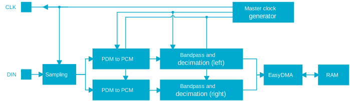
The following figure shows the interaction between the PDM interface and up to two digital microphones. EasyDMA reduces the real-time requirements for controlling the PDM target from a low priority CPU execution context. PDM has the necessary digital filter elements to produce pulse code modulation (PCM) samples and allows continuous audio streaming.
Master clock generator
The PDM clock frequency is adjusted through the PRESCALER register in the master clock. The master clock generator does not add jitter to the selected HFCLK source. It is recommended (but not mandatory) to use the crystal as HFCLK source.
- CLK=PCLK32M/PRESCALER when using PCLK32M
- CLK=ACLK/PRESCALER when using a second CLK source
| Requested PDM frequency fpdm [Hz] | fsource [Hz] | RATIO | PRESCALER | Actual PDM frequency factual [Hz] | Sample frequency [Hz] | Error [%] |
|---|---|---|---|---|---|---|
| 1024000 | 32000000 (PCLK32M) | 64 | 31 | 1032258 | 16129 | 0.8 |
| 1280000 | 32000000 (PCLK32M) | 80 | 25 | 1280000 | 16000 | 0 |
| 800000 | 32000000 (PCLK32M) | 50 | 40 | 800000 | 16000 | 0.0 |
| 1024000 | 24000000 (ACLK) | 64 | 23 | 1043478 | 16304 | 1.9 |
| 1280000 | 24000000 (ACLK) | 80 | 19 | 1263157 | 15789 | -1.31 |
| 800000 | 24000000 (ACLK) | 50 | 30 | 800000 | 16000 | 0.0 |
Module operation
By default, bits from the left PDM microphone are sampled on PDM_CLK falling edge, and bits for the right are sampled on the rising edge of PDM_CLK, resulting in two bitstreams. Each bitstream is fed into a digital filter which converts the PDM stream into 16-bit PCM samples, then filters and down-samples them to reach the appropriate sample rate.
The EDGE field in the MODE register allows swapping left and right channels, so that left will be sampled on rising edge, and right on falling.
The PDM module uses EasyDMA to store the samples coming out from the filters into one buffer in RAM. Depending on the mode chosen in the OPERATION field in the MODE register, memory either contains alternating left and right 16-bit samples (Stereo), or only a left (or only right, depending on the value of the EDGE field) 16-bit samples (Mono). To ensure continuous PDM sampling, it is up to the application to update the EasyDMA destination address pointer as the previous buffer is filled.
The continuous transfer can be started or stopped by sending the START and STOP tasks. STOP becomes effective after the current frame has finished transferring, which will generate the STOPPED event. The STOPPED event indicates that all activity in the module is finished, and that the data is available in RAM (EasyDMA has finished transferring as well). Attempting to restart before receiving the STOPPED event may result in unpredictable behavior.
Soft Gain/Mute
A short description of the Gain, Mute, and Soft Gain/Mute functionality is provided below.
Gain
- GAINL – left channel, in 0.5 dB steps
- GAINR – right channel, in 0.5 dB steps
- FILTER.CTRL.GAINADD0P25 – additional gain, one optional +0.25 dB step that applies to both channels
Custom oversampling rates and CIC filter gain compensation
PDM supports gain compensation, for the selected decimation/oversamling ratio (OSR).
The decimation ratio is set in RATIO, as either one of the listed ratios, or the special value Custom. When RATIO=Custom, the actual decimation rate is configured using the register FILTER.CTRL.DECRATIO. When using custom decimation ratios, configure register FILTER.CTRL.CICFILTERMSBCUSTOM to match FILTER.CTRL.DECRATIO.
PDM uses partial gain compensation towards the closest upper power of 2. For the fixed OSR ratios, compensation gain is fixed and pre-calculated in the design. However, when using custom oversampling ratios, the gain compensation must be calculated and configured.
- Calculate the CIC filter gain:
gainCIC = OSR5
where OSR is the oversampling ratio and the CIC filter order is 5.
- Determine the closest upper power of 2:
closePow2 = floor(log2(gainCIC)) + 1
- Calculate the required gain compensation:
gainComp = -20 × log10(gainCIC / 2closePow2) dB
- Configure the compensation registers:
- FILTER.CTRL.MINORSTEP050CUSTOM – Set the number of +0.5 dB steps
- FILTER.CTRL.MINORSTEP025CUSTOM – To add an additional +0.25 dB step
Mute
The Mute function is a specific case of the Gain function, where the gain coefficient is set to 0.
This function is controlled using the FILTER.SOFTMUTE register.
Soft Gain/Mute
The Soft Gain/Mute provides the possibility to gradually change the gain setting, to avoid a sudden gain change which may lead to audible clicks.
The Soft Gain/Mute function is controlled using the registers FILTER.SOFTCYCLES (the number of soft cycles at the baseband frequency). If FILTER.SOFTCYCLES is set to Custom, then the actual number of softcycles used is configured using the register FILTER.CTRL.SOFTCYCLES (using a multiplication factor of 32).
Gain Range
The desired gain range is [-20, 20]dB with 0.5 dB steps, with the option to improve gain resolution to 0.25 dB steps.
Decimation filter
In order to convert the incoming data stream into PCM audio samples, a decimation filter is included in the PDM peripheral.
The filter input is a two-channel PDM serial stream (with left channel on clock high, right channel on clock low). Output consists of two 16-bit PCM samples at a sample rate lower than the PDM clock rate and a ratio defined by the RATIO register.
A digital volume control is implemented within the filter stage of each channel. It can attenuate or amplify the output samples in a range of ±20 dB of the default (reset) setting and is defined by GPDM,default = 0 dB. The gain is controlled by the GAINL and GAINR registers. As shown in #concept_eqb_fw2_yr__section_vqt_d1g_xcc, depending on OSR value, internal compensation is added for fixed predefined OSR values and a programmable one is available for custom OSR values.
EasyDMA
Samples are written directly to RAM, meaning EasyDMA must be configured appropriately.
The address pointer for the EasyDMA channel is set in the SAMPLE.PTR register. If the destination address set in SAMPLE.PTR is not pointing to the Data RAM region, an EasyDMA transfer may result in a HardFault or RAM corruption. See Memory for more information about memory regions.
DMA transfer supports Stereo (left and right 16-bit samples) and Mono (left only) data transfer as configured in the OPERATION field of the MODE register. The samples are stored as little endian.
| MODE.OPERATION | Bits per sample | Result stored per RAM word | Physical RAM allocated (32-bit words) | Result boundary indexes in RAM | Note |
|---|---|---|---|---|---|
| Stereo | 32 (2x16) | L+R | ceil(SAMPLE.MAXCNT/2) | R0=[31:16] L0=[15:0] | Default |
| Mono | 16 | 2xL | ceil(SAMPLE.MAXCNT/2) | L1=[31:16] L0=[15:0] |
The destination buffer in RAM consists of one block, where the size of the block is set in the SAMPLE.MAXCNT register. The sample format is number of bytes used by the samples that will be stored in the memory. The physical RAM allocated is always the following:
(RAM allocation, in bytes)=SAMPLE.MAXCNT * 2;Sample mapping depends on MODE.OPERATION.
If OPERATION=Stereo, RAM will contain a succession of left and right samples.
If OPERATION=Mono, RAM will contain a succession of left only samples.
For a given value of SAMPLE.MAXCNT, the buffer in RAM can contain half the stereo sampling time as compared to the mono sampling time.
The PDM acquisition can be started by the START task, after the SAMPLE.PTR and SAMPLE.MAXCNT registers have been written. When PDM starts, it will take some time (tPDM,DATA) for the filters to generate valid data. Transients from the PDM microphone itself may also occur. The first few samples (typically around 50) can contain invalid values or transients. It is advised to discard the first few samples after a PDM start.
As soon as the STARTED event is received, the firmware can write the next SAMPLE.PTR value (this register is double-buffered), to ensure continuous operation.
When the buffer in RAM is full of samples, an END event is triggered. The firmware can start processing the data in the buffer. At the same time, PDM starts acquiring data into the new buffer pointed to by SAMPLE.PTR. It sends a new STARTED event, so that the firmware can update SAMPLE.PTR to the next buffer address.
Hardware example
PDM can be configured with a single microphone (mono), or with two microphones.
When a single microphone is used, connect the microphone clock to CLK, and data to DIN. The following figures show a single PDM microphone wired as left.
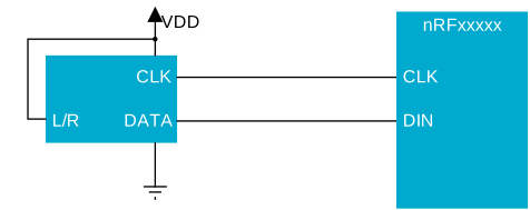
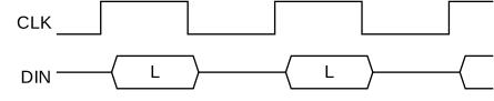
The following figures show a single PDM microphone wired as right.
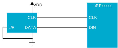
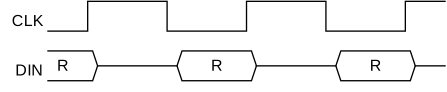
A single microphone (mono) configuration, depending on the microphone’s implementation, either the left or the right channel (sampled at falling or rising CLK edge respectively) will contain reliable data.
If two microphones are used, one of them has to be set as left, the other as right (L/R pin tied high or to GND on the respective microphone). It is strongly recommended to use two identical microphones so their timing in left and right operations match.
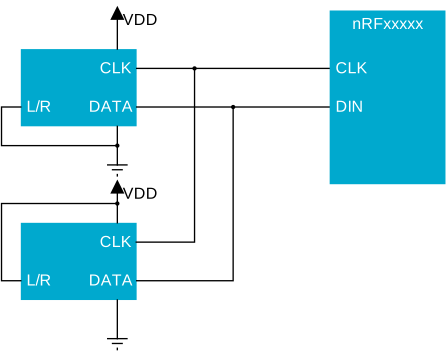
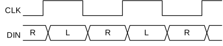
Pin configuration
The CLK and DIN signals assigned to the PDM peripheral are mapped to physical pins according to the configuration specified in the PSEL.CLK and PSEL.DIN registers respectively. If the CONNECT field in any PSEL register is set to Disconnected, the associated PDM signal will not be connected to the required physical pins and will not operate properly.
The PSEL.CLK and PSEL.DIN registers and their configurations are only used when PDM is enabled, and retained while the device is in System ON mode. See POWER — Power control for more information about power modes. When the peripheral is disabled, the pins behave as regular GPIOs, and use the configuration in their respective OUT bit field and PIN_CNF[n] register.
To ensure correct behavior in the PDM module, the pins used by the PDM module must be configured in the GPIO peripheral as described in GPIO configuration before enabling peripheral before enabling the PDM module. This is to ensure that the pins used by the PDM module are driven correctly if the PDM module itself is temporarily disabled or the device temporarily enters System OFF. This configuration must be retained in the GPIO for the selected I/Os as long as the PDM module is supposed to be connected to an external PDM circuit.
Only one peripheral can be assigned to drive a particular GPIO pin at a time. Failing to do so may result in unpredictable behavior.
| PDM signal | PDM pin | Direction | Output value | Comment |
|---|---|---|---|---|
| CLK | As specified in PSEL.CLK | Output | 0 | |
| DIN | As specified in PSEL.DIN | Input | Not applicable |
Registers
Instances
| Instance | Domain | Base address | TrustZone | Split access | Description | ||
|---|---|---|---|---|---|---|---|
| Map | Att | DMA | |||||
PDM20 : S | GLOBAL | 0x500D0000 | US | S | SA | No | Pulse density modulation (digital microphone) interface PDM20 |
PDM21 : S | GLOBAL | 0x500D1000 | US | S | SA | No | Pulse density modulation (digital microphone) interface PDM21 |
Configuration
| Instance | Domain | Configuration |
|---|---|---|
PDM20 : S | GLOBAL | Use GPIO port P1 or P3 ACLK is the fixed 24 MHz clock PCLK24M PCLK is the fixed 32 MHz clock PCLK32M Supports 8, 16, 32, 48 kHz sample rate. CURRENTAMOUNT register included. |
PDM21 : S | GLOBAL | Use GPIO port P1 or P3 ACLK is the fixed 24 MHz clock PCLK24M PCLK is the fixed 32 MHz clock PCLK32M Supports 8, 16, 32, 48 kHz sample rate. CURRENTAMOUNT register included. |
Register overview
| Register | Offset | TZ | Description |
|---|---|---|---|
| TASKS_START | 0x000 | Starts continuous PDM transfer | |
| TASKS_STOP | 0x004 | Stops PDM transfer | |
| SUBSCRIBE_START | 0x080 | Subscribe configuration for task START | |
| SUBSCRIBE_STOP | 0x084 | Subscribe configuration for task STOP | |
| EVENTS_STARTED | 0x100 | PDM transfer has started | |
| EVENTS_STOPPED | 0x104 | PDM transfer has finished | |
| EVENTS_END | 0x108 | The PDM has written the last sample specified by SAMPLE.MAXCNT (or the last sample after a STOP task has been received) to Data RAM | |
| EVENTS_DMA.BUSERROR | 0x110 | This event is generated if an error occurs during the bus transfer. | |
| PUBLISH_STARTED | 0x180 | Publish configuration for event STARTED | |
| PUBLISH_STOPPED | 0x184 | Publish configuration for event STOPPED | |
| PUBLISH_END | 0x188 | Publish configuration for event END | |
| PUBLISH_DMA.BUSERROR | 0x190 | Publish configuration for event DMA.BUSERROR | |
| INTEN | 0x300 | Enable or disable interrupt | |
| INTENSET | 0x304 | Enable interrupt | |
| INTENCLR | 0x308 | Disable interrupt | |
| INTPEND | 0x30C | Pending interrupts | |
| ENABLE | 0x500 | PDM module enable register | |
| MODE | 0x508 | Defines the routing of the connected PDM microphone signals | |
| GAINL | 0x518 | Left output gain adjustment | |
| GAINR | 0x51C | Right output gain adjustment | |
| RATIO | 0x520 | Selects the decimation ratio between PDM_CLK and output sample rate. When RATIO is selected to be "custom", the decimation rate should be set using the FILTER.CTRL field before setting the RATIO to 7 Change PRESCALER.DIVISOR accordingly. | |
| FILTER.CTRL | 0x524 | Aditional PDM configurability | |
| FILTER.HPPOLE | 0x528 | Settings for the high-pass filter | |
| FILTER.HPDISABLE | 0x52C | High pass filter disable | |
| FILTER.SOFTMUTE | 0x530 | Soft mute function | |
| FILTER.SOFTCYCLES | 0x534 | Soft mute settings | |
| FILTER.SAMPLEDELAY | 0x538 | Input Data Sampling with Number of ckFilterL (double frequency of PDM_CLK) Clock Cycle Delay. Optionally,input sample point can be delayed independently on left and right channels using FILTER:CTRL[20:19] bits | |
| PSEL.CLK | 0x540 | Pin number configuration for PDM CLK signal | |
| PSEL.DIN | 0x544 | Pin number configuration for PDM DIN signal | |
| CLKSELECT | 0x54C | Master clock generator configuration | |
| SAMPLE.PTR | 0x560 | RAM address pointer to write samples to with EasyDMA | |
| SAMPLE.MAXCNT | 0x564 | Number of bytes to allocate memory for in EasyDMA mode | |
| PRESCALER | 0x580 | The prescaler is used to set the PDM frequency | |
| DMA.TERMINATEONBUSERROR | 0x700 | Terminate the transaction if a BUSERROR event is detected. | |
| DMA.BUSERRORADDRESS | 0x704 | Address of transaction that generated the last BUSERROR event. |
TASKS_START
Address offset: 0x000
Starts continuous PDM transfer
| Bit number | 31 | 30 | 29 | 28 | 27 | 26 | 25 | 24 | 23 | 22 | 21 | 20 | 19 | 18 | 17 | 16 | 15 | 14 | 13 | 12 | 11 | 10 | 9 | 8 | 7 | 6 | 5 | 4 | 3 | 2 | 1 | 0 | |||
|---|---|---|---|---|---|---|---|---|---|---|---|---|---|---|---|---|---|---|---|---|---|---|---|---|---|---|---|---|---|---|---|---|---|---|---|
| ID | A | ||||||||||||||||||||||||||||||||||
| Reset 0x00000000 | 0 | 0 | 0 | 0 | 0 | 0 | 0 | 0 | 0 | 0 | 0 | 0 | 0 | 0 | 0 | 0 | 0 | 0 | 0 | 0 | 0 | 0 | 0 | 0 | 0 | 0 | 0 | 0 | 0 | 0 | 0 | 0 | |||
| ID | R/W | Field | Value ID | Value | Description | ||||||||||||||||||||||||||||||
| A | W | TASKS_START | Starts continuous PDM transfer | ||||||||||||||||||||||||||||||||
Trigger | 1 | Trigger task | |||||||||||||||||||||||||||||||||
TASKS_STOP
Address offset: 0x004
Stops PDM transfer
| Bit number | 31 | 30 | 29 | 28 | 27 | 26 | 25 | 24 | 23 | 22 | 21 | 20 | 19 | 18 | 17 | 16 | 15 | 14 | 13 | 12 | 11 | 10 | 9 | 8 | 7 | 6 | 5 | 4 | 3 | 2 | 1 | 0 | |||
|---|---|---|---|---|---|---|---|---|---|---|---|---|---|---|---|---|---|---|---|---|---|---|---|---|---|---|---|---|---|---|---|---|---|---|---|
| ID | A | ||||||||||||||||||||||||||||||||||
| Reset 0x00000000 | 0 | 0 | 0 | 0 | 0 | 0 | 0 | 0 | 0 | 0 | 0 | 0 | 0 | 0 | 0 | 0 | 0 | 0 | 0 | 0 | 0 | 0 | 0 | 0 | 0 | 0 | 0 | 0 | 0 | 0 | 0 | 0 | |||
| ID | R/W | Field | Value ID | Value | Description | ||||||||||||||||||||||||||||||
| A | W | TASKS_STOP | Stops PDM transfer | ||||||||||||||||||||||||||||||||
Trigger | 1 | Trigger task | |||||||||||||||||||||||||||||||||
SUBSCRIBE_START
Address offset: 0x080
Subscribe configuration for task START
| Bit number | 31 | 30 | 29 | 28 | 27 | 26 | 25 | 24 | 23 | 22 | 21 | 20 | 19 | 18 | 17 | 16 | 15 | 14 | 13 | 12 | 11 | 10 | 9 | 8 | 7 | 6 | 5 | 4 | 3 | 2 | 1 | 0 | |||
|---|---|---|---|---|---|---|---|---|---|---|---|---|---|---|---|---|---|---|---|---|---|---|---|---|---|---|---|---|---|---|---|---|---|---|---|
| ID | B | A | A | A | A | A | A | A | A | ||||||||||||||||||||||||||
| Reset 0x00000000 | 0 | 0 | 0 | 0 | 0 | 0 | 0 | 0 | 0 | 0 | 0 | 0 | 0 | 0 | 0 | 0 | 0 | 0 | 0 | 0 | 0 | 0 | 0 | 0 | 0 | 0 | 0 | 0 | 0 | 0 | 0 | 0 | |||
| ID | R/W | Field | Value ID | Value | Description | ||||||||||||||||||||||||||||||
| A | RW | CHIDX | [0..255] | DPPI channel that task START will subscribe to | |||||||||||||||||||||||||||||||
| B | RW | EN | |||||||||||||||||||||||||||||||||
Disabled | 0 | Disable subscription | |||||||||||||||||||||||||||||||||
Enabled | 1 | Enable subscription | |||||||||||||||||||||||||||||||||
SUBSCRIBE_STOP
Address offset: 0x084
Subscribe configuration for task STOP
| Bit number | 31 | 30 | 29 | 28 | 27 | 26 | 25 | 24 | 23 | 22 | 21 | 20 | 19 | 18 | 17 | 16 | 15 | 14 | 13 | 12 | 11 | 10 | 9 | 8 | 7 | 6 | 5 | 4 | 3 | 2 | 1 | 0 | |||
|---|---|---|---|---|---|---|---|---|---|---|---|---|---|---|---|---|---|---|---|---|---|---|---|---|---|---|---|---|---|---|---|---|---|---|---|
| ID | B | A | A | A | A | A | A | A | A | ||||||||||||||||||||||||||
| Reset 0x00000000 | 0 | 0 | 0 | 0 | 0 | 0 | 0 | 0 | 0 | 0 | 0 | 0 | 0 | 0 | 0 | 0 | 0 | 0 | 0 | 0 | 0 | 0 | 0 | 0 | 0 | 0 | 0 | 0 | 0 | 0 | 0 | 0 | |||
| ID | R/W | Field | Value ID | Value | Description | ||||||||||||||||||||||||||||||
| A | RW | CHIDX | [0..255] | DPPI channel that task STOP will subscribe to | |||||||||||||||||||||||||||||||
| B | RW | EN | |||||||||||||||||||||||||||||||||
Disabled | 0 | Disable subscription | |||||||||||||||||||||||||||||||||
Enabled | 1 | Enable subscription | |||||||||||||||||||||||||||||||||
EVENTS_STARTED
Address offset: 0x100
PDM transfer has started
| Bit number | 31 | 30 | 29 | 28 | 27 | 26 | 25 | 24 | 23 | 22 | 21 | 20 | 19 | 18 | 17 | 16 | 15 | 14 | 13 | 12 | 11 | 10 | 9 | 8 | 7 | 6 | 5 | 4 | 3 | 2 | 1 | 0 | |||
|---|---|---|---|---|---|---|---|---|---|---|---|---|---|---|---|---|---|---|---|---|---|---|---|---|---|---|---|---|---|---|---|---|---|---|---|
| ID | A | ||||||||||||||||||||||||||||||||||
| Reset 0x00000000 | 0 | 0 | 0 | 0 | 0 | 0 | 0 | 0 | 0 | 0 | 0 | 0 | 0 | 0 | 0 | 0 | 0 | 0 | 0 | 0 | 0 | 0 | 0 | 0 | 0 | 0 | 0 | 0 | 0 | 0 | 0 | 0 | |||
| ID | R/W | Field | Value ID | Value | Description | ||||||||||||||||||||||||||||||
| A | RW | EVENTS_STARTED | PDM transfer has started | ||||||||||||||||||||||||||||||||
NotGenerated | 0 | Event not generated | |||||||||||||||||||||||||||||||||
Generated | 1 | Event generated | |||||||||||||||||||||||||||||||||
EVENTS_STOPPED
Address offset: 0x104
PDM transfer has finished
| Bit number | 31 | 30 | 29 | 28 | 27 | 26 | 25 | 24 | 23 | 22 | 21 | 20 | 19 | 18 | 17 | 16 | 15 | 14 | 13 | 12 | 11 | 10 | 9 | 8 | 7 | 6 | 5 | 4 | 3 | 2 | 1 | 0 | |||
|---|---|---|---|---|---|---|---|---|---|---|---|---|---|---|---|---|---|---|---|---|---|---|---|---|---|---|---|---|---|---|---|---|---|---|---|
| ID | A | ||||||||||||||||||||||||||||||||||
| Reset 0x00000000 | 0 | 0 | 0 | 0 | 0 | 0 | 0 | 0 | 0 | 0 | 0 | 0 | 0 | 0 | 0 | 0 | 0 | 0 | 0 | 0 | 0 | 0 | 0 | 0 | 0 | 0 | 0 | 0 | 0 | 0 | 0 | 0 | |||
| ID | R/W | Field | Value ID | Value | Description | ||||||||||||||||||||||||||||||
| A | RW | EVENTS_STOPPED | PDM transfer has finished | ||||||||||||||||||||||||||||||||
NotGenerated | 0 | Event not generated | |||||||||||||||||||||||||||||||||
Generated | 1 | Event generated | |||||||||||||||||||||||||||||||||
EVENTS_END
Address offset: 0x108
The PDM has written the last sample specified by SAMPLE.MAXCNT (or the last sample after a STOP task has been received) to Data RAM
| Bit number | 31 | 30 | 29 | 28 | 27 | 26 | 25 | 24 | 23 | 22 | 21 | 20 | 19 | 18 | 17 | 16 | 15 | 14 | 13 | 12 | 11 | 10 | 9 | 8 | 7 | 6 | 5 | 4 | 3 | 2 | 1 | 0 | |||
|---|---|---|---|---|---|---|---|---|---|---|---|---|---|---|---|---|---|---|---|---|---|---|---|---|---|---|---|---|---|---|---|---|---|---|---|
| ID | A | ||||||||||||||||||||||||||||||||||
| Reset 0x00000000 | 0 | 0 | 0 | 0 | 0 | 0 | 0 | 0 | 0 | 0 | 0 | 0 | 0 | 0 | 0 | 0 | 0 | 0 | 0 | 0 | 0 | 0 | 0 | 0 | 0 | 0 | 0 | 0 | 0 | 0 | 0 | 0 | |||
| ID | R/W | Field | Value ID | Value | Description | ||||||||||||||||||||||||||||||
| A | RW | EVENTS_END | The PDM has written the last sample specified by SAMPLE.MAXCNT (or the last sample after a STOP task has been received) to Data RAM | ||||||||||||||||||||||||||||||||
NotGenerated | 0 | Event not generated | |||||||||||||||||||||||||||||||||
Generated | 1 | Event generated | |||||||||||||||||||||||||||||||||
EVENTS_DMA
Peripheral events.
EVENTS_DMA.BUSERROR
Address offset: 0x110
This event is generated if an error occurs during the bus transfer.
When this event is generated, the address which caused the error can be read from the BUSERRORADDRESS register.
Errors occurring while the EVENTS_BUSERROR register is set are ignored.
| Bit number | 31 | 30 | 29 | 28 | 27 | 26 | 25 | 24 | 23 | 22 | 21 | 20 | 19 | 18 | 17 | 16 | 15 | 14 | 13 | 12 | 11 | 10 | 9 | 8 | 7 | 6 | 5 | 4 | 3 | 2 | 1 | 0 | |||
|---|---|---|---|---|---|---|---|---|---|---|---|---|---|---|---|---|---|---|---|---|---|---|---|---|---|---|---|---|---|---|---|---|---|---|---|
| ID | A | ||||||||||||||||||||||||||||||||||
| Reset 0x00000000 | 0 | 0 | 0 | 0 | 0 | 0 | 0 | 0 | 0 | 0 | 0 | 0 | 0 | 0 | 0 | 0 | 0 | 0 | 0 | 0 | 0 | 0 | 0 | 0 | 0 | 0 | 0 | 0 | 0 | 0 | 0 | 0 | |||
| ID | R/W | Field | Value ID | Value | Description | ||||||||||||||||||||||||||||||
| A | RW | BUSERROR | This event is generated if an error occurs during the bus transfer. When this event is generated, the address which caused the error can be read from the BUSERRORADDRESS register. Errors occurring while the EVENTS_BUSERROR register is set are ignored. | ||||||||||||||||||||||||||||||||
NotGenerated | 0 | Event not generated | |||||||||||||||||||||||||||||||||
Generated | 1 | Event generated | |||||||||||||||||||||||||||||||||
PUBLISH_STARTED
Address offset: 0x180
Publish configuration for event STARTED
| Bit number | 31 | 30 | 29 | 28 | 27 | 26 | 25 | 24 | 23 | 22 | 21 | 20 | 19 | 18 | 17 | 16 | 15 | 14 | 13 | 12 | 11 | 10 | 9 | 8 | 7 | 6 | 5 | 4 | 3 | 2 | 1 | 0 | |||
|---|---|---|---|---|---|---|---|---|---|---|---|---|---|---|---|---|---|---|---|---|---|---|---|---|---|---|---|---|---|---|---|---|---|---|---|
| ID | B | A | A | A | A | A | A | A | A | ||||||||||||||||||||||||||
| Reset 0x00000000 | 0 | 0 | 0 | 0 | 0 | 0 | 0 | 0 | 0 | 0 | 0 | 0 | 0 | 0 | 0 | 0 | 0 | 0 | 0 | 0 | 0 | 0 | 0 | 0 | 0 | 0 | 0 | 0 | 0 | 0 | 0 | 0 | |||
| ID | R/W | Field | Value ID | Value | Description | ||||||||||||||||||||||||||||||
| A | RW | CHIDX | [0..255] | DPPI channel that event STARTED will publish to | |||||||||||||||||||||||||||||||
| B | RW | EN | |||||||||||||||||||||||||||||||||
Disabled | 0 | Disable publishing | |||||||||||||||||||||||||||||||||
Enabled | 1 | Enable publishing | |||||||||||||||||||||||||||||||||
PUBLISH_STOPPED
Address offset: 0x184
Publish configuration for event STOPPED
| Bit number | 31 | 30 | 29 | 28 | 27 | 26 | 25 | 24 | 23 | 22 | 21 | 20 | 19 | 18 | 17 | 16 | 15 | 14 | 13 | 12 | 11 | 10 | 9 | 8 | 7 | 6 | 5 | 4 | 3 | 2 | 1 | 0 | |||
|---|---|---|---|---|---|---|---|---|---|---|---|---|---|---|---|---|---|---|---|---|---|---|---|---|---|---|---|---|---|---|---|---|---|---|---|
| ID | B | A | A | A | A | A | A | A | A | ||||||||||||||||||||||||||
| Reset 0x00000000 | 0 | 0 | 0 | 0 | 0 | 0 | 0 | 0 | 0 | 0 | 0 | 0 | 0 | 0 | 0 | 0 | 0 | 0 | 0 | 0 | 0 | 0 | 0 | 0 | 0 | 0 | 0 | 0 | 0 | 0 | 0 | 0 | |||
| ID | R/W | Field | Value ID | Value | Description | ||||||||||||||||||||||||||||||
| A | RW | CHIDX | [0..255] | DPPI channel that event STOPPED will publish to | |||||||||||||||||||||||||||||||
| B | RW | EN | |||||||||||||||||||||||||||||||||
Disabled | 0 | Disable publishing | |||||||||||||||||||||||||||||||||
Enabled | 1 | Enable publishing | |||||||||||||||||||||||||||||||||
PUBLISH_END
Address offset: 0x188
Publish configuration for event END
| Bit number | 31 | 30 | 29 | 28 | 27 | 26 | 25 | 24 | 23 | 22 | 21 | 20 | 19 | 18 | 17 | 16 | 15 | 14 | 13 | 12 | 11 | 10 | 9 | 8 | 7 | 6 | 5 | 4 | 3 | 2 | 1 | 0 | |||
|---|---|---|---|---|---|---|---|---|---|---|---|---|---|---|---|---|---|---|---|---|---|---|---|---|---|---|---|---|---|---|---|---|---|---|---|
| ID | B | A | A | A | A | A | A | A | A | ||||||||||||||||||||||||||
| Reset 0x00000000 | 0 | 0 | 0 | 0 | 0 | 0 | 0 | 0 | 0 | 0 | 0 | 0 | 0 | 0 | 0 | 0 | 0 | 0 | 0 | 0 | 0 | 0 | 0 | 0 | 0 | 0 | 0 | 0 | 0 | 0 | 0 | 0 | |||
| ID | R/W | Field | Value ID | Value | Description | ||||||||||||||||||||||||||||||
| A | RW | CHIDX | [0..255] | DPPI channel that event END will publish to | |||||||||||||||||||||||||||||||
| B | RW | EN | |||||||||||||||||||||||||||||||||
Disabled | 0 | Disable publishing | |||||||||||||||||||||||||||||||||
Enabled | 1 | Enable publishing | |||||||||||||||||||||||||||||||||
PUBLISH_DMA
Publish configuration for events
PUBLISH_DMA.BUSERROR
Address offset: 0x190
Publish configuration for event DMA.BUSERROR
When this event is generated, the address which caused the error can be read from the BUSERRORADDRESS register.
Errors occurring while the EVENTS_BUSERROR register is set are ignored.
| Bit number | 31 | 30 | 29 | 28 | 27 | 26 | 25 | 24 | 23 | 22 | 21 | 20 | 19 | 18 | 17 | 16 | 15 | 14 | 13 | 12 | 11 | 10 | 9 | 8 | 7 | 6 | 5 | 4 | 3 | 2 | 1 | 0 | |||
|---|---|---|---|---|---|---|---|---|---|---|---|---|---|---|---|---|---|---|---|---|---|---|---|---|---|---|---|---|---|---|---|---|---|---|---|
| ID | B | A | A | A | A | A | A | A | A | ||||||||||||||||||||||||||
| Reset 0x00000000 | 0 | 0 | 0 | 0 | 0 | 0 | 0 | 0 | 0 | 0 | 0 | 0 | 0 | 0 | 0 | 0 | 0 | 0 | 0 | 0 | 0 | 0 | 0 | 0 | 0 | 0 | 0 | 0 | 0 | 0 | 0 | 0 | |||
| ID | R/W | Field | Value ID | Value | Description | ||||||||||||||||||||||||||||||
| A | RW | CHIDX | [0..255] | DPPI channel that event DMA.BUSERROR will publish to | |||||||||||||||||||||||||||||||
| B | RW | EN | |||||||||||||||||||||||||||||||||
Disabled | 0 | Disable publishing | |||||||||||||||||||||||||||||||||
Enabled | 1 | Enable publishing | |||||||||||||||||||||||||||||||||
INTEN
Address offset: 0x300
Enable or disable interrupt
| Bit number | 31 | 30 | 29 | 28 | 27 | 26 | 25 | 24 | 23 | 22 | 21 | 20 | 19 | 18 | 17 | 16 | 15 | 14 | 13 | 12 | 11 | 10 | 9 | 8 | 7 | 6 | 5 | 4 | 3 | 2 | 1 | 0 | |||
|---|---|---|---|---|---|---|---|---|---|---|---|---|---|---|---|---|---|---|---|---|---|---|---|---|---|---|---|---|---|---|---|---|---|---|---|
| ID | D | C | B | A | |||||||||||||||||||||||||||||||
| Reset 0x00000000 | 0 | 0 | 0 | 0 | 0 | 0 | 0 | 0 | 0 | 0 | 0 | 0 | 0 | 0 | 0 | 0 | 0 | 0 | 0 | 0 | 0 | 0 | 0 | 0 | 0 | 0 | 0 | 0 | 0 | 0 | 0 | 0 | |||
| ID | R/W | Field | Value ID | Value | Description | ||||||||||||||||||||||||||||||
| A | RW | STARTED | Enable or disable interrupt for event STARTED | ||||||||||||||||||||||||||||||||
Disabled | 0 | Disable | |||||||||||||||||||||||||||||||||
Enabled | 1 | Enable | |||||||||||||||||||||||||||||||||
| B | RW | STOPPED | Enable or disable interrupt for event STOPPED | ||||||||||||||||||||||||||||||||
Disabled | 0 | Disable | |||||||||||||||||||||||||||||||||
Enabled | 1 | Enable | |||||||||||||||||||||||||||||||||
| C | RW | END | Enable or disable interrupt for event END | ||||||||||||||||||||||||||||||||
Disabled | 0 | Disable | |||||||||||||||||||||||||||||||||
Enabled | 1 | Enable | |||||||||||||||||||||||||||||||||
| D | RW | DMABUSERROR | Enable or disable interrupt for event DMABUSERROR When this event is generated, the address which caused the error can be read from the BUSERRORADDRESS register. Errors occurring while the EVENTS_BUSERROR register is set are ignored. | ||||||||||||||||||||||||||||||||
Disabled | 0 | Disable | |||||||||||||||||||||||||||||||||
Enabled | 1 | Enable | |||||||||||||||||||||||||||||||||
INTENSET
Address offset: 0x304
Enable interrupt
| Bit number | 31 | 30 | 29 | 28 | 27 | 26 | 25 | 24 | 23 | 22 | 21 | 20 | 19 | 18 | 17 | 16 | 15 | 14 | 13 | 12 | 11 | 10 | 9 | 8 | 7 | 6 | 5 | 4 | 3 | 2 | 1 | 0 | |||
|---|---|---|---|---|---|---|---|---|---|---|---|---|---|---|---|---|---|---|---|---|---|---|---|---|---|---|---|---|---|---|---|---|---|---|---|
| ID | D | C | B | A | |||||||||||||||||||||||||||||||
| Reset 0x00000000 | 0 | 0 | 0 | 0 | 0 | 0 | 0 | 0 | 0 | 0 | 0 | 0 | 0 | 0 | 0 | 0 | 0 | 0 | 0 | 0 | 0 | 0 | 0 | 0 | 0 | 0 | 0 | 0 | 0 | 0 | 0 | 0 | |||
| ID | R/W | Field | Value ID | Value | Description | ||||||||||||||||||||||||||||||
| A | RW | STARTED | Write '1' to enable interrupt for event STARTED | ||||||||||||||||||||||||||||||||
Set | 1 | Enable | |||||||||||||||||||||||||||||||||
Disabled | 0 | Read: Disabled | |||||||||||||||||||||||||||||||||
Enabled | 1 | Read: Enabled | |||||||||||||||||||||||||||||||||
| B | RW | STOPPED | Write '1' to enable interrupt for event STOPPED | ||||||||||||||||||||||||||||||||
Set | 1 | Enable | |||||||||||||||||||||||||||||||||
Disabled | 0 | Read: Disabled | |||||||||||||||||||||||||||||||||
Enabled | 1 | Read: Enabled | |||||||||||||||||||||||||||||||||
| C | RW | END | Write '1' to enable interrupt for event END | ||||||||||||||||||||||||||||||||
Set | 1 | Enable | |||||||||||||||||||||||||||||||||
Disabled | 0 | Read: Disabled | |||||||||||||||||||||||||||||||||
Enabled | 1 | Read: Enabled | |||||||||||||||||||||||||||||||||
| D | RW | DMABUSERROR | Write '1' to enable interrupt for event DMABUSERROR When this event is generated, the address which caused the error can be read from the BUSERRORADDRESS register. Errors occurring while the EVENTS_BUSERROR register is set are ignored. | ||||||||||||||||||||||||||||||||
Set | 1 | Enable | |||||||||||||||||||||||||||||||||
Disabled | 0 | Read: Disabled | |||||||||||||||||||||||||||||||||
Enabled | 1 | Read: Enabled | |||||||||||||||||||||||||||||||||
INTENCLR
Address offset: 0x308
Disable interrupt
| Bit number | 31 | 30 | 29 | 28 | 27 | 26 | 25 | 24 | 23 | 22 | 21 | 20 | 19 | 18 | 17 | 16 | 15 | 14 | 13 | 12 | 11 | 10 | 9 | 8 | 7 | 6 | 5 | 4 | 3 | 2 | 1 | 0 | |||
|---|---|---|---|---|---|---|---|---|---|---|---|---|---|---|---|---|---|---|---|---|---|---|---|---|---|---|---|---|---|---|---|---|---|---|---|
| ID | D | C | B | A | |||||||||||||||||||||||||||||||
| Reset 0x00000000 | 0 | 0 | 0 | 0 | 0 | 0 | 0 | 0 | 0 | 0 | 0 | 0 | 0 | 0 | 0 | 0 | 0 | 0 | 0 | 0 | 0 | 0 | 0 | 0 | 0 | 0 | 0 | 0 | 0 | 0 | 0 | 0 | |||
| ID | R/W | Field | Value ID | Value | Description | ||||||||||||||||||||||||||||||
| A | RW | STARTED | Write '1' to disable interrupt for event STARTED | ||||||||||||||||||||||||||||||||
Clear | 1 | Disable | |||||||||||||||||||||||||||||||||
Disabled | 0 | Read: Disabled | |||||||||||||||||||||||||||||||||
Enabled | 1 | Read: Enabled | |||||||||||||||||||||||||||||||||
| B | RW | STOPPED | Write '1' to disable interrupt for event STOPPED | ||||||||||||||||||||||||||||||||
Clear | 1 | Disable | |||||||||||||||||||||||||||||||||
Disabled | 0 | Read: Disabled | |||||||||||||||||||||||||||||||||
Enabled | 1 | Read: Enabled | |||||||||||||||||||||||||||||||||
| C | RW | END | Write '1' to disable interrupt for event END | ||||||||||||||||||||||||||||||||
Clear | 1 | Disable | |||||||||||||||||||||||||||||||||
Disabled | 0 | Read: Disabled | |||||||||||||||||||||||||||||||||
Enabled | 1 | Read: Enabled | |||||||||||||||||||||||||||||||||
| D | RW | DMABUSERROR | Write '1' to disable interrupt for event DMABUSERROR When this event is generated, the address which caused the error can be read from the BUSERRORADDRESS register. Errors occurring while the EVENTS_BUSERROR register is set are ignored. | ||||||||||||||||||||||||||||||||
Clear | 1 | Disable | |||||||||||||||||||||||||||||||||
Disabled | 0 | Read: Disabled | |||||||||||||||||||||||||||||||||
Enabled | 1 | Read: Enabled | |||||||||||||||||||||||||||||||||
INTPEND
Address offset: 0x30C
Pending interrupts
| Bit number | 31 | 30 | 29 | 28 | 27 | 26 | 25 | 24 | 23 | 22 | 21 | 20 | 19 | 18 | 17 | 16 | 15 | 14 | 13 | 12 | 11 | 10 | 9 | 8 | 7 | 6 | 5 | 4 | 3 | 2 | 1 | 0 | |||
|---|---|---|---|---|---|---|---|---|---|---|---|---|---|---|---|---|---|---|---|---|---|---|---|---|---|---|---|---|---|---|---|---|---|---|---|
| ID | D | C | B | A | |||||||||||||||||||||||||||||||
| Reset 0x00000000 | 0 | 0 | 0 | 0 | 0 | 0 | 0 | 0 | 0 | 0 | 0 | 0 | 0 | 0 | 0 | 0 | 0 | 0 | 0 | 0 | 0 | 0 | 0 | 0 | 0 | 0 | 0 | 0 | 0 | 0 | 0 | 0 | |||
| ID | R/W | Field | Value ID | Value | Description | ||||||||||||||||||||||||||||||
| A | R | STARTED | Read pending status of interrupt for event STARTED | ||||||||||||||||||||||||||||||||
NotPending | 0 | Read: Not pending | |||||||||||||||||||||||||||||||||
Pending | 1 | Read: Pending | |||||||||||||||||||||||||||||||||
| B | R | STOPPED | Read pending status of interrupt for event STOPPED | ||||||||||||||||||||||||||||||||
NotPending | 0 | Read: Not pending | |||||||||||||||||||||||||||||||||
Pending | 1 | Read: Pending | |||||||||||||||||||||||||||||||||
| C | R | END | Read pending status of interrupt for event END | ||||||||||||||||||||||||||||||||
NotPending | 0 | Read: Not pending | |||||||||||||||||||||||||||||||||
Pending | 1 | Read: Pending | |||||||||||||||||||||||||||||||||
| D | R | DMABUSERROR | Read pending status of interrupt for event DMABUSERROR When this event is generated, the address which caused the error can be read from the BUSERRORADDRESS register. Errors occurring while the EVENTS_BUSERROR register is set are ignored. | ||||||||||||||||||||||||||||||||
NotPending | 0 | Read: Not pending | |||||||||||||||||||||||||||||||||
Pending | 1 | Read: Pending | |||||||||||||||||||||||||||||||||
ENABLE
Address offset: 0x500
PDM module enable register
| Bit number | 31 | 30 | 29 | 28 | 27 | 26 | 25 | 24 | 23 | 22 | 21 | 20 | 19 | 18 | 17 | 16 | 15 | 14 | 13 | 12 | 11 | 10 | 9 | 8 | 7 | 6 | 5 | 4 | 3 | 2 | 1 | 0 | |||
|---|---|---|---|---|---|---|---|---|---|---|---|---|---|---|---|---|---|---|---|---|---|---|---|---|---|---|---|---|---|---|---|---|---|---|---|
| ID | A | ||||||||||||||||||||||||||||||||||
| Reset 0x00000000 | 0 | 0 | 0 | 0 | 0 | 0 | 0 | 0 | 0 | 0 | 0 | 0 | 0 | 0 | 0 | 0 | 0 | 0 | 0 | 0 | 0 | 0 | 0 | 0 | 0 | 0 | 0 | 0 | 0 | 0 | 0 | 0 | |||
| ID | R/W | Field | Value ID | Value | Description | ||||||||||||||||||||||||||||||
| A | RW | ENABLE | Enable or disable PDM module | ||||||||||||||||||||||||||||||||
Disabled | 0 | Disable | |||||||||||||||||||||||||||||||||
Enabled | 1 | Enable | |||||||||||||||||||||||||||||||||
MODE
Address offset: 0x508
Defines the routing of the connected PDM microphone signals
| Bit number | 31 | 30 | 29 | 28 | 27 | 26 | 25 | 24 | 23 | 22 | 21 | 20 | 19 | 18 | 17 | 16 | 15 | 14 | 13 | 12 | 11 | 10 | 9 | 8 | 7 | 6 | 5 | 4 | 3 | 2 | 1 | 0 | |||
|---|---|---|---|---|---|---|---|---|---|---|---|---|---|---|---|---|---|---|---|---|---|---|---|---|---|---|---|---|---|---|---|---|---|---|---|
| ID | B | A | |||||||||||||||||||||||||||||||||
| Reset 0x00000000 | 0 | 0 | 0 | 0 | 0 | 0 | 0 | 0 | 0 | 0 | 0 | 0 | 0 | 0 | 0 | 0 | 0 | 0 | 0 | 0 | 0 | 0 | 0 | 0 | 0 | 0 | 0 | 0 | 0 | 0 | 0 | 0 | |||
| ID | R/W | Field | Value ID | Value | Description | ||||||||||||||||||||||||||||||
| A | RW | OPERATION | Mono or stereo operation | ||||||||||||||||||||||||||||||||
Stereo | 0 | Sample and store one pair (left + right) of 16-bit samples per RAM word R=[31:16]; L=[15:0] | |||||||||||||||||||||||||||||||||
Mono | 1 | Sample and store two successive left samples (16 bits each) per RAM word L1=[31:16]; L0=[15:0] | |||||||||||||||||||||||||||||||||
| B | RW | EDGE | Defines on which PDM_CLK edge left (or mono) is sampled. The right channel is sampled on the opposide edge of the left channel. When EDGE is set to 1 (LeftRising) and stereo input is used the right and left channels are swapped relative to EDGE set to 0 (LeftFalling). | ||||||||||||||||||||||||||||||||
LeftFalling | 0 | Left (or mono) is sampled on falling edge of PDM_CLK | |||||||||||||||||||||||||||||||||
LeftRising | 1 | Left (or mono) is sampled on rising edge of PDM_CLK | |||||||||||||||||||||||||||||||||
GAINL
Address offset: 0x518
Left output gain adjustment
| Bit number | 31 | 30 | 29 | 28 | 27 | 26 | 25 | 24 | 23 | 22 | 21 | 20 | 19 | 18 | 17 | 16 | 15 | 14 | 13 | 12 | 11 | 10 | 9 | 8 | 7 | 6 | 5 | 4 | 3 | 2 | 1 | 0 | |||
|---|---|---|---|---|---|---|---|---|---|---|---|---|---|---|---|---|---|---|---|---|---|---|---|---|---|---|---|---|---|---|---|---|---|---|---|
| ID | A | A | A | A | A | A | A | ||||||||||||||||||||||||||||
| Reset 0x00000028 | 0 | 0 | 0 | 0 | 0 | 0 | 0 | 0 | 0 | 0 | 0 | 0 | 0 | 0 | 0 | 0 | 0 | 0 | 0 | 0 | 0 | 0 | 0 | 0 | 0 | 0 | 1 | 0 | 1 | 0 | 0 | 0 | |||
| ID | R/W | Field | Value ID | Value | Description | ||||||||||||||||||||||||||||||
| A | RW | GAINL | Left output gain adjustment, in 0.5 dB steps, around the default module gain (see electrical parameters) 0x00 -20 dB gain adjust 0x01 -19.5 dB gain adjust (...) 0x27 -0.5 dB gain adjust 0x28 0 dB gain adjust 0x29 +0.5 dB gain adjust (...) 0x4F +19.5 dB gain adjust 0x50 +20 dB gain adjust | ||||||||||||||||||||||||||||||||
MinGain | 0x00 | -20 dB gain adjustment (minimum) | |||||||||||||||||||||||||||||||||
DefaultGain | 0x28 | 0 dB gain adjustment | |||||||||||||||||||||||||||||||||
MaxGain | 0x50 | +20 dB gain adjustment (maximum) | |||||||||||||||||||||||||||||||||
GAINR
Address offset: 0x51C
Right output gain adjustment
| Bit number | 31 | 30 | 29 | 28 | 27 | 26 | 25 | 24 | 23 | 22 | 21 | 20 | 19 | 18 | 17 | 16 | 15 | 14 | 13 | 12 | 11 | 10 | 9 | 8 | 7 | 6 | 5 | 4 | 3 | 2 | 1 | 0 | |||
|---|---|---|---|---|---|---|---|---|---|---|---|---|---|---|---|---|---|---|---|---|---|---|---|---|---|---|---|---|---|---|---|---|---|---|---|
| ID | A | A | A | A | A | A | A | ||||||||||||||||||||||||||||
| Reset 0x00000028 | 0 | 0 | 0 | 0 | 0 | 0 | 0 | 0 | 0 | 0 | 0 | 0 | 0 | 0 | 0 | 0 | 0 | 0 | 0 | 0 | 0 | 0 | 0 | 0 | 0 | 0 | 1 | 0 | 1 | 0 | 0 | 0 | |||
| ID | R/W | Field | Value ID | Value | Description | ||||||||||||||||||||||||||||||
| A | RW | GAINR | Right output gain adjustment, in 0.5 dB steps, around the default module gain (see electrical parameters) | ||||||||||||||||||||||||||||||||
MinGain | 0x00 | -20 dB gain adjustment (minimum) | |||||||||||||||||||||||||||||||||
DefaultGain | 0x28 | 0 dB gain adjustment | |||||||||||||||||||||||||||||||||
MaxGain | 0x50 | +20 dB gain adjustment (maximum) | |||||||||||||||||||||||||||||||||
RATIO
Address offset: 0x520
Selects the decimation ratio between PDM_CLK and output sample rate. When RATIO is selected to be "custom", the decimation rate should be set using the FILTER.CTRL field before setting the RATIO to 7
Change PRESCALER.DIVISOR accordingly.
| Bit number | 31 | 30 | 29 | 28 | 27 | 26 | 25 | 24 | 23 | 22 | 21 | 20 | 19 | 18 | 17 | 16 | 15 | 14 | 13 | 12 | 11 | 10 | 9 | 8 | 7 | 6 | 5 | 4 | 3 | 2 | 1 | 0 | |||
|---|---|---|---|---|---|---|---|---|---|---|---|---|---|---|---|---|---|---|---|---|---|---|---|---|---|---|---|---|---|---|---|---|---|---|---|
| ID | A | A | A | ||||||||||||||||||||||||||||||||
| Reset 0x00000002 | 0 | 0 | 0 | 0 | 0 | 0 | 0 | 0 | 0 | 0 | 0 | 0 | 0 | 0 | 0 | 0 | 0 | 0 | 0 | 0 | 0 | 0 | 0 | 0 | 0 | 0 | 0 | 0 | 0 | 0 | 1 | 0 | |||
| ID | R/W | Field | Value ID | Value | Description | ||||||||||||||||||||||||||||||
| A | RW | RATIO | Selects the decimation ratio between PDM_CLK and output sample rate | ||||||||||||||||||||||||||||||||
Ratio48 | 0 | Ratio of 48 | |||||||||||||||||||||||||||||||||
Ratio50 | 1 | Ratio of 50 | |||||||||||||||||||||||||||||||||
Ratio64 | 2 | Ratio of 64 | |||||||||||||||||||||||||||||||||
Ratio80 | 3 | Ratio of 80 | |||||||||||||||||||||||||||||||||
Ratio96 | 4 | Ratio of 96 | |||||||||||||||||||||||||||||||||
Ratio150 | 5 | Ratio of 150 | |||||||||||||||||||||||||||||||||
Ratio192 | 6 | Ratio of 192 | |||||||||||||||||||||||||||||||||
Custom | 7 | Custom. The decimation rate can be changed using the FILTER.CTRL[31:25] bits | |||||||||||||||||||||||||||||||||
FILTER.CTRL
Address offset: 0x524
Aditional PDM configurability
| Bit number | 31 | 30 | 29 | 28 | 27 | 26 | 25 | 24 | 23 | 22 | 21 | 20 | 19 | 18 | 17 | 16 | 15 | 14 | 13 | 12 | 11 | 10 | 9 | 8 | 7 | 6 | 5 | 4 | 3 | 2 | 1 | 0 | |||
|---|---|---|---|---|---|---|---|---|---|---|---|---|---|---|---|---|---|---|---|---|---|---|---|---|---|---|---|---|---|---|---|---|---|---|---|
| ID | I | I | I | I | I | I | I | H | H | H | H | G | G | F | F | F | F | E | E | E | E | D | C | B | A | ||||||||||
| Reset 0x4EE0D200 | 0 | 1 | 0 | 0 | 1 | 1 | 1 | 0 | 1 | 1 | 1 | 0 | 0 | 0 | 0 | 0 | 1 | 1 | 0 | 1 | 0 | 0 | 1 | 0 | 0 | 0 | 0 | 0 | 0 | 0 | 0 | 0 | |||
| ID | R/W | Field | Value ID | Value | Description | ||||||||||||||||||||||||||||||
| A | RW | OVERRIDERIGHTSOFTMUTE | Override soft mute enable for right channel Available only in Stereo mode | ||||||||||||||||||||||||||||||||
Disable | 0 | No action | |||||||||||||||||||||||||||||||||
Enable | 1 | override and disable soft mute | |||||||||||||||||||||||||||||||||
| B | RW | OVERRIDELEFTSOFTMUTE | Override soft mute enable for left channel Available only in Stereo mode | ||||||||||||||||||||||||||||||||
Disable | 0 | No action | |||||||||||||||||||||||||||||||||
Enable | 1 | override and disable soft mute | |||||||||||||||||||||||||||||||||
| C | RW | GAINADD0P25 | Add +0.25dB to the gain stage Option to add 0.25dB to the gain stage | ||||||||||||||||||||||||||||||||
Disable | 0 | Nothing added | |||||||||||||||||||||||||||||||||
Enable | 1 | +0.25dB added | |||||||||||||||||||||||||||||||||
| D | RW | MINORSTEP025CUSTOM | Compensates Gain with +0.25dB Applicable when custon decimation ratio us used (RATIO=Custom) | ||||||||||||||||||||||||||||||||
Disable | 0 | Nothing added | |||||||||||||||||||||||||||||||||
Enable | 1 | +0.25dB added | |||||||||||||||||||||||||||||||||
| E | RW | MINORSTEP050CUSTOM | [0..12] | Compensates Gain with +0.5dB steps Applicable when custon decimation ratio us used (RATIO=Custom) | |||||||||||||||||||||||||||||||
| F | RW | SOFTCYCLES | [0..15] | Custom number of cycles for soft gain/mute function 32*(Multiplication+1) steps The steps represent one clock cycle at baseband signal frequency; applicable when FILTER.SOFTCYCLES=Custom | |||||||||||||||||||||||||||||||
| G | RW | DATASAMPLEDELAY | Input data sampling point delay in PDM_CLK cycels Can be used to configure sample delay independently on left and right channel | ||||||||||||||||||||||||||||||||
NoDelay | 0 | No added delay | |||||||||||||||||||||||||||||||||
DelayOnLeft | 1 | 1 clock cycle delay on left channel | |||||||||||||||||||||||||||||||||
DelayOnRight | 2 | 1 clock cycle delay on right channel | |||||||||||||||||||||||||||||||||
DelayOnBoth | 3 | 1 clock cycle delay on both channels | |||||||||||||||||||||||||||||||||
| H | RW | CICFILTERMSBCUSTOM | Defines MSB for CIC fliter when RATIO is set to "Custom" The value of MSB is 20 + value configured in this field | ||||||||||||||||||||||||||||||||
Range0 | 0 | OSR range low 4 OSR range high 32 | |||||||||||||||||||||||||||||||||
Range1 | 1 | OSR range low 34 OSR range high 36 | |||||||||||||||||||||||||||||||||
Range2 | 2 | OSR range low 38 OSR range high 42 | |||||||||||||||||||||||||||||||||
Range3 | 3 | OSR range low 44 OSR range high 48 | |||||||||||||||||||||||||||||||||
Range4 | 4 | OSR range low 50 OSR range high 54 | |||||||||||||||||||||||||||||||||
Range5 | 5 | OSR range low 56 OSR range high 64 | |||||||||||||||||||||||||||||||||
Range6 | 6 | OSR range low 66 OSR range high 72 | |||||||||||||||||||||||||||||||||
Range7 | 7 | OSR range low 74 OSR range high 84 | |||||||||||||||||||||||||||||||||
Range8 | 8 | OSR range low 86 OSR range high 96 | |||||||||||||||||||||||||||||||||
Range9 | 9 | OSR range low 98 OSR range high 110 | |||||||||||||||||||||||||||||||||
Range10 | 10 | OSR range low 112 OSR range high 128 | |||||||||||||||||||||||||||||||||
Range11 | 11 | OSR range low 130 OSR range high 146 | |||||||||||||||||||||||||||||||||
Range12 | 12 | OSR range low 148 OSR range high 168 | |||||||||||||||||||||||||||||||||
Range13 | 13 | OSR range low 170 OSR range high 194 | |||||||||||||||||||||||||||||||||
Range14 | 14 | OSR range low 196 OSR range high 222 | |||||||||||||||||||||||||||||||||
Range15 | 15 | OSR range low 224 OSR range high 256 | |||||||||||||||||||||||||||||||||
| I | RW | DECRATIO | [2..127] | Configures decimation ratio to any even number between 6 and 256 Decimation rate is 2x(DECRATIO+1) | |||||||||||||||||||||||||||||||
FILTER.HPPOLE
Address offset: 0x528
Settings for the high-pass filter
| Bit number | 31 | 30 | 29 | 28 | 27 | 26 | 25 | 24 | 23 | 22 | 21 | 20 | 19 | 18 | 17 | 16 | 15 | 14 | 13 | 12 | 11 | 10 | 9 | 8 | 7 | 6 | 5 | 4 | 3 | 2 | 1 | 0 | |||
|---|---|---|---|---|---|---|---|---|---|---|---|---|---|---|---|---|---|---|---|---|---|---|---|---|---|---|---|---|---|---|---|---|---|---|---|
| ID | A | A | A | A | |||||||||||||||||||||||||||||||
| Reset 0x00000005 | 0 | 0 | 0 | 0 | 0 | 0 | 0 | 0 | 0 | 0 | 0 | 0 | 0 | 0 | 0 | 0 | 0 | 0 | 0 | 0 | 0 | 0 | 0 | 0 | 0 | 0 | 0 | 0 | 0 | 1 | 0 | 1 | |||
| ID | R/W | Field | Value ID | Value | Description | ||||||||||||||||||||||||||||||
| A | RW | HPPOLE | Settings for the high-pass filter -3dB gain pole, assuming filter source clock of 16KHz | ||||||||||||||||||||||||||||||||
p0p16 | 15 | 0.16 Hz | |||||||||||||||||||||||||||||||||
p0p32 | 14 | 0.32 Hz | |||||||||||||||||||||||||||||||||
p0p64 | 13 | 0.64 Hz | |||||||||||||||||||||||||||||||||
p1p25 | 12 | 1.25 Hz | |||||||||||||||||||||||||||||||||
p2p5 | 11 | 2.5 Hz | |||||||||||||||||||||||||||||||||
p5 | 10 | 5 Hz | |||||||||||||||||||||||||||||||||
p10 | 9 | 10 Hz | |||||||||||||||||||||||||||||||||
p20 | 8 | 20 Hz | |||||||||||||||||||||||||||||||||
p40 | 7 | 40 Hz | |||||||||||||||||||||||||||||||||
p79 | 6 | 79 Hz | |||||||||||||||||||||||||||||||||
p157 | 5 | 157 Hz | |||||||||||||||||||||||||||||||||
p310 | 4 | 310 Hz | |||||||||||||||||||||||||||||||||
p603 | 3 | 603 Hz | |||||||||||||||||||||||||||||||||
p1152 | 2 | 1152 Hz | |||||||||||||||||||||||||||||||||
p2110 | 1 | 2110 Hz | |||||||||||||||||||||||||||||||||
FILTER.HPDISABLE
Address offset: 0x52C
High pass filter disable
| Bit number | 31 | 30 | 29 | 28 | 27 | 26 | 25 | 24 | 23 | 22 | 21 | 20 | 19 | 18 | 17 | 16 | 15 | 14 | 13 | 12 | 11 | 10 | 9 | 8 | 7 | 6 | 5 | 4 | 3 | 2 | 1 | 0 | |||
|---|---|---|---|---|---|---|---|---|---|---|---|---|---|---|---|---|---|---|---|---|---|---|---|---|---|---|---|---|---|---|---|---|---|---|---|
| ID | A | ||||||||||||||||||||||||||||||||||
| Reset 0x00000001 | 0 | 0 | 0 | 0 | 0 | 0 | 0 | 0 | 0 | 0 | 0 | 0 | 0 | 0 | 0 | 0 | 0 | 0 | 0 | 0 | 0 | 0 | 0 | 0 | 0 | 0 | 0 | 0 | 0 | 0 | 0 | 1 | |||
| ID | R/W | Field | Value ID | Value | Description | ||||||||||||||||||||||||||||||
| A | RW | DISABLE | High pass filter disable | ||||||||||||||||||||||||||||||||
Enable | 0 | High pass filter enabled | |||||||||||||||||||||||||||||||||
Disable | 1 | High pass filter disabled | |||||||||||||||||||||||||||||||||
FILTER.SOFTMUTE
Address offset: 0x530
Soft mute function
| Bit number | 31 | 30 | 29 | 28 | 27 | 26 | 25 | 24 | 23 | 22 | 21 | 20 | 19 | 18 | 17 | 16 | 15 | 14 | 13 | 12 | 11 | 10 | 9 | 8 | 7 | 6 | 5 | 4 | 3 | 2 | 1 | 0 | |||
|---|---|---|---|---|---|---|---|---|---|---|---|---|---|---|---|---|---|---|---|---|---|---|---|---|---|---|---|---|---|---|---|---|---|---|---|
| ID | A | ||||||||||||||||||||||||||||||||||
| Reset 0x00000000 | 0 | 0 | 0 | 0 | 0 | 0 | 0 | 0 | 0 | 0 | 0 | 0 | 0 | 0 | 0 | 0 | 0 | 0 | 0 | 0 | 0 | 0 | 0 | 0 | 0 | 0 | 0 | 0 | 0 | 0 | 0 | 0 | |||
| ID | R/W | Field | Value ID | Value | Description | ||||||||||||||||||||||||||||||
| A | RW | ENABLE | Soft mute function | ||||||||||||||||||||||||||||||||
Disabled | 0 | Disable soft mute function | |||||||||||||||||||||||||||||||||
Enabled | 1 | Enable soft mute function | |||||||||||||||||||||||||||||||||
FILTER.SOFTCYCLES
Address offset: 0x534
Soft mute settings
| Bit number | 31 | 30 | 29 | 28 | 27 | 26 | 25 | 24 | 23 | 22 | 21 | 20 | 19 | 18 | 17 | 16 | 15 | 14 | 13 | 12 | 11 | 10 | 9 | 8 | 7 | 6 | 5 | 4 | 3 | 2 | 1 | 0 | |||
|---|---|---|---|---|---|---|---|---|---|---|---|---|---|---|---|---|---|---|---|---|---|---|---|---|---|---|---|---|---|---|---|---|---|---|---|
| ID | A | A | A | ||||||||||||||||||||||||||||||||
| Reset 0x00000002 | 0 | 0 | 0 | 0 | 0 | 0 | 0 | 0 | 0 | 0 | 0 | 0 | 0 | 0 | 0 | 0 | 0 | 0 | 0 | 0 | 0 | 0 | 0 | 0 | 0 | 0 | 0 | 0 | 0 | 0 | 1 | 0 | |||
| ID | R/W | Field | Value ID | Value | Description | ||||||||||||||||||||||||||||||
| A | RW | DISABLE | Soft mute settings: amount of cycles for transition | ||||||||||||||||||||||||||||||||
s2 | 0 | 2 filter source clock cycles | |||||||||||||||||||||||||||||||||
s8 | 1 | 8 filter source clock cycles | |||||||||||||||||||||||||||||||||
s32 | 2 | 32 filter source clock cycles | |||||||||||||||||||||||||||||||||
s64 | 3 | 64 filter source clock cycles | |||||||||||||||||||||||||||||||||
s128 | 4 | 128 filter source clock cycles | |||||||||||||||||||||||||||||||||
s256 | 5 | 256 filter source clock cycles | |||||||||||||||||||||||||||||||||
s512 | 6 | 512 filter source clock cycles | |||||||||||||||||||||||||||||||||
Custom | 7 | The number of cycles can be set using FILTER.CTRL[17:14] bits | |||||||||||||||||||||||||||||||||
custom | 7 | See the Custom enumerator This enumerator is deprecated. | |||||||||||||||||||||||||||||||||
FILTER.SAMPLEDELAY
Address offset: 0x538
Input Data Sampling with Number of ckFilterL (double frequency of PDM_CLK) Clock Cycle Delay. Optionally,input sample point can be delayed independently on left and right channels using FILTER:CTRL[20:19] bits
| Bit number | 31 | 30 | 29 | 28 | 27 | 26 | 25 | 24 | 23 | 22 | 21 | 20 | 19 | 18 | 17 | 16 | 15 | 14 | 13 | 12 | 11 | 10 | 9 | 8 | 7 | 6 | 5 | 4 | 3 | 2 | 1 | 0 | |||
|---|---|---|---|---|---|---|---|---|---|---|---|---|---|---|---|---|---|---|---|---|---|---|---|---|---|---|---|---|---|---|---|---|---|---|---|
| ID | A | ||||||||||||||||||||||||||||||||||
| Reset 0x00000000 | 0 | 0 | 0 | 0 | 0 | 0 | 0 | 0 | 0 | 0 | 0 | 0 | 0 | 0 | 0 | 0 | 0 | 0 | 0 | 0 | 0 | 0 | 0 | 0 | 0 | 0 | 0 | 0 | 0 | 0 | 0 | 0 | |||
| ID | R/W | Field | Value ID | Value | Description | ||||||||||||||||||||||||||||||
| A | RW | DELAY | Input Data Sampling with Number of ckFilterL (double frequency of PDM_CLK) Clock Cycle Delay | ||||||||||||||||||||||||||||||||
NoDelay | 0 | No delay | |||||||||||||||||||||||||||||||||
Delay1Ck | 1 | 1 Cycle | |||||||||||||||||||||||||||||||||
PSEL.CLK
Address offset: 0x540
Pin number configuration for PDM CLK signal
| Bit number | 31 | 30 | 29 | 28 | 27 | 26 | 25 | 24 | 23 | 22 | 21 | 20 | 19 | 18 | 17 | 16 | 15 | 14 | 13 | 12 | 11 | 10 | 9 | 8 | 7 | 6 | 5 | 4 | 3 | 2 | 1 | 0 | |||
|---|---|---|---|---|---|---|---|---|---|---|---|---|---|---|---|---|---|---|---|---|---|---|---|---|---|---|---|---|---|---|---|---|---|---|---|
| ID | C | B | B | B | A | A | A | A | A | ||||||||||||||||||||||||||
| Reset 0xFFFFFFFF | 1 | 1 | 1 | 1 | 1 | 1 | 1 | 1 | 1 | 1 | 1 | 1 | 1 | 1 | 1 | 1 | 1 | 1 | 1 | 1 | 1 | 1 | 1 | 1 | 1 | 1 | 1 | 1 | 1 | 1 | 1 | 1 | |||
| ID | R/W | Field | Value ID | Value | Description | ||||||||||||||||||||||||||||||
| A | RW | PIN | [0..31] | Pin number | |||||||||||||||||||||||||||||||
| B | RW | PORT | [0..7] | Port number | |||||||||||||||||||||||||||||||
| C | RW | CONNECT | Connection | ||||||||||||||||||||||||||||||||
Disconnected | 1 | Disconnect | |||||||||||||||||||||||||||||||||
Connected | 0 | Connect | |||||||||||||||||||||||||||||||||
PSEL.DIN
Address offset: 0x544
Pin number configuration for PDM DIN signal
| Bit number | 31 | 30 | 29 | 28 | 27 | 26 | 25 | 24 | 23 | 22 | 21 | 20 | 19 | 18 | 17 | 16 | 15 | 14 | 13 | 12 | 11 | 10 | 9 | 8 | 7 | 6 | 5 | 4 | 3 | 2 | 1 | 0 | |||
|---|---|---|---|---|---|---|---|---|---|---|---|---|---|---|---|---|---|---|---|---|---|---|---|---|---|---|---|---|---|---|---|---|---|---|---|
| ID | C | B | B | B | A | A | A | A | A | ||||||||||||||||||||||||||
| Reset 0xFFFFFFFF | 1 | 1 | 1 | 1 | 1 | 1 | 1 | 1 | 1 | 1 | 1 | 1 | 1 | 1 | 1 | 1 | 1 | 1 | 1 | 1 | 1 | 1 | 1 | 1 | 1 | 1 | 1 | 1 | 1 | 1 | 1 | 1 | |||
| ID | R/W | Field | Value ID | Value | Description | ||||||||||||||||||||||||||||||
| A | RW | PIN | [0..31] | Pin number | |||||||||||||||||||||||||||||||
| B | RW | PORT | [0..7] | Port number | |||||||||||||||||||||||||||||||
| C | RW | CONNECT | Connection | ||||||||||||||||||||||||||||||||
Disconnected | 1 | Disconnect | |||||||||||||||||||||||||||||||||
Connected | 0 | Connect | |||||||||||||||||||||||||||||||||
CLKSELECT
Address offset: 0x54C
Master clock generator configuration
| Bit number | 31 | 30 | 29 | 28 | 27 | 26 | 25 | 24 | 23 | 22 | 21 | 20 | 19 | 18 | 17 | 16 | 15 | 14 | 13 | 12 | 11 | 10 | 9 | 8 | 7 | 6 | 5 | 4 | 3 | 2 | 1 | 0 | |||
|---|---|---|---|---|---|---|---|---|---|---|---|---|---|---|---|---|---|---|---|---|---|---|---|---|---|---|---|---|---|---|---|---|---|---|---|
| ID | A | ||||||||||||||||||||||||||||||||||
| Reset 0x00000000 | 0 | 0 | 0 | 0 | 0 | 0 | 0 | 0 | 0 | 0 | 0 | 0 | 0 | 0 | 0 | 0 | 0 | 0 | 0 | 0 | 0 | 0 | 0 | 0 | 0 | 0 | 0 | 0 | 0 | 0 | 0 | 0 | |||
| ID | R/W | Field | Value ID | Value | Description | ||||||||||||||||||||||||||||||
| A | RW | SRC | Master clock source selection | ||||||||||||||||||||||||||||||||
PCLK32M | 0 | 32 MHz peripheral clock | |||||||||||||||||||||||||||||||||
ACLK | 1 | 24 MHz peripheral clock | |||||||||||||||||||||||||||||||||
SAMPLE.PTR
Address offset: 0x560
RAM address pointer to write samples to with EasyDMA
| Bit number | 31 | 30 | 29 | 28 | 27 | 26 | 25 | 24 | 23 | 22 | 21 | 20 | 19 | 18 | 17 | 16 | 15 | 14 | 13 | 12 | 11 | 10 | 9 | 8 | 7 | 6 | 5 | 4 | 3 | 2 | 1 | 0 | |||
|---|---|---|---|---|---|---|---|---|---|---|---|---|---|---|---|---|---|---|---|---|---|---|---|---|---|---|---|---|---|---|---|---|---|---|---|
| ID | A | A | A | A | A | A | A | A | A | A | A | A | A | A | A | A | A | A | A | A | A | A | A | A | A | A | A | A | A | A | A | A | |||
| Reset 0x00000000 | 0 | 0 | 0 | 0 | 0 | 0 | 0 | 0 | 0 | 0 | 0 | 0 | 0 | 0 | 0 | 0 | 0 | 0 | 0 | 0 | 0 | 0 | 0 | 0 | 0 | 0 | 0 | 0 | 0 | 0 | 0 | 0 | |||
| ID | R/W | Field | Value ID | Value | Description | ||||||||||||||||||||||||||||||
| A | RW | SAMPLEPTR | Address to write PCM samples to over DMA Note: See the memory chapter for details about which memories are available for EasyDMA. | ||||||||||||||||||||||||||||||||
SAMPLE.MAXCNT
Address offset: 0x564
Number of bytes to allocate memory for in EasyDMA mode
| Bit number | 31 | 30 | 29 | 28 | 27 | 26 | 25 | 24 | 23 | 22 | 21 | 20 | 19 | 18 | 17 | 16 | 15 | 14 | 13 | 12 | 11 | 10 | 9 | 8 | 7 | 6 | 5 | 4 | 3 | 2 | 1 | 0 | |||
|---|---|---|---|---|---|---|---|---|---|---|---|---|---|---|---|---|---|---|---|---|---|---|---|---|---|---|---|---|---|---|---|---|---|---|---|
| ID | A | A | A | A | A | A | A | A | A | A | A | A | A | A | A | ||||||||||||||||||||
| Reset 0x00000000 | 0 | 0 | 0 | 0 | 0 | 0 | 0 | 0 | 0 | 0 | 0 | 0 | 0 | 0 | 0 | 0 | 0 | 0 | 0 | 0 | 0 | 0 | 0 | 0 | 0 | 0 | 0 | 0 | 0 | 0 | 0 | 0 | |||
| ID | R/W | Field | Value ID | Value | Description | ||||||||||||||||||||||||||||||
| A | RW | BUFFSIZE | [0..32767] | Length of DMA RAM allocation in number of bytes | |||||||||||||||||||||||||||||||
PRESCALER
Address offset: 0x580
The prescaler is used to set the PDM frequency
The prescaler divides the clock by DIVISOR to make the PDM clock. The resulting frequency is given by the frequency of the 'core clock' divided by DIVISOR.
| Bit number | 31 | 30 | 29 | 28 | 27 | 26 | 25 | 24 | 23 | 22 | 21 | 20 | 19 | 18 | 17 | 16 | 15 | 14 | 13 | 12 | 11 | 10 | 9 | 8 | 7 | 6 | 5 | 4 | 3 | 2 | 1 | 0 | |||
|---|---|---|---|---|---|---|---|---|---|---|---|---|---|---|---|---|---|---|---|---|---|---|---|---|---|---|---|---|---|---|---|---|---|---|---|
| ID | A | A | A | A | A | A | A | A | |||||||||||||||||||||||||||
| Reset 0x00000004 | 0 | 0 | 0 | 0 | 0 | 0 | 0 | 0 | 0 | 0 | 0 | 0 | 0 | 0 | 0 | 0 | 0 | 0 | 0 | 0 | 0 | 0 | 0 | 0 | 0 | 0 | 0 | 0 | 0 | 1 | 0 | 0 | |||
| ID | R/W | Field | Value ID | Value | Description | ||||||||||||||||||||||||||||||
| A | RW | DIVISOR | 4..126 | Core clock to PDM divisor | |||||||||||||||||||||||||||||||
DMA.TERMINATEONBUSERROR
Address offset: 0x700
Terminate the transaction if a BUSERROR event is detected.
| Bit number | 31 | 30 | 29 | 28 | 27 | 26 | 25 | 24 | 23 | 22 | 21 | 20 | 19 | 18 | 17 | 16 | 15 | 14 | 13 | 12 | 11 | 10 | 9 | 8 | 7 | 6 | 5 | 4 | 3 | 2 | 1 | 0 | |||
|---|---|---|---|---|---|---|---|---|---|---|---|---|---|---|---|---|---|---|---|---|---|---|---|---|---|---|---|---|---|---|---|---|---|---|---|
| ID | A | ||||||||||||||||||||||||||||||||||
| Reset 0x00000000 | 0 | 0 | 0 | 0 | 0 | 0 | 0 | 0 | 0 | 0 | 0 | 0 | 0 | 0 | 0 | 0 | 0 | 0 | 0 | 0 | 0 | 0 | 0 | 0 | 0 | 0 | 0 | 0 | 0 | 0 | 0 | 0 | |||
| ID | R/W | Field | Value ID | Value | Description | ||||||||||||||||||||||||||||||
| A | RW | ENABLE | |||||||||||||||||||||||||||||||||
Disabled | 0 | Disable | |||||||||||||||||||||||||||||||||
Enabled | 1 | Enable | |||||||||||||||||||||||||||||||||
DMA.BUSERRORADDRESS
Address offset: 0x704
Address of transaction that generated the last BUSERROR event.
| Bit number | 31 | 30 | 29 | 28 | 27 | 26 | 25 | 24 | 23 | 22 | 21 | 20 | 19 | 18 | 17 | 16 | 15 | 14 | 13 | 12 | 11 | 10 | 9 | 8 | 7 | 6 | 5 | 4 | 3 | 2 | 1 | 0 | |||
|---|---|---|---|---|---|---|---|---|---|---|---|---|---|---|---|---|---|---|---|---|---|---|---|---|---|---|---|---|---|---|---|---|---|---|---|
| ID | A | A | A | A | A | A | A | A | A | A | A | A | A | A | A | A | A | A | A | A | A | A | A | A | A | A | A | A | A | A | A | A | |||
| Reset 0x00000000 | 0 | 0 | 0 | 0 | 0 | 0 | 0 | 0 | 0 | 0 | 0 | 0 | 0 | 0 | 0 | 0 | 0 | 0 | 0 | 0 | 0 | 0 | 0 | 0 | 0 | 0 | 0 | 0 | 0 | 0 | 0 | 0 | |||
| ID | R/W | Field | Value ID | Value | Description | ||||||||||||||||||||||||||||||
| A | R | ADDRESS | |||||||||||||||||||||||||||||||||