TDM — Time division multiplexed audio interface
The time division multiplexed peripheral (TDM) is a multi-channel time division multiplexed audio interface that supports transferring up to eight channels within a sample frame. TDM can also be configured to support I2S in mono or stereo. It implements EasyDMA for sample transfer directly to and from RAM without CPU intervention.
The main features of TDM are the following:
- Controller and target clock mode
- Simultaneous bidirectional (TX and RX) audio streaming
- Up to eight output and input channels, in either left-aligned or right-aligned formats
- Supports mono or stereo I2S
- 8, 16, 24, and 32-bit sample widths
- Separate sample and word widths
- Serial clock (SCK) generator supporting a wide range of sample rates
- Separate controller clock (MCK) generator
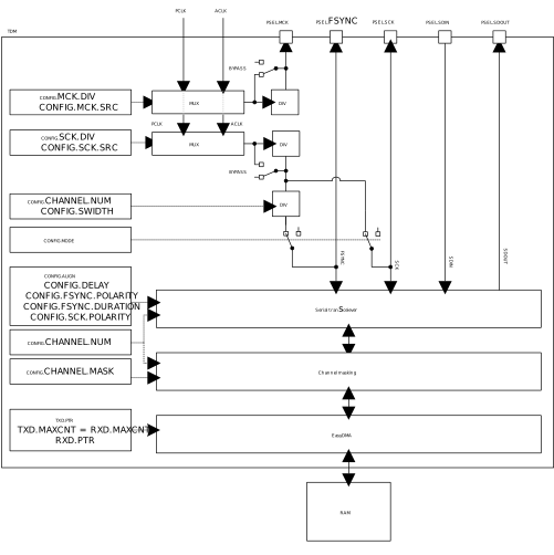
Overview
The TDM interface is comprised of a frame synchronization pulse (FSYNC), a serial clock (SCLK), and the serial audio data (SDIN or SDOUT).
The Master always supplies the clock signals FSYNC and SCK to the Slave. Serial data can be received on the input data pin SDIN, or transmitted on the output data pin SDOUT.
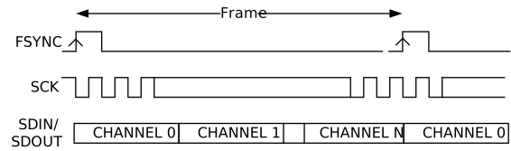
Transmitting and receiving
TDM supports both transmission (TX) and reception (RX) of serial data. In both cases the serial data is shifted synchronously to the SCK clock signal.
TX data is written to the SDOUT pin on the falling edge of SCK, and RX data is read from the SDIN pin on the rising edge of SCK. To change the active edge of SCK, use register CONFIG.SCK.POLARITY.
The most significant bit (MSB) is always transmitted first.
TX and RX are available in both Master and Slave modes and can be enabled/disabled independently in CONFIG.RXTXEN.
Transmission and/or reception is started by triggering the START task. When transmission is enabled in CONFIG.TXEN), the TXPTRUPD event will be generated for every number of transmitted data words given by TXD.MAXCNT. Each data word contains one or more samples. The TXPTRUPD event is generated just before MAXCNT number of bytes have been transmitted. Similarly, when reception is enabled in CONFIG.RXTXEN, the RXPTRUPD event is generated just after MAXCNT number of bytes have been received.
- When transmitting and receiving, if the receive size (RXD.MAXCNT) exceeds the transmit size (TXD.MAXCNT), additional bytes are sent after TXD.MAXCNT bytes have been transmitted. These extra bytes are being sent while RXD.MAXCNT bytes are received and continue until the frame is completed.
- When only transmitting, extra samples are sent after TXD.MAXCNT bytes have been transmitted to complete the frame.
If transmitting more samples than receiving (TXD.MAXCNT is larger than RXD.MAXCNT), the additional received samples will be discarded.
During receive-only operation, once RXD.MAXCNT bytes have been received, any further samples are discarded.
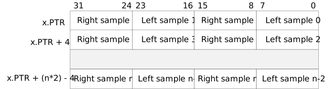
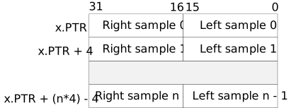
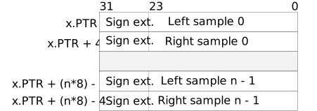
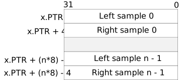
CONFIG.ORS follows the layout of a 32-bit memory word and can contain four 8-bit samples, two 16-bit samples, one right-aligned 24-bit sample sign-extended to 32 bit, or one 32-bit sample. The size of the samples is dependent on CONFIG.SWIDTH. For details on the memory word layout, see Channel mask and EasyDMA.
The MAXCNT event is generated synchronously to the active FSYNC edge at the beginning of a frame after transmitting RXD.MAXCNT bytes. The initial MAXCNT event is generated at the first active edge of FSYNC after the START task has been triggered. The MAXCNT event is generated once all data has been transmitted and/or received. The data will be available in RAM upon completion of the EasyDMA operation.
Transmission can be aborted by using the ABORT task. This will abort TDM transfer possibly without completing MAXCNT words, and will cause the ABORTED event to be generated.
- CONFIG.FSYNC.DURATION = Channel
- CONFIG.FSYNC.CPOLARITY = PosEdge
- CONFIG.SWIDTH = 8Bit
- CONFIG.CHANNEL.NUM = Tdm2Ch
- CONFIG.CHANNEL.DELAY = Delay0Ck
- TXD.MAXCNT = 1
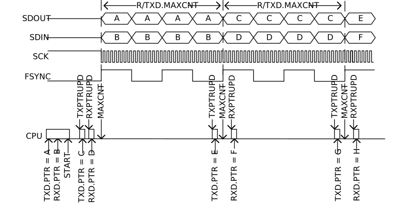
Clocks
In addition to the frame sync (FSYNC) pulse, TDM has two clock signals. The master clock MCK and the sample data bit clock SCK.
MCK and SCK are independent and can be configured individually.
The serial clock (SCK), often referred to as the serial bit clock, pulses once for each data bit being transferred on the serial data lines SDIN and SDOUT.
The polarity of SCK is configured in CONFIG.SCK.POLARITY.
When operating in Master mode, SCK clock source and frequency and is configured in CONFIG.SCK.SRC and CONFIG.SCK.DIV respectively. For CONFIG.SCK.DIV value, see Clock divider equations.
When operating in Slave mode, SCK is an input signal provided by the external master.
The optional master clock (MCK) is independent from SCK and FSYNC.
The master clock generator is enabled/disabled using CONFIG.MCK.EN, and the generator is started or stopped by the START or STOP tasks respectively.
Frame synchronization pulse (FSYNC)
FSYNC defines the start of the frame in the serial bit streams sent and received on SDOUT and SDIN, respectively. It is often referred to as "word clock", "sample clock", "word select", "frame clock", or "left/right clock".
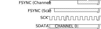
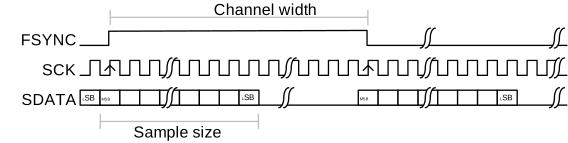
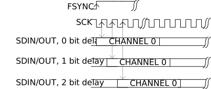
When TDM is configured for the I2S mode, each frame contains one left and right sample pair, with the left sample being transferred during the low half period of FSYNC followed by the right sample being transferred during the high half period of FSYNC. There is a single SCK clock pulse delay between FSYNC edge and the first bit of the sample.
With the Aligned format, each frame contains one left and right sample pair, with the left sample being transferred during the high half period of FSYNC followed by the right sample being transferred during the low half period of FSYNC. There is no delay between FSYNC edge and the first bit of the sample.
For TDM, the active edge of FSYNC defines the beginning of a frame. The words within the frame are transferred continously, with no transitions of FSYNC.
| Format | CONFIG.FSYNC.DURATION | CONFIG.FSYNC.POLARITY | CONFIG.CHANNEL.DELAY |
|---|---|---|---|
| I2S | Channel | Left=NegEdge | Delay1Ck |
| Aligned | Channel | Left=PosEdge | Delay0Ck |
| TDM | Channel or Sck | PosEdge | Delay0Ck, Delay1Ck, or Delay2Ck |
Clock source selection
The clock source for SCK and MCK is selectable in registers CONFIG.MCK.SRC and CONFIG.SCK.SRC respectively.
The following clocks can be selected as the clock source.
- Peripheral clock (PCLK)
- Additional clock (ACLK)
To improve the clock accuracy and jitter performance, it is recommended (but not mandatory) that the PCLK source used is running off the external crystal. The ACLK source requires the use of a crystal. See CLOCK — Clock control for more information about clock sources.
The clock generator can be bypassed so that MCK or SCK is derived directly from the input source. This can be configured in the BYPASS field of their respective registers CONFIG.SCK.SRC and CONFIG.SCK.SRC.
Clock frequency selection
MCK and SCK frequency can be adjusted on-the-fly by using CONFIG.MCK.DIV or CONFIG.SCK.DIV.
Clock divider equations
The following equations are used to select SCK and MCK frequencies.
- fCK is the SCK or MCK frequency in Hz.
- fsource is the frequency of the selected clock source, either ACLK or PCLK.
- DIV is the CONFIG.SCK.DIV or CONFIG.MCK.DIV register value.
The first equation is used to calculate the value of CONFIG.MCK.DIV or CONFIG.SCK.DIV for a given source, and MCK or SCK frequency.
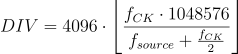
Because of rounding errors, an accurate MCK clock may not be achievable. The equation does not take into account the maximum register values of CONFIG.MCK.DIV or CONFIG.SCK.DIV.
The actual MCK or SCK frequency can be calculated using the equation below.
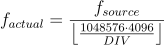
The clock error can be calculated using the equation below. The error e is the percentage difference from the requested fMCK or fSCK frequency.

Width and alignment
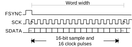
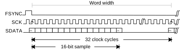
Each audio data sample is followed by sufficient number of zero data bits to complete an M-bit word. The CONFIG.SWIDTH register defines the sample width of the data read and written to memory, as well as the number of SCK clock cycles per word. The M-bit word is sometimes referred to as a channel block.
Alignment of samples
If the word width differs from the sample width, the sample value can be either right or left-aligned inside a word, as specified in CONFIG.ALIGN.


Channel mask and EasyDMA
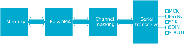
TDM implements EasyDMA for accessing RAM without CPU intervention.
EasyDMA
The source and destination pointers for the TX and RX data are configured in TXD.PTR and RXD.PTR. The memory pointed to by these pointers will only be read or written when TX or RX are enabled in and .
The addresses written to the pointer registers TXD.PTR and RXD.PTR are double-buffered in hardware, and these double buffers are updated for every TXD.MAXCNT/RXD.MAXCNT words (containing one or more samples) read/written from/to memory. The events TXPTRUPD and RXPTRUPD are generated whenever the TXD.PTR and RXD.PTR are transferred to these double buffers.
If TXD.PTR is not pointing to the Data RAM region when transmission is enabled, or RXD.PTR is not pointing to the Data RAM region when reception is enabled, an EasyDMA transfer may result in a HardFault and/or memory corruption. See Memory for more information about the different memory regions.
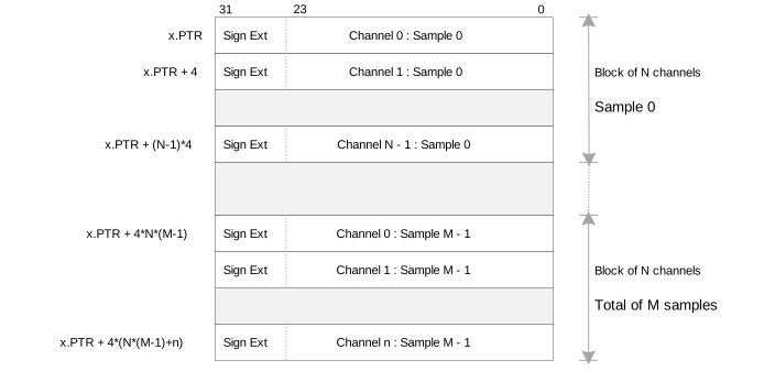
The size of the RXD and TXD memory buffers are independent, but the number of transmitted bytes always equals the number of received bytes. With RXD.MAXCNT and TXD.MAXCNT being independent, data is either discarded or padded as described in Transmitting and receiving. The size of the buffers is specified in a number of bytes, however the memory is organized in 32-bit words that either contain four 8-bit samples, two 16-bit samples, one right-aligned 24-bit sample sign extended to 32 bit, or one 32-bit sample.
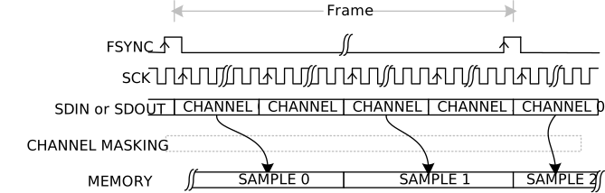
Channel masking
Memory map for single channel (mono)
When the resulting data after channel masking is a single channel, the following figures show how this channel's samples are mapped to memory. The mapping is valid for both RX and TX.
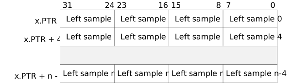
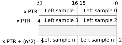
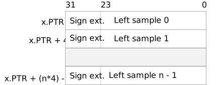
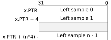
Memory map for two channels (stereo)
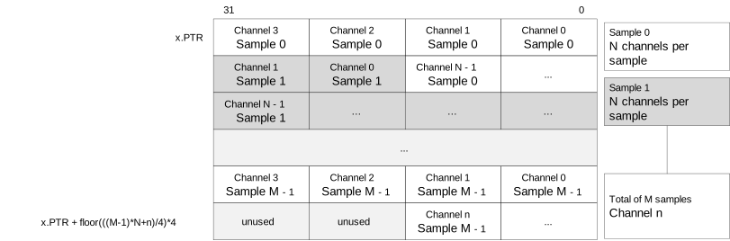
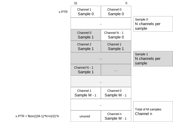
When the resulting data after channel masking is two channels (stereo), the following figures show how this channel's samples are mapped to memory. The mapping is valid for both RX and TX.
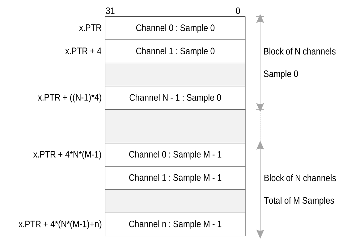
Memory map for multi-channel (three or more)
- S is the number of data bits in a sample
- N total number of channels per sample
- n is the channel number of the current sample
- m is the sample number
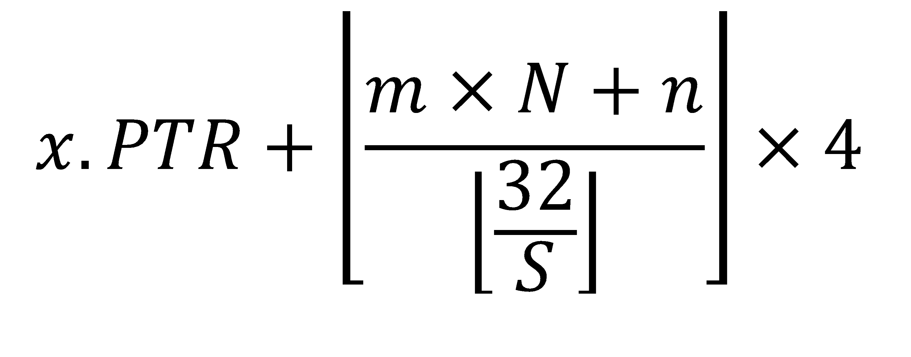
When the resulting data after channel masking is three or more the samples are stored sequentially in memory, similar to stereo. The following figures show how the samples are mapped to memory. The mapping is valid for both RX and TX.
Pin configuration
The MCK, SCK, FSYNC, SDIN and SDOUT signals associated with TDM are mapped to physical pins according to the pin numbers specified in the PSEL.x registers.
These pins are acquired whenever TDM is enabled through the register ENABLE.
When a pin is acquired by TDM, the direction of the pin (input or output) will be configured automatically, and any pin direction setting done in the GPIO module will be overridden. The directions for the various TDM pins are shown in the following tables.
To secure correct signal levels on the pins in System OFF mode, and when TDM is disabled, these pins must be configured in the GPIO peripheral directly.
| TDM signal | TDM pin | Direction | Output value | Comment |
|---|---|---|---|---|
| MCK | As specified in PSEL.MCK | Output | 0 | |
| FSYNC | As specified in PSEL.FSYNC | Output | 0 | |
| SCK | As specified in PSEL.SCK | Output | 0 | |
| SDIN | As specified in PSEL.SDIN | Input | Not applicable | |
| SDOUT | As specified in PSEL.SDOUT | Output | 0 |
| TDM signal | TDM pin | Direction | Output value | Comment |
|---|---|---|---|---|
| MCK | As specified in PSEL.MCK | Output | 0 | |
| FSYNC | As specified in PSEL.FSYNC | Input | Not applicable | |
| SCK | As specified in PSEL.SCK | Input | Not applicable | |
| SDIN | As specified in PSEL.SDIN | Input | Not applicable | |
| SDOUT | As specified in PSEL.SDOUT | Output | 0 |
Registers
Instances
| Instance | Domain | Base address | TrustZone | Split access | Description | ||
|---|---|---|---|---|---|---|---|
| Map | Att | DMA | |||||
TDM : S | GLOBAL | 0x500E8000 | US | S | SA | No | Time division multiplexed audio interface TDM |
Configuration
| Instance | Domain | Configuration |
|---|---|---|
TDM : S | GLOBAL | Use GPIO port P1 or P3 ACLK is the fixed 24 MHz clock PCLK24M PCLK is the fixed 32 MHz clock PCLK32M CURRENTAMOUNT register included. |
Register overview
| Register | Offset | TZ | Description |
|---|---|---|---|
| TASKS_START | 0x000 | Starts continuous TDM transfer. Also starts MCK when this is enabled | |
| TASKS_STOP | 0x004 | Stops TDM transfer after the completion of MAXCNT bytes. Triggering this task will cause the STOPPED event to be generated. | |
| TASKS_ABORT | 0x008 | Abort TDM transfer without completing MAXCNT bytes. Triggering this task will cause the ABORTED event to be generated. | |
| SUBSCRIBE_START | 0x080 | Subscribe configuration for task START | |
| SUBSCRIBE_STOP | 0x084 | Subscribe configuration for task STOP | |
| SUBSCRIBE_ABORT | 0x088 | Subscribe configuration for task ABORT | |
| EVENTS_RXPTRUPD | 0x104 | The RXD.PTR register has been copied to internal double-buffers. When TDM is started and RX is enabled, this event will be generated for every RXTXD.MAXCNT bytes received on the SDIN pin. | |
| EVENTS_STOPPED | 0x108 | Transfer stopped. | |
| EVENTS_ABORTED | 0x10C | Transfer aborted. | |
| EVENTS_TXPTRUPD | 0x118 | The TDX.PTR register has been copied to internal double-buffers. When TDM is started and TX is enabled, this event will be generated for every RXTXD.MAXCNT bytes that are sent on the SDOUT pin. | |
| EVENTS_MAXCNT | 0x120 | Generated on the active edge of FSYNC, after both RX and TX DMA transfers have completed. An initial MAXCNT event is also triggered on the first active edge of FSYNC after the START task is issued. | |
| EVENTS_BUSERROR_RX | 0x124 | This event is generated if an error occurs during the bus transfer. | |
| EVENTS_BUSERROR_TX | 0x128 | This event is generated if an error occurs during the bus transfer. | |
| PUBLISH_RXPTRUPD | 0x184 | Publish configuration for event RXPTRUPD | |
| PUBLISH_STOPPED | 0x188 | Publish configuration for event STOPPED | |
| PUBLISH_ABORTED | 0x18C | Publish configuration for event ABORTED | |
| PUBLISH_TXPTRUPD | 0x198 | Publish configuration for event TXPTRUPD | |
| PUBLISH_MAXCNT | 0x1A0 | Publish configuration for event MAXCNT | |
| PUBLISH_BUSERROR_RX | 0x1A4 | Publish configuration for event BUSERROR_RX | |
| PUBLISH_BUSERROR_TX | 0x1A8 | Publish configuration for event BUSERROR_TX | |
| INTEN | 0x300 | Enable or disable interrupt | |
| INTENSET | 0x304 | Enable interrupt | |
| INTENCLR | 0x308 | Disable interrupt | |
| INTPEND | 0x30C | Pending interrupts | |
| ENABLE | 0x500 | Enable TDM | |
| CONFIG.MODE | 0x504 | Mode configuration | |
| CONFIG.RXTXEN | 0x508 | Reception (RX) and transmission (TX) enable. | |
| CONFIG.MCK.EN | 0x50C | Master clock generator enable. | |
| CONFIG.MCK.DIV | 0x510 | MCK divider. | |
| CONFIG.MCK.SRC | 0x514 | MCK clock source selection | |
| CONFIG.SCK.DIV | 0x518 | SCK divider. | |
| CONFIG.SCK.SRC | 0x51C | SCK clock source selection | |
| CONFIG.SCK.POLARITY | 0x520 | Set SCK Polarity. | |
| CONFIG.SWIDTH | 0x524 | Sample and word width configuration. | |
| CONFIG.ALIGN | 0x528 | Alignment of sample within the audio data word. | |
| CONFIG.CHANNEL.MASK | 0x52C | Select which channels are to be used. | |
| CONFIG.CHANNEL.NUM | 0x530 | Select number of channels. | |
| CONFIG.CHANNEL.DELAY | 0x534 | Set channel delay. | |
| CONFIG.FSYNC.POLARITY | 0x538 | Set FSYNC Polarity. | |
| CONFIG.FSYNC.DURATION | 0x53C | Set FSYNC duration. | |
| CONFIG.ORS | 0x540 | Over-read sample: Extra sample(s) to be transmitted after TXD.MAXCNT bytes have been transmitted. | |
| PSEL.MCK | 0x570 | Pin select for MCK signal | |
| PSEL.SCK | 0x574 | Pin select for SCK signal | |
| PSEL.FSYNC | 0x578 | Pin select for FSYNC signal | |
| PSEL.SDIN | 0x57C | Pin select for SDIN signal | |
| PSEL.SDOUT | 0x580 | Pin select for SDOUT signal | |
| RXD.PTR | 0x704 | RAM buffer start address | |
| RXD.MAXCNT | 0x708 | Maximum number of bytes in channel buffer | |
| RXD.AMOUNT | 0x70C | Number of bytes transferred in the last transaction, updated after the END event. | |
| RXD.CURRENTAMOUNT | 0x710 | Number of bytes transferred in the current transaction | |
| RXD.MODE | 0x718 | Configure EasyDMA mode | |
| RXD.TERMINATEONBUSERROR | 0x71C | Terminate the transaction if a BUSERROR event is detected. | |
| RXD.BUSERRORADDRESS | 0x720 | Address of transaction that generated the last BUSERROR event. | |
| TXD.PTR | 0x744 | RAM buffer start address | |
| TXD.MAXCNT | 0x748 | Maximum number of bytes in channel buffer | |
| TXD.AMOUNT | 0x74C | Number of bytes transferred in the last transaction, updated after the END event. | |
| TXD.CURRENTAMOUNT | 0x750 | Number of bytes transferred in the current transaction | |
| TXD.MODE | 0x758 | Configure EasyDMA mode | |
| TXD.TERMINATEONBUSERROR | 0x75C | Terminate the transaction if a BUSERROR event is detected. | |
| TXD.BUSERRORADDRESS | 0x760 | Address of transaction that generated the last BUSERROR event. |
TASKS_START
Address offset: 0x000
Starts continuous TDM transfer. Also starts MCK when this is enabled
| Bit number | 31 | 30 | 29 | 28 | 27 | 26 | 25 | 24 | 23 | 22 | 21 | 20 | 19 | 18 | 17 | 16 | 15 | 14 | 13 | 12 | 11 | 10 | 9 | 8 | 7 | 6 | 5 | 4 | 3 | 2 | 1 | 0 | |||
|---|---|---|---|---|---|---|---|---|---|---|---|---|---|---|---|---|---|---|---|---|---|---|---|---|---|---|---|---|---|---|---|---|---|---|---|
| ID | A | ||||||||||||||||||||||||||||||||||
| Reset 0x00000000 | 0 | 0 | 0 | 0 | 0 | 0 | 0 | 0 | 0 | 0 | 0 | 0 | 0 | 0 | 0 | 0 | 0 | 0 | 0 | 0 | 0 | 0 | 0 | 0 | 0 | 0 | 0 | 0 | 0 | 0 | 0 | 0 | |||
| ID | R/W | Field | Value ID | Value | Description | ||||||||||||||||||||||||||||||
| A | W | TASKS_START | Starts continuous TDM transfer. Also starts MCK when this is enabled | ||||||||||||||||||||||||||||||||
Trigger | 1 | Trigger task | |||||||||||||||||||||||||||||||||
TASKS_STOP
Address offset: 0x004
Stops TDM transfer after the completion of MAXCNT bytes. Triggering this task will cause the STOPPED event to be generated.
| Bit number | 31 | 30 | 29 | 28 | 27 | 26 | 25 | 24 | 23 | 22 | 21 | 20 | 19 | 18 | 17 | 16 | 15 | 14 | 13 | 12 | 11 | 10 | 9 | 8 | 7 | 6 | 5 | 4 | 3 | 2 | 1 | 0 | |||
|---|---|---|---|---|---|---|---|---|---|---|---|---|---|---|---|---|---|---|---|---|---|---|---|---|---|---|---|---|---|---|---|---|---|---|---|
| ID | A | ||||||||||||||||||||||||||||||||||
| Reset 0x00000000 | 0 | 0 | 0 | 0 | 0 | 0 | 0 | 0 | 0 | 0 | 0 | 0 | 0 | 0 | 0 | 0 | 0 | 0 | 0 | 0 | 0 | 0 | 0 | 0 | 0 | 0 | 0 | 0 | 0 | 0 | 0 | 0 | |||
| ID | R/W | Field | Value ID | Value | Description | ||||||||||||||||||||||||||||||
| A | W | TASKS_STOP | Stops TDM transfer after the completion of MAXCNT bytes. Triggering this task will cause the STOPPED event to be generated. | ||||||||||||||||||||||||||||||||
Trigger | 1 | Trigger task | |||||||||||||||||||||||||||||||||
TASKS_ABORT
Address offset: 0x008
Abort TDM transfer without completing MAXCNT bytes. Triggering this task will cause the ABORTED event to be generated.
| Bit number | 31 | 30 | 29 | 28 | 27 | 26 | 25 | 24 | 23 | 22 | 21 | 20 | 19 | 18 | 17 | 16 | 15 | 14 | 13 | 12 | 11 | 10 | 9 | 8 | 7 | 6 | 5 | 4 | 3 | 2 | 1 | 0 | |||
|---|---|---|---|---|---|---|---|---|---|---|---|---|---|---|---|---|---|---|---|---|---|---|---|---|---|---|---|---|---|---|---|---|---|---|---|
| ID | A | ||||||||||||||||||||||||||||||||||
| Reset 0x00000000 | 0 | 0 | 0 | 0 | 0 | 0 | 0 | 0 | 0 | 0 | 0 | 0 | 0 | 0 | 0 | 0 | 0 | 0 | 0 | 0 | 0 | 0 | 0 | 0 | 0 | 0 | 0 | 0 | 0 | 0 | 0 | 0 | |||
| ID | R/W | Field | Value ID | Value | Description | ||||||||||||||||||||||||||||||
| A | W | TASKS_ABORT | Abort TDM transfer without completing MAXCNT bytes. Triggering this task will cause the ABORTED event to be generated. | ||||||||||||||||||||||||||||||||
Trigger | 1 | Trigger task | |||||||||||||||||||||||||||||||||
SUBSCRIBE_START
Address offset: 0x080
Subscribe configuration for task START
| Bit number | 31 | 30 | 29 | 28 | 27 | 26 | 25 | 24 | 23 | 22 | 21 | 20 | 19 | 18 | 17 | 16 | 15 | 14 | 13 | 12 | 11 | 10 | 9 | 8 | 7 | 6 | 5 | 4 | 3 | 2 | 1 | 0 | |||
|---|---|---|---|---|---|---|---|---|---|---|---|---|---|---|---|---|---|---|---|---|---|---|---|---|---|---|---|---|---|---|---|---|---|---|---|
| ID | B | A | A | A | A | A | A | A | A | ||||||||||||||||||||||||||
| Reset 0x00000000 | 0 | 0 | 0 | 0 | 0 | 0 | 0 | 0 | 0 | 0 | 0 | 0 | 0 | 0 | 0 | 0 | 0 | 0 | 0 | 0 | 0 | 0 | 0 | 0 | 0 | 0 | 0 | 0 | 0 | 0 | 0 | 0 | |||
| ID | R/W | Field | Value ID | Value | Description | ||||||||||||||||||||||||||||||
| A | RW | CHIDX | [0..255] | DPPI channel that task START will subscribe to | |||||||||||||||||||||||||||||||
| B | RW | EN | |||||||||||||||||||||||||||||||||
Disabled | 0 | Disable subscription | |||||||||||||||||||||||||||||||||
Enabled | 1 | Enable subscription | |||||||||||||||||||||||||||||||||
SUBSCRIBE_STOP
Address offset: 0x084
Subscribe configuration for task STOP
| Bit number | 31 | 30 | 29 | 28 | 27 | 26 | 25 | 24 | 23 | 22 | 21 | 20 | 19 | 18 | 17 | 16 | 15 | 14 | 13 | 12 | 11 | 10 | 9 | 8 | 7 | 6 | 5 | 4 | 3 | 2 | 1 | 0 | |||
|---|---|---|---|---|---|---|---|---|---|---|---|---|---|---|---|---|---|---|---|---|---|---|---|---|---|---|---|---|---|---|---|---|---|---|---|
| ID | B | A | A | A | A | A | A | A | A | ||||||||||||||||||||||||||
| Reset 0x00000000 | 0 | 0 | 0 | 0 | 0 | 0 | 0 | 0 | 0 | 0 | 0 | 0 | 0 | 0 | 0 | 0 | 0 | 0 | 0 | 0 | 0 | 0 | 0 | 0 | 0 | 0 | 0 | 0 | 0 | 0 | 0 | 0 | |||
| ID | R/W | Field | Value ID | Value | Description | ||||||||||||||||||||||||||||||
| A | RW | CHIDX | [0..255] | DPPI channel that task STOP will subscribe to | |||||||||||||||||||||||||||||||
| B | RW | EN | |||||||||||||||||||||||||||||||||
Disabled | 0 | Disable subscription | |||||||||||||||||||||||||||||||||
Enabled | 1 | Enable subscription | |||||||||||||||||||||||||||||||||
SUBSCRIBE_ABORT
Address offset: 0x088
Subscribe configuration for task ABORT
| Bit number | 31 | 30 | 29 | 28 | 27 | 26 | 25 | 24 | 23 | 22 | 21 | 20 | 19 | 18 | 17 | 16 | 15 | 14 | 13 | 12 | 11 | 10 | 9 | 8 | 7 | 6 | 5 | 4 | 3 | 2 | 1 | 0 | |||
|---|---|---|---|---|---|---|---|---|---|---|---|---|---|---|---|---|---|---|---|---|---|---|---|---|---|---|---|---|---|---|---|---|---|---|---|
| ID | B | A | A | A | A | A | A | A | A | ||||||||||||||||||||||||||
| Reset 0x00000000 | 0 | 0 | 0 | 0 | 0 | 0 | 0 | 0 | 0 | 0 | 0 | 0 | 0 | 0 | 0 | 0 | 0 | 0 | 0 | 0 | 0 | 0 | 0 | 0 | 0 | 0 | 0 | 0 | 0 | 0 | 0 | 0 | |||
| ID | R/W | Field | Value ID | Value | Description | ||||||||||||||||||||||||||||||
| A | RW | CHIDX | [0..255] | DPPI channel that task ABORT will subscribe to | |||||||||||||||||||||||||||||||
| B | RW | EN | |||||||||||||||||||||||||||||||||
Disabled | 0 | Disable subscription | |||||||||||||||||||||||||||||||||
Enabled | 1 | Enable subscription | |||||||||||||||||||||||||||||||||
EVENTS_RXPTRUPD
Address offset: 0x104
The RXD.PTR register has been copied to internal double-buffers. When TDM is started and RX is enabled, this event will be generated for every RXTXD.MAXCNT bytes received on the SDIN pin.
| Bit number | 31 | 30 | 29 | 28 | 27 | 26 | 25 | 24 | 23 | 22 | 21 | 20 | 19 | 18 | 17 | 16 | 15 | 14 | 13 | 12 | 11 | 10 | 9 | 8 | 7 | 6 | 5 | 4 | 3 | 2 | 1 | 0 | |||
|---|---|---|---|---|---|---|---|---|---|---|---|---|---|---|---|---|---|---|---|---|---|---|---|---|---|---|---|---|---|---|---|---|---|---|---|
| ID | A | ||||||||||||||||||||||||||||||||||
| Reset 0x00000000 | 0 | 0 | 0 | 0 | 0 | 0 | 0 | 0 | 0 | 0 | 0 | 0 | 0 | 0 | 0 | 0 | 0 | 0 | 0 | 0 | 0 | 0 | 0 | 0 | 0 | 0 | 0 | 0 | 0 | 0 | 0 | 0 | |||
| ID | R/W | Field | Value ID | Value | Description | ||||||||||||||||||||||||||||||
| A | RW | EVENTS_RXPTRUPD | The RXD.PTR register has been copied to internal double-buffers. When TDM is started and RX is enabled, this event will be generated for every RXTXD.MAXCNT bytes received on the SDIN pin. | ||||||||||||||||||||||||||||||||
NotGenerated | 0 | Event not generated | |||||||||||||||||||||||||||||||||
Generated | 1 | Event generated | |||||||||||||||||||||||||||||||||
EVENTS_STOPPED
Address offset: 0x108
Transfer stopped.
| Bit number | 31 | 30 | 29 | 28 | 27 | 26 | 25 | 24 | 23 | 22 | 21 | 20 | 19 | 18 | 17 | 16 | 15 | 14 | 13 | 12 | 11 | 10 | 9 | 8 | 7 | 6 | 5 | 4 | 3 | 2 | 1 | 0 | |||
|---|---|---|---|---|---|---|---|---|---|---|---|---|---|---|---|---|---|---|---|---|---|---|---|---|---|---|---|---|---|---|---|---|---|---|---|
| ID | A | ||||||||||||||||||||||||||||||||||
| Reset 0x00000000 | 0 | 0 | 0 | 0 | 0 | 0 | 0 | 0 | 0 | 0 | 0 | 0 | 0 | 0 | 0 | 0 | 0 | 0 | 0 | 0 | 0 | 0 | 0 | 0 | 0 | 0 | 0 | 0 | 0 | 0 | 0 | 0 | |||
| ID | R/W | Field | Value ID | Value | Description | ||||||||||||||||||||||||||||||
| A | RW | EVENTS_STOPPED | Transfer stopped. | ||||||||||||||||||||||||||||||||
NotGenerated | 0 | Event not generated | |||||||||||||||||||||||||||||||||
Generated | 1 | Event generated | |||||||||||||||||||||||||||||||||
EVENTS_ABORTED
Address offset: 0x10C
Transfer aborted.
| Bit number | 31 | 30 | 29 | 28 | 27 | 26 | 25 | 24 | 23 | 22 | 21 | 20 | 19 | 18 | 17 | 16 | 15 | 14 | 13 | 12 | 11 | 10 | 9 | 8 | 7 | 6 | 5 | 4 | 3 | 2 | 1 | 0 | |||
|---|---|---|---|---|---|---|---|---|---|---|---|---|---|---|---|---|---|---|---|---|---|---|---|---|---|---|---|---|---|---|---|---|---|---|---|
| ID | A | ||||||||||||||||||||||||||||||||||
| Reset 0x00000000 | 0 | 0 | 0 | 0 | 0 | 0 | 0 | 0 | 0 | 0 | 0 | 0 | 0 | 0 | 0 | 0 | 0 | 0 | 0 | 0 | 0 | 0 | 0 | 0 | 0 | 0 | 0 | 0 | 0 | 0 | 0 | 0 | |||
| ID | R/W | Field | Value ID | Value | Description | ||||||||||||||||||||||||||||||
| A | RW | EVENTS_ABORTED | Transfer aborted. | ||||||||||||||||||||||||||||||||
NotGenerated | 0 | Event not generated | |||||||||||||||||||||||||||||||||
Generated | 1 | Event generated | |||||||||||||||||||||||||||||||||
EVENTS_TXPTRUPD
Address offset: 0x118
The TDX.PTR register has been copied to internal double-buffers. When TDM is started and TX is enabled, this event will be generated for every RXTXD.MAXCNT bytes that are sent on the SDOUT pin.
| Bit number | 31 | 30 | 29 | 28 | 27 | 26 | 25 | 24 | 23 | 22 | 21 | 20 | 19 | 18 | 17 | 16 | 15 | 14 | 13 | 12 | 11 | 10 | 9 | 8 | 7 | 6 | 5 | 4 | 3 | 2 | 1 | 0 | |||
|---|---|---|---|---|---|---|---|---|---|---|---|---|---|---|---|---|---|---|---|---|---|---|---|---|---|---|---|---|---|---|---|---|---|---|---|
| ID | A | ||||||||||||||||||||||||||||||||||
| Reset 0x00000000 | 0 | 0 | 0 | 0 | 0 | 0 | 0 | 0 | 0 | 0 | 0 | 0 | 0 | 0 | 0 | 0 | 0 | 0 | 0 | 0 | 0 | 0 | 0 | 0 | 0 | 0 | 0 | 0 | 0 | 0 | 0 | 0 | |||
| ID | R/W | Field | Value ID | Value | Description | ||||||||||||||||||||||||||||||
| A | RW | EVENTS_TXPTRUPD | The TDX.PTR register has been copied to internal double-buffers. When TDM is started and TX is enabled, this event will be generated for every RXTXD.MAXCNT bytes that are sent on the SDOUT pin. | ||||||||||||||||||||||||||||||||
NotGenerated | 0 | Event not generated | |||||||||||||||||||||||||||||||||
Generated | 1 | Event generated | |||||||||||||||||||||||||||||||||
EVENTS_MAXCNT
Address offset: 0x120
Generated on the active edge of FSYNC, after both RX and TX DMA transfers have completed. An initial MAXCNT event is also triggered on the first active edge of FSYNC after the START task is issued.
| Bit number | 31 | 30 | 29 | 28 | 27 | 26 | 25 | 24 | 23 | 22 | 21 | 20 | 19 | 18 | 17 | 16 | 15 | 14 | 13 | 12 | 11 | 10 | 9 | 8 | 7 | 6 | 5 | 4 | 3 | 2 | 1 | 0 | |||
|---|---|---|---|---|---|---|---|---|---|---|---|---|---|---|---|---|---|---|---|---|---|---|---|---|---|---|---|---|---|---|---|---|---|---|---|
| ID | A | ||||||||||||||||||||||||||||||||||
| Reset 0x00000000 | 0 | 0 | 0 | 0 | 0 | 0 | 0 | 0 | 0 | 0 | 0 | 0 | 0 | 0 | 0 | 0 | 0 | 0 | 0 | 0 | 0 | 0 | 0 | 0 | 0 | 0 | 0 | 0 | 0 | 0 | 0 | 0 | |||
| ID | R/W | Field | Value ID | Value | Description | ||||||||||||||||||||||||||||||
| A | RW | EVENTS_MAXCNT | Generated on the active edge of FSYNC, after both RX and TX DMA transfers have completed. An initial MAXCNT event is also triggered on the first active edge of FSYNC after the START task is issued. | ||||||||||||||||||||||||||||||||
NotGenerated | 0 | Event not generated | |||||||||||||||||||||||||||||||||
Generated | 1 | Event generated | |||||||||||||||||||||||||||||||||
EVENTS_BUSERROR_RX
Address offset: 0x124
This event is generated if an error occurs during the bus transfer.
When this event is generated, the address which caused the error can be read from the RXD.BUSERRORADDRESS register.
| Bit number | 31 | 30 | 29 | 28 | 27 | 26 | 25 | 24 | 23 | 22 | 21 | 20 | 19 | 18 | 17 | 16 | 15 | 14 | 13 | 12 | 11 | 10 | 9 | 8 | 7 | 6 | 5 | 4 | 3 | 2 | 1 | 0 | |||
|---|---|---|---|---|---|---|---|---|---|---|---|---|---|---|---|---|---|---|---|---|---|---|---|---|---|---|---|---|---|---|---|---|---|---|---|
| ID | A | ||||||||||||||||||||||||||||||||||
| Reset 0x00000000 | 0 | 0 | 0 | 0 | 0 | 0 | 0 | 0 | 0 | 0 | 0 | 0 | 0 | 0 | 0 | 0 | 0 | 0 | 0 | 0 | 0 | 0 | 0 | 0 | 0 | 0 | 0 | 0 | 0 | 0 | 0 | 0 | |||
| ID | R/W | Field | Value ID | Value | Description | ||||||||||||||||||||||||||||||
| A | RW | EVENTS_BUSERROR_RX | This event is generated if an error occurs during the bus transfer. When this event is generated, the address which caused the error can be read from the RXD.BUSERRORADDRESS register. | ||||||||||||||||||||||||||||||||
NotGenerated | 0 | Event not generated | |||||||||||||||||||||||||||||||||
Generated | 1 | Event generated | |||||||||||||||||||||||||||||||||
EVENTS_BUSERROR_TX
Address offset: 0x128
This event is generated if an error occurs during the bus transfer.
When this event is generated, the address which caused the error can be read from the TXD.BUSERRORADDRESS register.
| Bit number | 31 | 30 | 29 | 28 | 27 | 26 | 25 | 24 | 23 | 22 | 21 | 20 | 19 | 18 | 17 | 16 | 15 | 14 | 13 | 12 | 11 | 10 | 9 | 8 | 7 | 6 | 5 | 4 | 3 | 2 | 1 | 0 | |||
|---|---|---|---|---|---|---|---|---|---|---|---|---|---|---|---|---|---|---|---|---|---|---|---|---|---|---|---|---|---|---|---|---|---|---|---|
| ID | A | ||||||||||||||||||||||||||||||||||
| Reset 0x00000000 | 0 | 0 | 0 | 0 | 0 | 0 | 0 | 0 | 0 | 0 | 0 | 0 | 0 | 0 | 0 | 0 | 0 | 0 | 0 | 0 | 0 | 0 | 0 | 0 | 0 | 0 | 0 | 0 | 0 | 0 | 0 | 0 | |||
| ID | R/W | Field | Value ID | Value | Description | ||||||||||||||||||||||||||||||
| A | RW | EVENTS_BUSERROR_TX | This event is generated if an error occurs during the bus transfer. When this event is generated, the address which caused the error can be read from the TXD.BUSERRORADDRESS register. | ||||||||||||||||||||||||||||||||
NotGenerated | 0 | Event not generated | |||||||||||||||||||||||||||||||||
Generated | 1 | Event generated | |||||||||||||||||||||||||||||||||
PUBLISH_RXPTRUPD
Address offset: 0x184
Publish configuration for event RXPTRUPD
| Bit number | 31 | 30 | 29 | 28 | 27 | 26 | 25 | 24 | 23 | 22 | 21 | 20 | 19 | 18 | 17 | 16 | 15 | 14 | 13 | 12 | 11 | 10 | 9 | 8 | 7 | 6 | 5 | 4 | 3 | 2 | 1 | 0 | |||
|---|---|---|---|---|---|---|---|---|---|---|---|---|---|---|---|---|---|---|---|---|---|---|---|---|---|---|---|---|---|---|---|---|---|---|---|
| ID | B | A | A | A | A | A | A | A | A | ||||||||||||||||||||||||||
| Reset 0x00000000 | 0 | 0 | 0 | 0 | 0 | 0 | 0 | 0 | 0 | 0 | 0 | 0 | 0 | 0 | 0 | 0 | 0 | 0 | 0 | 0 | 0 | 0 | 0 | 0 | 0 | 0 | 0 | 0 | 0 | 0 | 0 | 0 | |||
| ID | R/W | Field | Value ID | Value | Description | ||||||||||||||||||||||||||||||
| A | RW | CHIDX | [0..255] | DPPI channel that event RXPTRUPD will publish to | |||||||||||||||||||||||||||||||
| B | RW | EN | |||||||||||||||||||||||||||||||||
Disabled | 0 | Disable publishing | |||||||||||||||||||||||||||||||||
Enabled | 1 | Enable publishing | |||||||||||||||||||||||||||||||||
PUBLISH_STOPPED
Address offset: 0x188
Publish configuration for event STOPPED
| Bit number | 31 | 30 | 29 | 28 | 27 | 26 | 25 | 24 | 23 | 22 | 21 | 20 | 19 | 18 | 17 | 16 | 15 | 14 | 13 | 12 | 11 | 10 | 9 | 8 | 7 | 6 | 5 | 4 | 3 | 2 | 1 | 0 | |||
|---|---|---|---|---|---|---|---|---|---|---|---|---|---|---|---|---|---|---|---|---|---|---|---|---|---|---|---|---|---|---|---|---|---|---|---|
| ID | B | A | A | A | A | A | A | A | A | ||||||||||||||||||||||||||
| Reset 0x00000000 | 0 | 0 | 0 | 0 | 0 | 0 | 0 | 0 | 0 | 0 | 0 | 0 | 0 | 0 | 0 | 0 | 0 | 0 | 0 | 0 | 0 | 0 | 0 | 0 | 0 | 0 | 0 | 0 | 0 | 0 | 0 | 0 | |||
| ID | R/W | Field | Value ID | Value | Description | ||||||||||||||||||||||||||||||
| A | RW | CHIDX | [0..255] | DPPI channel that event STOPPED will publish to | |||||||||||||||||||||||||||||||
| B | RW | EN | |||||||||||||||||||||||||||||||||
Disabled | 0 | Disable publishing | |||||||||||||||||||||||||||||||||
Enabled | 1 | Enable publishing | |||||||||||||||||||||||||||||||||
PUBLISH_ABORTED
Address offset: 0x18C
Publish configuration for event ABORTED
| Bit number | 31 | 30 | 29 | 28 | 27 | 26 | 25 | 24 | 23 | 22 | 21 | 20 | 19 | 18 | 17 | 16 | 15 | 14 | 13 | 12 | 11 | 10 | 9 | 8 | 7 | 6 | 5 | 4 | 3 | 2 | 1 | 0 | |||
|---|---|---|---|---|---|---|---|---|---|---|---|---|---|---|---|---|---|---|---|---|---|---|---|---|---|---|---|---|---|---|---|---|---|---|---|
| ID | B | A | A | A | A | A | A | A | A | ||||||||||||||||||||||||||
| Reset 0x00000000 | 0 | 0 | 0 | 0 | 0 | 0 | 0 | 0 | 0 | 0 | 0 | 0 | 0 | 0 | 0 | 0 | 0 | 0 | 0 | 0 | 0 | 0 | 0 | 0 | 0 | 0 | 0 | 0 | 0 | 0 | 0 | 0 | |||
| ID | R/W | Field | Value ID | Value | Description | ||||||||||||||||||||||||||||||
| A | RW | CHIDX | [0..255] | DPPI channel that event ABORTED will publish to | |||||||||||||||||||||||||||||||
| B | RW | EN | |||||||||||||||||||||||||||||||||
Disabled | 0 | Disable publishing | |||||||||||||||||||||||||||||||||
Enabled | 1 | Enable publishing | |||||||||||||||||||||||||||||||||
PUBLISH_TXPTRUPD
Address offset: 0x198
Publish configuration for event TXPTRUPD
| Bit number | 31 | 30 | 29 | 28 | 27 | 26 | 25 | 24 | 23 | 22 | 21 | 20 | 19 | 18 | 17 | 16 | 15 | 14 | 13 | 12 | 11 | 10 | 9 | 8 | 7 | 6 | 5 | 4 | 3 | 2 | 1 | 0 | |||
|---|---|---|---|---|---|---|---|---|---|---|---|---|---|---|---|---|---|---|---|---|---|---|---|---|---|---|---|---|---|---|---|---|---|---|---|
| ID | B | A | A | A | A | A | A | A | A | ||||||||||||||||||||||||||
| Reset 0x00000000 | 0 | 0 | 0 | 0 | 0 | 0 | 0 | 0 | 0 | 0 | 0 | 0 | 0 | 0 | 0 | 0 | 0 | 0 | 0 | 0 | 0 | 0 | 0 | 0 | 0 | 0 | 0 | 0 | 0 | 0 | 0 | 0 | |||
| ID | R/W | Field | Value ID | Value | Description | ||||||||||||||||||||||||||||||
| A | RW | CHIDX | [0..255] | DPPI channel that event TXPTRUPD will publish to | |||||||||||||||||||||||||||||||
| B | RW | EN | |||||||||||||||||||||||||||||||||
Disabled | 0 | Disable publishing | |||||||||||||||||||||||||||||||||
Enabled | 1 | Enable publishing | |||||||||||||||||||||||||||||||||
PUBLISH_MAXCNT
Address offset: 0x1A0
Publish configuration for event MAXCNT
| Bit number | 31 | 30 | 29 | 28 | 27 | 26 | 25 | 24 | 23 | 22 | 21 | 20 | 19 | 18 | 17 | 16 | 15 | 14 | 13 | 12 | 11 | 10 | 9 | 8 | 7 | 6 | 5 | 4 | 3 | 2 | 1 | 0 | |||
|---|---|---|---|---|---|---|---|---|---|---|---|---|---|---|---|---|---|---|---|---|---|---|---|---|---|---|---|---|---|---|---|---|---|---|---|
| ID | B | A | A | A | A | A | A | A | A | ||||||||||||||||||||||||||
| Reset 0x00000000 | 0 | 0 | 0 | 0 | 0 | 0 | 0 | 0 | 0 | 0 | 0 | 0 | 0 | 0 | 0 | 0 | 0 | 0 | 0 | 0 | 0 | 0 | 0 | 0 | 0 | 0 | 0 | 0 | 0 | 0 | 0 | 0 | |||
| ID | R/W | Field | Value ID | Value | Description | ||||||||||||||||||||||||||||||
| A | RW | CHIDX | [0..255] | DPPI channel that event MAXCNT will publish to | |||||||||||||||||||||||||||||||
| B | RW | EN | |||||||||||||||||||||||||||||||||
Disabled | 0 | Disable publishing | |||||||||||||||||||||||||||||||||
Enabled | 1 | Enable publishing | |||||||||||||||||||||||||||||||||
PUBLISH_BUSERROR_RX
Address offset: 0x1A4
Publish configuration for event BUSERROR_RX
When this event is generated, the address which caused the error can be read from the RXD.BUSERRORADDRESS register.
| Bit number | 31 | 30 | 29 | 28 | 27 | 26 | 25 | 24 | 23 | 22 | 21 | 20 | 19 | 18 | 17 | 16 | 15 | 14 | 13 | 12 | 11 | 10 | 9 | 8 | 7 | 6 | 5 | 4 | 3 | 2 | 1 | 0 | |||
|---|---|---|---|---|---|---|---|---|---|---|---|---|---|---|---|---|---|---|---|---|---|---|---|---|---|---|---|---|---|---|---|---|---|---|---|
| ID | B | A | A | A | A | A | A | A | A | ||||||||||||||||||||||||||
| Reset 0x00000000 | 0 | 0 | 0 | 0 | 0 | 0 | 0 | 0 | 0 | 0 | 0 | 0 | 0 | 0 | 0 | 0 | 0 | 0 | 0 | 0 | 0 | 0 | 0 | 0 | 0 | 0 | 0 | 0 | 0 | 0 | 0 | 0 | |||
| ID | R/W | Field | Value ID | Value | Description | ||||||||||||||||||||||||||||||
| A | RW | CHIDX | [0..255] | DPPI channel that event BUSERROR_RX will publish to | |||||||||||||||||||||||||||||||
| B | RW | EN | |||||||||||||||||||||||||||||||||
Disabled | 0 | Disable publishing | |||||||||||||||||||||||||||||||||
Enabled | 1 | Enable publishing | |||||||||||||||||||||||||||||||||
PUBLISH_BUSERROR_TX
Address offset: 0x1A8
Publish configuration for event BUSERROR_TX
When this event is generated, the address which caused the error can be read from the TXD.BUSERRORADDRESS register.
| Bit number | 31 | 30 | 29 | 28 | 27 | 26 | 25 | 24 | 23 | 22 | 21 | 20 | 19 | 18 | 17 | 16 | 15 | 14 | 13 | 12 | 11 | 10 | 9 | 8 | 7 | 6 | 5 | 4 | 3 | 2 | 1 | 0 | |||
|---|---|---|---|---|---|---|---|---|---|---|---|---|---|---|---|---|---|---|---|---|---|---|---|---|---|---|---|---|---|---|---|---|---|---|---|
| ID | B | A | A | A | A | A | A | A | A | ||||||||||||||||||||||||||
| Reset 0x00000000 | 0 | 0 | 0 | 0 | 0 | 0 | 0 | 0 | 0 | 0 | 0 | 0 | 0 | 0 | 0 | 0 | 0 | 0 | 0 | 0 | 0 | 0 | 0 | 0 | 0 | 0 | 0 | 0 | 0 | 0 | 0 | 0 | |||
| ID | R/W | Field | Value ID | Value | Description | ||||||||||||||||||||||||||||||
| A | RW | CHIDX | [0..255] | DPPI channel that event BUSERROR_TX will publish to | |||||||||||||||||||||||||||||||
| B | RW | EN | |||||||||||||||||||||||||||||||||
Disabled | 0 | Disable publishing | |||||||||||||||||||||||||||||||||
Enabled | 1 | Enable publishing | |||||||||||||||||||||||||||||||||
INTEN
Address offset: 0x300
Enable or disable interrupt
| Bit number | 31 | 30 | 29 | 28 | 27 | 26 | 25 | 24 | 23 | 22 | 21 | 20 | 19 | 18 | 17 | 16 | 15 | 14 | 13 | 12 | 11 | 10 | 9 | 8 | 7 | 6 | 5 | 4 | 3 | 2 | 1 | 0 | |||
|---|---|---|---|---|---|---|---|---|---|---|---|---|---|---|---|---|---|---|---|---|---|---|---|---|---|---|---|---|---|---|---|---|---|---|---|
| ID | G | F | E | D | C | B | A | ||||||||||||||||||||||||||||
| Reset 0x00000000 | 0 | 0 | 0 | 0 | 0 | 0 | 0 | 0 | 0 | 0 | 0 | 0 | 0 | 0 | 0 | 0 | 0 | 0 | 0 | 0 | 0 | 0 | 0 | 0 | 0 | 0 | 0 | 0 | 0 | 0 | 0 | 0 | |||
| ID | R/W | Field | Value ID | Value | Description | ||||||||||||||||||||||||||||||
| A | RW | RXPTRUPD | Enable or disable interrupt for event RXPTRUPD | ||||||||||||||||||||||||||||||||
Disabled | 0 | Disable | |||||||||||||||||||||||||||||||||
Enabled | 1 | Enable | |||||||||||||||||||||||||||||||||
| B | RW | STOPPED | Enable or disable interrupt for event STOPPED | ||||||||||||||||||||||||||||||||
Disabled | 0 | Disable | |||||||||||||||||||||||||||||||||
Enabled | 1 | Enable | |||||||||||||||||||||||||||||||||
| C | RW | ABORTED | Enable or disable interrupt for event ABORTED | ||||||||||||||||||||||||||||||||
Disabled | 0 | Disable | |||||||||||||||||||||||||||||||||
Enabled | 1 | Enable | |||||||||||||||||||||||||||||||||
| D | RW | TXPTRUPD | Enable or disable interrupt for event TXPTRUPD | ||||||||||||||||||||||||||||||||
Disabled | 0 | Disable | |||||||||||||||||||||||||||||||||
Enabled | 1 | Enable | |||||||||||||||||||||||||||||||||
| E | RW | MAXCNT | Enable or disable interrupt for event MAXCNT | ||||||||||||||||||||||||||||||||
Disabled | 0 | Disable | |||||||||||||||||||||||||||||||||
Enabled | 1 | Enable | |||||||||||||||||||||||||||||||||
| F | RW | BUSERROR_RX | Enable or disable interrupt for event BUSERROR_RX When this event is generated, the address which caused the error can be read from the RXD.BUSERRORADDRESS register. | ||||||||||||||||||||||||||||||||
Disabled | 0 | Disable | |||||||||||||||||||||||||||||||||
Enabled | 1 | Enable | |||||||||||||||||||||||||||||||||
| G | RW | BUSERROR_TX | Enable or disable interrupt for event BUSERROR_TX When this event is generated, the address which caused the error can be read from the TXD.BUSERRORADDRESS register. | ||||||||||||||||||||||||||||||||
Disabled | 0 | Disable | |||||||||||||||||||||||||||||||||
Enabled | 1 | Enable | |||||||||||||||||||||||||||||||||
INTENSET
Address offset: 0x304
Enable interrupt
| Bit number | 31 | 30 | 29 | 28 | 27 | 26 | 25 | 24 | 23 | 22 | 21 | 20 | 19 | 18 | 17 | 16 | 15 | 14 | 13 | 12 | 11 | 10 | 9 | 8 | 7 | 6 | 5 | 4 | 3 | 2 | 1 | 0 | |||
|---|---|---|---|---|---|---|---|---|---|---|---|---|---|---|---|---|---|---|---|---|---|---|---|---|---|---|---|---|---|---|---|---|---|---|---|
| ID | G | F | E | D | C | B | A | ||||||||||||||||||||||||||||
| Reset 0x00000000 | 0 | 0 | 0 | 0 | 0 | 0 | 0 | 0 | 0 | 0 | 0 | 0 | 0 | 0 | 0 | 0 | 0 | 0 | 0 | 0 | 0 | 0 | 0 | 0 | 0 | 0 | 0 | 0 | 0 | 0 | 0 | 0 | |||
| ID | R/W | Field | Value ID | Value | Description | ||||||||||||||||||||||||||||||
| A | RW | RXPTRUPD | Write '1' to enable interrupt for event RXPTRUPD | ||||||||||||||||||||||||||||||||
Set | 1 | Enable | |||||||||||||||||||||||||||||||||
Disabled | 0 | Read: Disabled | |||||||||||||||||||||||||||||||||
Enabled | 1 | Read: Enabled | |||||||||||||||||||||||||||||||||
| B | RW | STOPPED | Write '1' to enable interrupt for event STOPPED | ||||||||||||||||||||||||||||||||
Set | 1 | Enable | |||||||||||||||||||||||||||||||||
Disabled | 0 | Read: Disabled | |||||||||||||||||||||||||||||||||
Enabled | 1 | Read: Enabled | |||||||||||||||||||||||||||||||||
| C | RW | ABORTED | Write '1' to enable interrupt for event ABORTED | ||||||||||||||||||||||||||||||||
Set | 1 | Enable | |||||||||||||||||||||||||||||||||
Disabled | 0 | Read: Disabled | |||||||||||||||||||||||||||||||||
Enabled | 1 | Read: Enabled | |||||||||||||||||||||||||||||||||
| D | RW | TXPTRUPD | Write '1' to enable interrupt for event TXPTRUPD | ||||||||||||||||||||||||||||||||
Set | 1 | Enable | |||||||||||||||||||||||||||||||||
Disabled | 0 | Read: Disabled | |||||||||||||||||||||||||||||||||
Enabled | 1 | Read: Enabled | |||||||||||||||||||||||||||||||||
| E | RW | MAXCNT | Write '1' to enable interrupt for event MAXCNT | ||||||||||||||||||||||||||||||||
Set | 1 | Enable | |||||||||||||||||||||||||||||||||
Disabled | 0 | Read: Disabled | |||||||||||||||||||||||||||||||||
Enabled | 1 | Read: Enabled | |||||||||||||||||||||||||||||||||
| F | RW | BUSERROR_RX | Write '1' to enable interrupt for event BUSERROR_RX When this event is generated, the address which caused the error can be read from the RXD.BUSERRORADDRESS register. | ||||||||||||||||||||||||||||||||
Set | 1 | Enable | |||||||||||||||||||||||||||||||||
Disabled | 0 | Read: Disabled | |||||||||||||||||||||||||||||||||
Enabled | 1 | Read: Enabled | |||||||||||||||||||||||||||||||||
| G | RW | BUSERROR_TX | Write '1' to enable interrupt for event BUSERROR_TX When this event is generated, the address which caused the error can be read from the TXD.BUSERRORADDRESS register. | ||||||||||||||||||||||||||||||||
Set | 1 | Enable | |||||||||||||||||||||||||||||||||
Disabled | 0 | Read: Disabled | |||||||||||||||||||||||||||||||||
Enabled | 1 | Read: Enabled | |||||||||||||||||||||||||||||||||
INTENCLR
Address offset: 0x308
Disable interrupt
| Bit number | 31 | 30 | 29 | 28 | 27 | 26 | 25 | 24 | 23 | 22 | 21 | 20 | 19 | 18 | 17 | 16 | 15 | 14 | 13 | 12 | 11 | 10 | 9 | 8 | 7 | 6 | 5 | 4 | 3 | 2 | 1 | 0 | |||
|---|---|---|---|---|---|---|---|---|---|---|---|---|---|---|---|---|---|---|---|---|---|---|---|---|---|---|---|---|---|---|---|---|---|---|---|
| ID | G | F | E | D | C | B | A | ||||||||||||||||||||||||||||
| Reset 0x00000000 | 0 | 0 | 0 | 0 | 0 | 0 | 0 | 0 | 0 | 0 | 0 | 0 | 0 | 0 | 0 | 0 | 0 | 0 | 0 | 0 | 0 | 0 | 0 | 0 | 0 | 0 | 0 | 0 | 0 | 0 | 0 | 0 | |||
| ID | R/W | Field | Value ID | Value | Description | ||||||||||||||||||||||||||||||
| A | RW | RXPTRUPD | Write '1' to disable interrupt for event RXPTRUPD | ||||||||||||||||||||||||||||||||
Clear | 1 | Disable | |||||||||||||||||||||||||||||||||
Disabled | 0 | Read: Disabled | |||||||||||||||||||||||||||||||||
Enabled | 1 | Read: Enabled | |||||||||||||||||||||||||||||||||
| B | RW | STOPPED | Write '1' to disable interrupt for event STOPPED | ||||||||||||||||||||||||||||||||
Clear | 1 | Disable | |||||||||||||||||||||||||||||||||
Disabled | 0 | Read: Disabled | |||||||||||||||||||||||||||||||||
Enabled | 1 | Read: Enabled | |||||||||||||||||||||||||||||||||
| C | RW | ABORTED | Write '1' to disable interrupt for event ABORTED | ||||||||||||||||||||||||||||||||
Clear | 1 | Disable | |||||||||||||||||||||||||||||||||
Disabled | 0 | Read: Disabled | |||||||||||||||||||||||||||||||||
Enabled | 1 | Read: Enabled | |||||||||||||||||||||||||||||||||
| D | RW | TXPTRUPD | Write '1' to disable interrupt for event TXPTRUPD | ||||||||||||||||||||||||||||||||
Clear | 1 | Disable | |||||||||||||||||||||||||||||||||
Disabled | 0 | Read: Disabled | |||||||||||||||||||||||||||||||||
Enabled | 1 | Read: Enabled | |||||||||||||||||||||||||||||||||
| E | RW | MAXCNT | Write '1' to disable interrupt for event MAXCNT | ||||||||||||||||||||||||||||||||
Clear | 1 | Disable | |||||||||||||||||||||||||||||||||
Disabled | 0 | Read: Disabled | |||||||||||||||||||||||||||||||||
Enabled | 1 | Read: Enabled | |||||||||||||||||||||||||||||||||
| F | RW | BUSERROR_RX | Write '1' to disable interrupt for event BUSERROR_RX When this event is generated, the address which caused the error can be read from the RXD.BUSERRORADDRESS register. | ||||||||||||||||||||||||||||||||
Clear | 1 | Disable | |||||||||||||||||||||||||||||||||
Disabled | 0 | Read: Disabled | |||||||||||||||||||||||||||||||||
Enabled | 1 | Read: Enabled | |||||||||||||||||||||||||||||||||
| G | RW | BUSERROR_TX | Write '1' to disable interrupt for event BUSERROR_TX When this event is generated, the address which caused the error can be read from the TXD.BUSERRORADDRESS register. | ||||||||||||||||||||||||||||||||
Clear | 1 | Disable | |||||||||||||||||||||||||||||||||
Disabled | 0 | Read: Disabled | |||||||||||||||||||||||||||||||||
Enabled | 1 | Read: Enabled | |||||||||||||||||||||||||||||||||
INTPEND
Address offset: 0x30C
Pending interrupts
| Bit number | 31 | 30 | 29 | 28 | 27 | 26 | 25 | 24 | 23 | 22 | 21 | 20 | 19 | 18 | 17 | 16 | 15 | 14 | 13 | 12 | 11 | 10 | 9 | 8 | 7 | 6 | 5 | 4 | 3 | 2 | 1 | 0 | |||
|---|---|---|---|---|---|---|---|---|---|---|---|---|---|---|---|---|---|---|---|---|---|---|---|---|---|---|---|---|---|---|---|---|---|---|---|
| ID | G | F | E | D | C | B | A | ||||||||||||||||||||||||||||
| Reset 0x00000000 | 0 | 0 | 0 | 0 | 0 | 0 | 0 | 0 | 0 | 0 | 0 | 0 | 0 | 0 | 0 | 0 | 0 | 0 | 0 | 0 | 0 | 0 | 0 | 0 | 0 | 0 | 0 | 0 | 0 | 0 | 0 | 0 | |||
| ID | R/W | Field | Value ID | Value | Description | ||||||||||||||||||||||||||||||
| A | R | RXPTRUPD | Read pending status of interrupt for event RXPTRUPD | ||||||||||||||||||||||||||||||||
NotPending | 0 | Read: Not pending | |||||||||||||||||||||||||||||||||
Pending | 1 | Read: Pending | |||||||||||||||||||||||||||||||||
| B | R | STOPPED | Read pending status of interrupt for event STOPPED | ||||||||||||||||||||||||||||||||
NotPending | 0 | Read: Not pending | |||||||||||||||||||||||||||||||||
Pending | 1 | Read: Pending | |||||||||||||||||||||||||||||||||
| C | R | ABORTED | Read pending status of interrupt for event ABORTED | ||||||||||||||||||||||||||||||||
NotPending | 0 | Read: Not pending | |||||||||||||||||||||||||||||||||
Pending | 1 | Read: Pending | |||||||||||||||||||||||||||||||||
| D | R | TXPTRUPD | Read pending status of interrupt for event TXPTRUPD | ||||||||||||||||||||||||||||||||
NotPending | 0 | Read: Not pending | |||||||||||||||||||||||||||||||||
Pending | 1 | Read: Pending | |||||||||||||||||||||||||||||||||
| E | R | MAXCNT | Read pending status of interrupt for event MAXCNT | ||||||||||||||||||||||||||||||||
NotPending | 0 | Read: Not pending | |||||||||||||||||||||||||||||||||
Pending | 1 | Read: Pending | |||||||||||||||||||||||||||||||||
| F | R | BUSERROR_RX | Read pending status of interrupt for event BUSERROR_RX When this event is generated, the address which caused the error can be read from the RXD.BUSERRORADDRESS register. | ||||||||||||||||||||||||||||||||
NotPending | 0 | Read: Not pending | |||||||||||||||||||||||||||||||||
Pending | 1 | Read: Pending | |||||||||||||||||||||||||||||||||
| G | R | BUSERROR_TX | Read pending status of interrupt for event BUSERROR_TX When this event is generated, the address which caused the error can be read from the TXD.BUSERRORADDRESS register. | ||||||||||||||||||||||||||||||||
NotPending | 0 | Read: Not pending | |||||||||||||||||||||||||||||||||
Pending | 1 | Read: Pending | |||||||||||||||||||||||||||||||||
ENABLE
Address offset: 0x500
Enable TDM
| Bit number | 31 | 30 | 29 | 28 | 27 | 26 | 25 | 24 | 23 | 22 | 21 | 20 | 19 | 18 | 17 | 16 | 15 | 14 | 13 | 12 | 11 | 10 | 9 | 8 | 7 | 6 | 5 | 4 | 3 | 2 | 1 | 0 | |||
|---|---|---|---|---|---|---|---|---|---|---|---|---|---|---|---|---|---|---|---|---|---|---|---|---|---|---|---|---|---|---|---|---|---|---|---|
| ID | A | ||||||||||||||||||||||||||||||||||
| Reset 0x00000000 | 0 | 0 | 0 | 0 | 0 | 0 | 0 | 0 | 0 | 0 | 0 | 0 | 0 | 0 | 0 | 0 | 0 | 0 | 0 | 0 | 0 | 0 | 0 | 0 | 0 | 0 | 0 | 0 | 0 | 0 | 0 | 0 | |||
| ID | R/W | Field | Value ID | Value | Description | ||||||||||||||||||||||||||||||
| A | RW | ENABLE | Enable TDM | ||||||||||||||||||||||||||||||||
Disabled | 0 | Disable | |||||||||||||||||||||||||||||||||
Enabled | 1 | Enable | |||||||||||||||||||||||||||||||||
CONFIG
Configuration registers.
These registers must be configured before triggering the START tasks.
CONFIG.MODE
Address offset: 0x504
Mode configuration
| Bit number | 31 | 30 | 29 | 28 | 27 | 26 | 25 | 24 | 23 | 22 | 21 | 20 | 19 | 18 | 17 | 16 | 15 | 14 | 13 | 12 | 11 | 10 | 9 | 8 | 7 | 6 | 5 | 4 | 3 | 2 | 1 | 0 | |||
|---|---|---|---|---|---|---|---|---|---|---|---|---|---|---|---|---|---|---|---|---|---|---|---|---|---|---|---|---|---|---|---|---|---|---|---|
| ID | A | ||||||||||||||||||||||||||||||||||
| Reset 0x00000000 | 0 | 0 | 0 | 0 | 0 | 0 | 0 | 0 | 0 | 0 | 0 | 0 | 0 | 0 | 0 | 0 | 0 | 0 | 0 | 0 | 0 | 0 | 0 | 0 | 0 | 0 | 0 | 0 | 0 | 0 | 0 | 0 | |||
| ID | R/W | Field | Value ID | Value | Description | ||||||||||||||||||||||||||||||
| A | RW | MODE | Mode configuration | ||||||||||||||||||||||||||||||||
Master | 0 | Master mode. SCK and FSYNC are created internally and output on PSEL.SCK and PSEL.FSYNC. | |||||||||||||||||||||||||||||||||
Slave | 1 | Slave mode. SCK and FSYNC are received on PSEL.SCK and PSEL.FSYNC. | |||||||||||||||||||||||||||||||||
CONFIG.RXTXEN
Address offset: 0x508
Reception (RX) and transmission (TX) enable.
| Bit number | 31 | 30 | 29 | 28 | 27 | 26 | 25 | 24 | 23 | 22 | 21 | 20 | 19 | 18 | 17 | 16 | 15 | 14 | 13 | 12 | 11 | 10 | 9 | 8 | 7 | 6 | 5 | 4 | 3 | 2 | 1 | 0 | |||
|---|---|---|---|---|---|---|---|---|---|---|---|---|---|---|---|---|---|---|---|---|---|---|---|---|---|---|---|---|---|---|---|---|---|---|---|
| ID | A | A | |||||||||||||||||||||||||||||||||
| Reset 0x00000000 | 0 | 0 | 0 | 0 | 0 | 0 | 0 | 0 | 0 | 0 | 0 | 0 | 0 | 0 | 0 | 0 | 0 | 0 | 0 | 0 | 0 | 0 | 0 | 0 | 0 | 0 | 0 | 0 | 0 | 0 | 0 | 0 | |||
| ID | R/W | Field | Value ID | Value | Description | ||||||||||||||||||||||||||||||
| A | RW | RXTXEN | Enable reception or transmission. | ||||||||||||||||||||||||||||||||
Duplex | 0 | Enable both reception and transmission. Data will be written to the RXD.PTR address and data transmitted from the TXD.PTR address. | |||||||||||||||||||||||||||||||||
Rx | 1 | Enable reception, disable transmission. Data will be written to the RXD.PTR address. | |||||||||||||||||||||||||||||||||
Tx | 2 | Enable transmission, disable reception. Data will be transmitted from the TXD.PTR address. | |||||||||||||||||||||||||||||||||
3 | Reserved for future use. | ||||||||||||||||||||||||||||||||||
CONFIG.MCK.EN
Address offset: 0x50C
Master clock generator enable.
| Bit number | 31 | 30 | 29 | 28 | 27 | 26 | 25 | 24 | 23 | 22 | 21 | 20 | 19 | 18 | 17 | 16 | 15 | 14 | 13 | 12 | 11 | 10 | 9 | 8 | 7 | 6 | 5 | 4 | 3 | 2 | 1 | 0 | |||
|---|---|---|---|---|---|---|---|---|---|---|---|---|---|---|---|---|---|---|---|---|---|---|---|---|---|---|---|---|---|---|---|---|---|---|---|
| ID | A | ||||||||||||||||||||||||||||||||||
| Reset 0x00000000 | 0 | 0 | 0 | 0 | 0 | 0 | 0 | 0 | 0 | 0 | 0 | 0 | 0 | 0 | 0 | 0 | 0 | 0 | 0 | 0 | 0 | 0 | 0 | 0 | 0 | 0 | 0 | 0 | 0 | 0 | 0 | 0 | |||
| ID | R/W | Field | Value ID | Value | Description | ||||||||||||||||||||||||||||||
| A | RW | MCKEN | Master clock generator enable. | ||||||||||||||||||||||||||||||||
Disabled | 0 | Master clock generator disabled. | |||||||||||||||||||||||||||||||||
Enabled | 1 | Master clock generator enabled. | |||||||||||||||||||||||||||||||||
CONFIG.MCK.DIV
Address offset: 0x510
MCK divider.
| Bit number | 31 | 30 | 29 | 28 | 27 | 26 | 25 | 24 | 23 | 22 | 21 | 20 | 19 | 18 | 17 | 16 | 15 | 14 | 13 | 12 | 11 | 10 | 9 | 8 | 7 | 6 | 5 | 4 | 3 | 2 | 1 | 0 | |||
|---|---|---|---|---|---|---|---|---|---|---|---|---|---|---|---|---|---|---|---|---|---|---|---|---|---|---|---|---|---|---|---|---|---|---|---|
| ID | A | A | A | A | A | A | A | A | A | A | A | A | A | A | A | A | A | A | A | A | A | A | A | A | A | A | A | A | A | A | A | A | |||
| Reset 0x00000000 | 0 | 0 | 0 | 0 | 0 | 0 | 0 | 0 | 0 | 0 | 0 | 0 | 0 | 0 | 0 | 0 | 0 | 0 | 0 | 0 | 0 | 0 | 0 | 0 | 0 | 0 | 0 | 0 | 0 | 0 | 0 | 0 | |||
| ID | R/W | Field | Value ID | Value | Description | ||||||||||||||||||||||||||||||
| A | RW | DIV | MCK frequency configuration Use either the provided enumerated values, or use the equation. NOTE: The 12 least significant bits of the register are ignored and shall be set to zero. | ||||||||||||||||||||||||||||||||
CKDIV2 | 0x80000000 | CK divided by 2 | |||||||||||||||||||||||||||||||||
CKDIV3 | 0x50000000 | CK divided by 3 | |||||||||||||||||||||||||||||||||
CKDIV4 | 0x40000000 | CK divided by 4 | |||||||||||||||||||||||||||||||||
CKDIV5 | 0x30000000 | CK divided by 5 | |||||||||||||||||||||||||||||||||
CKDIV6 | 0x28000000 | CK divided by 6 | |||||||||||||||||||||||||||||||||
CKDIV8 | 0x20000000 | CK divided by 8 | |||||||||||||||||||||||||||||||||
CKDIV10 | 0x18000000 | CK divided by 10 | |||||||||||||||||||||||||||||||||
CKDIV11 | 0x16000000 | CK divided by 11 | |||||||||||||||||||||||||||||||||
CKDIV15 | 0x11000000 | CK divided by 15 | |||||||||||||||||||||||||||||||||
CKDIV16 | 0x10000000 | CK divided by 16 | |||||||||||||||||||||||||||||||||
CKDIV21 | 0x0C000000 | CK divided by 21 | |||||||||||||||||||||||||||||||||
CKDIV23 | 0x0B000000 | CK divided by 23 | |||||||||||||||||||||||||||||||||
CKDIV30 | 0x08800000 | CK divided by 30 | |||||||||||||||||||||||||||||||||
CKDIV31 | 0x08400000 | CK divided by 31 | |||||||||||||||||||||||||||||||||
CKDIV32 | 0x08000000 | CK divided by 32 | |||||||||||||||||||||||||||||||||
CKDIV42 | 0x06000000 | CK divided by 42 | |||||||||||||||||||||||||||||||||
CKDIV63 | 0x04100000 | CK divided by 63 | |||||||||||||||||||||||||||||||||
CKDIV125 | 0x020C0000 | CK divided by 125 | |||||||||||||||||||||||||||||||||
CONFIG.MCK.SRC
Address offset: 0x514
MCK clock source selection
| Bit number | 31 | 30 | 29 | 28 | 27 | 26 | 25 | 24 | 23 | 22 | 21 | 20 | 19 | 18 | 17 | 16 | 15 | 14 | 13 | 12 | 11 | 10 | 9 | 8 | 7 | 6 | 5 | 4 | 3 | 2 | 1 | 0 | |||
|---|---|---|---|---|---|---|---|---|---|---|---|---|---|---|---|---|---|---|---|---|---|---|---|---|---|---|---|---|---|---|---|---|---|---|---|
| ID | B | A | |||||||||||||||||||||||||||||||||
| Reset 0x00000000 | 0 | 0 | 0 | 0 | 0 | 0 | 0 | 0 | 0 | 0 | 0 | 0 | 0 | 0 | 0 | 0 | 0 | 0 | 0 | 0 | 0 | 0 | 0 | 0 | 0 | 0 | 0 | 0 | 0 | 0 | 0 | 0 | |||
| ID | R/W | Field | Value ID | Value | Description | ||||||||||||||||||||||||||||||
| A | RW | CLKSRC | Clock source selection | ||||||||||||||||||||||||||||||||
PCLK | 0 | Peripheral clock (instantiation table shows the TDM PCLK frequency) | |||||||||||||||||||||||||||||||||
PCLK32M | 0 | Legacy enumerator provided for backward compatibility This enumerator is deprecated. | |||||||||||||||||||||||||||||||||
ACLK | 1 | Audio PLL clock | |||||||||||||||||||||||||||||||||
| B | RW | BYPASS | Bypass clock generator. MCK will be equal to source input. If bypass is enabled the MCKFREQ setting has no effect. | ||||||||||||||||||||||||||||||||
Disable | 0 | Disable bypass | |||||||||||||||||||||||||||||||||
Enable | 1 | Enable bypass | |||||||||||||||||||||||||||||||||
CONFIG.SCK.DIV
Address offset: 0x518
SCK divider.
| Bit number | 31 | 30 | 29 | 28 | 27 | 26 | 25 | 24 | 23 | 22 | 21 | 20 | 19 | 18 | 17 | 16 | 15 | 14 | 13 | 12 | 11 | 10 | 9 | 8 | 7 | 6 | 5 | 4 | 3 | 2 | 1 | 0 | |||
|---|---|---|---|---|---|---|---|---|---|---|---|---|---|---|---|---|---|---|---|---|---|---|---|---|---|---|---|---|---|---|---|---|---|---|---|
| ID | A | A | A | A | A | A | A | A | A | A | A | A | A | A | A | A | A | A | A | A | A | A | A | A | A | A | A | A | A | A | A | A | |||
| Reset 0x00000000 | 0 | 0 | 0 | 0 | 0 | 0 | 0 | 0 | 0 | 0 | 0 | 0 | 0 | 0 | 0 | 0 | 0 | 0 | 0 | 0 | 0 | 0 | 0 | 0 | 0 | 0 | 0 | 0 | 0 | 0 | 0 | 0 | |||
| ID | R/W | Field | Value ID | Value | Description | ||||||||||||||||||||||||||||||
| A | RW | SCKDIV | SCK frequency configuration Use either the provided enumerated values, or use the equation. NOTE: The 12 least significant bits of the register are ignored and shall be set to zero. | ||||||||||||||||||||||||||||||||
CKDIV2 | 0x80000000 | CK divided by 2 | |||||||||||||||||||||||||||||||||
CKDIV3 | 0x50000000 | CK divided by 3 | |||||||||||||||||||||||||||||||||
CKDIV4 | 0x40000000 | CK divided by 4 | |||||||||||||||||||||||||||||||||
CKDIV5 | 0x30000000 | CK divided by 5 | |||||||||||||||||||||||||||||||||
CKDIV6 | 0x28000000 | CK divided by 6 | |||||||||||||||||||||||||||||||||
CKDIV8 | 0x20000000 | CK divided by 8 | |||||||||||||||||||||||||||||||||
CKDIV10 | 0x18000000 | CK divided by 10 | |||||||||||||||||||||||||||||||||
CKDIV11 | 0x16000000 | CK divided by 11 | |||||||||||||||||||||||||||||||||
CKDIV15 | 0x11000000 | CK divided by 15 | |||||||||||||||||||||||||||||||||
CKDIV16 | 0x10000000 | CK divided by 16 | |||||||||||||||||||||||||||||||||
CKDIV21 | 0x0C000000 | CK divided by 21 | |||||||||||||||||||||||||||||||||
CKDIV23 | 0x0B000000 | CK divided by 23 | |||||||||||||||||||||||||||||||||
CKDIV30 | 0x08800000 | CK divided by 30 | |||||||||||||||||||||||||||||||||
CKDIV31 | 0x08400000 | CK divided by 31 | |||||||||||||||||||||||||||||||||
CKDIV32 | 0x08000000 | CK divided by 32 | |||||||||||||||||||||||||||||||||
CKDIV42 | 0x06000000 | CK divided by 42 | |||||||||||||||||||||||||||||||||
CKDIV63 | 0x04100000 | CK divided by 63 | |||||||||||||||||||||||||||||||||
CKDIV125 | 0x020C0000 | CK divided by 125 | |||||||||||||||||||||||||||||||||
CONFIG.SCK.SRC
Address offset: 0x51C
SCK clock source selection
| Bit number | 31 | 30 | 29 | 28 | 27 | 26 | 25 | 24 | 23 | 22 | 21 | 20 | 19 | 18 | 17 | 16 | 15 | 14 | 13 | 12 | 11 | 10 | 9 | 8 | 7 | 6 | 5 | 4 | 3 | 2 | 1 | 0 | |||
|---|---|---|---|---|---|---|---|---|---|---|---|---|---|---|---|---|---|---|---|---|---|---|---|---|---|---|---|---|---|---|---|---|---|---|---|
| ID | B | A | |||||||||||||||||||||||||||||||||
| Reset 0x00000000 | 0 | 0 | 0 | 0 | 0 | 0 | 0 | 0 | 0 | 0 | 0 | 0 | 0 | 0 | 0 | 0 | 0 | 0 | 0 | 0 | 0 | 0 | 0 | 0 | 0 | 0 | 0 | 0 | 0 | 0 | 0 | 0 | |||
| ID | R/W | Field | Value ID | Value | Description | ||||||||||||||||||||||||||||||
| A | RW | CLKSRC | Clock source selection | ||||||||||||||||||||||||||||||||
PCLK | 0 | Peripheral clock (instantiation table shows the TDM PCLK frequency) | |||||||||||||||||||||||||||||||||
ACLK | 1 | Audio PLL clock | |||||||||||||||||||||||||||||||||
| B | RW | BYPASS | Bypass clock generator. SCK will be equal to source input. If bypass is enabled the SCKFREQ setting has no effect. | ||||||||||||||||||||||||||||||||
Disable | 0 | Disable bypass | |||||||||||||||||||||||||||||||||
Enable | 1 | Enable bypass | |||||||||||||||||||||||||||||||||
CONFIG.SCK.POLARITY
Address offset: 0x520
Set SCK Polarity.
| Bit number | 31 | 30 | 29 | 28 | 27 | 26 | 25 | 24 | 23 | 22 | 21 | 20 | 19 | 18 | 17 | 16 | 15 | 14 | 13 | 12 | 11 | 10 | 9 | 8 | 7 | 6 | 5 | 4 | 3 | 2 | 1 | 0 | |||
|---|---|---|---|---|---|---|---|---|---|---|---|---|---|---|---|---|---|---|---|---|---|---|---|---|---|---|---|---|---|---|---|---|---|---|---|
| ID | A | ||||||||||||||||||||||||||||||||||
| Reset 0x00000000 | 0 | 0 | 0 | 0 | 0 | 0 | 0 | 0 | 0 | 0 | 0 | 0 | 0 | 0 | 0 | 0 | 0 | 0 | 0 | 0 | 0 | 0 | 0 | 0 | 0 | 0 | 0 | 0 | 0 | 0 | 0 | 0 | |||
| ID | R/W | Field | Value ID | Value | Description | ||||||||||||||||||||||||||||||
| A | RW | SCKPOLARITY | Set the polarity of the active SCK edge. | ||||||||||||||||||||||||||||||||
PosEdge | 0 | TX data is written to the SDOUT pin on the falling edge of SCK, ready to be received on the rising edge of SCK. | |||||||||||||||||||||||||||||||||
NegEdge | 1 | TX data is written to the SDOUT pin on the rising edge of SCK, ready to be received on the falling edge of SCK. | |||||||||||||||||||||||||||||||||
CONFIG.SWIDTH
Address offset: 0x524
Sample and word width configuration.
Configures how many bits are used for each sample, and how many SCK clock cycles are used when transferring the sample on SDIN/SDOUT pins
| Bit number | 31 | 30 | 29 | 28 | 27 | 26 | 25 | 24 | 23 | 22 | 21 | 20 | 19 | 18 | 17 | 16 | 15 | 14 | 13 | 12 | 11 | 10 | 9 | 8 | 7 | 6 | 5 | 4 | 3 | 2 | 1 | 0 | |||
|---|---|---|---|---|---|---|---|---|---|---|---|---|---|---|---|---|---|---|---|---|---|---|---|---|---|---|---|---|---|---|---|---|---|---|---|
| ID | A | A | A | ||||||||||||||||||||||||||||||||
| Reset 0x00000001 | 0 | 0 | 0 | 0 | 0 | 0 | 0 | 0 | 0 | 0 | 0 | 0 | 0 | 0 | 0 | 0 | 0 | 0 | 0 | 0 | 0 | 0 | 0 | 0 | 0 | 0 | 0 | 0 | 0 | 0 | 0 | 1 | |||
| ID | R/W | Field | Value ID | Value | Description | ||||||||||||||||||||||||||||||
| A | RW | SWIDTH | Sample and word width | ||||||||||||||||||||||||||||||||
8Bit | 0 | 8 bit sample in an 8-bit word. | |||||||||||||||||||||||||||||||||
16Bit | 1 | 16 bit sample in a 16-bit word. | |||||||||||||||||||||||||||||||||
24Bit | 2 | 24 bit sample in a 24-bit word. | |||||||||||||||||||||||||||||||||
32Bit | 3 | 32 bit sample in a 32-bit word. | |||||||||||||||||||||||||||||||||
8BitIn16 | 4 | 8 bit sample in a 16-bit word. | |||||||||||||||||||||||||||||||||
8BitIn32 | 5 | 8 bit sample in a 32-bit word. | |||||||||||||||||||||||||||||||||
16BitIn32 | 6 | 16 bit sample in a 32-bit word. | |||||||||||||||||||||||||||||||||
24BitIn32 | 7 | 24 bit sample in a 32-bit word. | |||||||||||||||||||||||||||||||||
CONFIG.ALIGN
Address offset: 0x528
Alignment of sample within the audio data word.
| Bit number | 31 | 30 | 29 | 28 | 27 | 26 | 25 | 24 | 23 | 22 | 21 | 20 | 19 | 18 | 17 | 16 | 15 | 14 | 13 | 12 | 11 | 10 | 9 | 8 | 7 | 6 | 5 | 4 | 3 | 2 | 1 | 0 | |||
|---|---|---|---|---|---|---|---|---|---|---|---|---|---|---|---|---|---|---|---|---|---|---|---|---|---|---|---|---|---|---|---|---|---|---|---|
| ID | A | ||||||||||||||||||||||||||||||||||
| Reset 0x00000000 | 0 | 0 | 0 | 0 | 0 | 0 | 0 | 0 | 0 | 0 | 0 | 0 | 0 | 0 | 0 | 0 | 0 | 0 | 0 | 0 | 0 | 0 | 0 | 0 | 0 | 0 | 0 | 0 | 0 | 0 | 0 | 0 | |||
| ID | R/W | Field | Value ID | Value | Description | ||||||||||||||||||||||||||||||
| A | RW | ALIGN | Alignment of sample within the audio data word. | ||||||||||||||||||||||||||||||||
Left | 0 | Left-aligned. | |||||||||||||||||||||||||||||||||
Right | 1 | Right-aligned. | |||||||||||||||||||||||||||||||||
CONFIG.CHANNEL.MASK
Address offset: 0x52C
Select which channels are to be used.
Received and transmitted samples for enabled channels will be transferred between peripheral and memory using EasyDMA.
| Bit number | 31 | 30 | 29 | 28 | 27 | 26 | 25 | 24 | 23 | 22 | 21 | 20 | 19 | 18 | 17 | 16 | 15 | 14 | 13 | 12 | 11 | 10 | 9 | 8 | 7 | 6 | 5 | 4 | 3 | 2 | 1 | 0 | |||
|---|---|---|---|---|---|---|---|---|---|---|---|---|---|---|---|---|---|---|---|---|---|---|---|---|---|---|---|---|---|---|---|---|---|---|---|
| ID | P | O | N | M | L | K | J | I | H | G | F | E | D | C | B | A | |||||||||||||||||||
| Reset 0x00FF00FF | 0 | 0 | 0 | 0 | 0 | 0 | 0 | 0 | 1 | 1 | 1 | 1 | 1 | 1 | 1 | 1 | 0 | 0 | 0 | 0 | 0 | 0 | 0 | 0 | 1 | 1 | 1 | 1 | 1 | 1 | 1 | 1 | |||
| ID | R/W | Field | Value ID | Value | Description | ||||||||||||||||||||||||||||||
| A-H | RW | Rx[i]Enable (i=0..7) | |||||||||||||||||||||||||||||||||
Disable | 0 | Disable Rx channel data. | |||||||||||||||||||||||||||||||||
Enable | 1 | Enable Rx channel data. | |||||||||||||||||||||||||||||||||
| I-P | RW | Tx[i]Enable (i=0..7) | |||||||||||||||||||||||||||||||||
Disable | 0 | Disable Tx channel data. | |||||||||||||||||||||||||||||||||
Enable | 1 | Enable Tx channel data. | |||||||||||||||||||||||||||||||||
CONFIG.CHANNEL.NUM
Address offset: 0x530
Select number of channels.
| Bit number | 31 | 30 | 29 | 28 | 27 | 26 | 25 | 24 | 23 | 22 | 21 | 20 | 19 | 18 | 17 | 16 | 15 | 14 | 13 | 12 | 11 | 10 | 9 | 8 | 7 | 6 | 5 | 4 | 3 | 2 | 1 | 0 | |||
|---|---|---|---|---|---|---|---|---|---|---|---|---|---|---|---|---|---|---|---|---|---|---|---|---|---|---|---|---|---|---|---|---|---|---|---|
| ID | A | A | A | ||||||||||||||||||||||||||||||||
| Reset 0x00000001 | 0 | 0 | 0 | 0 | 0 | 0 | 0 | 0 | 0 | 0 | 0 | 0 | 0 | 0 | 0 | 0 | 0 | 0 | 0 | 0 | 0 | 0 | 0 | 0 | 0 | 0 | 0 | 0 | 0 | 0 | 0 | 1 | |||
| ID | R/W | Field | Value ID | Value | Description | ||||||||||||||||||||||||||||||
| A | RW | NUM | Select number of channels. | ||||||||||||||||||||||||||||||||
Tdm1Ch | 0 | 1-channel audio (mono). | |||||||||||||||||||||||||||||||||
Tdm2Ch | 1 | 2-channel audio (stereo). | |||||||||||||||||||||||||||||||||
Tdm3Ch | 2 | 3-channel audio. | |||||||||||||||||||||||||||||||||
Tdm4Ch | 3 | 4-channel audio. | |||||||||||||||||||||||||||||||||
Tdm5Ch | 4 | 5-channel audio. | |||||||||||||||||||||||||||||||||
Tdm6Ch | 5 | 6-channel audio. | |||||||||||||||||||||||||||||||||
Tdm7Ch | 6 | 7-channel audio. | |||||||||||||||||||||||||||||||||
Tdm8Ch | 7 | 8-channel audio. | |||||||||||||||||||||||||||||||||
CONFIG.CHANNEL.DELAY
Address offset: 0x534
Set channel delay.
| Bit number | 31 | 30 | 29 | 28 | 27 | 26 | 25 | 24 | 23 | 22 | 21 | 20 | 19 | 18 | 17 | 16 | 15 | 14 | 13 | 12 | 11 | 10 | 9 | 8 | 7 | 6 | 5 | 4 | 3 | 2 | 1 | 0 | |||
|---|---|---|---|---|---|---|---|---|---|---|---|---|---|---|---|---|---|---|---|---|---|---|---|---|---|---|---|---|---|---|---|---|---|---|---|
| ID | A | A | |||||||||||||||||||||||||||||||||
| Reset 0x00000001 | 0 | 0 | 0 | 0 | 0 | 0 | 0 | 0 | 0 | 0 | 0 | 0 | 0 | 0 | 0 | 0 | 0 | 0 | 0 | 0 | 0 | 0 | 0 | 0 | 0 | 0 | 0 | 0 | 0 | 0 | 0 | 1 | |||
| ID | R/W | Field | Value ID | Value | Description | ||||||||||||||||||||||||||||||
| A | RW | DELAY | Configure number of inactive SCK periods from edge of FSYNC until start of first data bit. | ||||||||||||||||||||||||||||||||
Delay0Ck | 0 | No delay. Used with I2S DSP/Aligned format. | |||||||||||||||||||||||||||||||||
Delay1Ck | 1 | One clock pulse delay. Used with Original I2S format. | |||||||||||||||||||||||||||||||||
Delay2Ck | 2 | Two clock pulses delay. | |||||||||||||||||||||||||||||||||
CONFIG.FSYNC.POLARITY
Address offset: 0x538
Set FSYNC Polarity.
| Bit number | 31 | 30 | 29 | 28 | 27 | 26 | 25 | 24 | 23 | 22 | 21 | 20 | 19 | 18 | 17 | 16 | 15 | 14 | 13 | 12 | 11 | 10 | 9 | 8 | 7 | 6 | 5 | 4 | 3 | 2 | 1 | 0 | |||
|---|---|---|---|---|---|---|---|---|---|---|---|---|---|---|---|---|---|---|---|---|---|---|---|---|---|---|---|---|---|---|---|---|---|---|---|
| ID | A | ||||||||||||||||||||||||||||||||||
| Reset 0x00000000 | 0 | 0 | 0 | 0 | 0 | 0 | 0 | 0 | 0 | 0 | 0 | 0 | 0 | 0 | 0 | 0 | 0 | 0 | 0 | 0 | 0 | 0 | 0 | 0 | 0 | 0 | 0 | 0 | 0 | 0 | 0 | 0 | |||
| ID | R/W | Field | Value ID | Value | Description | ||||||||||||||||||||||||||||||
| A | RW | POLARITY | Set the polarity of the active period of FSYNC. | ||||||||||||||||||||||||||||||||
NegEdge | 0 | Frame starts at falling edge of FSYNC. | |||||||||||||||||||||||||||||||||
PosEdge | 1 | Frame starts at rising edge of FSYNC. | |||||||||||||||||||||||||||||||||
CONFIG.FSYNC.DURATION
Address offset: 0x53C
Set FSYNC duration.
| Bit number | 31 | 30 | 29 | 28 | 27 | 26 | 25 | 24 | 23 | 22 | 21 | 20 | 19 | 18 | 17 | 16 | 15 | 14 | 13 | 12 | 11 | 10 | 9 | 8 | 7 | 6 | 5 | 4 | 3 | 2 | 1 | 0 | |||
|---|---|---|---|---|---|---|---|---|---|---|---|---|---|---|---|---|---|---|---|---|---|---|---|---|---|---|---|---|---|---|---|---|---|---|---|
| ID | A | ||||||||||||||||||||||||||||||||||
| Reset 0x00000001 | 0 | 0 | 0 | 0 | 0 | 0 | 0 | 0 | 0 | 0 | 0 | 0 | 0 | 0 | 0 | 0 | 0 | 0 | 0 | 0 | 0 | 0 | 0 | 0 | 0 | 0 | 0 | 0 | 0 | 0 | 0 | 1 | |||
| ID | R/W | Field | Value ID | Value | Description | ||||||||||||||||||||||||||||||
| A | RW | DURATION | Set the duration of the active period of FSYNC in Master mode. | ||||||||||||||||||||||||||||||||
Sck | 0 | FSYNC is active for the duration of one SCK period | |||||||||||||||||||||||||||||||||
Channel | 1 | FSYNC is active for the duration of channel | |||||||||||||||||||||||||||||||||
CONFIG.ORS
Address offset: 0x540
Over-read sample: Extra sample(s) to be transmitted after TXD.MAXCNT bytes have been transmitted.
| Bit number | 31 | 30 | 29 | 28 | 27 | 26 | 25 | 24 | 23 | 22 | 21 | 20 | 19 | 18 | 17 | 16 | 15 | 14 | 13 | 12 | 11 | 10 | 9 | 8 | 7 | 6 | 5 | 4 | 3 | 2 | 1 | 0 | |||
|---|---|---|---|---|---|---|---|---|---|---|---|---|---|---|---|---|---|---|---|---|---|---|---|---|---|---|---|---|---|---|---|---|---|---|---|
| ID | A | A | A | A | A | A | A | A | A | A | A | A | A | A | A | A | A | A | A | A | A | A | A | A | A | A | A | A | A | A | A | A | |||
| Reset 0x00000000 | 0 | 0 | 0 | 0 | 0 | 0 | 0 | 0 | 0 | 0 | 0 | 0 | 0 | 0 | 0 | 0 | 0 | 0 | 0 | 0 | 0 | 0 | 0 | 0 | 0 | 0 | 0 | 0 | 0 | 0 | 0 | 0 | |||
| ID | R/W | Field | Value ID | Value | Description | ||||||||||||||||||||||||||||||
| A | RW | ORS | Data to transmit after TXD.MAXCNT bytes have been transmitted. | ||||||||||||||||||||||||||||||||
PSEL.MCK
Address offset: 0x570
Pin select for MCK signal
| Bit number | 31 | 30 | 29 | 28 | 27 | 26 | 25 | 24 | 23 | 22 | 21 | 20 | 19 | 18 | 17 | 16 | 15 | 14 | 13 | 12 | 11 | 10 | 9 | 8 | 7 | 6 | 5 | 4 | 3 | 2 | 1 | 0 | |||
|---|---|---|---|---|---|---|---|---|---|---|---|---|---|---|---|---|---|---|---|---|---|---|---|---|---|---|---|---|---|---|---|---|---|---|---|
| ID | C | B | B | A | A | A | A | A | |||||||||||||||||||||||||||
| Reset 0xFFFFFFFF | 1 | 1 | 1 | 1 | 1 | 1 | 1 | 1 | 1 | 1 | 1 | 1 | 1 | 1 | 1 | 1 | 1 | 1 | 1 | 1 | 1 | 1 | 1 | 1 | 1 | 1 | 1 | 1 | 1 | 1 | 1 | 1 | |||
| ID | R/W | Field | Value ID | Value | Description | ||||||||||||||||||||||||||||||
| A | RW | PIN | [0..31] | Pin number | |||||||||||||||||||||||||||||||
| B | RW | PORT | [1,3] | Port number | |||||||||||||||||||||||||||||||
| C | RW | CONNECT | Connection | ||||||||||||||||||||||||||||||||
Disconnected | 1 | Disconnect | |||||||||||||||||||||||||||||||||
Connected | 0 | Connect | |||||||||||||||||||||||||||||||||
PSEL.SCK
Address offset: 0x574
Pin select for SCK signal
| Bit number | 31 | 30 | 29 | 28 | 27 | 26 | 25 | 24 | 23 | 22 | 21 | 20 | 19 | 18 | 17 | 16 | 15 | 14 | 13 | 12 | 11 | 10 | 9 | 8 | 7 | 6 | 5 | 4 | 3 | 2 | 1 | 0 | |||
|---|---|---|---|---|---|---|---|---|---|---|---|---|---|---|---|---|---|---|---|---|---|---|---|---|---|---|---|---|---|---|---|---|---|---|---|
| ID | C | B | B | A | A | A | A | A | |||||||||||||||||||||||||||
| Reset 0xFFFFFFFF | 1 | 1 | 1 | 1 | 1 | 1 | 1 | 1 | 1 | 1 | 1 | 1 | 1 | 1 | 1 | 1 | 1 | 1 | 1 | 1 | 1 | 1 | 1 | 1 | 1 | 1 | 1 | 1 | 1 | 1 | 1 | 1 | |||
| ID | R/W | Field | Value ID | Value | Description | ||||||||||||||||||||||||||||||
| A | RW | PIN | [0..31] | Pin number | |||||||||||||||||||||||||||||||
| B | RW | PORT | [1,3] | Port number | |||||||||||||||||||||||||||||||
| C | RW | CONNECT | Connection | ||||||||||||||||||||||||||||||||
Disconnected | 1 | Disconnect | |||||||||||||||||||||||||||||||||
Connected | 0 | Connect | |||||||||||||||||||||||||||||||||
PSEL.FSYNC
Address offset: 0x578
Pin select for FSYNC signal
| Bit number | 31 | 30 | 29 | 28 | 27 | 26 | 25 | 24 | 23 | 22 | 21 | 20 | 19 | 18 | 17 | 16 | 15 | 14 | 13 | 12 | 11 | 10 | 9 | 8 | 7 | 6 | 5 | 4 | 3 | 2 | 1 | 0 | |||
|---|---|---|---|---|---|---|---|---|---|---|---|---|---|---|---|---|---|---|---|---|---|---|---|---|---|---|---|---|---|---|---|---|---|---|---|
| ID | C | B | B | A | A | A | A | A | |||||||||||||||||||||||||||
| Reset 0xFFFFFFFF | 1 | 1 | 1 | 1 | 1 | 1 | 1 | 1 | 1 | 1 | 1 | 1 | 1 | 1 | 1 | 1 | 1 | 1 | 1 | 1 | 1 | 1 | 1 | 1 | 1 | 1 | 1 | 1 | 1 | 1 | 1 | 1 | |||
| ID | R/W | Field | Value ID | Value | Description | ||||||||||||||||||||||||||||||
| A | RW | PIN | [0..31] | Pin number | |||||||||||||||||||||||||||||||
| B | RW | PORT | [1,3] | Port number | |||||||||||||||||||||||||||||||
| C | RW | CONNECT | Connection | ||||||||||||||||||||||||||||||||
Disconnected | 1 | Disconnect | |||||||||||||||||||||||||||||||||
Connected | 0 | Connect | |||||||||||||||||||||||||||||||||
PSEL.SDIN
Address offset: 0x57C
Pin select for SDIN signal
| Bit number | 31 | 30 | 29 | 28 | 27 | 26 | 25 | 24 | 23 | 22 | 21 | 20 | 19 | 18 | 17 | 16 | 15 | 14 | 13 | 12 | 11 | 10 | 9 | 8 | 7 | 6 | 5 | 4 | 3 | 2 | 1 | 0 | |||
|---|---|---|---|---|---|---|---|---|---|---|---|---|---|---|---|---|---|---|---|---|---|---|---|---|---|---|---|---|---|---|---|---|---|---|---|
| ID | C | B | B | A | A | A | A | A | |||||||||||||||||||||||||||
| Reset 0xFFFFFFFF | 1 | 1 | 1 | 1 | 1 | 1 | 1 | 1 | 1 | 1 | 1 | 1 | 1 | 1 | 1 | 1 | 1 | 1 | 1 | 1 | 1 | 1 | 1 | 1 | 1 | 1 | 1 | 1 | 1 | 1 | 1 | 1 | |||
| ID | R/W | Field | Value ID | Value | Description | ||||||||||||||||||||||||||||||
| A | RW | PIN | [0..31] | Pin number | |||||||||||||||||||||||||||||||
| B | RW | PORT | [1,3] | Port number | |||||||||||||||||||||||||||||||
| C | RW | CONNECT | Connection | ||||||||||||||||||||||||||||||||
Disconnected | 1 | Disconnect | |||||||||||||||||||||||||||||||||
Connected | 0 | Connect | |||||||||||||||||||||||||||||||||
PSEL.SDOUT
Address offset: 0x580
Pin select for SDOUT signal
| Bit number | 31 | 30 | 29 | 28 | 27 | 26 | 25 | 24 | 23 | 22 | 21 | 20 | 19 | 18 | 17 | 16 | 15 | 14 | 13 | 12 | 11 | 10 | 9 | 8 | 7 | 6 | 5 | 4 | 3 | 2 | 1 | 0 | |||
|---|---|---|---|---|---|---|---|---|---|---|---|---|---|---|---|---|---|---|---|---|---|---|---|---|---|---|---|---|---|---|---|---|---|---|---|
| ID | C | B | B | A | A | A | A | A | |||||||||||||||||||||||||||
| Reset 0xFFFFFFFF | 1 | 1 | 1 | 1 | 1 | 1 | 1 | 1 | 1 | 1 | 1 | 1 | 1 | 1 | 1 | 1 | 1 | 1 | 1 | 1 | 1 | 1 | 1 | 1 | 1 | 1 | 1 | 1 | 1 | 1 | 1 | 1 | |||
| ID | R/W | Field | Value ID | Value | Description | ||||||||||||||||||||||||||||||
| A | RW | PIN | [0..31] | Pin number | |||||||||||||||||||||||||||||||
| B | RW | PORT | [1,3] | Port number | |||||||||||||||||||||||||||||||
| C | RW | CONNECT | Connection | ||||||||||||||||||||||||||||||||
Disconnected | 1 | Disconnect | |||||||||||||||||||||||||||||||||
Connected | 0 | Connect | |||||||||||||||||||||||||||||||||
RXD.PTR
Address offset: 0x704
RAM buffer start address
| Bit number | 31 | 30 | 29 | 28 | 27 | 26 | 25 | 24 | 23 | 22 | 21 | 20 | 19 | 18 | 17 | 16 | 15 | 14 | 13 | 12 | 11 | 10 | 9 | 8 | 7 | 6 | 5 | 4 | 3 | 2 | 1 | 0 | |||
|---|---|---|---|---|---|---|---|---|---|---|---|---|---|---|---|---|---|---|---|---|---|---|---|---|---|---|---|---|---|---|---|---|---|---|---|
| ID | A | A | A | A | A | A | A | A | A | A | A | A | A | A | A | A | A | A | A | A | A | A | A | A | A | A | A | A | A | A | A | A | |||
| Reset 0x20000000 | 0 | 0 | 1 | 0 | 0 | 0 | 0 | 0 | 0 | 0 | 0 | 0 | 0 | 0 | 0 | 0 | 0 | 0 | 0 | 0 | 0 | 0 | 0 | 0 | 0 | 0 | 0 | 0 | 0 | 0 | 0 | 0 | |||
| ID | R/W | Field | Value ID | Value | Description | ||||||||||||||||||||||||||||||
| A | RW | PTR | RAM buffer start address for this EasyDMA channel. This address is a word aligned Data RAM address. Note: See the memory chapter for details about which memories are available for EasyDMA. | ||||||||||||||||||||||||||||||||
RXD.MAXCNT
Address offset: 0x708
Maximum number of bytes in channel buffer
| Bit number | 31 | 30 | 29 | 28 | 27 | 26 | 25 | 24 | 23 | 22 | 21 | 20 | 19 | 18 | 17 | 16 | 15 | 14 | 13 | 12 | 11 | 10 | 9 | 8 | 7 | 6 | 5 | 4 | 3 | 2 | 1 | 0 | |||
|---|---|---|---|---|---|---|---|---|---|---|---|---|---|---|---|---|---|---|---|---|---|---|---|---|---|---|---|---|---|---|---|---|---|---|---|
| ID | A | A | A | A | A | A | A | A | A | A | A | A | A | A | A | A | |||||||||||||||||||
| Reset 0x00000000 | 0 | 0 | 0 | 0 | 0 | 0 | 0 | 0 | 0 | 0 | 0 | 0 | 0 | 0 | 0 | 0 | 0 | 0 | 0 | 0 | 0 | 0 | 0 | 0 | 0 | 0 | 0 | 0 | 0 | 0 | 0 | 0 | |||
| ID | R/W | Field | Value ID | Value | Description | ||||||||||||||||||||||||||||||
| A | RW | MAXCNT | [1..0x3fff] | Maximum number of bytes in channel buffer | |||||||||||||||||||||||||||||||
RXD.AMOUNT
Address offset: 0x70C
Number of bytes transferred in the last transaction, updated after the END event.
| Bit number | 31 | 30 | 29 | 28 | 27 | 26 | 25 | 24 | 23 | 22 | 21 | 20 | 19 | 18 | 17 | 16 | 15 | 14 | 13 | 12 | 11 | 10 | 9 | 8 | 7 | 6 | 5 | 4 | 3 | 2 | 1 | 0 | |||
|---|---|---|---|---|---|---|---|---|---|---|---|---|---|---|---|---|---|---|---|---|---|---|---|---|---|---|---|---|---|---|---|---|---|---|---|
| ID | A | A | A | A | A | A | A | A | A | A | A | A | A | A | A | A | |||||||||||||||||||
| Reset 0x00000000 | 0 | 0 | 0 | 0 | 0 | 0 | 0 | 0 | 0 | 0 | 0 | 0 | 0 | 0 | 0 | 0 | 0 | 0 | 0 | 0 | 0 | 0 | 0 | 0 | 0 | 0 | 0 | 0 | 0 | 0 | 0 | 0 | |||
| ID | R/W | Field | Value ID | Value | Description | ||||||||||||||||||||||||||||||
| A | R | AMOUNT | [1..0x3fff] | Number of bytes transferred in the last transaction. In case of NACK error, includes the NACK'ed byte. | |||||||||||||||||||||||||||||||
RXD.CURRENTAMOUNT
Address offset: 0x710
Number of bytes transferred in the current transaction
| Bit number | 31 | 30 | 29 | 28 | 27 | 26 | 25 | 24 | 23 | 22 | 21 | 20 | 19 | 18 | 17 | 16 | 15 | 14 | 13 | 12 | 11 | 10 | 9 | 8 | 7 | 6 | 5 | 4 | 3 | 2 | 1 | 0 | |||
|---|---|---|---|---|---|---|---|---|---|---|---|---|---|---|---|---|---|---|---|---|---|---|---|---|---|---|---|---|---|---|---|---|---|---|---|
| ID | A | A | A | A | A | A | A | A | A | A | A | A | A | A | A | A | |||||||||||||||||||
| Reset 0x00000000 | 0 | 0 | 0 | 0 | 0 | 0 | 0 | 0 | 0 | 0 | 0 | 0 | 0 | 0 | 0 | 0 | 0 | 0 | 0 | 0 | 0 | 0 | 0 | 0 | 0 | 0 | 0 | 0 | 0 | 0 | 0 | 0 | |||
| ID | R/W | Field | Value ID | Value | Description | ||||||||||||||||||||||||||||||
| A | R | AMOUNT | [1..0x3fff] | Number of bytes transferred in the current transaction. Continuously updated. | |||||||||||||||||||||||||||||||
RXD.MODE
Address offset: 0x718
Configure EasyDMA mode
| Bit number | 31 | 30 | 29 | 28 | 27 | 26 | 25 | 24 | 23 | 22 | 21 | 20 | 19 | 18 | 17 | 16 | 15 | 14 | 13 | 12 | 11 | 10 | 9 | 8 | 7 | 6 | 5 | 4 | 3 | 2 | 1 | 0 | |||
|---|---|---|---|---|---|---|---|---|---|---|---|---|---|---|---|---|---|---|---|---|---|---|---|---|---|---|---|---|---|---|---|---|---|---|---|
| ID | A | A | |||||||||||||||||||||||||||||||||
| Reset 0x00000001 | 0 | 0 | 0 | 0 | 0 | 0 | 0 | 0 | 0 | 0 | 0 | 0 | 0 | 0 | 0 | 0 | 0 | 0 | 0 | 0 | 0 | 0 | 0 | 0 | 0 | 0 | 0 | 0 | 0 | 0 | 0 | 1 | |||
| ID | R/W | Field | Value ID | Value | Description | ||||||||||||||||||||||||||||||
| A | RW | LPOP | Enable low-power operation, or use low-latency | ||||||||||||||||||||||||||||||||
LowLat | 0 | Low-latency operation | |||||||||||||||||||||||||||||||||
LowPower | 1 | Low-power operation | |||||||||||||||||||||||||||||||||
RXD.TERMINATEONBUSERROR
Address offset: 0x71C
Terminate the transaction if a BUSERROR event is detected.
| Bit number | 31 | 30 | 29 | 28 | 27 | 26 | 25 | 24 | 23 | 22 | 21 | 20 | 19 | 18 | 17 | 16 | 15 | 14 | 13 | 12 | 11 | 10 | 9 | 8 | 7 | 6 | 5 | 4 | 3 | 2 | 1 | 0 | |||
|---|---|---|---|---|---|---|---|---|---|---|---|---|---|---|---|---|---|---|---|---|---|---|---|---|---|---|---|---|---|---|---|---|---|---|---|
| ID | A | ||||||||||||||||||||||||||||||||||
| Reset 0x00000000 | 0 | 0 | 0 | 0 | 0 | 0 | 0 | 0 | 0 | 0 | 0 | 0 | 0 | 0 | 0 | 0 | 0 | 0 | 0 | 0 | 0 | 0 | 0 | 0 | 0 | 0 | 0 | 0 | 0 | 0 | 0 | 0 | |||
| ID | R/W | Field | Value ID | Value | Description | ||||||||||||||||||||||||||||||
| A | RW | ENABLE | |||||||||||||||||||||||||||||||||
Disabled | 0 | Disable | |||||||||||||||||||||||||||||||||
Enabled | 1 | Enable | |||||||||||||||||||||||||||||||||
RXD.BUSERRORADDRESS
Address offset: 0x720
Address of transaction that generated the last BUSERROR event.
| Bit number | 31 | 30 | 29 | 28 | 27 | 26 | 25 | 24 | 23 | 22 | 21 | 20 | 19 | 18 | 17 | 16 | 15 | 14 | 13 | 12 | 11 | 10 | 9 | 8 | 7 | 6 | 5 | 4 | 3 | 2 | 1 | 0 | |||
|---|---|---|---|---|---|---|---|---|---|---|---|---|---|---|---|---|---|---|---|---|---|---|---|---|---|---|---|---|---|---|---|---|---|---|---|
| ID | A | A | A | A | A | A | A | A | A | A | A | A | A | A | A | A | A | A | A | A | A | A | A | A | A | A | A | A | A | A | A | A | |||
| Reset 0x00000000 | 0 | 0 | 0 | 0 | 0 | 0 | 0 | 0 | 0 | 0 | 0 | 0 | 0 | 0 | 0 | 0 | 0 | 0 | 0 | 0 | 0 | 0 | 0 | 0 | 0 | 0 | 0 | 0 | 0 | 0 | 0 | 0 | |||
| ID | R/W | Field | Value ID | Value | Description | ||||||||||||||||||||||||||||||
| A | R | ADDRESS | |||||||||||||||||||||||||||||||||
TXD.PTR
Address offset: 0x744
RAM buffer start address
| Bit number | 31 | 30 | 29 | 28 | 27 | 26 | 25 | 24 | 23 | 22 | 21 | 20 | 19 | 18 | 17 | 16 | 15 | 14 | 13 | 12 | 11 | 10 | 9 | 8 | 7 | 6 | 5 | 4 | 3 | 2 | 1 | 0 | |||
|---|---|---|---|---|---|---|---|---|---|---|---|---|---|---|---|---|---|---|---|---|---|---|---|---|---|---|---|---|---|---|---|---|---|---|---|
| ID | A | A | A | A | A | A | A | A | A | A | A | A | A | A | A | A | A | A | A | A | A | A | A | A | A | A | A | A | A | A | A | A | |||
| Reset 0x20000000 | 0 | 0 | 1 | 0 | 0 | 0 | 0 | 0 | 0 | 0 | 0 | 0 | 0 | 0 | 0 | 0 | 0 | 0 | 0 | 0 | 0 | 0 | 0 | 0 | 0 | 0 | 0 | 0 | 0 | 0 | 0 | 0 | |||
| ID | R/W | Field | Value ID | Value | Description | ||||||||||||||||||||||||||||||
| A | RW | PTR | RAM buffer start address for this EasyDMA channel. This address is a word aligned Data RAM address. Note: See the memory chapter for details about which memories are available for EasyDMA. | ||||||||||||||||||||||||||||||||
TXD.MAXCNT
Address offset: 0x748
Maximum number of bytes in channel buffer
| Bit number | 31 | 30 | 29 | 28 | 27 | 26 | 25 | 24 | 23 | 22 | 21 | 20 | 19 | 18 | 17 | 16 | 15 | 14 | 13 | 12 | 11 | 10 | 9 | 8 | 7 | 6 | 5 | 4 | 3 | 2 | 1 | 0 | |||
|---|---|---|---|---|---|---|---|---|---|---|---|---|---|---|---|---|---|---|---|---|---|---|---|---|---|---|---|---|---|---|---|---|---|---|---|
| ID | A | A | A | A | A | A | A | A | A | A | A | A | A | A | A | A | |||||||||||||||||||
| Reset 0x00000000 | 0 | 0 | 0 | 0 | 0 | 0 | 0 | 0 | 0 | 0 | 0 | 0 | 0 | 0 | 0 | 0 | 0 | 0 | 0 | 0 | 0 | 0 | 0 | 0 | 0 | 0 | 0 | 0 | 0 | 0 | 0 | 0 | |||
| ID | R/W | Field | Value ID | Value | Description | ||||||||||||||||||||||||||||||
| A | RW | MAXCNT | [1..0x3fff] | Maximum number of bytes in channel buffer | |||||||||||||||||||||||||||||||
TXD.AMOUNT
Address offset: 0x74C
Number of bytes transferred in the last transaction, updated after the END event.
| Bit number | 31 | 30 | 29 | 28 | 27 | 26 | 25 | 24 | 23 | 22 | 21 | 20 | 19 | 18 | 17 | 16 | 15 | 14 | 13 | 12 | 11 | 10 | 9 | 8 | 7 | 6 | 5 | 4 | 3 | 2 | 1 | 0 | |||
|---|---|---|---|---|---|---|---|---|---|---|---|---|---|---|---|---|---|---|---|---|---|---|---|---|---|---|---|---|---|---|---|---|---|---|---|
| ID | A | A | A | A | A | A | A | A | A | A | A | A | A | A | A | A | |||||||||||||||||||
| Reset 0x00000000 | 0 | 0 | 0 | 0 | 0 | 0 | 0 | 0 | 0 | 0 | 0 | 0 | 0 | 0 | 0 | 0 | 0 | 0 | 0 | 0 | 0 | 0 | 0 | 0 | 0 | 0 | 0 | 0 | 0 | 0 | 0 | 0 | |||
| ID | R/W | Field | Value ID | Value | Description | ||||||||||||||||||||||||||||||
| A | R | AMOUNT | [1..0x3fff] | Number of bytes transferred in the last transaction. In case of NACK error, includes the NACK'ed byte. | |||||||||||||||||||||||||||||||
TXD.CURRENTAMOUNT
Address offset: 0x750
Number of bytes transferred in the current transaction
| Bit number | 31 | 30 | 29 | 28 | 27 | 26 | 25 | 24 | 23 | 22 | 21 | 20 | 19 | 18 | 17 | 16 | 15 | 14 | 13 | 12 | 11 | 10 | 9 | 8 | 7 | 6 | 5 | 4 | 3 | 2 | 1 | 0 | |||
|---|---|---|---|---|---|---|---|---|---|---|---|---|---|---|---|---|---|---|---|---|---|---|---|---|---|---|---|---|---|---|---|---|---|---|---|
| ID | A | A | A | A | A | A | A | A | A | A | A | A | A | A | A | A | |||||||||||||||||||
| Reset 0x00000000 | 0 | 0 | 0 | 0 | 0 | 0 | 0 | 0 | 0 | 0 | 0 | 0 | 0 | 0 | 0 | 0 | 0 | 0 | 0 | 0 | 0 | 0 | 0 | 0 | 0 | 0 | 0 | 0 | 0 | 0 | 0 | 0 | |||
| ID | R/W | Field | Value ID | Value | Description | ||||||||||||||||||||||||||||||
| A | R | AMOUNT | [1..0x3fff] | Number of bytes transferred in the current transaction. Continuously updated. | |||||||||||||||||||||||||||||||
TXD.MODE
Address offset: 0x758
Configure EasyDMA mode
| Bit number | 31 | 30 | 29 | 28 | 27 | 26 | 25 | 24 | 23 | 22 | 21 | 20 | 19 | 18 | 17 | 16 | 15 | 14 | 13 | 12 | 11 | 10 | 9 | 8 | 7 | 6 | 5 | 4 | 3 | 2 | 1 | 0 | |||
|---|---|---|---|---|---|---|---|---|---|---|---|---|---|---|---|---|---|---|---|---|---|---|---|---|---|---|---|---|---|---|---|---|---|---|---|
| ID | A | A | |||||||||||||||||||||||||||||||||
| Reset 0x00000001 | 0 | 0 | 0 | 0 | 0 | 0 | 0 | 0 | 0 | 0 | 0 | 0 | 0 | 0 | 0 | 0 | 0 | 0 | 0 | 0 | 0 | 0 | 0 | 0 | 0 | 0 | 0 | 0 | 0 | 0 | 0 | 1 | |||
| ID | R/W | Field | Value ID | Value | Description | ||||||||||||||||||||||||||||||
| A | RW | LPOP | Enable low-power operation, or use low-latency | ||||||||||||||||||||||||||||||||
LowLat | 0 | Low-latency operation | |||||||||||||||||||||||||||||||||
LowPower | 1 | Low-power operation | |||||||||||||||||||||||||||||||||
TXD.TERMINATEONBUSERROR
Address offset: 0x75C
Terminate the transaction if a BUSERROR event is detected.
| Bit number | 31 | 30 | 29 | 28 | 27 | 26 | 25 | 24 | 23 | 22 | 21 | 20 | 19 | 18 | 17 | 16 | 15 | 14 | 13 | 12 | 11 | 10 | 9 | 8 | 7 | 6 | 5 | 4 | 3 | 2 | 1 | 0 | |||
|---|---|---|---|---|---|---|---|---|---|---|---|---|---|---|---|---|---|---|---|---|---|---|---|---|---|---|---|---|---|---|---|---|---|---|---|
| ID | A | ||||||||||||||||||||||||||||||||||
| Reset 0x00000000 | 0 | 0 | 0 | 0 | 0 | 0 | 0 | 0 | 0 | 0 | 0 | 0 | 0 | 0 | 0 | 0 | 0 | 0 | 0 | 0 | 0 | 0 | 0 | 0 | 0 | 0 | 0 | 0 | 0 | 0 | 0 | 0 | |||
| ID | R/W | Field | Value ID | Value | Description | ||||||||||||||||||||||||||||||
| A | RW | ENABLE | |||||||||||||||||||||||||||||||||
Disabled | 0 | Disable | |||||||||||||||||||||||||||||||||
Enabled | 1 | Enable | |||||||||||||||||||||||||||||||||
TXD.BUSERRORADDRESS
Address offset: 0x760
Address of transaction that generated the last BUSERROR event.
| Bit number | 31 | 30 | 29 | 28 | 27 | 26 | 25 | 24 | 23 | 22 | 21 | 20 | 19 | 18 | 17 | 16 | 15 | 14 | 13 | 12 | 11 | 10 | 9 | 8 | 7 | 6 | 5 | 4 | 3 | 2 | 1 | 0 | |||
|---|---|---|---|---|---|---|---|---|---|---|---|---|---|---|---|---|---|---|---|---|---|---|---|---|---|---|---|---|---|---|---|---|---|---|---|
| ID | A | A | A | A | A | A | A | A | A | A | A | A | A | A | A | A | A | A | A | A | A | A | A | A | A | A | A | A | A | A | A | A | |||
| Reset 0x00000000 | 0 | 0 | 0 | 0 | 0 | 0 | 0 | 0 | 0 | 0 | 0 | 0 | 0 | 0 | 0 | 0 | 0 | 0 | 0 | 0 | 0 | 0 | 0 | 0 | 0 | 0 | 0 | 0 | 0 | 0 | 0 | 0 | |||
| ID | R/W | Field | Value ID | Value | Description | ||||||||||||||||||||||||||||||
| A | R | ADDRESS | |||||||||||||||||||||||||||||||||