Memory
The CPU and peripherals with EasyDMA can access memory through the AMBIX interconnects. The same interconnect is used by the CPU to access peripheral registers. The following figure is a simplified interconnect diagram.
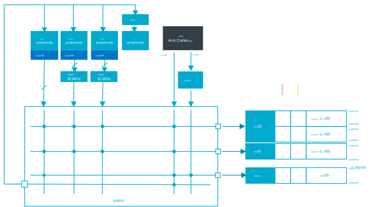
See Block diagram, AMBA interconnect (AMBIX), and EasyDMA for more information about the AMBIX interconnects and EasyDMA.
RAM — Random access memory
The device RAM has regions arranged in one contiguous memory range, accessible from both the CPU and peripherals.
Each RAM region has separate power control for System ON and System OFF mode. This preserves RAM contents in sleep modes or powers off RAM to save power. The sections are illustrated in Memory layout, and the register interface is described in MEMCONF — Memory configuration.
NVM — Non-volatile memory
The CPU can read from non-volatile memory (RRAM) an unlimited number of times, but is restricted in how it writes to memory and the number of writes it can perform.
Writing to RRAM is managed by the RRAM controller (RRAMC), see RRAMC — Resistive random access memory controller.
The Arm® Cortex®-M33 CPU can access RRAM using the C-AHB (code) bus as shown in Memory layout. The code bus (C-AHB) interface is used for any instruction fetch or data access fetch to the code region of the Arm memory model. C-AHB bus access is cached, see CACHE — Instruction/data cache.
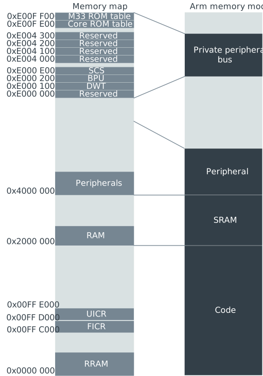
Memory map
The complete memory map is shown in the following figure.
Instantiation
| ID | Base address | Instance | Description |
|---|---|---|---|
| 66 | 0x40042000 | DPPIC00 | DPPI controller DPPIC00 |
| 68 | 0x40044000 | PPIB00 | PPI bridge PPIB00 |
| 69 | 0x40045000 | PPIB01 | PPI bridge PPIB01 |
| 74 | 0x4004A000 | AAR00 | Accelerated address resolver 00 |
| 74 | 0x4004A000 | CCM00 | AES CCM mode encryption CCM00, running of HCLKCORE |
| 75 | 0x4004B000 | ECB00 | AES ECB mode encryption 00 |
| 78 | 0x4004E000 | RRAMC | RRAM Non-Volatile Memory Controller |
| 82 | 0x40052000 | CTRLAP | Control access port CPU side |
| 83 | 0x40053000 | TAD | Trace and debug control |
| 85 | 0x40055000 | TIMER00 | Timer TIMER00 |
| 88 | 0x40058000 | EGU00 | Event generator unit EGU00 |
| 89 | 0x40059000 | CRACEN | True Random Number Generator |
| 89 | 0x40059000 | CRACENCORE | True Random Number Generator |
| 130 | 0x40082000 | DPPIC10 | DPPI controller DPPIC10 |
| 131 | 0x40083000 | PPIB10 | PPI bridge PPIB10 |
| 132 | 0x40084000 | PPIB11 | PPI bridge PPIB11 |
| 133 | 0x40085000 | TIMER10 | Timer TIMER10 |
| 135 | 0x40087000 | EGU10 | Event generator unit EGU10 |
| 138 | 0x4008A000 | RADIO | 2.4 GHz radio RADIO |
| 194 | 0x400C2000 | DPPIC20 | DPPI controller DPPIC20 |
| 195 | 0x400C3000 | PPIB20 | PPI bridge PPIB20 |
| 196 | 0x400C4000 | PPIB21 | PPI bridge PPIB21 |
| 197 | 0x400C5000 | PPIB22 | PPI bridge PPIB22 |
| 198 | 0x400C6000 | SPIM20 | SPI controller SPIM20 |
| 198 | 0x400C6000 | SPIS20 | SPI peripheral SPIS20 |
| 198 | 0x400C6000 | TWIM20 | Two-wire interface controller TWIM20 |
| 198 | 0x400C6000 | TWIS20 | Two-wire interface target TWIS20 |
| 198 | 0x400C6000 | UARTE20 | Universal asynchronous receiver/transmitter UARTE20 |
| 199 | 0x400C7000 | SPIM21 | SPI controller SPIM21 |
| 199 | 0x400C7000 | SPIS21 | SPI peripheral SPIS21 |
| 199 | 0x400C7000 | TWIM21 | Two-wire interface controller TWIM21 |
| 199 | 0x400C7000 | TWIS21 | Two-wire interface target TWIS21 |
| 199 | 0x400C7000 | UARTE21 | Universal asynchronous receiver/transmitter UARTE21 |
| 200 | 0x400C8000 | SPIM22 | SPI controller SPIM22 |
| 200 | 0x400C8000 | SPIS22 | SPI peripheral SPIS22 |
| 200 | 0x400C8000 | TWIM22 | Two-wire interface controller TWIM22 |
| 200 | 0x400C8000 | TWIS22 | Two-wire interface target TWIS22 |
| 200 | 0x400C8000 | UARTE22 | Universal asynchronous receiver/transmitter UARTE22 |
| 201 | 0x400C9000 | EGU20 | Event generator unit EGU20 |
| 202 | 0x400CA000 | TIMER20 | Timer TIMER20 |
| 207 | 0x400CF000 | MEMCONF | Memory Configuration MEMCONF |
| 210 | 0x400D2000 | PWM20 | Pulse width modulation unit PWM20 |
| 213 | 0x400D5000 | SAADC | Successive approximation analog-to-digital converter SAADC |
| 215 | 0x400D7000 | TEMP | Temperature sensor TEMP |
| 216 | 0x400D8200 | P1 | General purpose input and output, port P1 |
| 218 | 0x400DA000 | GPIOTE20 | 8 channels and 1 interrupts for GPIO port P1 GPIO tasks and events GPIOTE20 |
| 224 | 0x400E0000 | QDEC20 | Quadrature decoder QDEC20 |
| 226 | 0x400E2000 | GRTC | Global RTC GRTC |
| 239 | 0x400EF000 | TAMPC | Tamper controller TAMPC |
| 258 | 0x40102000 | DPPIC30 | DPPI controller DPPIC30 |
| 259 | 0x40103000 | PPIB30 | PPI bridge PPIB30 |
| 264 | 0x40108000 | WDT30 | Watchdog timer WDT30 |
| 266 | 0x4010A000 | P0 | General purpose input and output, port P0 |
| 268 | 0x4010C000 | GPIOTE30 | 4 channels and 1 interrupts for GPIO port P0 GPIO tasks and events GPIOTE30 |
| 270 | 0x4010E000 | CLOCK | Clock control |
| 270 | 0x4010E000 | POWER | Power control |
| 270 | 0x4010E000 | RESET | Reset status |
| 288 | 0x40120000 | OSCILLATORS | Oscillator control |
| 288 | 0x40120000 | REGULATORS | Regulator control |
| N/A | 0x00FFC000 | FICR | Factory information configuration |
| N/A | 0x00FFD000 | UICR | User information configuration |