REGULATORS — Regulator control
The power supply consists of a number of LDO and DC/DC regulators that maximize the system's power efficiency.
All system components are powered from the main on-chip voltage regulator, VREGMAIN. The regulator converts the voltage supplied on VDD to internal voltage.
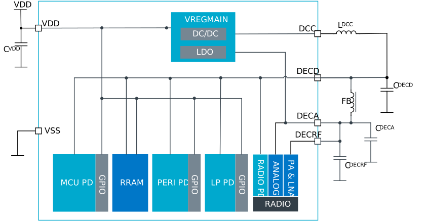
The main supply voltage is connected to the VDD pin.
VREGMAIN — Main regulator
VREGMAIN is the main regulator of the system.
The device only supports DC/DC mode, which needs external components. For details, see Reference circuitry.
VREGMAIN starts up using a fall-back mode, and the DC/DC regulator must be enabled using register VREGMAIN.DCDCEN.
Inductor detection
The DC/DC regulator requires an external inductor connected to the DCC pin. If an inductor is not present, the regulator stays in fall-back mode to enable a soft shut-down of the system. Register VREGMAIN.INDUCTORDET reports the inductor detection status and can be used to detect inductor failures that prevent DC/DC operation.
Registers
Instances
| Instance | Domain | Base address | Description |
|---|---|---|---|
| REGULATORS | GLOBAL | 0x40120000 | Regulator control |
Register overview
| Register | Offset | Description |
|---|---|---|
| SYSTEMOFF | 0x500 | System OFF register |
| POFCON | 0x530 | Power-fail comparator configuration This register is retained. |
| POFSTAT | 0x534 | Power-fail comparator status register |
| VREGMAIN.DCDCEN | 0x600 | Enable DC/DC converter |
| VREGMAIN.INDUCTORDET | 0x604 | VREGMAIN inductor detection |
SYSTEMOFF
Address offset: 0x500
System OFF register
| Bit number | 31 | 30 | 29 | 28 | 27 | 26 | 25 | 24 | 23 | 22 | 21 | 20 | 19 | 18 | 17 | 16 | 15 | 14 | 13 | 12 | 11 | 10 | 9 | 8 | 7 | 6 | 5 | 4 | 3 | 2 | 1 | 0 | |||
|---|---|---|---|---|---|---|---|---|---|---|---|---|---|---|---|---|---|---|---|---|---|---|---|---|---|---|---|---|---|---|---|---|---|---|---|
| ID | A | ||||||||||||||||||||||||||||||||||
| Reset 0x00000000 | 0 | 0 | 0 | 0 | 0 | 0 | 0 | 0 | 0 | 0 | 0 | 0 | 0 | 0 | 0 | 0 | 0 | 0 | 0 | 0 | 0 | 0 | 0 | 0 | 0 | 0 | 0 | 0 | 0 | 0 | 0 | 0 | |||
| ID | R/W | Field | Value ID | Value | Description | ||||||||||||||||||||||||||||||
| A | W | SYSTEMOFF | Enable System OFF mode | ||||||||||||||||||||||||||||||||
Enter | 1 | Enable System OFF mode | |||||||||||||||||||||||||||||||||
POFCON (Retained)
Address offset: 0x530
Power-fail comparator configuration
This register is retained.
| Bit number | 31 | 30 | 29 | 28 | 27 | 26 | 25 | 24 | 23 | 22 | 21 | 20 | 19 | 18 | 17 | 16 | 15 | 14 | 13 | 12 | 11 | 10 | 9 | 8 | 7 | 6 | 5 | 4 | 3 | 2 | 1 | 0 | |||
|---|---|---|---|---|---|---|---|---|---|---|---|---|---|---|---|---|---|---|---|---|---|---|---|---|---|---|---|---|---|---|---|---|---|---|---|
| ID | C | B | B | B | B | A | |||||||||||||||||||||||||||||
| Reset 0x00000000 | 0 | 0 | 0 | 0 | 0 | 0 | 0 | 0 | 0 | 0 | 0 | 0 | 0 | 0 | 0 | 0 | 0 | 0 | 0 | 0 | 0 | 0 | 0 | 0 | 0 | 0 | 0 | 0 | 0 | 0 | 0 | 0 | |||
| ID | R/W | Field | Value ID | Value | Description | ||||||||||||||||||||||||||||||
| A | RW | POF | Enable or disable power-fail comparator | ||||||||||||||||||||||||||||||||
Disabled | 0 | Disable | |||||||||||||||||||||||||||||||||
Enabled | 1 | Enable | |||||||||||||||||||||||||||||||||
| B | RW | THRESHOLD | Power-fail comparator threshold setting | ||||||||||||||||||||||||||||||||
V17 | 0 | Set threshold to 1.7 V for VDD | |||||||||||||||||||||||||||||||||
V18 | 1 | Set threshold to 1.8 V for VDD | |||||||||||||||||||||||||||||||||
V19 | 2 | Set threshold to 1.9 V for VDD | |||||||||||||||||||||||||||||||||
V20 | 3 | Set threshold to 2.0 V for VDD | |||||||||||||||||||||||||||||||||
V21 | 4 | Set threshold to 2.1 V for VDD | |||||||||||||||||||||||||||||||||
V22 | 5 | Set threshold to 2.2 V for VDD | |||||||||||||||||||||||||||||||||
V23 | 6 | Set threshold to 2.3 V for VDD | |||||||||||||||||||||||||||||||||
V24 | 7 | Set threshold to 2.4 V for VDD | |||||||||||||||||||||||||||||||||
V25 | 8 | Set threshold to 2.5 V for VDD | |||||||||||||||||||||||||||||||||
V26 | 9 | Set threshold to 2.6 V for VDD | |||||||||||||||||||||||||||||||||
V27 | 10 | Set threshold to 2.7 V for VDD | |||||||||||||||||||||||||||||||||
V28 | 11 | Set threshold to 2.8 V for VDD | |||||||||||||||||||||||||||||||||
V29 | 12 | Set threshold to 2.9 V for VDD | |||||||||||||||||||||||||||||||||
V30 | 13 | Set threshold to 3.0 V for VDD | |||||||||||||||||||||||||||||||||
V31 | 14 | Set threshold to 3.1 V for VDD | |||||||||||||||||||||||||||||||||
V32 | 15 | Set threshold to 3.2 V for VDD | |||||||||||||||||||||||||||||||||
| C | RW | EVENTDISABLE | Disable the POFWARN power-fail warning event | ||||||||||||||||||||||||||||||||
Enabled | 0 | POFWARN event is generated | |||||||||||||||||||||||||||||||||
Disabled | 1 | POFWARN event is not generated | |||||||||||||||||||||||||||||||||
POFSTAT
Address offset: 0x534
Power-fail comparator status register
| Bit number | 31 | 30 | 29 | 28 | 27 | 26 | 25 | 24 | 23 | 22 | 21 | 20 | 19 | 18 | 17 | 16 | 15 | 14 | 13 | 12 | 11 | 10 | 9 | 8 | 7 | 6 | 5 | 4 | 3 | 2 | 1 | 0 | |||
|---|---|---|---|---|---|---|---|---|---|---|---|---|---|---|---|---|---|---|---|---|---|---|---|---|---|---|---|---|---|---|---|---|---|---|---|
| ID | A | ||||||||||||||||||||||||||||||||||
| Reset 0x00000000 | 0 | 0 | 0 | 0 | 0 | 0 | 0 | 0 | 0 | 0 | 0 | 0 | 0 | 0 | 0 | 0 | 0 | 0 | 0 | 0 | 0 | 0 | 0 | 0 | 0 | 0 | 0 | 0 | 0 | 0 | 0 | 0 | |||
| ID | R/W | Field | Value ID | Value | Description | ||||||||||||||||||||||||||||||
| A | R | COMPARATOR | Power-fail comparator status | ||||||||||||||||||||||||||||||||
Above | 0 | Voltage detected above VPOF threshold | |||||||||||||||||||||||||||||||||
Below | 1 | Voltage detected below VPOF threshold | |||||||||||||||||||||||||||||||||
VREGMAIN
Register interface for main voltage regulator.
VREGMAIN.DCDCEN
Address offset: 0x600
Enable DC/DC converter
| Bit number | 31 | 30 | 29 | 28 | 27 | 26 | 25 | 24 | 23 | 22 | 21 | 20 | 19 | 18 | 17 | 16 | 15 | 14 | 13 | 12 | 11 | 10 | 9 | 8 | 7 | 6 | 5 | 4 | 3 | 2 | 1 | 0 | |||
|---|---|---|---|---|---|---|---|---|---|---|---|---|---|---|---|---|---|---|---|---|---|---|---|---|---|---|---|---|---|---|---|---|---|---|---|
| ID | A | ||||||||||||||||||||||||||||||||||
| Reset 0x00000000 | 0 | 0 | 0 | 0 | 0 | 0 | 0 | 0 | 0 | 0 | 0 | 0 | 0 | 0 | 0 | 0 | 0 | 0 | 0 | 0 | 0 | 0 | 0 | 0 | 0 | 0 | 0 | 0 | 0 | 0 | 0 | 0 | |||
| ID | R/W | Field | Value ID | Value | Description | ||||||||||||||||||||||||||||||
| A | RW | VAL | Enable DC/DC buck converter | ||||||||||||||||||||||||||||||||
Disabled | 0 | Disable DC/DC buck converter | |||||||||||||||||||||||||||||||||
Enabled | 1 | Enable DC/DC converter If inductor is not present (see register VREGMAIN.INDUCTORDET), the DC/DC converter cannot operate | |||||||||||||||||||||||||||||||||
VREGMAIN.INDUCTORDET
Address offset: 0x604
VREGMAIN inductor detection
Ensure that an inductor is connected to the DCC pin. The detection can only take place before the DC/DC converter is enabled.
Note: The DC/DC converter cannot operate without an inductor.
| Bit number | 31 | 30 | 29 | 28 | 27 | 26 | 25 | 24 | 23 | 22 | 21 | 20 | 19 | 18 | 17 | 16 | 15 | 14 | 13 | 12 | 11 | 10 | 9 | 8 | 7 | 6 | 5 | 4 | 3 | 2 | 1 | 0 | |||
|---|---|---|---|---|---|---|---|---|---|---|---|---|---|---|---|---|---|---|---|---|---|---|---|---|---|---|---|---|---|---|---|---|---|---|---|
| ID | A | ||||||||||||||||||||||||||||||||||
| Reset 0x00000000 | 0 | 0 | 0 | 0 | 0 | 0 | 0 | 0 | 0 | 0 | 0 | 0 | 0 | 0 | 0 | 0 | 0 | 0 | 0 | 0 | 0 | 0 | 0 | 0 | 0 | 0 | 0 | 0 | 0 | 0 | 0 | 0 | |||
| ID | R/W | Field | Value ID | Value | Description | ||||||||||||||||||||||||||||||
| A | R | DETECTED | |||||||||||||||||||||||||||||||||
InductorNotDetected | 0 | VREGMAIN inductor not detected | |||||||||||||||||||||||||||||||||
InductorDetected | 1 | VREGMAIN inductor detected | |||||||||||||||||||||||||||||||||