TAMPC — Tamper controller
The tamper controller peripheral handles input from internal and external physical attack detectors and controls the device response.
The following figure shows an overview of the TAMPC detectors, input, and output.
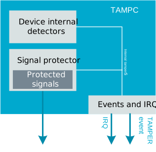
- Detection of fault injection attacks (voltage glitching, electromagnetic fault
injection, etc.)
- Signal protector to guard critical configuration signals
- Glitch detectors to detect timing violations of internal logic
Internal tamper detectors
A tamper attack detected by any of the internal tamper detectors indicates that the device's internal logic could be affected by the attack, and the system state could be compromised.
Glitch detector
The device implements general detectors to prevent fault injection attacks.
Detectors are strategically placed among the digital logic to detect local timing glitches (timing violations). The glitch detectors monitor the effects of attempted fault injection attacks and not the attack attempt itself. For example, fault injection attempts could be utilizing voltage glitches on supply or decoupling pins, or electro magnetic fault injection (EMFI) techniques. The detectors are designed and tuned to be more sensitive to timing violations than normal logic, enabling the digital logic to react before an injected fault is propagated through the system.
The glitch detectors are enabled from reset and can be disabled for debugging using the registers PROTECT.GLITCHSLOWDOMAIN.CTRL and PROTECT.GLITCHFASTDOMAIN.CTRL.
- A TAMPC EVENT is generated.
- A chip reset is triggered and the SECTAMPER value in the reset reason register indicates what happened, depending on the status of the register PROTECT.INTRESETEN.CTRL.
Signal protector
The device implements detectors to protect selected signals that control critical device features.
- A TAMPC event is generated.
- A chip reset is triggered and the SECTAMPER value in the reset reason register indicates what happened, depending on the status of the register PROTECT.INTRESETEN.CTRL.
The INTRESETEN register is enabled from reset. The PROTECT.<component>.STATUS registers indicate which protected signal had an unintentional value change when the register INTENRESETEN is disabled.
- Initial register write to clear the write protection.
- Register write to change the signal's value.
Write Clear to the WRITEPROTECTION field in the PROTECT.<component>.CTRL register to clear the write protection in the first register write. Then write to the VALUE and LOCK fields in the next register write operation.
The write protection is automatically re-enabled after the subsequent write to change the VALUE field when the register write does not include the Clear value in the WRITEPROTECTION field.
The LOCK field controls a lock feature which prevents further updates to the VALUE and LOCK fields until a reset with the required reset source for the specific signal is issued.
- Register write does not have the correct write key
- Write protection is active and the write operation does not contain the value to clear the write protection
- The lock is enabled
- Write Clear to the WRITEPROTECTION field and KEY to the KEY field.
- Write Disabled to the WRITEPROTECTION field, KEY to the KEY field, and KEY to the desired LOCK and VALUE fields.
Debugger signals
TAMPC provides protection for the following Arm® CoreSight™ debugger signals.
| Signal | Name | Notes |
|---|---|---|
| NIDEN | Non-Invasive Debug Enable | ETM/ITM trace and other non-halting debug methods |
| DBGEN | Invasive Debug Enable | The debugger may halt the CPU for debug purposes |
For more information about using the protected debugger signals, see Debug.
TAMPC reset behavior
TAMPC registers are reset by different sources.
- Category 1 – Brownout reset, power-on reset
- Category 2 – Pin reset and TAMPC reset
- Category 3 – Watchdog timer reset, CPU lockup reset, System reset request, and Wake-up from System OFF reset
| Reset source | |||||
|---|---|---|---|---|---|
| Register | Function | Reset value | Cat 1 | Cat 2 | Cat 3 |
| PROTECT.DOMAIN[0].DBGEN | Allow invasive debugging. | 0 | x | x | |
| PROTECT.DOMAIN[0].NIDEN | Allow non-invasive debugging. | 0 | x | x | |
| PROTECT.GLITCHSLOWDOMAIN | Enable slow domain glitch detector. | 1 | x | x | x |
| PROTECT.GLITCHFASTDOMAIN | Enable fast domain glitch detector. | 1 | x | x | x |
| PROTECT.EXTRESETEN | Enable automatic reset from external tamper detectors events. | 0 | x | x | x |
| PROTECT.INTRESETEN | Enable automatic reset from internal tamper detector events. | 1 | x | x | x |
| PROTECT.ERASEPROTECT | Allow device erase using CTRL-AP and RRAMC. | 0 | x | x | x |
Registers
Instances
| Instance | Domain | Base address | Description |
|---|---|---|---|
| TAMPC | GLOBAL | 0x400EF000 | Tamper controller TAMPC |
Configuration
| Instance | Domain | Configuration |
|---|---|---|
| TAMPC | GLOBAL | Device can use SWD pins as GPIO pins. Reset value of field VALUE in register PROTECT.INTRESETEN.CTRL: 1 |
Register overview
| Register | Offset | Description |
|---|---|---|
| EVENTS_TAMPER | 0x100 | Tamper controller detected an error. |
| EVENTS_WRITEERROR | 0x104 | Attempt to write a VALUE in PROTECT registers without clearing the WRITEPROTECT. |
| INTEN | 0x300 | Enable or disable interrupt |
| INTENSET | 0x304 | Enable interrupt |
| INTENCLR | 0x308 | Disable interrupt |
| INTPEND | 0x30C | Pending interrupts |
| STATUS | 0x400 | The tamper controller status. |
| PROTECT.DOMAIN[n].DBGEN.CTRL | 0x500 | Control register for invasive (halting) debug enable for the local debug components within domain n. |
| PROTECT.DOMAIN[n].DBGEN.STATUS | 0x504 | Status register for invasive (halting) debug enable for domain n. |
| PROTECT.DOMAIN[n].NIDEN.CTRL | 0x508 | Control register for non-invasive debug enable for the local debug components within domain n. |
| PROTECT.DOMAIN[n].NIDEN.STATUS | 0x50C | Status register for non-invasive debug enable for domain n. |
| PROTECT.AP[n].DBGEN.CTRL | 0x700 | Control register to enable invasive (halting) debug in domain ns access port. |
| PROTECT.AP[n].DBGEN.STATUS | 0x704 | Status register for invasive (halting) debug enable for domain ns access port. |
| PROTECT.GPIOSWD.CTRL | 0x878 | Control register for activating GPIO functionality. |
| PROTECT.GPIOSWD.STATUS | 0x87C | Status register for active shield detector enable signal. |
| PROTECT.GLITCHSLOWDOMAIN.CTRL | 0x940 | Control register for slow domain glitch detectors enable signal. |
| PROTECT.GLITCHSLOWDOMAIN.STATUS | 0x944 | Status register for slow domain glitch detectors enable signal. |
| PROTECT.GLITCHFASTDOMAIN.CTRL | 0x948 | Control register for fast domain glitch detectors enable signal. |
| PROTECT.GLITCHFASTDOMAIN.STATUS | 0x94C | Status register for fast domain glitch detectors enable signal. |
| PROTECT.INTRESETEN.CTRL | 0x978 | Control register for internal tamper reset enable signal. |
| PROTECT.INTRESETEN.STATUS | 0x97C | Status register for internal tamper reset enable signal. |
| PROTECT.ERASEPROTECT.CTRL | 0x980 | Control register for erase protection. |
| PROTECT.ERASEPROTECT.STATUS | 0x984 | Status register for eraseprotect. |
EVENTS_TAMPER
Address offset: 0x100
Tamper controller detected an error.
| Bit number | 31 | 30 | 29 | 28 | 27 | 26 | 25 | 24 | 23 | 22 | 21 | 20 | 19 | 18 | 17 | 16 | 15 | 14 | 13 | 12 | 11 | 10 | 9 | 8 | 7 | 6 | 5 | 4 | 3 | 2 | 1 | 0 | |||
|---|---|---|---|---|---|---|---|---|---|---|---|---|---|---|---|---|---|---|---|---|---|---|---|---|---|---|---|---|---|---|---|---|---|---|---|
| ID | A | ||||||||||||||||||||||||||||||||||
| Reset 0x00000000 | 0 | 0 | 0 | 0 | 0 | 0 | 0 | 0 | 0 | 0 | 0 | 0 | 0 | 0 | 0 | 0 | 0 | 0 | 0 | 0 | 0 | 0 | 0 | 0 | 0 | 0 | 0 | 0 | 0 | 0 | 0 | 0 | |||
| ID | R/W | Field | Value ID | Value | Description | ||||||||||||||||||||||||||||||
| A | RW | EVENTS_TAMPER | Tamper controller detected an error. | ||||||||||||||||||||||||||||||||
NotGenerated | 0 | Event not generated | |||||||||||||||||||||||||||||||||
Generated | 1 | Event generated | |||||||||||||||||||||||||||||||||
EVENTS_WRITEERROR
Address offset: 0x104
Attempt to write a VALUE in PROTECT registers without clearing the WRITEPROTECT.
| Bit number | 31 | 30 | 29 | 28 | 27 | 26 | 25 | 24 | 23 | 22 | 21 | 20 | 19 | 18 | 17 | 16 | 15 | 14 | 13 | 12 | 11 | 10 | 9 | 8 | 7 | 6 | 5 | 4 | 3 | 2 | 1 | 0 | |||
|---|---|---|---|---|---|---|---|---|---|---|---|---|---|---|---|---|---|---|---|---|---|---|---|---|---|---|---|---|---|---|---|---|---|---|---|
| ID | A | ||||||||||||||||||||||||||||||||||
| Reset 0x00000000 | 0 | 0 | 0 | 0 | 0 | 0 | 0 | 0 | 0 | 0 | 0 | 0 | 0 | 0 | 0 | 0 | 0 | 0 | 0 | 0 | 0 | 0 | 0 | 0 | 0 | 0 | 0 | 0 | 0 | 0 | 0 | 0 | |||
| ID | R/W | Field | Value ID | Value | Description | ||||||||||||||||||||||||||||||
| A | RW | EVENTS_WRITEERROR | Attempt to write a VALUE in PROTECT registers without clearing the WRITEPROTECT. | ||||||||||||||||||||||||||||||||
NotGenerated | 0 | Event not generated | |||||||||||||||||||||||||||||||||
Generated | 1 | Event generated | |||||||||||||||||||||||||||||||||
INTEN
Address offset: 0x300
Enable or disable interrupt
| Bit number | 31 | 30 | 29 | 28 | 27 | 26 | 25 | 24 | 23 | 22 | 21 | 20 | 19 | 18 | 17 | 16 | 15 | 14 | 13 | 12 | 11 | 10 | 9 | 8 | 7 | 6 | 5 | 4 | 3 | 2 | 1 | 0 | |||
|---|---|---|---|---|---|---|---|---|---|---|---|---|---|---|---|---|---|---|---|---|---|---|---|---|---|---|---|---|---|---|---|---|---|---|---|
| ID | B | A | |||||||||||||||||||||||||||||||||
| Reset 0x00000000 | 0 | 0 | 0 | 0 | 0 | 0 | 0 | 0 | 0 | 0 | 0 | 0 | 0 | 0 | 0 | 0 | 0 | 0 | 0 | 0 | 0 | 0 | 0 | 0 | 0 | 0 | 0 | 0 | 0 | 0 | 0 | 0 | |||
| ID | R/W | Field | Value ID | Value | Description | ||||||||||||||||||||||||||||||
| A | RW | TAMPER | Enable or disable interrupt for event TAMPER | ||||||||||||||||||||||||||||||||
Disabled | 0 | Disable | |||||||||||||||||||||||||||||||||
Enabled | 1 | Enable | |||||||||||||||||||||||||||||||||
| B | RW | WRITEERROR | Enable or disable interrupt for event WRITEERROR | ||||||||||||||||||||||||||||||||
Disabled | 0 | Disable | |||||||||||||||||||||||||||||||||
Enabled | 1 | Enable | |||||||||||||||||||||||||||||||||
INTENSET
Address offset: 0x304
Enable interrupt
| Bit number | 31 | 30 | 29 | 28 | 27 | 26 | 25 | 24 | 23 | 22 | 21 | 20 | 19 | 18 | 17 | 16 | 15 | 14 | 13 | 12 | 11 | 10 | 9 | 8 | 7 | 6 | 5 | 4 | 3 | 2 | 1 | 0 | |||
|---|---|---|---|---|---|---|---|---|---|---|---|---|---|---|---|---|---|---|---|---|---|---|---|---|---|---|---|---|---|---|---|---|---|---|---|
| ID | B | A | |||||||||||||||||||||||||||||||||
| Reset 0x00000000 | 0 | 0 | 0 | 0 | 0 | 0 | 0 | 0 | 0 | 0 | 0 | 0 | 0 | 0 | 0 | 0 | 0 | 0 | 0 | 0 | 0 | 0 | 0 | 0 | 0 | 0 | 0 | 0 | 0 | 0 | 0 | 0 | |||
| ID | R/W | Field | Value ID | Value | Description | ||||||||||||||||||||||||||||||
| A | RW | TAMPER | Write '1' to enable interrupt for event TAMPER | ||||||||||||||||||||||||||||||||
Set | 1 | Enable | |||||||||||||||||||||||||||||||||
Disabled | 0 | Read: Disabled | |||||||||||||||||||||||||||||||||
Enabled | 1 | Read: Enabled | |||||||||||||||||||||||||||||||||
| B | RW | WRITEERROR | Write '1' to enable interrupt for event WRITEERROR | ||||||||||||||||||||||||||||||||
Set | 1 | Enable | |||||||||||||||||||||||||||||||||
Disabled | 0 | Read: Disabled | |||||||||||||||||||||||||||||||||
Enabled | 1 | Read: Enabled | |||||||||||||||||||||||||||||||||
INTENCLR
Address offset: 0x308
Disable interrupt
| Bit number | 31 | 30 | 29 | 28 | 27 | 26 | 25 | 24 | 23 | 22 | 21 | 20 | 19 | 18 | 17 | 16 | 15 | 14 | 13 | 12 | 11 | 10 | 9 | 8 | 7 | 6 | 5 | 4 | 3 | 2 | 1 | 0 | |||
|---|---|---|---|---|---|---|---|---|---|---|---|---|---|---|---|---|---|---|---|---|---|---|---|---|---|---|---|---|---|---|---|---|---|---|---|
| ID | B | A | |||||||||||||||||||||||||||||||||
| Reset 0x00000000 | 0 | 0 | 0 | 0 | 0 | 0 | 0 | 0 | 0 | 0 | 0 | 0 | 0 | 0 | 0 | 0 | 0 | 0 | 0 | 0 | 0 | 0 | 0 | 0 | 0 | 0 | 0 | 0 | 0 | 0 | 0 | 0 | |||
| ID | R/W | Field | Value ID | Value | Description | ||||||||||||||||||||||||||||||
| A | RW | TAMPER | Write '1' to disable interrupt for event TAMPER | ||||||||||||||||||||||||||||||||
Clear | 1 | Disable | |||||||||||||||||||||||||||||||||
Disabled | 0 | Read: Disabled | |||||||||||||||||||||||||||||||||
Enabled | 1 | Read: Enabled | |||||||||||||||||||||||||||||||||
| B | RW | WRITEERROR | Write '1' to disable interrupt for event WRITEERROR | ||||||||||||||||||||||||||||||||
Clear | 1 | Disable | |||||||||||||||||||||||||||||||||
Disabled | 0 | Read: Disabled | |||||||||||||||||||||||||||||||||
Enabled | 1 | Read: Enabled | |||||||||||||||||||||||||||||||||
INTPEND
Address offset: 0x30C
Pending interrupts
| Bit number | 31 | 30 | 29 | 28 | 27 | 26 | 25 | 24 | 23 | 22 | 21 | 20 | 19 | 18 | 17 | 16 | 15 | 14 | 13 | 12 | 11 | 10 | 9 | 8 | 7 | 6 | 5 | 4 | 3 | 2 | 1 | 0 | |||
|---|---|---|---|---|---|---|---|---|---|---|---|---|---|---|---|---|---|---|---|---|---|---|---|---|---|---|---|---|---|---|---|---|---|---|---|
| ID | B | A | |||||||||||||||||||||||||||||||||
| Reset 0x00000000 | 0 | 0 | 0 | 0 | 0 | 0 | 0 | 0 | 0 | 0 | 0 | 0 | 0 | 0 | 0 | 0 | 0 | 0 | 0 | 0 | 0 | 0 | 0 | 0 | 0 | 0 | 0 | 0 | 0 | 0 | 0 | 0 | |||
| ID | R/W | Field | Value ID | Value | Description | ||||||||||||||||||||||||||||||
| A | R | TAMPER | Read pending status of interrupt for event TAMPER | ||||||||||||||||||||||||||||||||
NotPending | 0 | Read: Not pending | |||||||||||||||||||||||||||||||||
Pending | 1 | Read: Pending | |||||||||||||||||||||||||||||||||
| B | R | WRITEERROR | Read pending status of interrupt for event WRITEERROR | ||||||||||||||||||||||||||||||||
NotPending | 0 | Read: Not pending | |||||||||||||||||||||||||||||||||
Pending | 1 | Read: Pending | |||||||||||||||||||||||||||||||||
STATUS
Address offset: 0x400
The tamper controller status.
| Bit number | 31 | 30 | 29 | 28 | 27 | 26 | 25 | 24 | 23 | 22 | 21 | 20 | 19 | 18 | 17 | 16 | 15 | 14 | 13 | 12 | 11 | 10 | 9 | 8 | 7 | 6 | 5 | 4 | 3 | 2 | 1 | 0 | |||
|---|---|---|---|---|---|---|---|---|---|---|---|---|---|---|---|---|---|---|---|---|---|---|---|---|---|---|---|---|---|---|---|---|---|---|---|
| ID | F | E | D | C | B | A | |||||||||||||||||||||||||||||
| Reset 0x00000000 | 0 | 0 | 0 | 0 | 0 | 0 | 0 | 0 | 0 | 0 | 0 | 0 | 0 | 0 | 0 | 0 | 0 | 0 | 0 | 0 | 0 | 0 | 0 | 0 | 0 | 0 | 0 | 0 | 0 | 0 | 0 | 0 | |||
| ID | R/W | Field | Value ID | Value | Description | ||||||||||||||||||||||||||||||
| A | RW | PROTECT | Error detected for the protected signals. | ||||||||||||||||||||||||||||||||
NotDetected | 0 | Not detected. | |||||||||||||||||||||||||||||||||
Detected | 1 | Detected. | |||||||||||||||||||||||||||||||||
| B | RW | GLITCHSLOWDOMAIN[i] (i=0..0) | Slow domain glitch detector i detected an error. | ||||||||||||||||||||||||||||||||
NotDetected | 0 | Not detected. | |||||||||||||||||||||||||||||||||
Detected | 1 | Detected. | |||||||||||||||||||||||||||||||||
| C-F | RW | GLITCHFASTDOMAIN[i] (i=0..3) | Fast domain glitch detector i detected an error. | ||||||||||||||||||||||||||||||||
NotDetected | 0 | Not detected. | |||||||||||||||||||||||||||||||||
Detected | 1 | Detected. | |||||||||||||||||||||||||||||||||
PROTECT.DOMAIN[n].DBGEN.CTRL
Address offset: 0x500 + (n × 0x20)
Control register for invasive (halting) debug enable for the local debug components within domain n.
| Bit number | 31 | 30 | 29 | 28 | 27 | 26 | 25 | 24 | 23 | 22 | 21 | 20 | 19 | 18 | 17 | 16 | 15 | 14 | 13 | 12 | 11 | 10 | 9 | 8 | 7 | 6 | 5 | 4 | 3 | 2 | 1 | 0 | |||
|---|---|---|---|---|---|---|---|---|---|---|---|---|---|---|---|---|---|---|---|---|---|---|---|---|---|---|---|---|---|---|---|---|---|---|---|
| ID | D | D | D | D | D | D | D | D | D | D | D | D | D | D | D | D | C | C | C | C | B | A | |||||||||||||
| Reset 0x00000010 | 0 | 0 | 0 | 0 | 0 | 0 | 0 | 0 | 0 | 0 | 0 | 0 | 0 | 0 | 0 | 0 | 0 | 0 | 0 | 0 | 0 | 0 | 0 | 0 | 0 | 0 | 0 | 1 | 0 | 0 | 0 | 0 | |||
| ID | R/W | Field | Value ID | Value | Description | ||||||||||||||||||||||||||||||
| A | RW | VALUE | Set value of dbgen signal. | ||||||||||||||||||||||||||||||||
Low | 0 | Signal is logic 0, indicating that invasive debug is disabled. | |||||||||||||||||||||||||||||||||
High | 1 | Signal is logic 1, indicating that invasive debug is enabled. | |||||||||||||||||||||||||||||||||
| B | W1 | LOCK | Lock this register to prevent changes to the VALUE field until next reset. | ||||||||||||||||||||||||||||||||
Disabled | 0 | Lock disabled. | |||||||||||||||||||||||||||||||||
Enabled | 1 | Lock enabled. | |||||||||||||||||||||||||||||||||
| C | RW | WRITEPROTECTION | The write protection must be cleared to allow updates to the VALUE field. The write protection is cleared by writing CLEAR in a separate write operation prior to updating the VALUE and LOCK fields. The write protection is automatically enabled after the corresponding change to the VALUE field. | ||||||||||||||||||||||||||||||||
Disabled | 0x0 | Read: Write protection is disabled. | |||||||||||||||||||||||||||||||||
Enabled | 0x1 | Read: Write protection is enabled. | |||||||||||||||||||||||||||||||||
Clear | 0xF | Write: Value to clear write protection. | |||||||||||||||||||||||||||||||||
| D | W | KEY | Required write key for upper 16 bits. Must be included in all register write operations. | ||||||||||||||||||||||||||||||||
KEY | 0x50FA | Write key value. | |||||||||||||||||||||||||||||||||
PROTECT.DOMAIN[n].DBGEN.STATUS
Address offset: 0x504 + (n × 0x20)
Status register for invasive (halting) debug enable for domain n.
| Bit number | 31 | 30 | 29 | 28 | 27 | 26 | 25 | 24 | 23 | 22 | 21 | 20 | 19 | 18 | 17 | 16 | 15 | 14 | 13 | 12 | 11 | 10 | 9 | 8 | 7 | 6 | 5 | 4 | 3 | 2 | 1 | 0 | |||
|---|---|---|---|---|---|---|---|---|---|---|---|---|---|---|---|---|---|---|---|---|---|---|---|---|---|---|---|---|---|---|---|---|---|---|---|
| ID | A | ||||||||||||||||||||||||||||||||||
| Reset 0x00000000 | 0 | 0 | 0 | 0 | 0 | 0 | 0 | 0 | 0 | 0 | 0 | 0 | 0 | 0 | 0 | 0 | 0 | 0 | 0 | 0 | 0 | 0 | 0 | 0 | 0 | 0 | 0 | 0 | 0 | 0 | 0 | 0 | |||
| ID | R/W | Field | Value ID | Value | Description | ||||||||||||||||||||||||||||||
| A | RW | ERROR | Error detection status. | ||||||||||||||||||||||||||||||||
NoError | 0 | No error detected. | |||||||||||||||||||||||||||||||||
Error | 1 | Error detected. | |||||||||||||||||||||||||||||||||
PROTECT.DOMAIN[n].NIDEN.CTRL
Address offset: 0x508 + (n × 0x20)
Control register for non-invasive debug enable for the local debug components within domain n.
| Bit number | 31 | 30 | 29 | 28 | 27 | 26 | 25 | 24 | 23 | 22 | 21 | 20 | 19 | 18 | 17 | 16 | 15 | 14 | 13 | 12 | 11 | 10 | 9 | 8 | 7 | 6 | 5 | 4 | 3 | 2 | 1 | 0 | |||
|---|---|---|---|---|---|---|---|---|---|---|---|---|---|---|---|---|---|---|---|---|---|---|---|---|---|---|---|---|---|---|---|---|---|---|---|
| ID | D | D | D | D | D | D | D | D | D | D | D | D | D | D | D | D | C | C | C | C | B | A | |||||||||||||
| Reset 0x00000010 | 0 | 0 | 0 | 0 | 0 | 0 | 0 | 0 | 0 | 0 | 0 | 0 | 0 | 0 | 0 | 0 | 0 | 0 | 0 | 0 | 0 | 0 | 0 | 0 | 0 | 0 | 0 | 1 | 0 | 0 | 0 | 0 | |||
| ID | R/W | Field | Value ID | Value | Description | ||||||||||||||||||||||||||||||
| A | RW | VALUE | Set value of niden signal. | ||||||||||||||||||||||||||||||||
Low | 0 | Signal is logic 0, indicating that non-invasive debug is disabled. | |||||||||||||||||||||||||||||||||
High | 1 | Signal is logic 1, indicating that non-invasive debug is enabled. | |||||||||||||||||||||||||||||||||
| B | W1 | LOCK | Lock this register to prevent changes to the VALUE field until next reset. | ||||||||||||||||||||||||||||||||
Disabled | 0 | Lock disabled. | |||||||||||||||||||||||||||||||||
Enabled | 1 | Lock enabled. | |||||||||||||||||||||||||||||||||
| C | RW | WRITEPROTECTION | The write protection must be cleared to allow updates to the VALUE field. The write protection is cleared by writing CLEAR in a separate write operation prior to updating the VALUE and LOCK fields. The write protection is automatically enabled after the corresponding change to the VALUE field. | ||||||||||||||||||||||||||||||||
Disabled | 0x0 | Read: Write protection is disabled. | |||||||||||||||||||||||||||||||||
Enabled | 0x1 | Read: Write protection is enabled. | |||||||||||||||||||||||||||||||||
Clear | 0xF | Write: Value to clear write protection. | |||||||||||||||||||||||||||||||||
| D | W | KEY | Required write key for upper 16 bits. Must be included in all register write operations. | ||||||||||||||||||||||||||||||||
KEY | 0x50FA | Write key value. | |||||||||||||||||||||||||||||||||
PROTECT.DOMAIN[n].NIDEN.STATUS
Address offset: 0x50C + (n × 0x20)
Status register for non-invasive debug enable for domain n.
| Bit number | 31 | 30 | 29 | 28 | 27 | 26 | 25 | 24 | 23 | 22 | 21 | 20 | 19 | 18 | 17 | 16 | 15 | 14 | 13 | 12 | 11 | 10 | 9 | 8 | 7 | 6 | 5 | 4 | 3 | 2 | 1 | 0 | |||
|---|---|---|---|---|---|---|---|---|---|---|---|---|---|---|---|---|---|---|---|---|---|---|---|---|---|---|---|---|---|---|---|---|---|---|---|
| ID | A | ||||||||||||||||||||||||||||||||||
| Reset 0x00000000 | 0 | 0 | 0 | 0 | 0 | 0 | 0 | 0 | 0 | 0 | 0 | 0 | 0 | 0 | 0 | 0 | 0 | 0 | 0 | 0 | 0 | 0 | 0 | 0 | 0 | 0 | 0 | 0 | 0 | 0 | 0 | 0 | |||
| ID | R/W | Field | Value ID | Value | Description | ||||||||||||||||||||||||||||||
| A | RW | ERROR | Error detection status. | ||||||||||||||||||||||||||||||||
NoError | 0 | No error detected. | |||||||||||||||||||||||||||||||||
Error | 1 | Error detected. | |||||||||||||||||||||||||||||||||
PROTECT.AP[n].DBGEN.CTRL
Address offset: 0x700 + (n × 0x10)
Control register to enable invasive (halting) debug in domain ns access port.
| Bit number | 31 | 30 | 29 | 28 | 27 | 26 | 25 | 24 | 23 | 22 | 21 | 20 | 19 | 18 | 17 | 16 | 15 | 14 | 13 | 12 | 11 | 10 | 9 | 8 | 7 | 6 | 5 | 4 | 3 | 2 | 1 | 0 | |||
|---|---|---|---|---|---|---|---|---|---|---|---|---|---|---|---|---|---|---|---|---|---|---|---|---|---|---|---|---|---|---|---|---|---|---|---|
| ID | D | D | D | D | D | D | D | D | D | D | D | D | D | D | D | D | C | C | C | C | B | A | |||||||||||||
| Reset 0x00000010 | 0 | 0 | 0 | 0 | 0 | 0 | 0 | 0 | 0 | 0 | 0 | 0 | 0 | 0 | 0 | 0 | 0 | 0 | 0 | 0 | 0 | 0 | 0 | 0 | 0 | 0 | 0 | 1 | 0 | 0 | 0 | 0 | |||
| ID | R/W | Field | Value ID | Value | Description | ||||||||||||||||||||||||||||||
| A | RW | VALUE | Set value of dbgen signal. | ||||||||||||||||||||||||||||||||
Low | 0 | Signal is logic 0, indicating that invasive debug is disabled. | |||||||||||||||||||||||||||||||||
High | 1 | Signal is logic 1, indicating that invasive debug is enabled. | |||||||||||||||||||||||||||||||||
| B | W1 | LOCK | Lock this register to prevent changes to the VALUE field until next reset. | ||||||||||||||||||||||||||||||||
Disabled | 0 | Lock disabled. | |||||||||||||||||||||||||||||||||
Enabled | 1 | Lock enabled. | |||||||||||||||||||||||||||||||||
| C | RW | WRITEPROTECTION | The write protection must be cleared to allow updates to the VALUE field. The write protection is cleared by writing CLEAR in a separate write operation prior to updating the VALUE and LOCK fields. The write protection is automatically enabled after the corresponding change to the VALUE field. | ||||||||||||||||||||||||||||||||
Disabled | 0x0 | Read: Write protection is disabled. | |||||||||||||||||||||||||||||||||
Enabled | 0x1 | Read: Write protection is enabled. | |||||||||||||||||||||||||||||||||
Clear | 0xF | Write: Value to clear write protection. | |||||||||||||||||||||||||||||||||
| D | W | KEY | Required write key for upper 16 bits. Must be included in all register write operations. | ||||||||||||||||||||||||||||||||
KEY | 0x50FA | Write key value. | |||||||||||||||||||||||||||||||||
PROTECT.AP[n].DBGEN.STATUS
Address offset: 0x704 + (n × 0x10)
Status register for invasive (halting) debug enable for domain ns access port.
| Bit number | 31 | 30 | 29 | 28 | 27 | 26 | 25 | 24 | 23 | 22 | 21 | 20 | 19 | 18 | 17 | 16 | 15 | 14 | 13 | 12 | 11 | 10 | 9 | 8 | 7 | 6 | 5 | 4 | 3 | 2 | 1 | 0 | |||
|---|---|---|---|---|---|---|---|---|---|---|---|---|---|---|---|---|---|---|---|---|---|---|---|---|---|---|---|---|---|---|---|---|---|---|---|
| ID | A | ||||||||||||||||||||||||||||||||||
| Reset 0x00000000 | 0 | 0 | 0 | 0 | 0 | 0 | 0 | 0 | 0 | 0 | 0 | 0 | 0 | 0 | 0 | 0 | 0 | 0 | 0 | 0 | 0 | 0 | 0 | 0 | 0 | 0 | 0 | 0 | 0 | 0 | 0 | 0 | |||
| ID | R/W | Field | Value ID | Value | Description | ||||||||||||||||||||||||||||||
| A | RW | ERROR | Error detection status. | ||||||||||||||||||||||||||||||||
NoError | 0 | No error detected. | |||||||||||||||||||||||||||||||||
Error | 1 | Error detected. | |||||||||||||||||||||||||||||||||
PROTECT.GPIOSWD
Enable GPIO functionality on SWD pins.
The SWD pins can be used as GPIO pins.
PROTECT.GPIOSWD.CTRL
Address offset: 0x878
Control register for activating GPIO functionality.
| Bit number | 31 | 30 | 29 | 28 | 27 | 26 | 25 | 24 | 23 | 22 | 21 | 20 | 19 | 18 | 17 | 16 | 15 | 14 | 13 | 12 | 11 | 10 | 9 | 8 | 7 | 6 | 5 | 4 | 3 | 2 | 1 | 0 | |||
|---|---|---|---|---|---|---|---|---|---|---|---|---|---|---|---|---|---|---|---|---|---|---|---|---|---|---|---|---|---|---|---|---|---|---|---|
| ID | D | D | D | D | D | D | D | D | D | D | D | D | D | D | D | D | C | C | C | C | B | A | |||||||||||||
| Reset 0x00000010 | 0 | 0 | 0 | 0 | 0 | 0 | 0 | 0 | 0 | 0 | 0 | 0 | 0 | 0 | 0 | 0 | 0 | 0 | 0 | 0 | 0 | 0 | 0 | 0 | 0 | 0 | 0 | 1 | 0 | 0 | 0 | 0 | |||
| ID | R/W | Field | Value ID | Value | Description | ||||||||||||||||||||||||||||||
| A | RW | VALUE | Activate GPIO functionality. | ||||||||||||||||||||||||||||||||
Low | 0 | SWD pins have SWD functionality. | |||||||||||||||||||||||||||||||||
High | 1 | SWD pins are re-purposed as GPIO pins. | |||||||||||||||||||||||||||||||||
| B | W1 | LOCK | Lock this register to prevent changes to the VALUE field until next reset. | ||||||||||||||||||||||||||||||||
Disabled | 0 | Lock disabled. | |||||||||||||||||||||||||||||||||
Enabled | 1 | Lock enabled. | |||||||||||||||||||||||||||||||||
| C | RW | WRITEPROTECTION | The write protection must be cleared to allow updates to the VALUE field. The write protection is cleared by writing CLEAR in a separate write operation prior to updating the VALUE and LOCK fields. The write protection is automatically enabled after the corresponding change to the VALUE field. | ||||||||||||||||||||||||||||||||
Disabled | 0x0 | Read: Write protection is disabled. | |||||||||||||||||||||||||||||||||
Enabled | 0x1 | Read: Write protection is enabled. | |||||||||||||||||||||||||||||||||
Clear | 0xF | Write: Value to clear write protection. | |||||||||||||||||||||||||||||||||
| D | W | KEY | Required write key for upper 16 bits. Must be included in all register write operations. | ||||||||||||||||||||||||||||||||
KEY | 0x50FA | Write key value. | |||||||||||||||||||||||||||||||||
PROTECT.GPIOSWD.STATUS
Address offset: 0x87C
Status register for active shield detector enable signal.
| Bit number | 31 | 30 | 29 | 28 | 27 | 26 | 25 | 24 | 23 | 22 | 21 | 20 | 19 | 18 | 17 | 16 | 15 | 14 | 13 | 12 | 11 | 10 | 9 | 8 | 7 | 6 | 5 | 4 | 3 | 2 | 1 | 0 | |||
|---|---|---|---|---|---|---|---|---|---|---|---|---|---|---|---|---|---|---|---|---|---|---|---|---|---|---|---|---|---|---|---|---|---|---|---|
| ID | A | ||||||||||||||||||||||||||||||||||
| Reset 0x00000000 | 0 | 0 | 0 | 0 | 0 | 0 | 0 | 0 | 0 | 0 | 0 | 0 | 0 | 0 | 0 | 0 | 0 | 0 | 0 | 0 | 0 | 0 | 0 | 0 | 0 | 0 | 0 | 0 | 0 | 0 | 0 | 0 | |||
| ID | R/W | Field | Value ID | Value | Description | ||||||||||||||||||||||||||||||
| A | RW | ERROR | Error detection status. | ||||||||||||||||||||||||||||||||
NoError | 0 | No error detected. | |||||||||||||||||||||||||||||||||
Error | 1 | Error detected. | |||||||||||||||||||||||||||||||||
PROTECT.GLITCHSLOWDOMAIN
Enable slow domain glitch detectors.
PROTECT.GLITCHSLOWDOMAIN.CTRL
Address offset: 0x940
Control register for slow domain glitch detectors enable signal.
| Bit number | 31 | 30 | 29 | 28 | 27 | 26 | 25 | 24 | 23 | 22 | 21 | 20 | 19 | 18 | 17 | 16 | 15 | 14 | 13 | 12 | 11 | 10 | 9 | 8 | 7 | 6 | 5 | 4 | 3 | 2 | 1 | 0 | |||
|---|---|---|---|---|---|---|---|---|---|---|---|---|---|---|---|---|---|---|---|---|---|---|---|---|---|---|---|---|---|---|---|---|---|---|---|
| ID | D | D | D | D | D | D | D | D | D | D | D | D | D | D | D | D | C | C | C | C | B | A | |||||||||||||
| Reset 0x00000011 | 0 | 0 | 0 | 0 | 0 | 0 | 0 | 0 | 0 | 0 | 0 | 0 | 0 | 0 | 0 | 0 | 0 | 0 | 0 | 0 | 0 | 0 | 0 | 0 | 0 | 0 | 0 | 1 | 0 | 0 | 0 | 1 | |||
| ID | R/W | Field | Value ID | Value | Description | ||||||||||||||||||||||||||||||
| A | RW | VALUE | Set value of slow domain glitch detectors enable signal. | ||||||||||||||||||||||||||||||||
Low | 0 | Signal is logic 0. | |||||||||||||||||||||||||||||||||
High | 1 | Signal is logic 1. | |||||||||||||||||||||||||||||||||
| B | W1 | LOCK | Lock this register to prevent changes to the VALUE field until next reset. | ||||||||||||||||||||||||||||||||
Disabled | 0 | Lock disabled. | |||||||||||||||||||||||||||||||||
Enabled | 1 | Lock enabled. | |||||||||||||||||||||||||||||||||
| C | RW | WRITEPROTECTION | The write protection must be cleared to allow updates to the VALUE field. The write protection is cleared by writing CLEAR in a separate write operation prior to updating the VALUE and LOCK fields. The write protection is automatically enabled after the corresponding change to the VALUE field. | ||||||||||||||||||||||||||||||||
Disabled | 0x0 | Read: Write protection is disabled. | |||||||||||||||||||||||||||||||||
Enabled | 0x1 | Read: Write protection is enabled. | |||||||||||||||||||||||||||||||||
Clear | 0xF | Write: Value to clear write protection. | |||||||||||||||||||||||||||||||||
| D | W | KEY | Required write key for upper 16 bits. Must be included in all register write operations. | ||||||||||||||||||||||||||||||||
KEY | 0x50FA | Write key value. | |||||||||||||||||||||||||||||||||
PROTECT.GLITCHSLOWDOMAIN.STATUS
Address offset: 0x944
Status register for slow domain glitch detectors enable signal.
| Bit number | 31 | 30 | 29 | 28 | 27 | 26 | 25 | 24 | 23 | 22 | 21 | 20 | 19 | 18 | 17 | 16 | 15 | 14 | 13 | 12 | 11 | 10 | 9 | 8 | 7 | 6 | 5 | 4 | 3 | 2 | 1 | 0 | |||
|---|---|---|---|---|---|---|---|---|---|---|---|---|---|---|---|---|---|---|---|---|---|---|---|---|---|---|---|---|---|---|---|---|---|---|---|
| ID | A | ||||||||||||||||||||||||||||||||||
| Reset 0x00000000 | 0 | 0 | 0 | 0 | 0 | 0 | 0 | 0 | 0 | 0 | 0 | 0 | 0 | 0 | 0 | 0 | 0 | 0 | 0 | 0 | 0 | 0 | 0 | 0 | 0 | 0 | 0 | 0 | 0 | 0 | 0 | 0 | |||
| ID | R/W | Field | Value ID | Value | Description | ||||||||||||||||||||||||||||||
| A | RW | ERROR | Error detection status. | ||||||||||||||||||||||||||||||||
NoError | 0 | No error detected. | |||||||||||||||||||||||||||||||||
Error | 1 | Error detected. | |||||||||||||||||||||||||||||||||
PROTECT.GLITCHFASTDOMAIN
Enable fast domain glitch detectors.
PROTECT.GLITCHFASTDOMAIN.CTRL
Address offset: 0x948
Control register for fast domain glitch detectors enable signal.
| Bit number | 31 | 30 | 29 | 28 | 27 | 26 | 25 | 24 | 23 | 22 | 21 | 20 | 19 | 18 | 17 | 16 | 15 | 14 | 13 | 12 | 11 | 10 | 9 | 8 | 7 | 6 | 5 | 4 | 3 | 2 | 1 | 0 | |||
|---|---|---|---|---|---|---|---|---|---|---|---|---|---|---|---|---|---|---|---|---|---|---|---|---|---|---|---|---|---|---|---|---|---|---|---|
| ID | D | D | D | D | D | D | D | D | D | D | D | D | D | D | D | D | C | C | C | C | B | A | |||||||||||||
| Reset 0x00000011 | 0 | 0 | 0 | 0 | 0 | 0 | 0 | 0 | 0 | 0 | 0 | 0 | 0 | 0 | 0 | 0 | 0 | 0 | 0 | 0 | 0 | 0 | 0 | 0 | 0 | 0 | 0 | 1 | 0 | 0 | 0 | 1 | |||
| ID | R/W | Field | Value ID | Value | Description | ||||||||||||||||||||||||||||||
| A | RW | VALUE | Set value of fast domain glitch detector's enable signal. | ||||||||||||||||||||||||||||||||
Low | 0 | Signal is logic 0. | |||||||||||||||||||||||||||||||||
High | 1 | Signal is logic 1. | |||||||||||||||||||||||||||||||||
| B | W1 | LOCK | Lock this register to prevent changes to the VALUE field until next reset. | ||||||||||||||||||||||||||||||||
Disabled | 0 | Lock disabled. | |||||||||||||||||||||||||||||||||
Enabled | 1 | Lock enabled. | |||||||||||||||||||||||||||||||||
| C | RW | WRITEPROTECTION | The write protection must be cleared to allow updates to the VALUE field. The write protection is cleared by writing CLEAR in a separate write operation prior to updating the VALUE and LOCK fields. The write protection is automatically enabled after the corresponding change to the VALUE field. | ||||||||||||||||||||||||||||||||
Disabled | 0x0 | Read: Write protection is disabled. | |||||||||||||||||||||||||||||||||
Enabled | 0x1 | Read: Write protection is enabled. | |||||||||||||||||||||||||||||||||
Clear | 0xF | Write: Value to clear write protection. | |||||||||||||||||||||||||||||||||
| D | W | KEY | Required write key for upper 16 bits. Must be included in all register write operations. | ||||||||||||||||||||||||||||||||
KEY | 0x50FA | Write key value. | |||||||||||||||||||||||||||||||||
PROTECT.GLITCHFASTDOMAIN.STATUS
Address offset: 0x94C
Status register for fast domain glitch detectors enable signal.
| Bit number | 31 | 30 | 29 | 28 | 27 | 26 | 25 | 24 | 23 | 22 | 21 | 20 | 19 | 18 | 17 | 16 | 15 | 14 | 13 | 12 | 11 | 10 | 9 | 8 | 7 | 6 | 5 | 4 | 3 | 2 | 1 | 0 | |||
|---|---|---|---|---|---|---|---|---|---|---|---|---|---|---|---|---|---|---|---|---|---|---|---|---|---|---|---|---|---|---|---|---|---|---|---|
| ID | A | ||||||||||||||||||||||||||||||||||
| Reset 0x00000000 | 0 | 0 | 0 | 0 | 0 | 0 | 0 | 0 | 0 | 0 | 0 | 0 | 0 | 0 | 0 | 0 | 0 | 0 | 0 | 0 | 0 | 0 | 0 | 0 | 0 | 0 | 0 | 0 | 0 | 0 | 0 | 0 | |||
| ID | R/W | Field | Value ID | Value | Description | ||||||||||||||||||||||||||||||
| A | RW | ERROR | Error detection status. | ||||||||||||||||||||||||||||||||
NoError | 0 | No error detected. | |||||||||||||||||||||||||||||||||
Error | 1 | Error detected. | |||||||||||||||||||||||||||||||||
PROTECT.INTRESETEN
Trigger a reset when tamper is detected by the glitch detectors, signal protector or CRACEN tamper detector.
This reset gives reset reason SECTAMPER
PROTECT.INTRESETEN.CTRL
Address offset: 0x978
Control register for internal tamper reset enable signal.
| Bit number | 31 | 30 | 29 | 28 | 27 | 26 | 25 | 24 | 23 | 22 | 21 | 20 | 19 | 18 | 17 | 16 | 15 | 14 | 13 | 12 | 11 | 10 | 9 | 8 | 7 | 6 | 5 | 4 | 3 | 2 | 1 | 0 | |||
|---|---|---|---|---|---|---|---|---|---|---|---|---|---|---|---|---|---|---|---|---|---|---|---|---|---|---|---|---|---|---|---|---|---|---|---|
| ID | D | D | D | D | D | D | D | D | D | D | D | D | D | D | D | D | C | C | C | C | B | A | |||||||||||||
| Reset 0x00000011 | 0 | 0 | 0 | 0 | 0 | 0 | 0 | 0 | 0 | 0 | 0 | 0 | 0 | 0 | 0 | 0 | 0 | 0 | 0 | 0 | 0 | 0 | 0 | 0 | 0 | 0 | 0 | 1 | 0 | 0 | 0 | 1 | |||
| ID | R/W | Field | Value ID | Value | Description | ||||||||||||||||||||||||||||||
| A | RW | VALUE | Set value of internal tamper reset enable signal. | ||||||||||||||||||||||||||||||||
Low | 0 | Signal is logic 0. | |||||||||||||||||||||||||||||||||
High | 1 | Signal is logic 1. | |||||||||||||||||||||||||||||||||
| B | W1 | LOCK | Lock this register to prevent changes to the VALUE field until next reset. | ||||||||||||||||||||||||||||||||
Disabled | 0 | Lock disabled. | |||||||||||||||||||||||||||||||||
Enabled | 1 | Lock enabled. | |||||||||||||||||||||||||||||||||
| C | RW | WRITEPROTECTION | The write protection must be cleared to allow updates to the VALUE field. The write protection is cleared by writing CLEAR in a separate write operation prior to updating the VALUE and LOCK fields. The write protection is automatically enabled after the corresponding change to the VALUE field. | ||||||||||||||||||||||||||||||||
Disabled | 0x0 | Read: Write protection is disabled. | |||||||||||||||||||||||||||||||||
Enabled | 0x1 | Read: Write protection is enabled. | |||||||||||||||||||||||||||||||||
Clear | 0xF | Write: Value to clear write protection. | |||||||||||||||||||||||||||||||||
| D | W | KEY | Required write key for upper 16 bits. Must be included in all register write operations. | ||||||||||||||||||||||||||||||||
KEY | 0x50FA | Write key value. | |||||||||||||||||||||||||||||||||
PROTECT.INTRESETEN.STATUS
Address offset: 0x97C
Status register for internal tamper reset enable signal.
| Bit number | 31 | 30 | 29 | 28 | 27 | 26 | 25 | 24 | 23 | 22 | 21 | 20 | 19 | 18 | 17 | 16 | 15 | 14 | 13 | 12 | 11 | 10 | 9 | 8 | 7 | 6 | 5 | 4 | 3 | 2 | 1 | 0 | |||
|---|---|---|---|---|---|---|---|---|---|---|---|---|---|---|---|---|---|---|---|---|---|---|---|---|---|---|---|---|---|---|---|---|---|---|---|
| ID | A | ||||||||||||||||||||||||||||||||||
| Reset 0x00000000 | 0 | 0 | 0 | 0 | 0 | 0 | 0 | 0 | 0 | 0 | 0 | 0 | 0 | 0 | 0 | 0 | 0 | 0 | 0 | 0 | 0 | 0 | 0 | 0 | 0 | 0 | 0 | 0 | 0 | 0 | 0 | 0 | |||
| ID | R/W | Field | Value ID | Value | Description | ||||||||||||||||||||||||||||||
| A | RW | ERROR | Error detection status. | ||||||||||||||||||||||||||||||||
NoError | 0 | No error detected. | |||||||||||||||||||||||||||||||||
Error | 1 | Error detected. | |||||||||||||||||||||||||||||||||
PROTECT.ERASEPROTECT
Device erase protection.
PROTECT.ERASEPROTECT.CTRL
Address offset: 0x980
Control register for erase protection.
| Bit number | 31 | 30 | 29 | 28 | 27 | 26 | 25 | 24 | 23 | 22 | 21 | 20 | 19 | 18 | 17 | 16 | 15 | 14 | 13 | 12 | 11 | 10 | 9 | 8 | 7 | 6 | 5 | 4 | 3 | 2 | 1 | 0 | |||
|---|---|---|---|---|---|---|---|---|---|---|---|---|---|---|---|---|---|---|---|---|---|---|---|---|---|---|---|---|---|---|---|---|---|---|---|
| ID | D | D | D | D | D | D | D | D | D | D | D | D | D | D | D | D | C | C | C | C | B | A | |||||||||||||
| Reset 0x00000010 | 0 | 0 | 0 | 0 | 0 | 0 | 0 | 0 | 0 | 0 | 0 | 0 | 0 | 0 | 0 | 0 | 0 | 0 | 0 | 0 | 0 | 0 | 0 | 0 | 0 | 0 | 0 | 1 | 0 | 0 | 0 | 0 | |||
| ID | R/W | Field | Value ID | Value | Description | ||||||||||||||||||||||||||||||
| A | RW | VALUE | Set value of eraseprotect signal. | ||||||||||||||||||||||||||||||||
Low | 0 | Signal is logic 0. | |||||||||||||||||||||||||||||||||
High | 1 | Signal is logic 1. | |||||||||||||||||||||||||||||||||
| B | W1 | LOCK | Lock this register to prevent changes to the VALUE field until next reset. | ||||||||||||||||||||||||||||||||
Disabled | 0 | Lock disabled. | |||||||||||||||||||||||||||||||||
Enabled | 1 | Lock enabled. | |||||||||||||||||||||||||||||||||
| C | RW | WRITEPROTECTION | The write protection must be cleared to allow updates to the VALUE field. The write protection is cleared by writing CLEAR in a separate write operation prior to updating the VALUE and LOCK fields. The write protection is automatically enabled after the corresponding change to the VALUE field. | ||||||||||||||||||||||||||||||||
Disabled | 0x0 | Read: Write protection is disabled. | |||||||||||||||||||||||||||||||||
Enabled | 0x1 | Read: Write protection is enabled. | |||||||||||||||||||||||||||||||||
Clear | 0xF | Write: Value to clear write protection. | |||||||||||||||||||||||||||||||||
| D | W | KEY | Required write key for upper 16 bits. Must be included in all register write operations. | ||||||||||||||||||||||||||||||||
KEY | 0x50FA | Write key value. | |||||||||||||||||||||||||||||||||
PROTECT.ERASEPROTECT.STATUS
Address offset: 0x984
Status register for eraseprotect.
| Bit number | 31 | 30 | 29 | 28 | 27 | 26 | 25 | 24 | 23 | 22 | 21 | 20 | 19 | 18 | 17 | 16 | 15 | 14 | 13 | 12 | 11 | 10 | 9 | 8 | 7 | 6 | 5 | 4 | 3 | 2 | 1 | 0 | |||
|---|---|---|---|---|---|---|---|---|---|---|---|---|---|---|---|---|---|---|---|---|---|---|---|---|---|---|---|---|---|---|---|---|---|---|---|
| ID | A | ||||||||||||||||||||||||||||||||||
| Reset 0x00000000 | 0 | 0 | 0 | 0 | 0 | 0 | 0 | 0 | 0 | 0 | 0 | 0 | 0 | 0 | 0 | 0 | 0 | 0 | 0 | 0 | 0 | 0 | 0 | 0 | 0 | 0 | 0 | 0 | 0 | 0 | 0 | 0 | |||
| ID | R/W | Field | Value ID | Value | Description | ||||||||||||||||||||||||||||||
| A | RW | ERROR | Error detection status. | ||||||||||||||||||||||||||||||||
NoError | 0 | No error detected. | |||||||||||||||||||||||||||||||||
Error | 1 | Error detected. | |||||||||||||||||||||||||||||||||