GPIO — General purpose input/output
The general purpose input/output (GPIO) pins are grouped as one or more ports, with each port having up to 32 GPIO pins.
The number of ports and GPIO pins per port varies with product variant and package. Refer to Registers and Pin assignments for more information about the number of GPIO pins that are supported.
GPIO has the following user-configurable features:
- Configurable output drive strength
- Internal pull-up and pull-down resistors
- Wake-up from high or low level triggers on all pins in PERI and LP power domains
- Trigger interrupt on state changes on any pin on selected ports, see the wakeup source capability in Port capabilities
- One or more GPIO outputs can be controlled through PPI and GPIOTE channels
- All pins can be individually mapped to interface blocks for layout flexibility
- GPIO state changes captured on SENSE signal can be stored by LATCH register
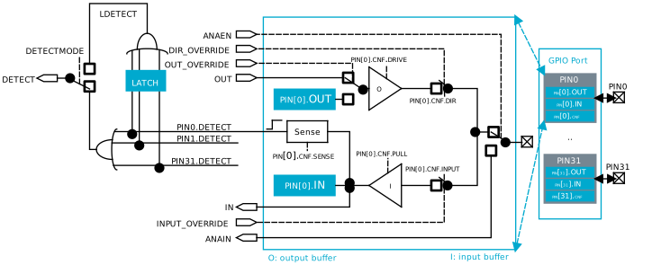
The following figure illustrates the GPIO port containing 32
individual pins, where PIN0 is illustrated in more detail as a reference. All
signals on the left side in the illustration are used by other peripherals in the system and
therefore not directly available to the CPU.
Pin configuration
The GPIO port peripheral implements up to 32 pins, PIN[n] (n = 0..31),
that can be individually configured in the PIN_CNF[n] registers (n=0..31).
The following parameters can be enabled or configured in these registers:
- Direction
- Drive strength
- Pull-up and pull-down resistors
- Pin sensing
- Input buffer disconnect
- Analog input (for selected pins)
All write-capable registers are retained registers. See POWER — Power control for more information.
When not used as an input, disconnect the input buffer of the GPIO pin to save power. An input must be connected to get a valid value in the IN register and for the sense mechanism to have access to the pin.
Other peripherals in the system can connect to GPIO pins to override their output value, override their configuration, or read their analog or digital input value.
Selected pins also support analog input signals (ANAIN). The assignment of the analog pins can be found in Pin assignments.
GPIO drive strength is configured using the DRIVE0 and DRIVE1 fields of register PIN_CNF[n] (n=0..31) (Retained). Some pins may not support every drive configuration, see Pin assignments for more information.
When a pin is configured as digital input, it is important to minimize increased current consumption when the input voltage is between VIL and VIH. It is a good practice to ensure that the external circuitry does not drive the pin to levels between VIL and VIH for a long period of time.
For more information on pin assignment and the corresponding effect of read and write operations of GPIO registers, see Peripheral and subsystem assignment.
Pin sense mechanism
Pin sensitivity can be individually configured through the SENSE field in the PIN_CNF[n] register to detect a high level or a low level on their input. When the correct level is detected, the sense mechanism will set the DETECT signal high. Each pin has a separate DETECT signal.
The default behavior for the DETECT signal is defined by the register DETECTMODE. By default, the DETECT signals from all pins in the GPIO port are combined into one common DETECT signal that is routed throughout the system, and can be utilized by other peripherals. This mechanism is functional in both System ON and System OFF modes.
Pins must be in a level that cannot trigger the sense mechanism before enabling it. When the sense mechanism is enabled, the DETECT signal will immediately go high if the SENSE condition configured in the PIN_CNF registers is met. This will trigger a PORT event if the DETECT signal was low before enabling the sense mechanism.
The DETECT signal is used by the power and clock management system to exit from System OFF mode, and by the GPIOTE peripheral to allow pins to generate events and interrupts.
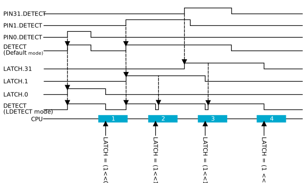
When a pin's PINx.DETECT signal goes high, a flag will be set in the register LATCH. For example, when the PIN0.DETECT signal goes high, bit 0 in the register LATCH will be set to 1. If the CPU performs a clear operation on a bit in the register LATCH when the associated PINx.DETECT signal is high, the bit in the register LATCH will not be cleared. The register LATCH will only be cleared if the CPU explicitly clears it by writing a 1 to the bit to be cleared. This means the register LATCH will not be affected by a PINx.DETECT signal being set low.
The LDETECT signal will be set high when one or more bits in the register LATCH 1. The LDETECT signal will be set low when all bits in the register LATCH are successfully cleared to 0.
If one or more bits in the register LATCH are 1 after the CPU has performed a clear operation, a rising edge will be generated on the LDETECT signal. This is illustrated in DETECT signal behavior.
LDETECT is enabled using the DETECTMODE register. See GPIO port and the GPIO pin details.
The following figure illustrates the DETECT signal behavior for these two alternatives.
Port capabilities
The device power domains have their own GPIO ports with different capabilities.
The following is a list of all GPIO ports (P[n]) in the system.
- P0 low-power domain – These I/O pins can wake the system up from System OFF or System ON sleep, and can be accessed by all peripherals in the low-power domain.
- P1 peripheral domain – These I/O pins can wake the system up from System OFF or System ON sleep, and can be accessed by all peripherals in the peripheral domain.
Peripherals cannot mix pins from different ports. All pins must be on the same port.
The following table lists the port special functions and characteristics.
| Port | Wakeup source | Extra high drive strength (E0E1) | Pin sense/detect | GPIOTE | Maximum speed [MHz] |
|---|---|---|---|---|---|
| P0 | Yes | No | Yes | Yes | 8 |
| P1 | Yes | No | Yes | Yes | 8 |
Please note that certain peripherals can operate the GPIOs at higher frequencies than those specified in the table above. In addition to the capabilities of the port, some specific pins have additional functions. These are listed in Pin assignments.
Peripheral and subsystem assignment
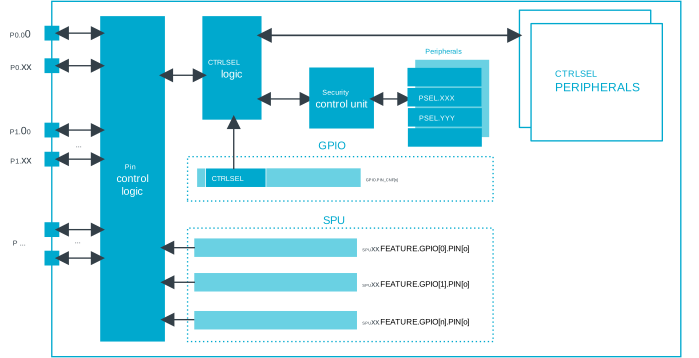
System GPIO pins can be allocated to peripherals with dedicated pins or subsystems such as trace and debug.
The pins of the system are listed in Pin assignments.
- GPIO or peripheral with PSEL registers
- Peripheral with dedicated pins (VPR and GRTC)
- Trace and debug (TND) subsystem
By default, all pins are assigned to GPIO or peripherals with PSEL registers. This is the default value of the CTRLSEL value in register PIN_CNF[n] (n=0..31) (Retained).
To allocate a pin to a peripheral or subsystem with dedicated pins, such as GRTC or TND, change the CTRLSEL value in register PIN_CNF[n] (n=0..31) (Retained) for that pin. This will connect the pin to the subsystem or peripheral.
Only the peripheral or subsystem where the pin was allocated can observe and control that pin's state. Reading a pin that is not allocated to the current subsystem will return zero, and writes will be ignored. If a pin is allocated to a subsystem that cannot access it, the pin stays under control of the GPIO peripheral.
When CTRLSEL is used to allocate a peripheral or subsystem, reading the GPIO peripheral registers will not reveal the state of the pins.
Clock pins
The device has dedicated clock pins. Some peripherals, such as SPI, TWI, and TRACE, have clock signals.
The dedicated clock pins are optimized to ensure correct timing between the clock and data signals for these peripherals. All peripherals that have clock signals must use these pins. See Pin assignments for the full list.
The data signal associated with the peripheral must use pins close to the clock pin. This ensures that the internal paths from the peripheral to the pin have the same delay, so that the data and clock signals reach the pins at the same time.
For high-speed signals, the printed circuit board (PCB) layout must use short PCB traces of identical length. This reduces delays and ensures the same delay on the clock and data path.
Weak pull-ups
A subset of the GPIO pins support weak pull-ups.
When enabled, the weak pull-ups are enabled for the complete set of GPIO pins connected to the weak pull-up module. Unlike GPIO, there is no per-pin configuration. Once enabled, the weak pull-up is applied to all GPIO pins that have weak pull-ups.
The set of pins that are connected to the weak pull-up module can be found in Pin assignments.
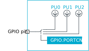
The pull-up is enabled on the full set of pins using PORTCNF.WEAKPU.
Reset behavior
- Retain their current configuration (e.g., outputs remain outputs, inputs remain inputs)
- Switch to high impedance, which is the default state upon device startup
Once nRESET is deasserted (rising edge), all GPIOs transition to the high impedance state until device firmware configures them.
When GPIO pins are in a high-impedance state for a prolonged period, external circuits that depend on a clearly defined logic level (either high or low) might require the use of external pull-up or pull-down resistors to ensure reliable operation. However, in most cases this is not required, as the duration of the high-impedance state during the reset cycle is typically very short.
Registers
Instances
| Instance | Domain | Base address | Description |
|---|---|---|---|
| P1 | GLOBAL | 0x400D8200 | General purpose input and output, port P1 |
| P0 | GLOBAL | 0x4010A000 | General purpose input and output, port P0 |
Configuration
| Instance | Domain | Configuration |
|---|---|---|
| P1 | GLOBAL | I/O pins on this port have pin sense mechanism This port has weak pull-ups on selected GPIO pins. P1 has 32 pins, P1.00 through P1.31. |
| P0 | GLOBAL | I/O pins on this port have pin sense mechanism P0 has 5 pins, P0.00 through P0.04. |
Register overview
| Register | Offset | Description |
|---|---|---|
| OUT | 0x000 | Write GPIO port This register is retained. |
| OUTSET | 0x004 | Set individual bits in GPIO port |
| OUTCLR | 0x008 | Clear individual bits in GPIO port |
| IN | 0x00C | Read GPIO port |
| DIR | 0x010 | Direction of GPIO pins This register is retained. |
| DIRSET | 0x014 | DIR set register |
| DIRCLR | 0x018 | DIR clear register |
| LATCH | 0x020 | Latch register indicating what GPIO pins that have met the criteria set in the PIN_CNF[n].SENSE registers This register is retained. |
| DETECTMODE | 0x024 | Select between default DETECT signal behavior and LDETECT mode This register is retained. |
| PORTCNF.WEAKPU | 0x30 | Control global weak pull-ups on the selected set of GPIO pins |
| PIN_CNF[n] | 0x080 | Pin n configuration of GPIO pin This register is retained. |
OUT (Retained)
Address offset: 0x000
Write GPIO port
This register is retained.
| Bit number | 31 | 30 | 29 | 28 | 27 | 26 | 25 | 24 | 23 | 22 | 21 | 20 | 19 | 18 | 17 | 16 | 15 | 14 | 13 | 12 | 11 | 10 | 9 | 8 | 7 | 6 | 5 | 4 | 3 | 2 | 1 | 0 | |||
|---|---|---|---|---|---|---|---|---|---|---|---|---|---|---|---|---|---|---|---|---|---|---|---|---|---|---|---|---|---|---|---|---|---|---|---|
| ID | f | e | d | c | b | a | Z | Y | X | W | V | U | T | S | R | Q | P | O | N | M | L | K | J | I | H | G | F | E | D | C | B | A | |||
| Reset 0x00000000 | 0 | 0 | 0 | 0 | 0 | 0 | 0 | 0 | 0 | 0 | 0 | 0 | 0 | 0 | 0 | 0 | 0 | 0 | 0 | 0 | 0 | 0 | 0 | 0 | 0 | 0 | 0 | 0 | 0 | 0 | 0 | 0 | |||
| ID | R/W | Field | Value ID | Value | Description | ||||||||||||||||||||||||||||||
| A-f | RW | PIN[i] (i=0..31) | Pin i | ||||||||||||||||||||||||||||||||
Low | 0 | Pin driver is low | |||||||||||||||||||||||||||||||||
High | 1 | Pin driver is high | |||||||||||||||||||||||||||||||||
OUTSET
Address offset: 0x004
Set individual bits in GPIO port
| Bit number | 31 | 30 | 29 | 28 | 27 | 26 | 25 | 24 | 23 | 22 | 21 | 20 | 19 | 18 | 17 | 16 | 15 | 14 | 13 | 12 | 11 | 10 | 9 | 8 | 7 | 6 | 5 | 4 | 3 | 2 | 1 | 0 | |||
|---|---|---|---|---|---|---|---|---|---|---|---|---|---|---|---|---|---|---|---|---|---|---|---|---|---|---|---|---|---|---|---|---|---|---|---|
| ID | f | e | d | c | b | a | Z | Y | X | W | V | U | T | S | R | Q | P | O | N | M | L | K | J | I | H | G | F | E | D | C | B | A | |||
| Reset 0x00000000 | 0 | 0 | 0 | 0 | 0 | 0 | 0 | 0 | 0 | 0 | 0 | 0 | 0 | 0 | 0 | 0 | 0 | 0 | 0 | 0 | 0 | 0 | 0 | 0 | 0 | 0 | 0 | 0 | 0 | 0 | 0 | 0 | |||
| ID | R/W | Field | Value ID | Value | Description | ||||||||||||||||||||||||||||||
| A-f | RW | PIN[i] (i=0..31) | Pin i | ||||||||||||||||||||||||||||||||
Low | 0 | Read: pin driver is low | |||||||||||||||||||||||||||||||||
High | 1 | Read: pin driver is high | |||||||||||||||||||||||||||||||||
Set | 1 | Write: writing a '1' sets the pin high; writing a '0' has no effect | |||||||||||||||||||||||||||||||||
OUTCLR
Address offset: 0x008
Clear individual bits in GPIO port
| Bit number | 31 | 30 | 29 | 28 | 27 | 26 | 25 | 24 | 23 | 22 | 21 | 20 | 19 | 18 | 17 | 16 | 15 | 14 | 13 | 12 | 11 | 10 | 9 | 8 | 7 | 6 | 5 | 4 | 3 | 2 | 1 | 0 | |||
|---|---|---|---|---|---|---|---|---|---|---|---|---|---|---|---|---|---|---|---|---|---|---|---|---|---|---|---|---|---|---|---|---|---|---|---|
| ID | f | e | d | c | b | a | Z | Y | X | W | V | U | T | S | R | Q | P | O | N | M | L | K | J | I | H | G | F | E | D | C | B | A | |||
| Reset 0x00000000 | 0 | 0 | 0 | 0 | 0 | 0 | 0 | 0 | 0 | 0 | 0 | 0 | 0 | 0 | 0 | 0 | 0 | 0 | 0 | 0 | 0 | 0 | 0 | 0 | 0 | 0 | 0 | 0 | 0 | 0 | 0 | 0 | |||
| ID | R/W | Field | Value ID | Value | Description | ||||||||||||||||||||||||||||||
| A-f | RW | PIN[i] (i=0..31) | Pin i | ||||||||||||||||||||||||||||||||
Low | 0 | Read: pin driver is low | |||||||||||||||||||||||||||||||||
High | 1 | Read: pin driver is high | |||||||||||||||||||||||||||||||||
Clear | 1 | Write: writing a '1' sets the pin low; writing a '0' has no effect | |||||||||||||||||||||||||||||||||
IN
Address offset: 0x00C
Read GPIO port
| Bit number | 31 | 30 | 29 | 28 | 27 | 26 | 25 | 24 | 23 | 22 | 21 | 20 | 19 | 18 | 17 | 16 | 15 | 14 | 13 | 12 | 11 | 10 | 9 | 8 | 7 | 6 | 5 | 4 | 3 | 2 | 1 | 0 | |||
|---|---|---|---|---|---|---|---|---|---|---|---|---|---|---|---|---|---|---|---|---|---|---|---|---|---|---|---|---|---|---|---|---|---|---|---|
| ID | f | e | d | c | b | a | Z | Y | X | W | V | U | T | S | R | Q | P | O | N | M | L | K | J | I | H | G | F | E | D | C | B | A | |||
| Reset 0x00000000 | 0 | 0 | 0 | 0 | 0 | 0 | 0 | 0 | 0 | 0 | 0 | 0 | 0 | 0 | 0 | 0 | 0 | 0 | 0 | 0 | 0 | 0 | 0 | 0 | 0 | 0 | 0 | 0 | 0 | 0 | 0 | 0 | |||
| ID | R/W | Field | Value ID | Value | Description | ||||||||||||||||||||||||||||||
| A-f | R | PIN[i] (i=0..31) | Pin i | ||||||||||||||||||||||||||||||||
Low | 0 | Pin input is low | |||||||||||||||||||||||||||||||||
High | 1 | Pin input is high | |||||||||||||||||||||||||||||||||
DIR (Retained)
Address offset: 0x010
Direction of GPIO pins
This register is retained.
| Bit number | 31 | 30 | 29 | 28 | 27 | 26 | 25 | 24 | 23 | 22 | 21 | 20 | 19 | 18 | 17 | 16 | 15 | 14 | 13 | 12 | 11 | 10 | 9 | 8 | 7 | 6 | 5 | 4 | 3 | 2 | 1 | 0 | |||
|---|---|---|---|---|---|---|---|---|---|---|---|---|---|---|---|---|---|---|---|---|---|---|---|---|---|---|---|---|---|---|---|---|---|---|---|
| ID | f | e | d | c | b | a | Z | Y | X | W | V | U | T | S | R | Q | P | O | N | M | L | K | J | I | H | G | F | E | D | C | B | A | |||
| Reset 0x00000000 | 0 | 0 | 0 | 0 | 0 | 0 | 0 | 0 | 0 | 0 | 0 | 0 | 0 | 0 | 0 | 0 | 0 | 0 | 0 | 0 | 0 | 0 | 0 | 0 | 0 | 0 | 0 | 0 | 0 | 0 | 0 | 0 | |||
| ID | R/W | Field | Value ID | Value | Description | ||||||||||||||||||||||||||||||
| A-f | RW | PIN[i] (i=0..31) | Pin i | ||||||||||||||||||||||||||||||||
Input | 0 | Pin set as input | |||||||||||||||||||||||||||||||||
Output | 1 | Pin set as output | |||||||||||||||||||||||||||||||||
DIRSET
Address offset: 0x014
DIR set register
| Bit number | 31 | 30 | 29 | 28 | 27 | 26 | 25 | 24 | 23 | 22 | 21 | 20 | 19 | 18 | 17 | 16 | 15 | 14 | 13 | 12 | 11 | 10 | 9 | 8 | 7 | 6 | 5 | 4 | 3 | 2 | 1 | 0 | |||
|---|---|---|---|---|---|---|---|---|---|---|---|---|---|---|---|---|---|---|---|---|---|---|---|---|---|---|---|---|---|---|---|---|---|---|---|
| ID | f | e | d | c | b | a | Z | Y | X | W | V | U | T | S | R | Q | P | O | N | M | L | K | J | I | H | G | F | E | D | C | B | A | |||
| Reset 0x00000000 | 0 | 0 | 0 | 0 | 0 | 0 | 0 | 0 | 0 | 0 | 0 | 0 | 0 | 0 | 0 | 0 | 0 | 0 | 0 | 0 | 0 | 0 | 0 | 0 | 0 | 0 | 0 | 0 | 0 | 0 | 0 | 0 | |||
| ID | R/W | Field | Value ID | Value | Description | ||||||||||||||||||||||||||||||
| A-f | RW | PIN[i] (i=0..31) | Set as output pin i | ||||||||||||||||||||||||||||||||
Input | 0 | Read: pin set as input | |||||||||||||||||||||||||||||||||
Output | 1 | Read: pin set as output | |||||||||||||||||||||||||||||||||
Set | 1 | Write: writing a '1' sets pin to output; writing a '0' has no effect | |||||||||||||||||||||||||||||||||
DIRCLR
Address offset: 0x018
DIR clear register
| Bit number | 31 | 30 | 29 | 28 | 27 | 26 | 25 | 24 | 23 | 22 | 21 | 20 | 19 | 18 | 17 | 16 | 15 | 14 | 13 | 12 | 11 | 10 | 9 | 8 | 7 | 6 | 5 | 4 | 3 | 2 | 1 | 0 | |||
|---|---|---|---|---|---|---|---|---|---|---|---|---|---|---|---|---|---|---|---|---|---|---|---|---|---|---|---|---|---|---|---|---|---|---|---|
| ID | f | e | d | c | b | a | Z | Y | X | W | V | U | T | S | R | Q | P | O | N | M | L | K | J | I | H | G | F | E | D | C | B | A | |||
| Reset 0x00000000 | 0 | 0 | 0 | 0 | 0 | 0 | 0 | 0 | 0 | 0 | 0 | 0 | 0 | 0 | 0 | 0 | 0 | 0 | 0 | 0 | 0 | 0 | 0 | 0 | 0 | 0 | 0 | 0 | 0 | 0 | 0 | 0 | |||
| ID | R/W | Field | Value ID | Value | Description | ||||||||||||||||||||||||||||||
| A-f | RW | PIN[i] (i=0..31) | Set as input pin i | ||||||||||||||||||||||||||||||||
Input | 0 | Read: pin set as input | |||||||||||||||||||||||||||||||||
Output | 1 | Read: pin set as output | |||||||||||||||||||||||||||||||||
Clear | 1 | Write: writing a '1' sets pin to input; writing a '0' has no effect | |||||||||||||||||||||||||||||||||
LATCH (Retained)
Address offset: 0x020
Latch register indicating what GPIO pins that have met the criteria set in the PIN_CNF[n].SENSE registers
This register is retained.
| Bit number | 31 | 30 | 29 | 28 | 27 | 26 | 25 | 24 | 23 | 22 | 21 | 20 | 19 | 18 | 17 | 16 | 15 | 14 | 13 | 12 | 11 | 10 | 9 | 8 | 7 | 6 | 5 | 4 | 3 | 2 | 1 | 0 | |||
|---|---|---|---|---|---|---|---|---|---|---|---|---|---|---|---|---|---|---|---|---|---|---|---|---|---|---|---|---|---|---|---|---|---|---|---|
| ID | f | e | d | c | b | a | Z | Y | X | W | V | U | T | S | R | Q | P | O | N | M | L | K | J | I | H | G | F | E | D | C | B | A | |||
| Reset 0x00000000 | 0 | 0 | 0 | 0 | 0 | 0 | 0 | 0 | 0 | 0 | 0 | 0 | 0 | 0 | 0 | 0 | 0 | 0 | 0 | 0 | 0 | 0 | 0 | 0 | 0 | 0 | 0 | 0 | 0 | 0 | 0 | 0 | |||
| ID | R/W | Field | Value ID | Value | Description | ||||||||||||||||||||||||||||||
| A-f | RW | PIN[i] (i=0..31) | Status on whether PINi has met criteria set in PIN_CNF[i].SENSE register. Write '1' to clear. | ||||||||||||||||||||||||||||||||
NotLatched | 0 | Criteria has not been met | |||||||||||||||||||||||||||||||||
Latched | 1 | Criteria has been met | |||||||||||||||||||||||||||||||||
DETECTMODE (Retained)
Address offset: 0x024
Select between default DETECT signal behavior and LDETECT mode
This register is retained.
| Bit number | 31 | 30 | 29 | 28 | 27 | 26 | 25 | 24 | 23 | 22 | 21 | 20 | 19 | 18 | 17 | 16 | 15 | 14 | 13 | 12 | 11 | 10 | 9 | 8 | 7 | 6 | 5 | 4 | 3 | 2 | 1 | 0 | |||
|---|---|---|---|---|---|---|---|---|---|---|---|---|---|---|---|---|---|---|---|---|---|---|---|---|---|---|---|---|---|---|---|---|---|---|---|
| ID | A | ||||||||||||||||||||||||||||||||||
| Reset 0x00000000 | 0 | 0 | 0 | 0 | 0 | 0 | 0 | 0 | 0 | 0 | 0 | 0 | 0 | 0 | 0 | 0 | 0 | 0 | 0 | 0 | 0 | 0 | 0 | 0 | 0 | 0 | 0 | 0 | 0 | 0 | 0 | 0 | |||
| ID | R/W | Field | Value ID | Value | Description | ||||||||||||||||||||||||||||||
| A | RW | DETECTMODE | Select between default DETECT signal behavior and LDETECT mode | ||||||||||||||||||||||||||||||||
Default | 0 | DETECT directly connected to PIN DETECT signals | |||||||||||||||||||||||||||||||||
LDETECT | 1 | Use the latched LDETECT behavior | |||||||||||||||||||||||||||||||||
PORTCNF.WEAKPU
Address offset: 0x30
Control global weak pull-ups on the selected set of GPIO pins
| Bit number | 31 | 30 | 29 | 28 | 27 | 26 | 25 | 24 | 23 | 22 | 21 | 20 | 19 | 18 | 17 | 16 | 15 | 14 | 13 | 12 | 11 | 10 | 9 | 8 | 7 | 6 | 5 | 4 | 3 | 2 | 1 | 0 | |||
|---|---|---|---|---|---|---|---|---|---|---|---|---|---|---|---|---|---|---|---|---|---|---|---|---|---|---|---|---|---|---|---|---|---|---|---|
| ID | A | A | |||||||||||||||||||||||||||||||||
| Reset 0x00000000 | 0 | 0 | 0 | 0 | 0 | 0 | 0 | 0 | 0 | 0 | 0 | 0 | 0 | 0 | 0 | 0 | 0 | 0 | 0 | 0 | 0 | 0 | 0 | 0 | 0 | 0 | 0 | 0 | 0 | 0 | 0 | 0 | |||
| ID | R/W | Field | Value ID | Value | Description | ||||||||||||||||||||||||||||||
| A | RW | PULLUP | Control pull-up. | ||||||||||||||||||||||||||||||||
Disabled | 0 | Pull-up is disabled. | |||||||||||||||||||||||||||||||||
PU0 | 1 | Enable pull-up 0. | |||||||||||||||||||||||||||||||||
PU1 | 2 | Enable pull-up 1. | |||||||||||||||||||||||||||||||||
PU2 | 3 | Enable pull-up 2. | |||||||||||||||||||||||||||||||||
PIN_CNF[n]
Address offset: 0x080 + (n × 0x4)
Pin n configuration of GPIO pin
This register is retained.
| Bit number | 31 | 30 | 29 | 28 | 27 | 26 | 25 | 24 | 23 | 22 | 21 | 20 | 19 | 18 | 17 | 16 | 15 | 14 | 13 | 12 | 11 | 10 | 9 | 8 | 7 | 6 | 5 | 4 | 3 | 2 | 1 | 0 | |||
|---|---|---|---|---|---|---|---|---|---|---|---|---|---|---|---|---|---|---|---|---|---|---|---|---|---|---|---|---|---|---|---|---|---|---|---|
| ID | G | G | G | F | F | E | E | D | D | C | C | B | A | ||||||||||||||||||||||
| Reset 0x00000002 | 0 | 0 | 0 | 0 | 0 | 0 | 0 | 0 | 0 | 0 | 0 | 0 | 0 | 0 | 0 | 0 | 0 | 0 | 0 | 0 | 0 | 0 | 0 | 0 | 0 | 0 | 0 | 0 | 0 | 0 | 1 | 0 | |||
| ID | R/W | Field | Value ID | Value | Description | ||||||||||||||||||||||||||||||
| A | RW | DIR | Pin direction. Same physical register as DIR register | ||||||||||||||||||||||||||||||||
Input | 0 | Configure pin as an input pin | |||||||||||||||||||||||||||||||||
Output | 1 | Configure pin as an output pin | |||||||||||||||||||||||||||||||||
| B | RW | INPUT | Connect or disconnect input buffer | ||||||||||||||||||||||||||||||||
Connect | 0 | Connect input buffer | |||||||||||||||||||||||||||||||||
Disconnect | 1 | Disconnect input buffer | |||||||||||||||||||||||||||||||||
| C | RW | PULL | Pull configuration | ||||||||||||||||||||||||||||||||
Disabled | 0 | No pull | |||||||||||||||||||||||||||||||||
Pulldown | 1 | Pull down on pin | |||||||||||||||||||||||||||||||||
Pullup | 3 | Pull up on pin | |||||||||||||||||||||||||||||||||
| D | RW | DRIVE0 | Drive configuration for '0' | ||||||||||||||||||||||||||||||||
S0 | 0 | Standard '0' | |||||||||||||||||||||||||||||||||
H0 | 1 | High drive '0' | |||||||||||||||||||||||||||||||||
D0 | 2 | Disconnect '0'(normally used for wired-or connections) | |||||||||||||||||||||||||||||||||
E0 | 3 | Extra high drive '0' Note: The DRIVE1 must be E1 as well to work properly. | |||||||||||||||||||||||||||||||||
| E | RW | DRIVE1 | Drive configuration for '1' | ||||||||||||||||||||||||||||||||
S1 | 0 | Standard '1' | |||||||||||||||||||||||||||||||||
H1 | 1 | High drive '1' | |||||||||||||||||||||||||||||||||
D1 | 2 | Disconnect '1'(normally used for wired-or connections) | |||||||||||||||||||||||||||||||||
E1 | 3 | Extra high drive '1' Note: The DRIVE0 must be E0 as well to work properly. | |||||||||||||||||||||||||||||||||
| F | RW | SENSE | Pin sensing mechanism | ||||||||||||||||||||||||||||||||
Disabled | 0 | Disabled | |||||||||||||||||||||||||||||||||
High | 2 | Sense for high level | |||||||||||||||||||||||||||||||||
Low | 3 | Sense for low level | |||||||||||||||||||||||||||||||||
| G | RW | CTRLSEL | Select which module has direct control over this pin | ||||||||||||||||||||||||||||||||
GPIO | 0x0 | GPIO or peripherals with PSEL registers | |||||||||||||||||||||||||||||||||
VPR | 0x1 | VPR processor | |||||||||||||||||||||||||||||||||
GRTC | 0x4 | GRTC peripheral | |||||||||||||||||||||||||||||||||