GRTC — Global real-time counter
The global real-time counter peripheral (GRTC) is an ultra-low power shared system timer. GRTC implements a high-resolution system timer that is available in all power modes, including System OFF.
The system timer has a 1 μs resolution and is 52 bits wide. This provides a run time of 142 years after initial power-on until the counter wraps around. It uses the 16 MHz clock when the high-speed clock is active, but automatically switches to 32.768 kHz in the other power modes. It will continue to be updated in all power modes. Due to the combination of clock sources, it has a 1 μs resolution and an accuracy equal to the 32.768 kHz clock.
The main features of GRTC are the following:
- System timer – SYSCOUNTER
- 1 µs resolution
- Multiple compare/capture channels on SYSCOUNTER
- PPI connection
- Periodic interval generation for one compare event
- Wake up from System OFF mode
- Pulse Width Modulation (PWM)
- Single channel PWM
- Operates in System OFF mode
- Clock output on pin
- LFCLK
- Configurable divided fast clock output
The system timer is a high resolution timer which can be accessed by all processors in the system. It allows the same system counter to be shared among all users. GRTC can operate in System OFF mode.
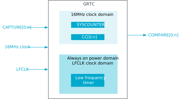
All GRTC registers are reset during wakeup from System OFF mode. However, the SYSCOUNTER[m].SYSCOUNTERL and SYSCOUNTER[m].SYSCOUNTERH registers are restored automatically on wakeup from System OFF mode and after soft reset.
GRTC clock sources
The low frequency timer in GRTC will run off the LFCLK.
When the low frequency timer is started, the GRTC peripheral will automatically request the LFCLK source if the LFCLK is not already running.
The GRTC low frequency timer clock source can be selected using register CLKCFG.CLKSEL. The clock source cannot be changed after GRTC is started.
The clock source selection at GRTC is retained internally during System OFF mode, even though the CLKCFG.CLKSEL is reset on wakeup.
The SYSCOUNTER runs off the fast clock (16MHz clock), but uses only LFCLK while SYSCOUNTER is in sleep state.
See CLOCK for more information about clock sources.
SYSCOUNTER
The internal counter at SYSCOUNTER increments every 1 µs.
SYSCOUNTER is a 52-bit counter and is enabled using MODE.SYSCOUNTEREN register. The internal low frequency timer must be started for the proper operation of the SYSCOUNTER while SYSCOUNTER goes into sleep mode. It can be started by the TASKS_START task and can be stopped by the TASKS_STOP task when SYSCOUNTER is no more in use.
The current value of SYSCOUNTER can be read using corresponding SYSCOUNTER[m].SYSCOUNTERL and SYSCOUNTER[m].SYSCOUNTERH. But, the SYSCOUNTER[m].SYSCOUNTERL must be read before corresponding SYSCOUNTER[m].SYSCOUNTERH. The SYSCOUNTER[m].SYSCOUNTERH.OVERFLOW indicates if the SYSCOUNTER[m].SYSCOUNTERL is overflown after reading it.
      uint32_t syscounterl_value, syscounterh_value, syscounterh;
      uint64_t syscounter;

      do
      {
        syscounterl_value = GRTC.SYSCOUNTER[m].SYSCOUNTERL;
        syscounterh = GRTC.SYSCOUNTER[m].SYSCOUNTERH;

        syscounterh_value = ((syscounterh & GRTC_SYSCOUNTER_SYSCOUNTERH_VALUE_Msk) >> GRTC_SYSCOUNTER_SYSCOUNTERH_VALUE_Pos);

        if (((syscounterh & GRTC_SYSCOUNTER_SYSCOUNTERH_OVERFLOW_Msk) >> GRTC_SYSCOUNTER_SYSCOUNTERH_OVERFLOW_Pos) == GRTC_SYSCOUNTER_SYSCOUNTERH_OVERFLOW_Overflow)
        {
          syscounterh = syscounterh_value - 1;
        }

      } while (((syscounterh & GRTC_SYSCOUNTER_SYSCOUNTERH_BUSY_Msk) >> GRTC_SYSCOUNTER_SYSCOUNTERH_BUSY_Pos) != GRTC_SYSCOUNTER_SYSCOUNTERH_BUSY_Ready);

      syscounter = (syscounterh_value << 32) + syscounterl_value;
Compare and Capture (CC)
The CC[n] is a group of registers interfacing the compare and capture channels of SYSCOUNTER, where n is the number of compare and capture channels specified in the GRTC instance configuration table below. Each CC[n] has an associated TASKS_CAPTURE[n] task and EVENTS_COMPARE[n] event. Each channel compare functionality can be enabled/disabled with CC[n].CCEN.ACTIVE, and its current active state read from this same register.
The EVENTS_COMPARE[n] event can be generated by writing the compare values to the corresponding CC[n].CCL and CC[n].CCH registers. When a channel compare functionality is enabled and SYSCOUNTER is equal or greater than that CC value EVENTS_COMPARE[n] will be generated. Writes to CC[n].CCL disable the corresponding compare channel and writes to CC[n].CCH enable it. So CC[n].CCL must be written first.
Each channel compare functionality, except for the first channel when operating in periodic mode, operates in one-shot mode. When operating in one-shot mode, CC[n].CCEN.ACTIVE is cleared automatically following a compare event.
Moreover, a compare channel is automatically disabled when triggering TASKS_CAPTURE[n].
The EVENTS_COMPARE[n] event is generated immediately if the configured compare value at CC[n] is less than the current SYSCOUNTER value. The status CC[n].CCEN.PASTCC indicates this condition.
Every time the TASKS_CAPTURE[n] task is triggered, the current SYSCOUNTER is copied into the corresponding CC[n].CCL and CC[n].CCH registers. The CC[n].CCL and CC[n].CCH registers can be read in any order. The TASKS_CAPTURE[n] task will not generate EVENTS_COMPARE[n] event.
The TASKS_CAPTURE[n] tasks and EVENTS_COMPARE[n] events can be connected with the PPI. However, the TASKS_CAPTURE[n] is functional only when the SYSCOUNTER is in active state. The GRTC can be forced into active state by setting any SYSCOUNTER[n].ACTIVE register.
The compare value for CC[n] can also be updated by adding a fixed value provided at CC[n].CCADD.VALUE. Based on the CC[n].CCADD.REFERENCE configuration, either the current CC value or the current SYSCOUNTER value is added to the CC[n].CCADD.VALUE to configure the new compare value. If the CC[n] overflows after writing to CC[n].CCADD.VALUE, then EVENTS_COMPARE[n] is generated immediately. Writing to CC[n].CCADD enables the corresponding compare channel.
Writes to CC[n].CCADD are ignored when the SYSCOUNTER is in sleep state.
Periodic interval
In addition to one-shot mode, the CC[0] can produce periodic EVENTS_COMPARE[0] event without any software interaction. The interval between these events can be programmed using INTERVAL register and non-zero interval enables this periodic interval feature. On every EVENTS_COMPARE[0] event, CC[0] becomes CC[0] + INTERVAL.
SYSCOUNTER sleep mode
- SYSCOUNTER is in active state
- SYSCOUNTER is in sleep state - This is the GRTC ultra-low power sleep mode
To save power, SYSCOUNTER automatically goes into sleep state when there is no activity.
Before SYSCOUNTER goes into sleep state, the GRTC configures the internal low frequency timer compare match based on the next expected SYSCOUNTER compare match using CC[n] configuration. An internal event on low frequency timer is generated when the compare match happens.
The internal counter at SYSCOUNTER is not ticking when SYSCOUNTER is in sleep state, the internal low frequency timer is configured as described above.
- Any of SYSCOUNTER[n].ACTIVE register is set to Active
- SYSCOUNTER counter value is read
- Any of the following registers are written:
- MODE
- CC[n]
- INTENn/INTENSETn/INTENCLRn/INTENPENDn
- Write to tasks TASKS_START, TASKS_STOP and TASKS_CLEAR
- When internal low frequency timer compare match happens
- Any CPU is not sleeping, if MODE.AUTOEN is set
On wake up to active state, SYSCOUNTER is updated based on the internal low frequency timer compare match. The status SYSCOUNTER[m].SYSCOUNTERH.BUSY indicates SYSCOUNTER is synchronized and valid after the SYSCOUNTER is woken up.
The status SYSCOUNTER[m].SYSCOUNTERH.LOADED indicates SYSCOUNTER is loaded after wake up, but not synchomized to the low frequency clock yet. This gives early indication of the SYSCOUNTER value, whcih may vary approximately one low frequency clcok cycle.
- SYSCOUNTER[m].SYSCOUNTERH.BUSY = 1 and SYSCOUNTER[m].SYSCOUNTERH.LOADED = 0 : SYSCCOUNTER is in sleep and SYSCOUNTER[m].SYSCOUNTER value is invalid
- SYSCOUNTER[m].SYSCOUNTERH.BUSY = 1 and SYSCOUNTER[m].SYSCOUNTERH.LOADED = 1 : SYSCCOUNTER is in woken up and SYSCOUNTER[m].SYSCOUNTER value is updated but not synchronized to low frequency clock yet
- SYSCOUNTER[m].SYSCOUNTERH.BUSY = 0 and SYSCOUNTER[m].SYSCOUNTERH.LOADED = 1 : SYSCOUNTER[m].SYSCOUNTER value is valid
Before handling next scheduled EVENTS_COMPARE[n] event, GRTC must wake up from the low power state. The WAKETIME register configures the number of LFCLK cycles that GRTC will wake up before the compare event. This duration allows the device sufficient time to power up, initialize, and activate the necessary clocks to accurately generate and handle events from the GRTC SYSCOUNTER. A longer system wake-up time requires a larger WAKETIME value to ensure reliable event processing. When the device is in System OFF, the WAKETIME must cover the system wakeup time from System OFF mode and in addition the required time the system uses to configure GRTC and enable the event.
All GRTC registers must be restored at wakeup from system OFF before the next scheduled COMPARE[n] event is generated. The TIMEOUT register must be configured to a value higher than WAKETIME (TIMEOUT > WAKETIME + guard_time). This makes sure that GRTC is not entering sleep again if the next event is nearer than TIMEOUT LFCLK cycles. The minimum guard time is 1 LFCLK cycle.
Recommendation on reading SYSCOUNTER
- Set the corresponding SYSCOUNTER[m].ACTIVE to Active
- Wait until the corresponding status SYSCOUNTER[m].SYSCOUNTERH.BUSY is cleared
- Read the corresponding SYSCOUNTER[m].SYSCOUNTERL/H values
- Clear the SYSCOUNTER[m].ACTIVE set above
Entering System OFF mode
- Set the SYSCOUNTER in active state, either
- Set MODE.AUTOEN
- Set corresponding SYSCOUNTER[m].ACTIVE to Active
- If GRTC is wakeup source, then set the corresponding CC[n] value to expected wakeup time
- Set WAKETIME for the boot latency
- Set the SYSCOUNTER in sleep state, by clearing the configuration set at step 1 above
- Wait for either of EVENTS_RTCOMPARESYNC or any EVENTS_COMPARE[n]
- If any EVENTS_COMPARE[n] triggered,
- Allow CPUs to wakeup on interrupts
- Do not enter System OFF mode
- Else,
- Enter System OFF by using the SYSTEMOFF register
- If any EVENTS_COMPARE[n] triggered,
Pulse Width Modulation (PWM)
The GRTC peripheral has a built-in PWM that can drive one output pin as an 8-bit non-inverted pulse-width modulated output.
The PWM is based on the internal low frequency timer of the GRTC and the PWM has a period of 256 LFCLK clock cycles, resulting frequency is 128Hz.
The PWM can be started by the TASKS_PWMSTART task and can be stopped by the TASKS_PWMSTOP task. The PWM starts/stops on next time when the lower 8 bits of internal low frequency timer becomes to zero. It takes up to 256 LFCLK clock cycles to take these tasks to go into effect.
The PWM compare value is configured using PWMCONFIG and the copied to the internal PWM compare register when the lower 8 bits of internal low frequency timer is 0.
The PWM output goes high when the the lower 8 bits of internal low frequency timer goes to zero and the PWM output goes low when the lower 8 bits of internal low frequency timer matches the PWM compare value. The EVENTS_PWMPERIODEND event is generated on the rising edge of the PWM output.
To optimize the GRTC power consumption, the EVENTS_PWMPERIODEND can be disabled using EVTEN/EVTENSET/EVTENCLR registers to prevent clock from being requested when those events are triggered.
The PWM is operating even while the device is in system OFF.
For the PWM output pin mapping, see Pin assignments. GRTC uses standard output drive strength for PWM output.
Clock output
The GRTC can be configured to output the clock on a pin.
- LFCLK (32 KHz clock) output
- Divided 16M Hz clock (fast clock) output
The clock outputs can be enabled or disabled using CLKOUT.
The 16 MHz clock is divided before it is output on a pin. The divisor can be configured in CLKCFG, where clock output is (fast clock) / (CLKCFG.CLKFASTDIV * 2). The CLKCFG.CLKFASTDIV should be changed only when CLKOUT.CLKOUTFAST is disabled.
The LFCLK clock is output also when the device is in System OFF mode.
For the clock output pin mapping, see Pin assignments. GRTC uses standard output drive strength for clock output.
Task priority
If the START task and the STOP task are triggered at the same time, meaning within the same period of LFCLK, the STOP task is prioritized.
If one or more of the CAPTURE tasks and the CLEAR task are triggered at the same time, that is, within the same period of LFCLP, the CAPTURE tasks are prioritized. This means that the CC registers will capture the counter value before the CLEAR tasks are triggered.
Registers
Instances
| Instance | Domain | Base address | Description |
|---|---|---|---|
| GRTC | GLOBAL | 0x400E2000 | Global RTC GRTC |
Configuration
| Instance | Domain | Configuration |
|---|---|---|
| GRTC | GLOBAL | Local CPUs connected to MODE.AUTO.EN.CpuActive : Application core Arm Cortex-M33. CLKSEL settings XO and LFLPRC must be used for lowest possible power consumption in sleep modes. Width of the RTCOUNTERH, RTCOMPAREH and RTCOMPARESYNCH registers : 0..14 Number of compare/capture registers : 0..11 Width of the TIMEOUT register : 0..15 Number of GRTC interrupts : 0..3 The PWM registers are available. The CLKOUT register is available. The CLKCFG.CLKSEL register is available. The CLKCFG.CLKSEL register supports LFLPRC. The CC[n].CCADD register has write access only. The ready status and events are available. SYSCOUNTER[n].SYSCOUNTERH.LOADED status is available CC[n].CCEN.PASTCC status is available 4 interrupts with interrupt remapping 12 capture compare channels implemented |
Register overview
| Register | Offset | Description |
|---|---|---|
| TASKS_CAPTURE[n] | 0x000 | Capture the counter value to CC[n] register |
| TASKS_START | 0x060 | Start the counter |
| TASKS_STOP | 0x064 | Stop the counter |
| TASKS_CLEAR | 0x068 | Clear the counter |
| TASKS_PWMSTART | 0x06C | Start the PWM |
| TASKS_PWMSTOP | 0x070 | Stop the PWM |
| SUBSCRIBE_CAPTURE[n] | 0x080 | Subscribe configuration for task CAPTURE[n] |
| EVENTS_COMPARE[n] | 0x100 | Compare event on CC[n] match |
| EVENTS_RTCOMPARESYNC | 0x164 | The GRTC low frequency timer is synchronized with the SYSCOUNTER |
| EVENTS_PWMPERIODEND | 0x16C | Event on end of each PWM period |
| EVENTS_PWMREADY | 0x174 | Event on STATUS.PWM.READY status changed to ready |
| EVENTS_CLKOUTREADY | 0x178 | Event on STATUS.CLKOUT.READY status changed to ready |
| PUBLISH_COMPARE[n] | 0x180 | Publish configuration for event COMPARE[n] |
| PUBLISH_PWMREADY | 0x1F4 | Publish configuration for event PWMREADY |
| PUBLISH_CLKOUTREADY | 0x1F8 | Publish configuration for event CLKOUTREADY |
| SHORTS | 0x200 | Shortcuts between local events and tasks |
| INTEN0 | 0x300 | Enable or disable interrupt |
| INTENSET0 | 0x304 | Enable interrupt |
| INTENCLR0 | 0x308 | Disable interrupt |
| INTPEND0 | 0x30C | Pending interrupts |
| INTEN1 | 0x310 | Enable or disable interrupt |
| INTENSET1 | 0x314 | Enable interrupt |
| INTENCLR1 | 0x318 | Disable interrupt |
| INTPEND1 | 0x31C | Pending interrupts |
| INTEN2 | 0x320 | Enable or disable interrupt |
| INTENSET2 | 0x324 | Enable interrupt |
| INTENCLR2 | 0x328 | Disable interrupt |
| INTPEND2 | 0x32C | Pending interrupts |
| INTEN3 | 0x330 | Enable or disable interrupt |
| INTENSET3 | 0x334 | Enable interrupt |
| INTENCLR3 | 0x338 | Disable interrupt |
| INTPEND3 | 0x33C | Pending interrupts |
| EVTEN | 0x400 | Enable or disable event routing |
| EVTENSET | 0x404 | Enable event routing |
| EVTENCLR | 0x408 | Disable event routing |
| MODE | 0x510 | Counter mode selection |
| CC[n].CCL | 0x520 | The lower 32-bits of Capture/Compare register CC[n] |
| CC[n].CCH | 0x524 | The higher 32-bits of Capture/Compare register CC[n] |
| CC[n].CCADD | 0x528 | Count to add to CC[n] when this register is written. |
| CC[n].CCEN | 0x52C | Configure Capture/Compare register CC[n] |
| TIMEOUT | 0x6A4 | Timeout after all CPUs gone into sleep state to stop the SYSCOUNTER |
| INTERVAL | 0x6A8 | Count to add to CC[0] when the event EVENTS_COMPARE[0] triggers. |
| WAKETIME | 0x6AC | GRTC wake up time. |
| STATUS.LFTIMER | 0x6B0 | Low frequency timer status. |
| STATUS.PWM | 0x6B4 | PWM status. |
| STATUS.CLKOUT | 0x6B8 | CLKOUT configuration status. |
| PWMCONFIG | 0x710 | PWM configuration. |
| CLKOUT | 0x714 | Configuration of clock output |
| CLKCFG | 0x718 | Clock Configuration |
| SYSCOUNTER[n].SYSCOUNTERL | 0x720 | The lower 32-bits of the SYSCOUNTER for index [n] |
| SYSCOUNTER[n].SYSCOUNTERH | 0x724 | The higher 20-bits of the SYSCOUNTER for index [n] |
| SYSCOUNTER[n].ACTIVE | 0x728 | Request to keep the SYSCOUNTER in the active state and prevent going to sleep for index [n] |
TASKS_CAPTURE[n]
Address offset: 0x000 + (n × 0x4)
Capture the counter value to CC[n] register
| Bit number | 31 | 30 | 29 | 28 | 27 | 26 | 25 | 24 | 23 | 22 | 21 | 20 | 19 | 18 | 17 | 16 | 15 | 14 | 13 | 12 | 11 | 10 | 9 | 8 | 7 | 6 | 5 | 4 | 3 | 2 | 1 | 0 | |||
|---|---|---|---|---|---|---|---|---|---|---|---|---|---|---|---|---|---|---|---|---|---|---|---|---|---|---|---|---|---|---|---|---|---|---|---|
| ID | A | ||||||||||||||||||||||||||||||||||
| Reset 0x00000000 | 0 | 0 | 0 | 0 | 0 | 0 | 0 | 0 | 0 | 0 | 0 | 0 | 0 | 0 | 0 | 0 | 0 | 0 | 0 | 0 | 0 | 0 | 0 | 0 | 0 | 0 | 0 | 0 | 0 | 0 | 0 | 0 | |||
| ID | R/W | Field | Value ID | Value | Description | ||||||||||||||||||||||||||||||
| A | W | TASKS_CAPTURE | Capture the counter value to CC[n] register | ||||||||||||||||||||||||||||||||
Trigger | 1 | Trigger task | |||||||||||||||||||||||||||||||||
TASKS_START
Address offset: 0x060
Start the counter
| Bit number | 31 | 30 | 29 | 28 | 27 | 26 | 25 | 24 | 23 | 22 | 21 | 20 | 19 | 18 | 17 | 16 | 15 | 14 | 13 | 12 | 11 | 10 | 9 | 8 | 7 | 6 | 5 | 4 | 3 | 2 | 1 | 0 | |||
|---|---|---|---|---|---|---|---|---|---|---|---|---|---|---|---|---|---|---|---|---|---|---|---|---|---|---|---|---|---|---|---|---|---|---|---|
| ID | A | ||||||||||||||||||||||||||||||||||
| Reset 0x00000000 | 0 | 0 | 0 | 0 | 0 | 0 | 0 | 0 | 0 | 0 | 0 | 0 | 0 | 0 | 0 | 0 | 0 | 0 | 0 | 0 | 0 | 0 | 0 | 0 | 0 | 0 | 0 | 0 | 0 | 0 | 0 | 0 | |||
| ID | R/W | Field | Value ID | Value | Description | ||||||||||||||||||||||||||||||
| A | W | TASKS_START | Start the counter | ||||||||||||||||||||||||||||||||
Trigger | 1 | Trigger task | |||||||||||||||||||||||||||||||||
TASKS_STOP
Address offset: 0x064
Stop the counter
| Bit number | 31 | 30 | 29 | 28 | 27 | 26 | 25 | 24 | 23 | 22 | 21 | 20 | 19 | 18 | 17 | 16 | 15 | 14 | 13 | 12 | 11 | 10 | 9 | 8 | 7 | 6 | 5 | 4 | 3 | 2 | 1 | 0 | |||
|---|---|---|---|---|---|---|---|---|---|---|---|---|---|---|---|---|---|---|---|---|---|---|---|---|---|---|---|---|---|---|---|---|---|---|---|
| ID | A | ||||||||||||||||||||||||||||||||||
| Reset 0x00000000 | 0 | 0 | 0 | 0 | 0 | 0 | 0 | 0 | 0 | 0 | 0 | 0 | 0 | 0 | 0 | 0 | 0 | 0 | 0 | 0 | 0 | 0 | 0 | 0 | 0 | 0 | 0 | 0 | 0 | 0 | 0 | 0 | |||
| ID | R/W | Field | Value ID | Value | Description | ||||||||||||||||||||||||||||||
| A | W | TASKS_STOP | Stop the counter | ||||||||||||||||||||||||||||||||
Trigger | 1 | Trigger task | |||||||||||||||||||||||||||||||||
TASKS_CLEAR
Address offset: 0x068
Clear the counter
| Bit number | 31 | 30 | 29 | 28 | 27 | 26 | 25 | 24 | 23 | 22 | 21 | 20 | 19 | 18 | 17 | 16 | 15 | 14 | 13 | 12 | 11 | 10 | 9 | 8 | 7 | 6 | 5 | 4 | 3 | 2 | 1 | 0 | |||
|---|---|---|---|---|---|---|---|---|---|---|---|---|---|---|---|---|---|---|---|---|---|---|---|---|---|---|---|---|---|---|---|---|---|---|---|
| ID | A | ||||||||||||||||||||||||||||||||||
| Reset 0x00000000 | 0 | 0 | 0 | 0 | 0 | 0 | 0 | 0 | 0 | 0 | 0 | 0 | 0 | 0 | 0 | 0 | 0 | 0 | 0 | 0 | 0 | 0 | 0 | 0 | 0 | 0 | 0 | 0 | 0 | 0 | 0 | 0 | |||
| ID | R/W | Field | Value ID | Value | Description | ||||||||||||||||||||||||||||||
| A | W | TASKS_CLEAR | Clear the counter | ||||||||||||||||||||||||||||||||
Trigger | 1 | Trigger task | |||||||||||||||||||||||||||||||||
TASKS_PWMSTART
Address offset: 0x06C
Start the PWM
| Bit number | 31 | 30 | 29 | 28 | 27 | 26 | 25 | 24 | 23 | 22 | 21 | 20 | 19 | 18 | 17 | 16 | 15 | 14 | 13 | 12 | 11 | 10 | 9 | 8 | 7 | 6 | 5 | 4 | 3 | 2 | 1 | 0 | |||
|---|---|---|---|---|---|---|---|---|---|---|---|---|---|---|---|---|---|---|---|---|---|---|---|---|---|---|---|---|---|---|---|---|---|---|---|
| ID | A | ||||||||||||||||||||||||||||||||||
| Reset 0x00000000 | 0 | 0 | 0 | 0 | 0 | 0 | 0 | 0 | 0 | 0 | 0 | 0 | 0 | 0 | 0 | 0 | 0 | 0 | 0 | 0 | 0 | 0 | 0 | 0 | 0 | 0 | 0 | 0 | 0 | 0 | 0 | 0 | |||
| ID | R/W | Field | Value ID | Value | Description | ||||||||||||||||||||||||||||||
| A | W | TASKS_PWMSTART | Start the PWM | ||||||||||||||||||||||||||||||||
Trigger | 1 | Trigger task | |||||||||||||||||||||||||||||||||
TASKS_PWMSTOP
Address offset: 0x070
Stop the PWM
| Bit number | 31 | 30 | 29 | 28 | 27 | 26 | 25 | 24 | 23 | 22 | 21 | 20 | 19 | 18 | 17 | 16 | 15 | 14 | 13 | 12 | 11 | 10 | 9 | 8 | 7 | 6 | 5 | 4 | 3 | 2 | 1 | 0 | |||
|---|---|---|---|---|---|---|---|---|---|---|---|---|---|---|---|---|---|---|---|---|---|---|---|---|---|---|---|---|---|---|---|---|---|---|---|
| ID | A | ||||||||||||||||||||||||||||||||||
| Reset 0x00000000 | 0 | 0 | 0 | 0 | 0 | 0 | 0 | 0 | 0 | 0 | 0 | 0 | 0 | 0 | 0 | 0 | 0 | 0 | 0 | 0 | 0 | 0 | 0 | 0 | 0 | 0 | 0 | 0 | 0 | 0 | 0 | 0 | |||
| ID | R/W | Field | Value ID | Value | Description | ||||||||||||||||||||||||||||||
| A | W | TASKS_PWMSTOP | Stop the PWM | ||||||||||||||||||||||||||||||||
Trigger | 1 | Trigger task | |||||||||||||||||||||||||||||||||
SUBSCRIBE_CAPTURE[n]
Address offset: 0x080 + (n × 0x4)
Subscribe configuration for task CAPTURE[n]
| Bit number | 31 | 30 | 29 | 28 | 27 | 26 | 25 | 24 | 23 | 22 | 21 | 20 | 19 | 18 | 17 | 16 | 15 | 14 | 13 | 12 | 11 | 10 | 9 | 8 | 7 | 6 | 5 | 4 | 3 | 2 | 1 | 0 | |||
|---|---|---|---|---|---|---|---|---|---|---|---|---|---|---|---|---|---|---|---|---|---|---|---|---|---|---|---|---|---|---|---|---|---|---|---|
| ID | B | A | A | A | A | A | A | A | A | ||||||||||||||||||||||||||
| Reset 0x00000000 | 0 | 0 | 0 | 0 | 0 | 0 | 0 | 0 | 0 | 0 | 0 | 0 | 0 | 0 | 0 | 0 | 0 | 0 | 0 | 0 | 0 | 0 | 0 | 0 | 0 | 0 | 0 | 0 | 0 | 0 | 0 | 0 | |||
| ID | R/W | Field | Value ID | Value | Description | ||||||||||||||||||||||||||||||
| A | RW | CHIDX | [0..255] | DPPI channel that task CAPTURE[n] will subscribe to | |||||||||||||||||||||||||||||||
| B | RW | EN | |||||||||||||||||||||||||||||||||
Disabled | 0 | Disable subscription | |||||||||||||||||||||||||||||||||
Enabled | 1 | Enable subscription | |||||||||||||||||||||||||||||||||
EVENTS_COMPARE[n]
Address offset: 0x100 + (n × 0x4)
Compare event on CC[n] match
| Bit number | 31 | 30 | 29 | 28 | 27 | 26 | 25 | 24 | 23 | 22 | 21 | 20 | 19 | 18 | 17 | 16 | 15 | 14 | 13 | 12 | 11 | 10 | 9 | 8 | 7 | 6 | 5 | 4 | 3 | 2 | 1 | 0 | |||
|---|---|---|---|---|---|---|---|---|---|---|---|---|---|---|---|---|---|---|---|---|---|---|---|---|---|---|---|---|---|---|---|---|---|---|---|
| ID | A | ||||||||||||||||||||||||||||||||||
| Reset 0x00000000 | 0 | 0 | 0 | 0 | 0 | 0 | 0 | 0 | 0 | 0 | 0 | 0 | 0 | 0 | 0 | 0 | 0 | 0 | 0 | 0 | 0 | 0 | 0 | 0 | 0 | 0 | 0 | 0 | 0 | 0 | 0 | 0 | |||
| ID | R/W | Field | Value ID | Value | Description | ||||||||||||||||||||||||||||||
| A | RW | EVENTS_COMPARE | Compare event on CC[n] match | ||||||||||||||||||||||||||||||||
NotGenerated | 0 | Event not generated | |||||||||||||||||||||||||||||||||
Generated | 1 | Event generated | |||||||||||||||||||||||||||||||||
EVENTS_RTCOMPARESYNC
Address offset: 0x164
The GRTC low frequency timer is synchronized with the SYSCOUNTER
| Bit number | 31 | 30 | 29 | 28 | 27 | 26 | 25 | 24 | 23 | 22 | 21 | 20 | 19 | 18 | 17 | 16 | 15 | 14 | 13 | 12 | 11 | 10 | 9 | 8 | 7 | 6 | 5 | 4 | 3 | 2 | 1 | 0 | |||
|---|---|---|---|---|---|---|---|---|---|---|---|---|---|---|---|---|---|---|---|---|---|---|---|---|---|---|---|---|---|---|---|---|---|---|---|
| ID | A | ||||||||||||||||||||||||||||||||||
| Reset 0x00000000 | 0 | 0 | 0 | 0 | 0 | 0 | 0 | 0 | 0 | 0 | 0 | 0 | 0 | 0 | 0 | 0 | 0 | 0 | 0 | 0 | 0 | 0 | 0 | 0 | 0 | 0 | 0 | 0 | 0 | 0 | 0 | 0 | |||
| ID | R/W | Field | Value ID | Value | Description | ||||||||||||||||||||||||||||||
| A | RW | EVENTS_RTCOMPARESYNC | The GRTC low frequency timer is synchronized with the SYSCOUNTER | ||||||||||||||||||||||||||||||||
NotGenerated | 0 | Event not generated | |||||||||||||||||||||||||||||||||
Generated | 1 | Event generated | |||||||||||||||||||||||||||||||||
EVENTS_PWMPERIODEND
Address offset: 0x16C
Event on end of each PWM period
| Bit number | 31 | 30 | 29 | 28 | 27 | 26 | 25 | 24 | 23 | 22 | 21 | 20 | 19 | 18 | 17 | 16 | 15 | 14 | 13 | 12 | 11 | 10 | 9 | 8 | 7 | 6 | 5 | 4 | 3 | 2 | 1 | 0 | |||
|---|---|---|---|---|---|---|---|---|---|---|---|---|---|---|---|---|---|---|---|---|---|---|---|---|---|---|---|---|---|---|---|---|---|---|---|
| ID | A | ||||||||||||||||||||||||||||||||||
| Reset 0x00000000 | 0 | 0 | 0 | 0 | 0 | 0 | 0 | 0 | 0 | 0 | 0 | 0 | 0 | 0 | 0 | 0 | 0 | 0 | 0 | 0 | 0 | 0 | 0 | 0 | 0 | 0 | 0 | 0 | 0 | 0 | 0 | 0 | |||
| ID | R/W | Field | Value ID | Value | Description | ||||||||||||||||||||||||||||||
| A | RW | EVENTS_PWMPERIODEND | Event on end of each PWM period | ||||||||||||||||||||||||||||||||
NotGenerated | 0 | Event not generated | |||||||||||||||||||||||||||||||||
Generated | 1 | Event generated | |||||||||||||||||||||||||||||||||
EVENTS_PWMREADY
Address offset: 0x174
Event on STATUS.PWM.READY status changed to ready
| Bit number | 31 | 30 | 29 | 28 | 27 | 26 | 25 | 24 | 23 | 22 | 21 | 20 | 19 | 18 | 17 | 16 | 15 | 14 | 13 | 12 | 11 | 10 | 9 | 8 | 7 | 6 | 5 | 4 | 3 | 2 | 1 | 0 | |||
|---|---|---|---|---|---|---|---|---|---|---|---|---|---|---|---|---|---|---|---|---|---|---|---|---|---|---|---|---|---|---|---|---|---|---|---|
| ID | A | ||||||||||||||||||||||||||||||||||
| Reset 0x00000000 | 0 | 0 | 0 | 0 | 0 | 0 | 0 | 0 | 0 | 0 | 0 | 0 | 0 | 0 | 0 | 0 | 0 | 0 | 0 | 0 | 0 | 0 | 0 | 0 | 0 | 0 | 0 | 0 | 0 | 0 | 0 | 0 | |||
| ID | R/W | Field | Value ID | Value | Description | ||||||||||||||||||||||||||||||
| A | RW | EVENTS_PWMREADY | Event on STATUS.PWM.READY status changed to ready | ||||||||||||||||||||||||||||||||
NotGenerated | 0 | Event not generated | |||||||||||||||||||||||||||||||||
Generated | 1 | Event generated | |||||||||||||||||||||||||||||||||
EVENTS_CLKOUTREADY
Address offset: 0x178
Event on STATUS.CLKOUT.READY status changed to ready
| Bit number | 31 | 30 | 29 | 28 | 27 | 26 | 25 | 24 | 23 | 22 | 21 | 20 | 19 | 18 | 17 | 16 | 15 | 14 | 13 | 12 | 11 | 10 | 9 | 8 | 7 | 6 | 5 | 4 | 3 | 2 | 1 | 0 | |||
|---|---|---|---|---|---|---|---|---|---|---|---|---|---|---|---|---|---|---|---|---|---|---|---|---|---|---|---|---|---|---|---|---|---|---|---|
| ID | A | ||||||||||||||||||||||||||||||||||
| Reset 0x00000000 | 0 | 0 | 0 | 0 | 0 | 0 | 0 | 0 | 0 | 0 | 0 | 0 | 0 | 0 | 0 | 0 | 0 | 0 | 0 | 0 | 0 | 0 | 0 | 0 | 0 | 0 | 0 | 0 | 0 | 0 | 0 | 0 | |||
| ID | R/W | Field | Value ID | Value | Description | ||||||||||||||||||||||||||||||
| A | RW | EVENTS_CLKOUTREADY | Event on STATUS.CLKOUT.READY status changed to ready | ||||||||||||||||||||||||||||||||
NotGenerated | 0 | Event not generated | |||||||||||||||||||||||||||||||||
Generated | 1 | Event generated | |||||||||||||||||||||||||||||||||
PUBLISH_COMPARE[n]
Address offset: 0x180 + (n × 0x4)
Publish configuration for event COMPARE[n]
| Bit number | 31 | 30 | 29 | 28 | 27 | 26 | 25 | 24 | 23 | 22 | 21 | 20 | 19 | 18 | 17 | 16 | 15 | 14 | 13 | 12 | 11 | 10 | 9 | 8 | 7 | 6 | 5 | 4 | 3 | 2 | 1 | 0 | |||
|---|---|---|---|---|---|---|---|---|---|---|---|---|---|---|---|---|---|---|---|---|---|---|---|---|---|---|---|---|---|---|---|---|---|---|---|
| ID | B | A | A | A | A | A | A | A | A | ||||||||||||||||||||||||||
| Reset 0x00000000 | 0 | 0 | 0 | 0 | 0 | 0 | 0 | 0 | 0 | 0 | 0 | 0 | 0 | 0 | 0 | 0 | 0 | 0 | 0 | 0 | 0 | 0 | 0 | 0 | 0 | 0 | 0 | 0 | 0 | 0 | 0 | 0 | |||
| ID | R/W | Field | Value ID | Value | Description | ||||||||||||||||||||||||||||||
| A | RW | CHIDX | [0..255] | DPPI channel that event COMPARE[n] will publish to | |||||||||||||||||||||||||||||||
| B | RW | EN | |||||||||||||||||||||||||||||||||
Disabled | 0 | Disable publishing | |||||||||||||||||||||||||||||||||
Enabled | 1 | Enable publishing | |||||||||||||||||||||||||||||||||
PUBLISH_PWMREADY
Address offset: 0x1F4
Publish configuration for event PWMREADY
| Bit number | 31 | 30 | 29 | 28 | 27 | 26 | 25 | 24 | 23 | 22 | 21 | 20 | 19 | 18 | 17 | 16 | 15 | 14 | 13 | 12 | 11 | 10 | 9 | 8 | 7 | 6 | 5 | 4 | 3 | 2 | 1 | 0 | |||
|---|---|---|---|---|---|---|---|---|---|---|---|---|---|---|---|---|---|---|---|---|---|---|---|---|---|---|---|---|---|---|---|---|---|---|---|
| ID | B | A | A | A | A | A | A | A | A | ||||||||||||||||||||||||||
| Reset 0x00000000 | 0 | 0 | 0 | 0 | 0 | 0 | 0 | 0 | 0 | 0 | 0 | 0 | 0 | 0 | 0 | 0 | 0 | 0 | 0 | 0 | 0 | 0 | 0 | 0 | 0 | 0 | 0 | 0 | 0 | 0 | 0 | 0 | |||
| ID | R/W | Field | Value ID | Value | Description | ||||||||||||||||||||||||||||||
| A | RW | CHIDX | [0..255] | DPPI channel that event PWMREADY will publish to | |||||||||||||||||||||||||||||||
| B | RW | EN | |||||||||||||||||||||||||||||||||
Disabled | 0 | Disable publishing | |||||||||||||||||||||||||||||||||
Enabled | 1 | Enable publishing | |||||||||||||||||||||||||||||||||
PUBLISH_CLKOUTREADY
Address offset: 0x1F8
Publish configuration for event CLKOUTREADY
| Bit number | 31 | 30 | 29 | 28 | 27 | 26 | 25 | 24 | 23 | 22 | 21 | 20 | 19 | 18 | 17 | 16 | 15 | 14 | 13 | 12 | 11 | 10 | 9 | 8 | 7 | 6 | 5 | 4 | 3 | 2 | 1 | 0 | |||
|---|---|---|---|---|---|---|---|---|---|---|---|---|---|---|---|---|---|---|---|---|---|---|---|---|---|---|---|---|---|---|---|---|---|---|---|
| ID | B | A | A | A | A | A | A | A | A | ||||||||||||||||||||||||||
| Reset 0x00000000 | 0 | 0 | 0 | 0 | 0 | 0 | 0 | 0 | 0 | 0 | 0 | 0 | 0 | 0 | 0 | 0 | 0 | 0 | 0 | 0 | 0 | 0 | 0 | 0 | 0 | 0 | 0 | 0 | 0 | 0 | 0 | 0 | |||
| ID | R/W | Field | Value ID | Value | Description | ||||||||||||||||||||||||||||||
| A | RW | CHIDX | [0..255] | DPPI channel that event CLKOUTREADY will publish to | |||||||||||||||||||||||||||||||
| B | RW | EN | |||||||||||||||||||||||||||||||||
Disabled | 0 | Disable publishing | |||||||||||||||||||||||||||||||||
Enabled | 1 | Enable publishing | |||||||||||||||||||||||||||||||||
SHORTS
Address offset: 0x200
Shortcuts between local events and tasks
| Bit number | 31 | 30 | 29 | 28 | 27 | 26 | 25 | 24 | 23 | 22 | 21 | 20 | 19 | 18 | 17 | 16 | 15 | 14 | 13 | 12 | 11 | 10 | 9 | 8 | 7 | 6 | 5 | 4 | 3 | 2 | 1 | 0 | |||
|---|---|---|---|---|---|---|---|---|---|---|---|---|---|---|---|---|---|---|---|---|---|---|---|---|---|---|---|---|---|---|---|---|---|---|---|
| ID | A | ||||||||||||||||||||||||||||||||||
| Reset 0x00000000 | 0 | 0 | 0 | 0 | 0 | 0 | 0 | 0 | 0 | 0 | 0 | 0 | 0 | 0 | 0 | 0 | 0 | 0 | 0 | 0 | 0 | 0 | 0 | 0 | 0 | 0 | 0 | 0 | 0 | 0 | 0 | 0 | |||
| ID | R/W | Field | Value ID | Value | Description | ||||||||||||||||||||||||||||||
| A | RW | RTCOMPARE_CLEAR | Shortcut between event RTCOMPARE and task CLEAR | ||||||||||||||||||||||||||||||||
Disabled | 0 | Disable shortcut | |||||||||||||||||||||||||||||||||
Enabled | 1 | Enable shortcut | |||||||||||||||||||||||||||||||||
INTEN0
Address offset: 0x300
Enable or disable interrupt
| Bit number | 31 | 30 | 29 | 28 | 27 | 26 | 25 | 24 | 23 | 22 | 21 | 20 | 19 | 18 | 17 | 16 | 15 | 14 | 13 | 12 | 11 | 10 | 9 | 8 | 7 | 6 | 5 | 4 | 3 | 2 | 1 | 0 | |||
|---|---|---|---|---|---|---|---|---|---|---|---|---|---|---|---|---|---|---|---|---|---|---|---|---|---|---|---|---|---|---|---|---|---|---|---|
| ID | P | O | N | M | L | K | J | I | H | G | F | E | D | C | B | A | |||||||||||||||||||
| Reset 0x00000000 | 0 | 0 | 0 | 0 | 0 | 0 | 0 | 0 | 0 | 0 | 0 | 0 | 0 | 0 | 0 | 0 | 0 | 0 | 0 | 0 | 0 | 0 | 0 | 0 | 0 | 0 | 0 | 0 | 0 | 0 | 0 | 0 | |||
| ID | R/W | Field | Value ID | Value | Description | ||||||||||||||||||||||||||||||
| A-L | RW | COMPARE[i] (i=0..11) | Enable or disable interrupt for event COMPARE[i] | ||||||||||||||||||||||||||||||||
Disabled | 0 | Disable | |||||||||||||||||||||||||||||||||
Enabled | 1 | Enable | |||||||||||||||||||||||||||||||||
| M | RW | RTCOMPARESYNC | Enable or disable interrupt for event RTCOMPARESYNC | ||||||||||||||||||||||||||||||||
Disabled | 0 | Disable | |||||||||||||||||||||||||||||||||
Enabled | 1 | Enable | |||||||||||||||||||||||||||||||||
| N | RW | PWMPERIODEND | Enable or disable interrupt for event PWMPERIODEND | ||||||||||||||||||||||||||||||||
Disabled | 0 | Disable | |||||||||||||||||||||||||||||||||
Enabled | 1 | Enable | |||||||||||||||||||||||||||||||||
| O | RW | PWMREADY | Enable or disable interrupt for event PWMREADY | ||||||||||||||||||||||||||||||||
Disabled | 0 | Disable | |||||||||||||||||||||||||||||||||
Enabled | 1 | Enable | |||||||||||||||||||||||||||||||||
| P | RW | CLKOUTREADY | Enable or disable interrupt for event CLKOUTREADY | ||||||||||||||||||||||||||||||||
Disabled | 0 | Disable | |||||||||||||||||||||||||||||||||
Enabled | 1 | Enable | |||||||||||||||||||||||||||||||||
INTENSET0
Address offset: 0x304
Enable interrupt
| Bit number | 31 | 30 | 29 | 28 | 27 | 26 | 25 | 24 | 23 | 22 | 21 | 20 | 19 | 18 | 17 | 16 | 15 | 14 | 13 | 12 | 11 | 10 | 9 | 8 | 7 | 6 | 5 | 4 | 3 | 2 | 1 | 0 | |||
|---|---|---|---|---|---|---|---|---|---|---|---|---|---|---|---|---|---|---|---|---|---|---|---|---|---|---|---|---|---|---|---|---|---|---|---|
| ID | P | O | N | M | L | K | J | I | H | G | F | E | D | C | B | A | |||||||||||||||||||
| Reset 0x00000000 | 0 | 0 | 0 | 0 | 0 | 0 | 0 | 0 | 0 | 0 | 0 | 0 | 0 | 0 | 0 | 0 | 0 | 0 | 0 | 0 | 0 | 0 | 0 | 0 | 0 | 0 | 0 | 0 | 0 | 0 | 0 | 0 | |||
| ID | R/W | Field | Value ID | Value | Description | ||||||||||||||||||||||||||||||
| A-L | RW | COMPARE[i] (i=0..11) | Write '1' to enable interrupt for event COMPARE[i] | ||||||||||||||||||||||||||||||||
Set | 1 | Enable | |||||||||||||||||||||||||||||||||
Disabled | 0 | Read: Disabled | |||||||||||||||||||||||||||||||||
Enabled | 1 | Read: Enabled | |||||||||||||||||||||||||||||||||
| M | RW | RTCOMPARESYNC | Write '1' to enable interrupt for event RTCOMPARESYNC | ||||||||||||||||||||||||||||||||
Set | 1 | Enable | |||||||||||||||||||||||||||||||||
Disabled | 0 | Read: Disabled | |||||||||||||||||||||||||||||||||
Enabled | 1 | Read: Enabled | |||||||||||||||||||||||||||||||||
| N | RW | PWMPERIODEND | Write '1' to enable interrupt for event PWMPERIODEND | ||||||||||||||||||||||||||||||||
Set | 1 | Enable | |||||||||||||||||||||||||||||||||
Disabled | 0 | Read: Disabled | |||||||||||||||||||||||||||||||||
Enabled | 1 | Read: Enabled | |||||||||||||||||||||||||||||||||
| O | RW | PWMREADY | Write '1' to enable interrupt for event PWMREADY | ||||||||||||||||||||||||||||||||
Set | 1 | Enable | |||||||||||||||||||||||||||||||||
Disabled | 0 | Read: Disabled | |||||||||||||||||||||||||||||||||
Enabled | 1 | Read: Enabled | |||||||||||||||||||||||||||||||||
| P | RW | CLKOUTREADY | Write '1' to enable interrupt for event CLKOUTREADY | ||||||||||||||||||||||||||||||||
Set | 1 | Enable | |||||||||||||||||||||||||||||||||
Disabled | 0 | Read: Disabled | |||||||||||||||||||||||||||||||||
Enabled | 1 | Read: Enabled | |||||||||||||||||||||||||||||||||
INTENCLR0
Address offset: 0x308
Disable interrupt
| Bit number | 31 | 30 | 29 | 28 | 27 | 26 | 25 | 24 | 23 | 22 | 21 | 20 | 19 | 18 | 17 | 16 | 15 | 14 | 13 | 12 | 11 | 10 | 9 | 8 | 7 | 6 | 5 | 4 | 3 | 2 | 1 | 0 | |||
|---|---|---|---|---|---|---|---|---|---|---|---|---|---|---|---|---|---|---|---|---|---|---|---|---|---|---|---|---|---|---|---|---|---|---|---|
| ID | P | O | N | M | L | K | J | I | H | G | F | E | D | C | B | A | |||||||||||||||||||
| Reset 0x00000000 | 0 | 0 | 0 | 0 | 0 | 0 | 0 | 0 | 0 | 0 | 0 | 0 | 0 | 0 | 0 | 0 | 0 | 0 | 0 | 0 | 0 | 0 | 0 | 0 | 0 | 0 | 0 | 0 | 0 | 0 | 0 | 0 | |||
| ID | R/W | Field | Value ID | Value | Description | ||||||||||||||||||||||||||||||
| A-L | RW | COMPARE[i] (i=0..11) | Write '1' to disable interrupt for event COMPARE[i] | ||||||||||||||||||||||||||||||||
Clear | 1 | Disable | |||||||||||||||||||||||||||||||||
Disabled | 0 | Read: Disabled | |||||||||||||||||||||||||||||||||
Enabled | 1 | Read: Enabled | |||||||||||||||||||||||||||||||||
| M | RW | RTCOMPARESYNC | Write '1' to disable interrupt for event RTCOMPARESYNC | ||||||||||||||||||||||||||||||||
Clear | 1 | Disable | |||||||||||||||||||||||||||||||||
Disabled | 0 | Read: Disabled | |||||||||||||||||||||||||||||||||
Enabled | 1 | Read: Enabled | |||||||||||||||||||||||||||||||||
| N | RW | PWMPERIODEND | Write '1' to disable interrupt for event PWMPERIODEND | ||||||||||||||||||||||||||||||||
Clear | 1 | Disable | |||||||||||||||||||||||||||||||||
Disabled | 0 | Read: Disabled | |||||||||||||||||||||||||||||||||
Enabled | 1 | Read: Enabled | |||||||||||||||||||||||||||||||||
| O | RW | PWMREADY | Write '1' to disable interrupt for event PWMREADY | ||||||||||||||||||||||||||||||||
Clear | 1 | Disable | |||||||||||||||||||||||||||||||||
Disabled | 0 | Read: Disabled | |||||||||||||||||||||||||||||||||
Enabled | 1 | Read: Enabled | |||||||||||||||||||||||||||||||||
| P | RW | CLKOUTREADY | Write '1' to disable interrupt for event CLKOUTREADY | ||||||||||||||||||||||||||||||||
Clear | 1 | Disable | |||||||||||||||||||||||||||||||||
Disabled | 0 | Read: Disabled | |||||||||||||||||||||||||||||||||
Enabled | 1 | Read: Enabled | |||||||||||||||||||||||||||||||||
INTPEND0
Address offset: 0x30C
Pending interrupts
| Bit number | 31 | 30 | 29 | 28 | 27 | 26 | 25 | 24 | 23 | 22 | 21 | 20 | 19 | 18 | 17 | 16 | 15 | 14 | 13 | 12 | 11 | 10 | 9 | 8 | 7 | 6 | 5 | 4 | 3 | 2 | 1 | 0 | |||
|---|---|---|---|---|---|---|---|---|---|---|---|---|---|---|---|---|---|---|---|---|---|---|---|---|---|---|---|---|---|---|---|---|---|---|---|
| ID | P | O | N | M | L | K | J | I | H | G | F | E | D | C | B | A | |||||||||||||||||||
| Reset 0x00000000 | 0 | 0 | 0 | 0 | 0 | 0 | 0 | 0 | 0 | 0 | 0 | 0 | 0 | 0 | 0 | 0 | 0 | 0 | 0 | 0 | 0 | 0 | 0 | 0 | 0 | 0 | 0 | 0 | 0 | 0 | 0 | 0 | |||
| ID | R/W | Field | Value ID | Value | Description | ||||||||||||||||||||||||||||||
| A-L | R | COMPARE[i] (i=0..11) | Read pending status of interrupt for event COMPARE[i] | ||||||||||||||||||||||||||||||||
NotPending | 0 | Read: Not pending | |||||||||||||||||||||||||||||||||
Pending | 1 | Read: Pending | |||||||||||||||||||||||||||||||||
| M | R | RTCOMPARESYNC | Read pending status of interrupt for event RTCOMPARESYNC | ||||||||||||||||||||||||||||||||
NotPending | 0 | Read: Not pending | |||||||||||||||||||||||||||||||||
Pending | 1 | Read: Pending | |||||||||||||||||||||||||||||||||
| N | R | PWMPERIODEND | Read pending status of interrupt for event PWMPERIODEND | ||||||||||||||||||||||||||||||||
NotPending | 0 | Read: Not pending | |||||||||||||||||||||||||||||||||
Pending | 1 | Read: Pending | |||||||||||||||||||||||||||||||||
| O | R | PWMREADY | Read pending status of interrupt for event PWMREADY | ||||||||||||||||||||||||||||||||
NotPending | 0 | Read: Not pending | |||||||||||||||||||||||||||||||||
Pending | 1 | Read: Pending | |||||||||||||||||||||||||||||||||
| P | R | CLKOUTREADY | Read pending status of interrupt for event CLKOUTREADY | ||||||||||||||||||||||||||||||||
NotPending | 0 | Read: Not pending | |||||||||||||||||||||||||||||||||
Pending | 1 | Read: Pending | |||||||||||||||||||||||||||||||||
INTEN1
Address offset: 0x310
Enable or disable interrupt
| Bit number | 31 | 30 | 29 | 28 | 27 | 26 | 25 | 24 | 23 | 22 | 21 | 20 | 19 | 18 | 17 | 16 | 15 | 14 | 13 | 12 | 11 | 10 | 9 | 8 | 7 | 6 | 5 | 4 | 3 | 2 | 1 | 0 | |||
|---|---|---|---|---|---|---|---|---|---|---|---|---|---|---|---|---|---|---|---|---|---|---|---|---|---|---|---|---|---|---|---|---|---|---|---|
| ID | P | O | N | M | L | K | J | I | H | G | F | E | D | C | B | A | |||||||||||||||||||
| Reset 0x00000000 | 0 | 0 | 0 | 0 | 0 | 0 | 0 | 0 | 0 | 0 | 0 | 0 | 0 | 0 | 0 | 0 | 0 | 0 | 0 | 0 | 0 | 0 | 0 | 0 | 0 | 0 | 0 | 0 | 0 | 0 | 0 | 0 | |||
| ID | R/W | Field | Value ID | Value | Description | ||||||||||||||||||||||||||||||
| A-L | RW | COMPARE[i] (i=0..11) | Enable or disable interrupt for event COMPARE[i] | ||||||||||||||||||||||||||||||||
Disabled | 0 | Disable | |||||||||||||||||||||||||||||||||
Enabled | 1 | Enable | |||||||||||||||||||||||||||||||||
| M | RW | RTCOMPARESYNC | Enable or disable interrupt for event RTCOMPARESYNC | ||||||||||||||||||||||||||||||||
Disabled | 0 | Disable | |||||||||||||||||||||||||||||||||
Enabled | 1 | Enable | |||||||||||||||||||||||||||||||||
| N | RW | PWMPERIODEND | Enable or disable interrupt for event PWMPERIODEND | ||||||||||||||||||||||||||||||||
Disabled | 0 | Disable | |||||||||||||||||||||||||||||||||
Enabled | 1 | Enable | |||||||||||||||||||||||||||||||||
| O | RW | PWMREADY | Enable or disable interrupt for event PWMREADY | ||||||||||||||||||||||||||||||||
Disabled | 0 | Disable | |||||||||||||||||||||||||||||||||
Enabled | 1 | Enable | |||||||||||||||||||||||||||||||||
| P | RW | CLKOUTREADY | Enable or disable interrupt for event CLKOUTREADY | ||||||||||||||||||||||||||||||||
Disabled | 0 | Disable | |||||||||||||||||||||||||||||||||
Enabled | 1 | Enable | |||||||||||||||||||||||||||||||||
INTENSET1
Address offset: 0x314
Enable interrupt
| Bit number | 31 | 30 | 29 | 28 | 27 | 26 | 25 | 24 | 23 | 22 | 21 | 20 | 19 | 18 | 17 | 16 | 15 | 14 | 13 | 12 | 11 | 10 | 9 | 8 | 7 | 6 | 5 | 4 | 3 | 2 | 1 | 0 | |||
|---|---|---|---|---|---|---|---|---|---|---|---|---|---|---|---|---|---|---|---|---|---|---|---|---|---|---|---|---|---|---|---|---|---|---|---|
| ID | P | O | N | M | L | K | J | I | H | G | F | E | D | C | B | A | |||||||||||||||||||
| Reset 0x00000000 | 0 | 0 | 0 | 0 | 0 | 0 | 0 | 0 | 0 | 0 | 0 | 0 | 0 | 0 | 0 | 0 | 0 | 0 | 0 | 0 | 0 | 0 | 0 | 0 | 0 | 0 | 0 | 0 | 0 | 0 | 0 | 0 | |||
| ID | R/W | Field | Value ID | Value | Description | ||||||||||||||||||||||||||||||
| A-L | RW | COMPARE[i] (i=0..11) | Write '1' to enable interrupt for event COMPARE[i] | ||||||||||||||||||||||||||||||||
Set | 1 | Enable | |||||||||||||||||||||||||||||||||
Disabled | 0 | Read: Disabled | |||||||||||||||||||||||||||||||||
Enabled | 1 | Read: Enabled | |||||||||||||||||||||||||||||||||
| M | RW | RTCOMPARESYNC | Write '1' to enable interrupt for event RTCOMPARESYNC | ||||||||||||||||||||||||||||||||
Set | 1 | Enable | |||||||||||||||||||||||||||||||||
Disabled | 0 | Read: Disabled | |||||||||||||||||||||||||||||||||
Enabled | 1 | Read: Enabled | |||||||||||||||||||||||||||||||||
| N | RW | PWMPERIODEND | Write '1' to enable interrupt for event PWMPERIODEND | ||||||||||||||||||||||||||||||||
Set | 1 | Enable | |||||||||||||||||||||||||||||||||
Disabled | 0 | Read: Disabled | |||||||||||||||||||||||||||||||||
Enabled | 1 | Read: Enabled | |||||||||||||||||||||||||||||||||
| O | RW | PWMREADY | Write '1' to enable interrupt for event PWMREADY | ||||||||||||||||||||||||||||||||
Set | 1 | Enable | |||||||||||||||||||||||||||||||||
Disabled | 0 | Read: Disabled | |||||||||||||||||||||||||||||||||
Enabled | 1 | Read: Enabled | |||||||||||||||||||||||||||||||||
| P | RW | CLKOUTREADY | Write '1' to enable interrupt for event CLKOUTREADY | ||||||||||||||||||||||||||||||||
Set | 1 | Enable | |||||||||||||||||||||||||||||||||
Disabled | 0 | Read: Disabled | |||||||||||||||||||||||||||||||||
Enabled | 1 | Read: Enabled | |||||||||||||||||||||||||||||||||
INTENCLR1
Address offset: 0x318
Disable interrupt
| Bit number | 31 | 30 | 29 | 28 | 27 | 26 | 25 | 24 | 23 | 22 | 21 | 20 | 19 | 18 | 17 | 16 | 15 | 14 | 13 | 12 | 11 | 10 | 9 | 8 | 7 | 6 | 5 | 4 | 3 | 2 | 1 | 0 | |||
|---|---|---|---|---|---|---|---|---|---|---|---|---|---|---|---|---|---|---|---|---|---|---|---|---|---|---|---|---|---|---|---|---|---|---|---|
| ID | P | O | N | M | L | K | J | I | H | G | F | E | D | C | B | A | |||||||||||||||||||
| Reset 0x00000000 | 0 | 0 | 0 | 0 | 0 | 0 | 0 | 0 | 0 | 0 | 0 | 0 | 0 | 0 | 0 | 0 | 0 | 0 | 0 | 0 | 0 | 0 | 0 | 0 | 0 | 0 | 0 | 0 | 0 | 0 | 0 | 0 | |||
| ID | R/W | Field | Value ID | Value | Description | ||||||||||||||||||||||||||||||
| A-L | RW | COMPARE[i] (i=0..11) | Write '1' to disable interrupt for event COMPARE[i] | ||||||||||||||||||||||||||||||||
Clear | 1 | Disable | |||||||||||||||||||||||||||||||||
Disabled | 0 | Read: Disabled | |||||||||||||||||||||||||||||||||
Enabled | 1 | Read: Enabled | |||||||||||||||||||||||||||||||||
| M | RW | RTCOMPARESYNC | Write '1' to disable interrupt for event RTCOMPARESYNC | ||||||||||||||||||||||||||||||||
Clear | 1 | Disable | |||||||||||||||||||||||||||||||||
Disabled | 0 | Read: Disabled | |||||||||||||||||||||||||||||||||
Enabled | 1 | Read: Enabled | |||||||||||||||||||||||||||||||||
| N | RW | PWMPERIODEND | Write '1' to disable interrupt for event PWMPERIODEND | ||||||||||||||||||||||||||||||||
Clear | 1 | Disable | |||||||||||||||||||||||||||||||||
Disabled | 0 | Read: Disabled | |||||||||||||||||||||||||||||||||
Enabled | 1 | Read: Enabled | |||||||||||||||||||||||||||||||||
| O | RW | PWMREADY | Write '1' to disable interrupt for event PWMREADY | ||||||||||||||||||||||||||||||||
Clear | 1 | Disable | |||||||||||||||||||||||||||||||||
Disabled | 0 | Read: Disabled | |||||||||||||||||||||||||||||||||
Enabled | 1 | Read: Enabled | |||||||||||||||||||||||||||||||||
| P | RW | CLKOUTREADY | Write '1' to disable interrupt for event CLKOUTREADY | ||||||||||||||||||||||||||||||||
Clear | 1 | Disable | |||||||||||||||||||||||||||||||||
Disabled | 0 | Read: Disabled | |||||||||||||||||||||||||||||||||
Enabled | 1 | Read: Enabled | |||||||||||||||||||||||||||||||||
INTPEND1
Address offset: 0x31C
Pending interrupts
| Bit number | 31 | 30 | 29 | 28 | 27 | 26 | 25 | 24 | 23 | 22 | 21 | 20 | 19 | 18 | 17 | 16 | 15 | 14 | 13 | 12 | 11 | 10 | 9 | 8 | 7 | 6 | 5 | 4 | 3 | 2 | 1 | 0 | |||
|---|---|---|---|---|---|---|---|---|---|---|---|---|---|---|---|---|---|---|---|---|---|---|---|---|---|---|---|---|---|---|---|---|---|---|---|
| ID | P | O | N | M | L | K | J | I | H | G | F | E | D | C | B | A | |||||||||||||||||||
| Reset 0x00000000 | 0 | 0 | 0 | 0 | 0 | 0 | 0 | 0 | 0 | 0 | 0 | 0 | 0 | 0 | 0 | 0 | 0 | 0 | 0 | 0 | 0 | 0 | 0 | 0 | 0 | 0 | 0 | 0 | 0 | 0 | 0 | 0 | |||
| ID | R/W | Field | Value ID | Value | Description | ||||||||||||||||||||||||||||||
| A-L | R | COMPARE[i] (i=0..11) | Read pending status of interrupt for event COMPARE[i] | ||||||||||||||||||||||||||||||||
NotPending | 0 | Read: Not pending | |||||||||||||||||||||||||||||||||
Pending | 1 | Read: Pending | |||||||||||||||||||||||||||||||||
| M | R | RTCOMPARESYNC | Read pending status of interrupt for event RTCOMPARESYNC | ||||||||||||||||||||||||||||||||
NotPending | 0 | Read: Not pending | |||||||||||||||||||||||||||||||||
Pending | 1 | Read: Pending | |||||||||||||||||||||||||||||||||
| N | R | PWMPERIODEND | Read pending status of interrupt for event PWMPERIODEND | ||||||||||||||||||||||||||||||||
NotPending | 0 | Read: Not pending | |||||||||||||||||||||||||||||||||
Pending | 1 | Read: Pending | |||||||||||||||||||||||||||||||||
| O | R | PWMREADY | Read pending status of interrupt for event PWMREADY | ||||||||||||||||||||||||||||||||
NotPending | 0 | Read: Not pending | |||||||||||||||||||||||||||||||||
Pending | 1 | Read: Pending | |||||||||||||||||||||||||||||||||
| P | R | CLKOUTREADY | Read pending status of interrupt for event CLKOUTREADY | ||||||||||||||||||||||||||||||||
NotPending | 0 | Read: Not pending | |||||||||||||||||||||||||||||||||
Pending | 1 | Read: Pending | |||||||||||||||||||||||||||||||||
INTEN2
Address offset: 0x320
Enable or disable interrupt
| Bit number | 31 | 30 | 29 | 28 | 27 | 26 | 25 | 24 | 23 | 22 | 21 | 20 | 19 | 18 | 17 | 16 | 15 | 14 | 13 | 12 | 11 | 10 | 9 | 8 | 7 | 6 | 5 | 4 | 3 | 2 | 1 | 0 | |||
|---|---|---|---|---|---|---|---|---|---|---|---|---|---|---|---|---|---|---|---|---|---|---|---|---|---|---|---|---|---|---|---|---|---|---|---|
| ID | P | O | N | M | L | K | J | I | H | G | F | E | D | C | B | A | |||||||||||||||||||
| Reset 0x00000000 | 0 | 0 | 0 | 0 | 0 | 0 | 0 | 0 | 0 | 0 | 0 | 0 | 0 | 0 | 0 | 0 | 0 | 0 | 0 | 0 | 0 | 0 | 0 | 0 | 0 | 0 | 0 | 0 | 0 | 0 | 0 | 0 | |||
| ID | R/W | Field | Value ID | Value | Description | ||||||||||||||||||||||||||||||
| A-L | RW | COMPARE[i] (i=0..11) | Enable or disable interrupt for event COMPARE[i] | ||||||||||||||||||||||||||||||||
Disabled | 0 | Disable | |||||||||||||||||||||||||||||||||
Enabled | 1 | Enable | |||||||||||||||||||||||||||||||||
| M | RW | RTCOMPARESYNC | Enable or disable interrupt for event RTCOMPARESYNC | ||||||||||||||||||||||||||||||||
Disabled | 0 | Disable | |||||||||||||||||||||||||||||||||
Enabled | 1 | Enable | |||||||||||||||||||||||||||||||||
| N | RW | PWMPERIODEND | Enable or disable interrupt for event PWMPERIODEND | ||||||||||||||||||||||||||||||||
Disabled | 0 | Disable | |||||||||||||||||||||||||||||||||
Enabled | 1 | Enable | |||||||||||||||||||||||||||||||||
| O | RW | PWMREADY | Enable or disable interrupt for event PWMREADY | ||||||||||||||||||||||||||||||||
Disabled | 0 | Disable | |||||||||||||||||||||||||||||||||
Enabled | 1 | Enable | |||||||||||||||||||||||||||||||||
| P | RW | CLKOUTREADY | Enable or disable interrupt for event CLKOUTREADY | ||||||||||||||||||||||||||||||||
Disabled | 0 | Disable | |||||||||||||||||||||||||||||||||
Enabled | 1 | Enable | |||||||||||||||||||||||||||||||||
INTENSET2
Address offset: 0x324
Enable interrupt
| Bit number | 31 | 30 | 29 | 28 | 27 | 26 | 25 | 24 | 23 | 22 | 21 | 20 | 19 | 18 | 17 | 16 | 15 | 14 | 13 | 12 | 11 | 10 | 9 | 8 | 7 | 6 | 5 | 4 | 3 | 2 | 1 | 0 | |||
|---|---|---|---|---|---|---|---|---|---|---|---|---|---|---|---|---|---|---|---|---|---|---|---|---|---|---|---|---|---|---|---|---|---|---|---|
| ID | P | O | N | M | L | K | J | I | H | G | F | E | D | C | B | A | |||||||||||||||||||
| Reset 0x00000000 | 0 | 0 | 0 | 0 | 0 | 0 | 0 | 0 | 0 | 0 | 0 | 0 | 0 | 0 | 0 | 0 | 0 | 0 | 0 | 0 | 0 | 0 | 0 | 0 | 0 | 0 | 0 | 0 | 0 | 0 | 0 | 0 | |||
| ID | R/W | Field | Value ID | Value | Description | ||||||||||||||||||||||||||||||
| A-L | RW | COMPARE[i] (i=0..11) | Write '1' to enable interrupt for event COMPARE[i] | ||||||||||||||||||||||||||||||||
Set | 1 | Enable | |||||||||||||||||||||||||||||||||
Disabled | 0 | Read: Disabled | |||||||||||||||||||||||||||||||||
Enabled | 1 | Read: Enabled | |||||||||||||||||||||||||||||||||
| M | RW | RTCOMPARESYNC | Write '1' to enable interrupt for event RTCOMPARESYNC | ||||||||||||||||||||||||||||||||
Set | 1 | Enable | |||||||||||||||||||||||||||||||||
Disabled | 0 | Read: Disabled | |||||||||||||||||||||||||||||||||
Enabled | 1 | Read: Enabled | |||||||||||||||||||||||||||||||||
| N | RW | PWMPERIODEND | Write '1' to enable interrupt for event PWMPERIODEND | ||||||||||||||||||||||||||||||||
Set | 1 | Enable | |||||||||||||||||||||||||||||||||
Disabled | 0 | Read: Disabled | |||||||||||||||||||||||||||||||||
Enabled | 1 | Read: Enabled | |||||||||||||||||||||||||||||||||
| O | RW | PWMREADY | Write '1' to enable interrupt for event PWMREADY | ||||||||||||||||||||||||||||||||
Set | 1 | Enable | |||||||||||||||||||||||||||||||||
Disabled | 0 | Read: Disabled | |||||||||||||||||||||||||||||||||
Enabled | 1 | Read: Enabled | |||||||||||||||||||||||||||||||||
| P | RW | CLKOUTREADY | Write '1' to enable interrupt for event CLKOUTREADY | ||||||||||||||||||||||||||||||||
Set | 1 | Enable | |||||||||||||||||||||||||||||||||
Disabled | 0 | Read: Disabled | |||||||||||||||||||||||||||||||||
Enabled | 1 | Read: Enabled | |||||||||||||||||||||||||||||||||
INTENCLR2
Address offset: 0x328
Disable interrupt
| Bit number | 31 | 30 | 29 | 28 | 27 | 26 | 25 | 24 | 23 | 22 | 21 | 20 | 19 | 18 | 17 | 16 | 15 | 14 | 13 | 12 | 11 | 10 | 9 | 8 | 7 | 6 | 5 | 4 | 3 | 2 | 1 | 0 | |||
|---|---|---|---|---|---|---|---|---|---|---|---|---|---|---|---|---|---|---|---|---|---|---|---|---|---|---|---|---|---|---|---|---|---|---|---|
| ID | P | O | N | M | L | K | J | I | H | G | F | E | D | C | B | A | |||||||||||||||||||
| Reset 0x00000000 | 0 | 0 | 0 | 0 | 0 | 0 | 0 | 0 | 0 | 0 | 0 | 0 | 0 | 0 | 0 | 0 | 0 | 0 | 0 | 0 | 0 | 0 | 0 | 0 | 0 | 0 | 0 | 0 | 0 | 0 | 0 | 0 | |||
| ID | R/W | Field | Value ID | Value | Description | ||||||||||||||||||||||||||||||
| A-L | RW | COMPARE[i] (i=0..11) | Write '1' to disable interrupt for event COMPARE[i] | ||||||||||||||||||||||||||||||||
Clear | 1 | Disable | |||||||||||||||||||||||||||||||||
Disabled | 0 | Read: Disabled | |||||||||||||||||||||||||||||||||
Enabled | 1 | Read: Enabled | |||||||||||||||||||||||||||||||||
| M | RW | RTCOMPARESYNC | Write '1' to disable interrupt for event RTCOMPARESYNC | ||||||||||||||||||||||||||||||||
Clear | 1 | Disable | |||||||||||||||||||||||||||||||||
Disabled | 0 | Read: Disabled | |||||||||||||||||||||||||||||||||
Enabled | 1 | Read: Enabled | |||||||||||||||||||||||||||||||||
| N | RW | PWMPERIODEND | Write '1' to disable interrupt for event PWMPERIODEND | ||||||||||||||||||||||||||||||||
Clear | 1 | Disable | |||||||||||||||||||||||||||||||||
Disabled | 0 | Read: Disabled | |||||||||||||||||||||||||||||||||
Enabled | 1 | Read: Enabled | |||||||||||||||||||||||||||||||||
| O | RW | PWMREADY | Write '1' to disable interrupt for event PWMREADY | ||||||||||||||||||||||||||||||||
Clear | 1 | Disable | |||||||||||||||||||||||||||||||||
Disabled | 0 | Read: Disabled | |||||||||||||||||||||||||||||||||
Enabled | 1 | Read: Enabled | |||||||||||||||||||||||||||||||||
| P | RW | CLKOUTREADY | Write '1' to disable interrupt for event CLKOUTREADY | ||||||||||||||||||||||||||||||||
Clear | 1 | Disable | |||||||||||||||||||||||||||||||||
Disabled | 0 | Read: Disabled | |||||||||||||||||||||||||||||||||
Enabled | 1 | Read: Enabled | |||||||||||||||||||||||||||||||||
INTPEND2
Address offset: 0x32C
Pending interrupts
| Bit number | 31 | 30 | 29 | 28 | 27 | 26 | 25 | 24 | 23 | 22 | 21 | 20 | 19 | 18 | 17 | 16 | 15 | 14 | 13 | 12 | 11 | 10 | 9 | 8 | 7 | 6 | 5 | 4 | 3 | 2 | 1 | 0 | |||
|---|---|---|---|---|---|---|---|---|---|---|---|---|---|---|---|---|---|---|---|---|---|---|---|---|---|---|---|---|---|---|---|---|---|---|---|
| ID | P | O | N | M | L | K | J | I | H | G | F | E | D | C | B | A | |||||||||||||||||||
| Reset 0x00000000 | 0 | 0 | 0 | 0 | 0 | 0 | 0 | 0 | 0 | 0 | 0 | 0 | 0 | 0 | 0 | 0 | 0 | 0 | 0 | 0 | 0 | 0 | 0 | 0 | 0 | 0 | 0 | 0 | 0 | 0 | 0 | 0 | |||
| ID | R/W | Field | Value ID | Value | Description | ||||||||||||||||||||||||||||||
| A-L | R | COMPARE[i] (i=0..11) | Read pending status of interrupt for event COMPARE[i] | ||||||||||||||||||||||||||||||||
NotPending | 0 | Read: Not pending | |||||||||||||||||||||||||||||||||
Pending | 1 | Read: Pending | |||||||||||||||||||||||||||||||||
| M | R | RTCOMPARESYNC | Read pending status of interrupt for event RTCOMPARESYNC | ||||||||||||||||||||||||||||||||
NotPending | 0 | Read: Not pending | |||||||||||||||||||||||||||||||||
Pending | 1 | Read: Pending | |||||||||||||||||||||||||||||||||
| N | R | PWMPERIODEND | Read pending status of interrupt for event PWMPERIODEND | ||||||||||||||||||||||||||||||||
NotPending | 0 | Read: Not pending | |||||||||||||||||||||||||||||||||
Pending | 1 | Read: Pending | |||||||||||||||||||||||||||||||||
| O | R | PWMREADY | Read pending status of interrupt for event PWMREADY | ||||||||||||||||||||||||||||||||
NotPending | 0 | Read: Not pending | |||||||||||||||||||||||||||||||||
Pending | 1 | Read: Pending | |||||||||||||||||||||||||||||||||
| P | R | CLKOUTREADY | Read pending status of interrupt for event CLKOUTREADY | ||||||||||||||||||||||||||||||||
NotPending | 0 | Read: Not pending | |||||||||||||||||||||||||||||||||
Pending | 1 | Read: Pending | |||||||||||||||||||||||||||||||||
INTEN3
Address offset: 0x330
Enable or disable interrupt
| Bit number | 31 | 30 | 29 | 28 | 27 | 26 | 25 | 24 | 23 | 22 | 21 | 20 | 19 | 18 | 17 | 16 | 15 | 14 | 13 | 12 | 11 | 10 | 9 | 8 | 7 | 6 | 5 | 4 | 3 | 2 | 1 | 0 | |||
|---|---|---|---|---|---|---|---|---|---|---|---|---|---|---|---|---|---|---|---|---|---|---|---|---|---|---|---|---|---|---|---|---|---|---|---|
| ID | P | O | N | M | L | K | J | I | H | G | F | E | D | C | B | A | |||||||||||||||||||
| Reset 0x00000000 | 0 | 0 | 0 | 0 | 0 | 0 | 0 | 0 | 0 | 0 | 0 | 0 | 0 | 0 | 0 | 0 | 0 | 0 | 0 | 0 | 0 | 0 | 0 | 0 | 0 | 0 | 0 | 0 | 0 | 0 | 0 | 0 | |||
| ID | R/W | Field | Value ID | Value | Description | ||||||||||||||||||||||||||||||
| A-L | RW | COMPARE[i] (i=0..11) | Enable or disable interrupt for event COMPARE[i] | ||||||||||||||||||||||||||||||||
Disabled | 0 | Disable | |||||||||||||||||||||||||||||||||
Enabled | 1 | Enable | |||||||||||||||||||||||||||||||||
| M | RW | RTCOMPARESYNC | Enable or disable interrupt for event RTCOMPARESYNC | ||||||||||||||||||||||||||||||||
Disabled | 0 | Disable | |||||||||||||||||||||||||||||||||
Enabled | 1 | Enable | |||||||||||||||||||||||||||||||||
| N | RW | PWMPERIODEND | Enable or disable interrupt for event PWMPERIODEND | ||||||||||||||||||||||||||||||||
Disabled | 0 | Disable | |||||||||||||||||||||||||||||||||
Enabled | 1 | Enable | |||||||||||||||||||||||||||||||||
| O | RW | PWMREADY | Enable or disable interrupt for event PWMREADY | ||||||||||||||||||||||||||||||||
Disabled | 0 | Disable | |||||||||||||||||||||||||||||||||
Enabled | 1 | Enable | |||||||||||||||||||||||||||||||||
| P | RW | CLKOUTREADY | Enable or disable interrupt for event CLKOUTREADY | ||||||||||||||||||||||||||||||||
Disabled | 0 | Disable | |||||||||||||||||||||||||||||||||
Enabled | 1 | Enable | |||||||||||||||||||||||||||||||||
INTENSET3
Address offset: 0x334
Enable interrupt
| Bit number | 31 | 30 | 29 | 28 | 27 | 26 | 25 | 24 | 23 | 22 | 21 | 20 | 19 | 18 | 17 | 16 | 15 | 14 | 13 | 12 | 11 | 10 | 9 | 8 | 7 | 6 | 5 | 4 | 3 | 2 | 1 | 0 | |||
|---|---|---|---|---|---|---|---|---|---|---|---|---|---|---|---|---|---|---|---|---|---|---|---|---|---|---|---|---|---|---|---|---|---|---|---|
| ID | P | O | N | M | L | K | J | I | H | G | F | E | D | C | B | A | |||||||||||||||||||
| Reset 0x00000000 | 0 | 0 | 0 | 0 | 0 | 0 | 0 | 0 | 0 | 0 | 0 | 0 | 0 | 0 | 0 | 0 | 0 | 0 | 0 | 0 | 0 | 0 | 0 | 0 | 0 | 0 | 0 | 0 | 0 | 0 | 0 | 0 | |||
| ID | R/W | Field | Value ID | Value | Description | ||||||||||||||||||||||||||||||
| A-L | RW | COMPARE[i] (i=0..11) | Write '1' to enable interrupt for event COMPARE[i] | ||||||||||||||||||||||||||||||||
Set | 1 | Enable | |||||||||||||||||||||||||||||||||
Disabled | 0 | Read: Disabled | |||||||||||||||||||||||||||||||||
Enabled | 1 | Read: Enabled | |||||||||||||||||||||||||||||||||
| M | RW | RTCOMPARESYNC | Write '1' to enable interrupt for event RTCOMPARESYNC | ||||||||||||||||||||||||||||||||
Set | 1 | Enable | |||||||||||||||||||||||||||||||||
Disabled | 0 | Read: Disabled | |||||||||||||||||||||||||||||||||
Enabled | 1 | Read: Enabled | |||||||||||||||||||||||||||||||||
| N | RW | PWMPERIODEND | Write '1' to enable interrupt for event PWMPERIODEND | ||||||||||||||||||||||||||||||||
Set | 1 | Enable | |||||||||||||||||||||||||||||||||
Disabled | 0 | Read: Disabled | |||||||||||||||||||||||||||||||||
Enabled | 1 | Read: Enabled | |||||||||||||||||||||||||||||||||
| O | RW | PWMREADY | Write '1' to enable interrupt for event PWMREADY | ||||||||||||||||||||||||||||||||
Set | 1 | Enable | |||||||||||||||||||||||||||||||||
Disabled | 0 | Read: Disabled | |||||||||||||||||||||||||||||||||
Enabled | 1 | Read: Enabled | |||||||||||||||||||||||||||||||||
| P | RW | CLKOUTREADY | Write '1' to enable interrupt for event CLKOUTREADY | ||||||||||||||||||||||||||||||||
Set | 1 | Enable | |||||||||||||||||||||||||||||||||
Disabled | 0 | Read: Disabled | |||||||||||||||||||||||||||||||||
Enabled | 1 | Read: Enabled | |||||||||||||||||||||||||||||||||
INTENCLR3
Address offset: 0x338
Disable interrupt
| Bit number | 31 | 30 | 29 | 28 | 27 | 26 | 25 | 24 | 23 | 22 | 21 | 20 | 19 | 18 | 17 | 16 | 15 | 14 | 13 | 12 | 11 | 10 | 9 | 8 | 7 | 6 | 5 | 4 | 3 | 2 | 1 | 0 | |||
|---|---|---|---|---|---|---|---|---|---|---|---|---|---|---|---|---|---|---|---|---|---|---|---|---|---|---|---|---|---|---|---|---|---|---|---|
| ID | P | O | N | M | L | K | J | I | H | G | F | E | D | C | B | A | |||||||||||||||||||
| Reset 0x00000000 | 0 | 0 | 0 | 0 | 0 | 0 | 0 | 0 | 0 | 0 | 0 | 0 | 0 | 0 | 0 | 0 | 0 | 0 | 0 | 0 | 0 | 0 | 0 | 0 | 0 | 0 | 0 | 0 | 0 | 0 | 0 | 0 | |||
| ID | R/W | Field | Value ID | Value | Description | ||||||||||||||||||||||||||||||
| A-L | RW | COMPARE[i] (i=0..11) | Write '1' to disable interrupt for event COMPARE[i] | ||||||||||||||||||||||||||||||||
Clear | 1 | Disable | |||||||||||||||||||||||||||||||||
Disabled | 0 | Read: Disabled | |||||||||||||||||||||||||||||||||
Enabled | 1 | Read: Enabled | |||||||||||||||||||||||||||||||||
| M | RW | RTCOMPARESYNC | Write '1' to disable interrupt for event RTCOMPARESYNC | ||||||||||||||||||||||||||||||||
Clear | 1 | Disable | |||||||||||||||||||||||||||||||||
Disabled | 0 | Read: Disabled | |||||||||||||||||||||||||||||||||
Enabled | 1 | Read: Enabled | |||||||||||||||||||||||||||||||||
| N | RW | PWMPERIODEND | Write '1' to disable interrupt for event PWMPERIODEND | ||||||||||||||||||||||||||||||||
Clear | 1 | Disable | |||||||||||||||||||||||||||||||||
Disabled | 0 | Read: Disabled | |||||||||||||||||||||||||||||||||
Enabled | 1 | Read: Enabled | |||||||||||||||||||||||||||||||||
| O | RW | PWMREADY | Write '1' to disable interrupt for event PWMREADY | ||||||||||||||||||||||||||||||||
Clear | 1 | Disable | |||||||||||||||||||||||||||||||||
Disabled | 0 | Read: Disabled | |||||||||||||||||||||||||||||||||
Enabled | 1 | Read: Enabled | |||||||||||||||||||||||||||||||||
| P | RW | CLKOUTREADY | Write '1' to disable interrupt for event CLKOUTREADY | ||||||||||||||||||||||||||||||||
Clear | 1 | Disable | |||||||||||||||||||||||||||||||||
Disabled | 0 | Read: Disabled | |||||||||||||||||||||||||||||||||
Enabled | 1 | Read: Enabled | |||||||||||||||||||||||||||||||||
INTPEND3
Address offset: 0x33C
Pending interrupts
| Bit number | 31 | 30 | 29 | 28 | 27 | 26 | 25 | 24 | 23 | 22 | 21 | 20 | 19 | 18 | 17 | 16 | 15 | 14 | 13 | 12 | 11 | 10 | 9 | 8 | 7 | 6 | 5 | 4 | 3 | 2 | 1 | 0 | |||
|---|---|---|---|---|---|---|---|---|---|---|---|---|---|---|---|---|---|---|---|---|---|---|---|---|---|---|---|---|---|---|---|---|---|---|---|
| ID | P | O | N | M | L | K | J | I | H | G | F | E | D | C | B | A | |||||||||||||||||||
| Reset 0x00000000 | 0 | 0 | 0 | 0 | 0 | 0 | 0 | 0 | 0 | 0 | 0 | 0 | 0 | 0 | 0 | 0 | 0 | 0 | 0 | 0 | 0 | 0 | 0 | 0 | 0 | 0 | 0 | 0 | 0 | 0 | 0 | 0 | |||
| ID | R/W | Field | Value ID | Value | Description | ||||||||||||||||||||||||||||||
| A-L | R | COMPARE[i] (i=0..11) | Read pending status of interrupt for event COMPARE[i] | ||||||||||||||||||||||||||||||||
NotPending | 0 | Read: Not pending | |||||||||||||||||||||||||||||||||
Pending | 1 | Read: Pending | |||||||||||||||||||||||||||||||||
| M | R | RTCOMPARESYNC | Read pending status of interrupt for event RTCOMPARESYNC | ||||||||||||||||||||||||||||||||
NotPending | 0 | Read: Not pending | |||||||||||||||||||||||||||||||||
Pending | 1 | Read: Pending | |||||||||||||||||||||||||||||||||
| N | R | PWMPERIODEND | Read pending status of interrupt for event PWMPERIODEND | ||||||||||||||||||||||||||||||||
NotPending | 0 | Read: Not pending | |||||||||||||||||||||||||||||||||
Pending | 1 | Read: Pending | |||||||||||||||||||||||||||||||||
| O | R | PWMREADY | Read pending status of interrupt for event PWMREADY | ||||||||||||||||||||||||||||||||
NotPending | 0 | Read: Not pending | |||||||||||||||||||||||||||||||||
Pending | 1 | Read: Pending | |||||||||||||||||||||||||||||||||
| P | R | CLKOUTREADY | Read pending status of interrupt for event CLKOUTREADY | ||||||||||||||||||||||||||||||||
NotPending | 0 | Read: Not pending | |||||||||||||||||||||||||||||||||
Pending | 1 | Read: Pending | |||||||||||||||||||||||||||||||||
EVTEN
Address offset: 0x400
Enable or disable event routing
| Bit number | 31 | 30 | 29 | 28 | 27 | 26 | 25 | 24 | 23 | 22 | 21 | 20 | 19 | 18 | 17 | 16 | 15 | 14 | 13 | 12 | 11 | 10 | 9 | 8 | 7 | 6 | 5 | 4 | 3 | 2 | 1 | 0 | |||
|---|---|---|---|---|---|---|---|---|---|---|---|---|---|---|---|---|---|---|---|---|---|---|---|---|---|---|---|---|---|---|---|---|---|---|---|
| ID | A | ||||||||||||||||||||||||||||||||||
| Reset 0x00000000 | 0 | 0 | 0 | 0 | 0 | 0 | 0 | 0 | 0 | 0 | 0 | 0 | 0 | 0 | 0 | 0 | 0 | 0 | 0 | 0 | 0 | 0 | 0 | 0 | 0 | 0 | 0 | 0 | 0 | 0 | 0 | 0 | |||
| ID | R/W | Field | Value ID | Value | Description | ||||||||||||||||||||||||||||||
| A | RW | PWMPERIODEND | Enable or disable event routing for event PWMPERIODEND | ||||||||||||||||||||||||||||||||
Disabled | 0 | Disable | |||||||||||||||||||||||||||||||||
Enabled | 1 | Enable | |||||||||||||||||||||||||||||||||
EVTENSET
Address offset: 0x404
Enable event routing
| Bit number | 31 | 30 | 29 | 28 | 27 | 26 | 25 | 24 | 23 | 22 | 21 | 20 | 19 | 18 | 17 | 16 | 15 | 14 | 13 | 12 | 11 | 10 | 9 | 8 | 7 | 6 | 5 | 4 | 3 | 2 | 1 | 0 | |||
|---|---|---|---|---|---|---|---|---|---|---|---|---|---|---|---|---|---|---|---|---|---|---|---|---|---|---|---|---|---|---|---|---|---|---|---|
| ID | A | ||||||||||||||||||||||||||||||||||
| Reset 0x00000000 | 0 | 0 | 0 | 0 | 0 | 0 | 0 | 0 | 0 | 0 | 0 | 0 | 0 | 0 | 0 | 0 | 0 | 0 | 0 | 0 | 0 | 0 | 0 | 0 | 0 | 0 | 0 | 0 | 0 | 0 | 0 | 0 | |||
| ID | R/W | Field | Value ID | Value | Description | ||||||||||||||||||||||||||||||
| A | RW | PWMPERIODEND | Write '1' to enable event routing for event PWMPERIODEND | ||||||||||||||||||||||||||||||||
Disabled | 0 | Read: Disabled | |||||||||||||||||||||||||||||||||
Enabled | 1 | Read: Enabled | |||||||||||||||||||||||||||||||||
Set | 1 | Enable | |||||||||||||||||||||||||||||||||
EVTENCLR
Address offset: 0x408
Disable event routing
| Bit number | 31 | 30 | 29 | 28 | 27 | 26 | 25 | 24 | 23 | 22 | 21 | 20 | 19 | 18 | 17 | 16 | 15 | 14 | 13 | 12 | 11 | 10 | 9 | 8 | 7 | 6 | 5 | 4 | 3 | 2 | 1 | 0 | |||
|---|---|---|---|---|---|---|---|---|---|---|---|---|---|---|---|---|---|---|---|---|---|---|---|---|---|---|---|---|---|---|---|---|---|---|---|
| ID | A | ||||||||||||||||||||||||||||||||||
| Reset 0x00000000 | 0 | 0 | 0 | 0 | 0 | 0 | 0 | 0 | 0 | 0 | 0 | 0 | 0 | 0 | 0 | 0 | 0 | 0 | 0 | 0 | 0 | 0 | 0 | 0 | 0 | 0 | 0 | 0 | 0 | 0 | 0 | 0 | |||
| ID | R/W | Field | Value ID | Value | Description | ||||||||||||||||||||||||||||||
| A | RW | PWMPERIODEND | Write '1' to disable event routing for event PWMPERIODEND | ||||||||||||||||||||||||||||||||
Disabled | 0 | Read: Disabled | |||||||||||||||||||||||||||||||||
Enabled | 1 | Read: Enabled | |||||||||||||||||||||||||||||||||
Clear | 1 | Disable | |||||||||||||||||||||||||||||||||
MODE
Address offset: 0x510
Counter mode selection
| Bit number | 31 | 30 | 29 | 28 | 27 | 26 | 25 | 24 | 23 | 22 | 21 | 20 | 19 | 18 | 17 | 16 | 15 | 14 | 13 | 12 | 11 | 10 | 9 | 8 | 7 | 6 | 5 | 4 | 3 | 2 | 1 | 0 | |||
|---|---|---|---|---|---|---|---|---|---|---|---|---|---|---|---|---|---|---|---|---|---|---|---|---|---|---|---|---|---|---|---|---|---|---|---|
| ID | B | A | |||||||||||||||||||||||||||||||||
| Reset 0x00000000 | 0 | 0 | 0 | 0 | 0 | 0 | 0 | 0 | 0 | 0 | 0 | 0 | 0 | 0 | 0 | 0 | 0 | 0 | 0 | 0 | 0 | 0 | 0 | 0 | 0 | 0 | 0 | 0 | 0 | 0 | 0 | 0 | |||
| ID | R/W | Field | Value ID | Value | Description | ||||||||||||||||||||||||||||||
| A | RW | AUTOEN | Automatic enable to keep the SYSCOUNTER active. | ||||||||||||||||||||||||||||||||
Default | 0 | Default configuration to keep the SYSCOUNTER active. | |||||||||||||||||||||||||||||||||
CpuActive | 1 | In addition to the above mode, any local CPU that is not sleeping keep the SYSCOUNTER active. | |||||||||||||||||||||||||||||||||
| B | RW | SYSCOUNTEREN | Enable the SYSCOUNTER | ||||||||||||||||||||||||||||||||
Disabled | 0 | SYSCOUNTER disabled | |||||||||||||||||||||||||||||||||
Enabled | 1 | SYSCOUNTER enabled | |||||||||||||||||||||||||||||||||
CC[n].CCL
Address offset: 0x520 + (n × 0x10)
The lower 32-bits of Capture/Compare register CC[n]
| Bit number | 31 | 30 | 29 | 28 | 27 | 26 | 25 | 24 | 23 | 22 | 21 | 20 | 19 | 18 | 17 | 16 | 15 | 14 | 13 | 12 | 11 | 10 | 9 | 8 | 7 | 6 | 5 | 4 | 3 | 2 | 1 | 0 | |||
|---|---|---|---|---|---|---|---|---|---|---|---|---|---|---|---|---|---|---|---|---|---|---|---|---|---|---|---|---|---|---|---|---|---|---|---|
| ID | A | A | A | A | A | A | A | A | A | A | A | A | A | A | A | A | A | A | A | A | A | A | A | A | A | A | A | A | A | A | A | A | |||
| Reset 0x00000000 | 0 | 0 | 0 | 0 | 0 | 0 | 0 | 0 | 0 | 0 | 0 | 0 | 0 | 0 | 0 | 0 | 0 | 0 | 0 | 0 | 0 | 0 | 0 | 0 | 0 | 0 | 0 | 0 | 0 | 0 | 0 | 0 | |||
| ID | R/W | Field | Value ID | Value | Description | ||||||||||||||||||||||||||||||
| A | RW | CCL | Capture/Compare low value in 1 µs | ||||||||||||||||||||||||||||||||
CC[n].CCH
Address offset: 0x524 + (n × 0x10)
The higher 32-bits of Capture/Compare register CC[n]
| Bit number | 31 | 30 | 29 | 28 | 27 | 26 | 25 | 24 | 23 | 22 | 21 | 20 | 19 | 18 | 17 | 16 | 15 | 14 | 13 | 12 | 11 | 10 | 9 | 8 | 7 | 6 | 5 | 4 | 3 | 2 | 1 | 0 | |||
|---|---|---|---|---|---|---|---|---|---|---|---|---|---|---|---|---|---|---|---|---|---|---|---|---|---|---|---|---|---|---|---|---|---|---|---|
| ID | A | A | A | A | A | A | A | A | A | A | A | A | A | A | A | A | A | A | A | A | |||||||||||||||
| Reset 0x00000000 | 0 | 0 | 0 | 0 | 0 | 0 | 0 | 0 | 0 | 0 | 0 | 0 | 0 | 0 | 0 | 0 | 0 | 0 | 0 | 0 | 0 | 0 | 0 | 0 | 0 | 0 | 0 | 0 | 0 | 0 | 0 | 0 | |||
| ID | R/W | Field | Value ID | Value | Description | ||||||||||||||||||||||||||||||
| A | RW | CCH | Capture/Compare high value in 1 µs | ||||||||||||||||||||||||||||||||
CC[n].CCADD
Address offset: 0x528 + (n × 0x10)
Count to add to CC[n] when this register is written.
| Bit number | 31 | 30 | 29 | 28 | 27 | 26 | 25 | 24 | 23 | 22 | 21 | 20 | 19 | 18 | 17 | 16 | 15 | 14 | 13 | 12 | 11 | 10 | 9 | 8 | 7 | 6 | 5 | 4 | 3 | 2 | 1 | 0 | |||
|---|---|---|---|---|---|---|---|---|---|---|---|---|---|---|---|---|---|---|---|---|---|---|---|---|---|---|---|---|---|---|---|---|---|---|---|
| ID | B | A | A | A | A | A | A | A | A | A | A | A | A | A | A | A | A | A | A | A | A | A | A | A | A | A | A | A | A | A | A | A | |||
| Reset 0x00000000 | 0 | 0 | 0 | 0 | 0 | 0 | 0 | 0 | 0 | 0 | 0 | 0 | 0 | 0 | 0 | 0 | 0 | 0 | 0 | 0 | 0 | 0 | 0 | 0 | 0 | 0 | 0 | 0 | 0 | 0 | 0 | 0 | |||
| ID | R/W | Field | Value ID | Value | Description | ||||||||||||||||||||||||||||||
| A | W | VALUE | Count to add to CC[n] | ||||||||||||||||||||||||||||||||
| B | W | REFERENCE | Configure the Capture/Compare register | ||||||||||||||||||||||||||||||||
SYSCOUNTER | 0 | Adds SYSCOUNTER value. CC[n] becomes CCADD[n].VALUE + SYSCOUNTER when this register is written. | |||||||||||||||||||||||||||||||||
CC | 1 | Adds CC value. CC[n] becomes CCADD[n].VALUE + CC[n] when this register is written. | |||||||||||||||||||||||||||||||||
CC[n].CCEN
Address offset: 0x52C + (n × 0x10)
Configure Capture/Compare register CC[n]
| Bit number | 31 | 30 | 29 | 28 | 27 | 26 | 25 | 24 | 23 | 22 | 21 | 20 | 19 | 18 | 17 | 16 | 15 | 14 | 13 | 12 | 11 | 10 | 9 | 8 | 7 | 6 | 5 | 4 | 3 | 2 | 1 | 0 | |||
|---|---|---|---|---|---|---|---|---|---|---|---|---|---|---|---|---|---|---|---|---|---|---|---|---|---|---|---|---|---|---|---|---|---|---|---|
| ID | B | A | |||||||||||||||||||||||||||||||||
| Reset 0x00000000 | 0 | 0 | 0 | 0 | 0 | 0 | 0 | 0 | 0 | 0 | 0 | 0 | 0 | 0 | 0 | 0 | 0 | 0 | 0 | 0 | 0 | 0 | 0 | 0 | 0 | 0 | 0 | 0 | 0 | 0 | 0 | 0 | |||
| ID | R/W | Field | Value ID | Value | Description | ||||||||||||||||||||||||||||||
| A | RW | ACTIVE | Configure the Capture/Compare register | ||||||||||||||||||||||||||||||||
Disable | 0 | Capture/Compare register CC[n] Disabled. | |||||||||||||||||||||||||||||||||
Enable | 1 | Capture/Compare register CC[n] enabled. | |||||||||||||||||||||||||||||||||
| B | RW | PASTCC | Status of event EVENTS_COMPARE[n] caused by the configured CC value is in past | ||||||||||||||||||||||||||||||||
Inactive | 0 | Inactive | |||||||||||||||||||||||||||||||||
Active | 1 | Active | |||||||||||||||||||||||||||||||||
TIMEOUT
Address offset: 0x6A4
Timeout after all CPUs gone into sleep state to stop the SYSCOUNTER
| Bit number | 31 | 30 | 29 | 28 | 27 | 26 | 25 | 24 | 23 | 22 | 21 | 20 | 19 | 18 | 17 | 16 | 15 | 14 | 13 | 12 | 11 | 10 | 9 | 8 | 7 | 6 | 5 | 4 | 3 | 2 | 1 | 0 | |||
|---|---|---|---|---|---|---|---|---|---|---|---|---|---|---|---|---|---|---|---|---|---|---|---|---|---|---|---|---|---|---|---|---|---|---|---|
| ID | A | A | A | A | A | A | A | A | A | A | A | A | A | A | A | A | |||||||||||||||||||
| Reset 0x00000000 | 0 | 0 | 0 | 0 | 0 | 0 | 0 | 0 | 0 | 0 | 0 | 0 | 0 | 0 | 0 | 0 | 0 | 0 | 0 | 0 | 0 | 0 | 0 | 0 | 0 | 0 | 0 | 0 | 0 | 0 | 0 | 0 | |||
| ID | R/W | Field | Value ID | Value | Description | ||||||||||||||||||||||||||||||
| A | RW | VALUE | Number of 32Ki cycles | ||||||||||||||||||||||||||||||||
INTERVAL
Address offset: 0x6A8
Count to add to CC[0] when the event EVENTS_COMPARE[0] triggers.
| Bit number | 31 | 30 | 29 | 28 | 27 | 26 | 25 | 24 | 23 | 22 | 21 | 20 | 19 | 18 | 17 | 16 | 15 | 14 | 13 | 12 | 11 | 10 | 9 | 8 | 7 | 6 | 5 | 4 | 3 | 2 | 1 | 0 | |||
|---|---|---|---|---|---|---|---|---|---|---|---|---|---|---|---|---|---|---|---|---|---|---|---|---|---|---|---|---|---|---|---|---|---|---|---|
| ID | A | A | A | A | A | A | A | A | A | A | A | A | A | A | A | A | |||||||||||||||||||
| Reset 0x00000000 | 0 | 0 | 0 | 0 | 0 | 0 | 0 | 0 | 0 | 0 | 0 | 0 | 0 | 0 | 0 | 0 | 0 | 0 | 0 | 0 | 0 | 0 | 0 | 0 | 0 | 0 | 0 | 0 | 0 | 0 | 0 | 0 | |||
| ID | R/W | Field | Value ID | Value | Description | ||||||||||||||||||||||||||||||
| A | RW | VALUE | Count to add to CC[0] | ||||||||||||||||||||||||||||||||
WAKETIME
Address offset: 0x6AC
GRTC wake up time.
| Bit number | 31 | 30 | 29 | 28 | 27 | 26 | 25 | 24 | 23 | 22 | 21 | 20 | 19 | 18 | 17 | 16 | 15 | 14 | 13 | 12 | 11 | 10 | 9 | 8 | 7 | 6 | 5 | 4 | 3 | 2 | 1 | 0 | |||
|---|---|---|---|---|---|---|---|---|---|---|---|---|---|---|---|---|---|---|---|---|---|---|---|---|---|---|---|---|---|---|---|---|---|---|---|
| ID | A | A | A | A | A | A | A | A | |||||||||||||||||||||||||||
| Reset 0x00000001 | 0 | 0 | 0 | 0 | 0 | 0 | 0 | 0 | 0 | 0 | 0 | 0 | 0 | 0 | 0 | 0 | 0 | 0 | 0 | 0 | 0 | 0 | 0 | 0 | 0 | 0 | 0 | 0 | 0 | 0 | 0 | 1 | |||
| ID | R/W | Field | Value ID | Value | Description | ||||||||||||||||||||||||||||||
| A | RW | VALUE | Number of LFCLK clock cycles to wake up before the next scheduled EVENTS_COMPARE event | ||||||||||||||||||||||||||||||||
STATUS.LFTIMER
Address offset: 0x6B0
Low frequency timer status.
| Bit number | 31 | 30 | 29 | 28 | 27 | 26 | 25 | 24 | 23 | 22 | 21 | 20 | 19 | 18 | 17 | 16 | 15 | 14 | 13 | 12 | 11 | 10 | 9 | 8 | 7 | 6 | 5 | 4 | 3 | 2 | 1 | 0 | |||
|---|---|---|---|---|---|---|---|---|---|---|---|---|---|---|---|---|---|---|---|---|---|---|---|---|---|---|---|---|---|---|---|---|---|---|---|
| ID | A | ||||||||||||||||||||||||||||||||||
| Reset 0x00000001 | 0 | 0 | 0 | 0 | 0 | 0 | 0 | 0 | 0 | 0 | 0 | 0 | 0 | 0 | 0 | 0 | 0 | 0 | 0 | 0 | 0 | 0 | 0 | 0 | 0 | 0 | 0 | 0 | 0 | 0 | 0 | 1 | |||
| ID | R/W | Field | Value ID | Value | Description | ||||||||||||||||||||||||||||||
| A | R | READY | Low frequency timer is ready or busy. | ||||||||||||||||||||||||||||||||
Busy | 0 | Busy | |||||||||||||||||||||||||||||||||
Ready | 1 | Ready | |||||||||||||||||||||||||||||||||
STATUS.PWM
Address offset: 0x6B4
PWM status.
| Bit number | 31 | 30 | 29 | 28 | 27 | 26 | 25 | 24 | 23 | 22 | 21 | 20 | 19 | 18 | 17 | 16 | 15 | 14 | 13 | 12 | 11 | 10 | 9 | 8 | 7 | 6 | 5 | 4 | 3 | 2 | 1 | 0 | |||
|---|---|---|---|---|---|---|---|---|---|---|---|---|---|---|---|---|---|---|---|---|---|---|---|---|---|---|---|---|---|---|---|---|---|---|---|
| ID | A | ||||||||||||||||||||||||||||||||||
| Reset 0x00000001 | 0 | 0 | 0 | 0 | 0 | 0 | 0 | 0 | 0 | 0 | 0 | 0 | 0 | 0 | 0 | 0 | 0 | 0 | 0 | 0 | 0 | 0 | 0 | 0 | 0 | 0 | 0 | 0 | 0 | 0 | 0 | 1 | |||
| ID | R/W | Field | Value ID | Value | Description | ||||||||||||||||||||||||||||||
| A | R | READY | PWM is ready or busy. | ||||||||||||||||||||||||||||||||
Busy | 0 | Busy | |||||||||||||||||||||||||||||||||
Ready | 1 | Ready | |||||||||||||||||||||||||||||||||
STATUS.CLKOUT
Address offset: 0x6B8
CLKOUT configuration status.
| Bit number | 31 | 30 | 29 | 28 | 27 | 26 | 25 | 24 | 23 | 22 | 21 | 20 | 19 | 18 | 17 | 16 | 15 | 14 | 13 | 12 | 11 | 10 | 9 | 8 | 7 | 6 | 5 | 4 | 3 | 2 | 1 | 0 | |||
|---|---|---|---|---|---|---|---|---|---|---|---|---|---|---|---|---|---|---|---|---|---|---|---|---|---|---|---|---|---|---|---|---|---|---|---|
| ID | A | ||||||||||||||||||||||||||||||||||
| Reset 0x00000001 | 0 | 0 | 0 | 0 | 0 | 0 | 0 | 0 | 0 | 0 | 0 | 0 | 0 | 0 | 0 | 0 | 0 | 0 | 0 | 0 | 0 | 0 | 0 | 0 | 0 | 0 | 0 | 0 | 0 | 0 | 0 | 1 | |||
| ID | R/W | Field | Value ID | Value | Description | ||||||||||||||||||||||||||||||
| A | R | READY | CLKOUT is ready or busy. | ||||||||||||||||||||||||||||||||
Busy | 0 | Busy | |||||||||||||||||||||||||||||||||
Ready | 1 | Ready | |||||||||||||||||||||||||||||||||
PWMCONFIG
Address offset: 0x710
PWM configuration.
| Bit number | 31 | 30 | 29 | 28 | 27 | 26 | 25 | 24 | 23 | 22 | 21 | 20 | 19 | 18 | 17 | 16 | 15 | 14 | 13 | 12 | 11 | 10 | 9 | 8 | 7 | 6 | 5 | 4 | 3 | 2 | 1 | 0 | |||
|---|---|---|---|---|---|---|---|---|---|---|---|---|---|---|---|---|---|---|---|---|---|---|---|---|---|---|---|---|---|---|---|---|---|---|---|
| ID | A | A | A | A | A | A | A | A | |||||||||||||||||||||||||||
| Reset 0x00000000 | 0 | 0 | 0 | 0 | 0 | 0 | 0 | 0 | 0 | 0 | 0 | 0 | 0 | 0 | 0 | 0 | 0 | 0 | 0 | 0 | 0 | 0 | 0 | 0 | 0 | 0 | 0 | 0 | 0 | 0 | 0 | 0 | |||
| ID | R/W | Field | Value ID | Value | Description | ||||||||||||||||||||||||||||||
| A | RW | COMPAREVALUE | The PWM compare value | ||||||||||||||||||||||||||||||||
CLKOUT
Address offset: 0x714
Configuration of clock output
| Bit number | 31 | 30 | 29 | 28 | 27 | 26 | 25 | 24 | 23 | 22 | 21 | 20 | 19 | 18 | 17 | 16 | 15 | 14 | 13 | 12 | 11 | 10 | 9 | 8 | 7 | 6 | 5 | 4 | 3 | 2 | 1 | 0 | |||
|---|---|---|---|---|---|---|---|---|---|---|---|---|---|---|---|---|---|---|---|---|---|---|---|---|---|---|---|---|---|---|---|---|---|---|---|
| ID | B | A | |||||||||||||||||||||||||||||||||
| Reset 0x00000000 | 0 | 0 | 0 | 0 | 0 | 0 | 0 | 0 | 0 | 0 | 0 | 0 | 0 | 0 | 0 | 0 | 0 | 0 | 0 | 0 | 0 | 0 | 0 | 0 | 0 | 0 | 0 | 0 | 0 | 0 | 0 | 0 | |||
| ID | R/W | Field | Value ID | Value | Description | ||||||||||||||||||||||||||||||
| A | RW | CLKOUT32K | Enable 32Ki clock output on pin | ||||||||||||||||||||||||||||||||
Disabled | 0 | Disabled | |||||||||||||||||||||||||||||||||
Enabled | 1 | Enabled | |||||||||||||||||||||||||||||||||
| B | RW | CLKOUTFAST | Enable fast clock output on pin | ||||||||||||||||||||||||||||||||
Disabled | 0 | Disabled | |||||||||||||||||||||||||||||||||
Enabled | 1 | Enabled | |||||||||||||||||||||||||||||||||
CLKCFG
Address offset: 0x718
Clock Configuration
| Bit number | 31 | 30 | 29 | 28 | 27 | 26 | 25 | 24 | 23 | 22 | 21 | 20 | 19 | 18 | 17 | 16 | 15 | 14 | 13 | 12 | 11 | 10 | 9 | 8 | 7 | 6 | 5 | 4 | 3 | 2 | 1 | 0 | |||
|---|---|---|---|---|---|---|---|---|---|---|---|---|---|---|---|---|---|---|---|---|---|---|---|---|---|---|---|---|---|---|---|---|---|---|---|
| ID | B | B | A | A | A | A | A | A | A | A | |||||||||||||||||||||||||
| Reset 0x00010001 | 0 | 0 | 0 | 0 | 0 | 0 | 0 | 0 | 0 | 0 | 0 | 0 | 0 | 0 | 0 | 1 | 0 | 0 | 0 | 0 | 0 | 0 | 0 | 0 | 0 | 0 | 0 | 0 | 0 | 0 | 0 | 1 | |||
| ID | R/W | Field | Value ID | Value | Description | ||||||||||||||||||||||||||||||
| A | RW | CLKFASTDIV | 1..255 | Fast clock divisor value of clock output Fast clock divisor value 0 behaves same as 1. | |||||||||||||||||||||||||||||||
| B | W | CLKSEL | GRTC LFCLK clock source selection | ||||||||||||||||||||||||||||||||
LFXO | 0 | GRTC LFCLK clock source is LFXO | |||||||||||||||||||||||||||||||||
SystemLFCLK | 1 | GRTC LFCLK clock source is system LFCLK | |||||||||||||||||||||||||||||||||
LFLPRC | 2 | GRTC LFCLK clock source is LFLPRC | |||||||||||||||||||||||||||||||||
SYSCOUNTER[n].SYSCOUNTERL
Address offset: 0x720 + (n × 0x10)
The lower 32-bits of the SYSCOUNTER for index [n]
The SYSCOUNTERL must be read before SYSCOUNTERH.
| Bit number | 31 | 30 | 29 | 28 | 27 | 26 | 25 | 24 | 23 | 22 | 21 | 20 | 19 | 18 | 17 | 16 | 15 | 14 | 13 | 12 | 11 | 10 | 9 | 8 | 7 | 6 | 5 | 4 | 3 | 2 | 1 | 0 | |||
|---|---|---|---|---|---|---|---|---|---|---|---|---|---|---|---|---|---|---|---|---|---|---|---|---|---|---|---|---|---|---|---|---|---|---|---|
| ID | A | A | A | A | A | A | A | A | A | A | A | A | A | A | A | A | A | A | A | A | A | A | A | A | A | A | A | A | A | A | A | A | |||
| Reset 0x00000000 | 0 | 0 | 0 | 0 | 0 | 0 | 0 | 0 | 0 | 0 | 0 | 0 | 0 | 0 | 0 | 0 | 0 | 0 | 0 | 0 | 0 | 0 | 0 | 0 | 0 | 0 | 0 | 0 | 0 | 0 | 0 | 0 | |||
| ID | R/W | Field | Value ID | Value | Description | ||||||||||||||||||||||||||||||
| A | R | VALUE | The lower 32-bits of the SYSCOUNTER value. | ||||||||||||||||||||||||||||||||
SYSCOUNTER[n].SYSCOUNTERH
Address offset: 0x724 + (n × 0x10)
The higher 20-bits of the SYSCOUNTER for index [n]
| Bit number | 31 | 30 | 29 | 28 | 27 | 26 | 25 | 24 | 23 | 22 | 21 | 20 | 19 | 18 | 17 | 16 | 15 | 14 | 13 | 12 | 11 | 10 | 9 | 8 | 7 | 6 | 5 | 4 | 3 | 2 | 1 | 0 | |||
|---|---|---|---|---|---|---|---|---|---|---|---|---|---|---|---|---|---|---|---|---|---|---|---|---|---|---|---|---|---|---|---|---|---|---|---|
| ID | D | C | B | A | A | A | A | A | A | A | A | A | A | A | A | A | A | A | A | A | A | A | A | ||||||||||||
| Reset 0x60000000 | 0 | 1 | 1 | 0 | 0 | 0 | 0 | 0 | 0 | 0 | 0 | 0 | 0 | 0 | 0 | 0 | 0 | 0 | 0 | 0 | 0 | 0 | 0 | 0 | 0 | 0 | 0 | 0 | 0 | 0 | 0 | 0 | |||
| ID | R/W | Field | Value ID | Value | Description | ||||||||||||||||||||||||||||||
| A | R | VALUE | The higher 20-bits of the SYSCOUNTER value. | ||||||||||||||||||||||||||||||||
| B | R | LOADED | SYSCOUNTER loaded status | ||||||||||||||||||||||||||||||||
NotLoaded | 0 | SYSCOUNTER is not loaded | |||||||||||||||||||||||||||||||||
Loaded | 1 | SYSCOUNTER is loaded | |||||||||||||||||||||||||||||||||
| C | R | BUSY | SYSCOUNTER busy status | ||||||||||||||||||||||||||||||||
Ready | 0 | SYSCOUNTER is ready for read | |||||||||||||||||||||||||||||||||
Busy | 1 | SYSCOUNTER is busy, so not ready for read (value returned in the VALUE field of this register is not valid) | |||||||||||||||||||||||||||||||||
| D | R | OVERFLOW | The SYSCOUNTERL overflow indication after reading it. | ||||||||||||||||||||||||||||||||
NoOverflow | 0 | SYSCOUNTERL is not overflown | |||||||||||||||||||||||||||||||||
Overflow | 1 | SYSCOUNTERL overflown | |||||||||||||||||||||||||||||||||
SYSCOUNTER[n].ACTIVE
Address offset: 0x728 + (n × 0x10)
Request to keep the SYSCOUNTER in the active state and prevent going to sleep for index [n]
| Bit number | 31 | 30 | 29 | 28 | 27 | 26 | 25 | 24 | 23 | 22 | 21 | 20 | 19 | 18 | 17 | 16 | 15 | 14 | 13 | 12 | 11 | 10 | 9 | 8 | 7 | 6 | 5 | 4 | 3 | 2 | 1 | 0 | |||
|---|---|---|---|---|---|---|---|---|---|---|---|---|---|---|---|---|---|---|---|---|---|---|---|---|---|---|---|---|---|---|---|---|---|---|---|
| ID | A | ||||||||||||||||||||||||||||||||||
| Reset 0x00000000 | 0 | 0 | 0 | 0 | 0 | 0 | 0 | 0 | 0 | 0 | 0 | 0 | 0 | 0 | 0 | 0 | 0 | 0 | 0 | 0 | 0 | 0 | 0 | 0 | 0 | 0 | 0 | 0 | 0 | 0 | 0 | 0 | |||
| ID | R/W | Field | Value ID | Value | Description | ||||||||||||||||||||||||||||||
| A | RW | ACTIVE | Keep SYSCOUNTER in active state | ||||||||||||||||||||||||||||||||
NotActive | 0 | Allow SYSCOUNTER to go to sleep | |||||||||||||||||||||||||||||||||
Active | 1 | Keep SYSCOUNTER active | |||||||||||||||||||||||||||||||||