SPIM — Serial peripheral interface controller with EasyDMA
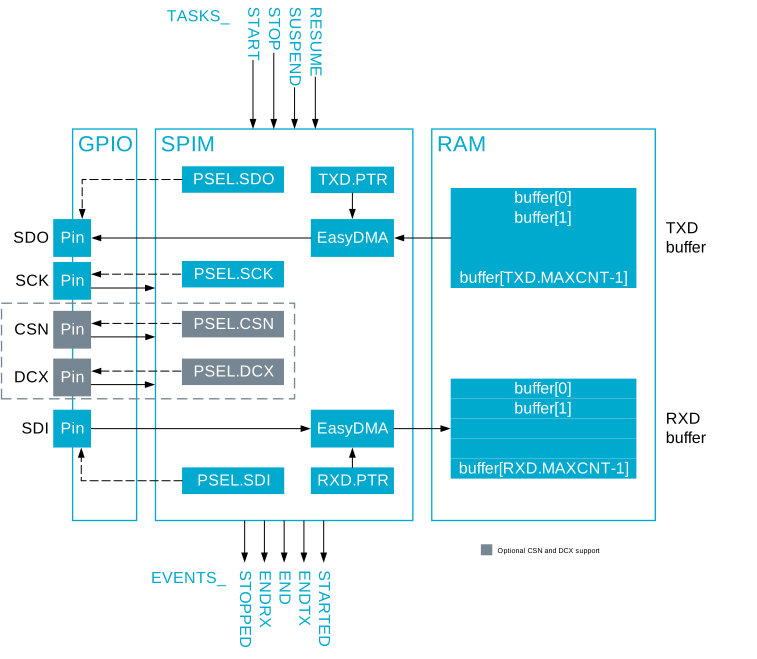
The SPI controller peripheral (SPIM) with EasyDMA provides a full duplex, 4-wire synchronous serial communication interface.
The main features of SPIM are the following:
- EasyDMA direct transfer to and from RAM
- SPI mode [0..3]
- Individual selection of I/O pins
- Optional D/CX output line for distinguishing between command and data bytes
- Optional hardware controlled chip select (CSN)
SPIM transaction sequence
An SPIM transaction is started by triggering the START task. This initiates a number of bytes to be transmitted/received on SDO/SDI.
The following figure illustrates an SPIM transaction.
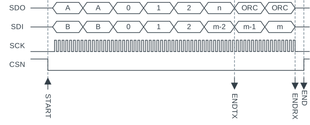
The ENDTX event is generated when all bytes in buffer DMA.TX.PTR are transmitted. The number of bytes in the transmit buffer is specified in register DMA.TX.MAXCNT. The ENDRX event is generated when buffer DMA.RX.PTR is full; that is when the number of bytes specified in register DMA.RX.MAXCNT have been received. The transaction stops automatically after all bytes are transmitted or received. When the maximum number of bytes in the receive buffer is larger than the number of bytes in the transmit buffer, the contents of register ORC will be transmitted after the last byte in the transmit buffer has been transmitted.
The END event is generated after both the ENDRX and ENDTX events have been generated.
SPIM is stopped by triggering the STOP task. A STOPPED event is generated when the SPIM has stopped. If the STOP task is triggered in the middle of a transaction, SPIM completes the process for the current byte before stopping. The STOPPED event is generated even if the STOP task is triggered while there is no ongoing transaction.
If the ENDTX event has not been generated when the SPIM peripheral stops, the ENDTX event will be generated, even if all bytes in the buffer have not been transmitted.
If the ENDRX event has not been generated when the SPIM stops, the ENDRX event will be generated even if the buffer DMA.RX.PTR is not full.
A transaction can be suspended and resumed using the SUSPEND and RESUME tasks, respectively. When the SUSPEND task is triggered, SPIM completes transmitting and receiving the current byte before it is suspended.
D/CX functionality
Some SPI targets, such as display drivers, require an additional signal from the SPIM to distinguish between command and data bytes. This line is called D/CX.
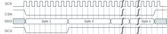
SPIM supports additional signals such as a D/CX output line. The D/CX line is set low for transmitting command bytes and high for transmitting data bytes.
The D/CX pin number is selected using . The number of command bytes that precede the data bytes is configured using DCXCNT. Writing to DCXCNT during an ongoing transmission is not allowed.
The following figure shows D/CX in use, where SPIM.DCXCNT=1.
Chip select hardware control
To use CSN hardware control, set register PSEL.CSN according to the Pin configuration.
When enabled, CSN is asserted automatically after TASKS_START is triggered, and deasserted after EVENTS_END. The value in register IFTIMING.CSNDUR sets the time between the falling edge of CSN and the first SCK edge. The same delay is used between the last SCK edge and the rising edge of CSN at the end of a transfer. It is also used between two transfers as the minimum CSN inactive time when the END_START short is enabled. The IFTIMING.CSNDUR is expressed in number of SPIM core clock periods.
The following figure shows a timing diagram with two SPI transmissions where the delay is controlled by IFTIMING.CSNDUR and is represented by tCSNDUR.
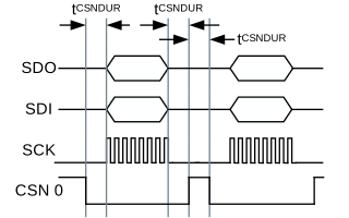
The following figure shows the timing delay for the combinations of polarity and phase settings. The register CSNPOL determines the active polarity of the signal.
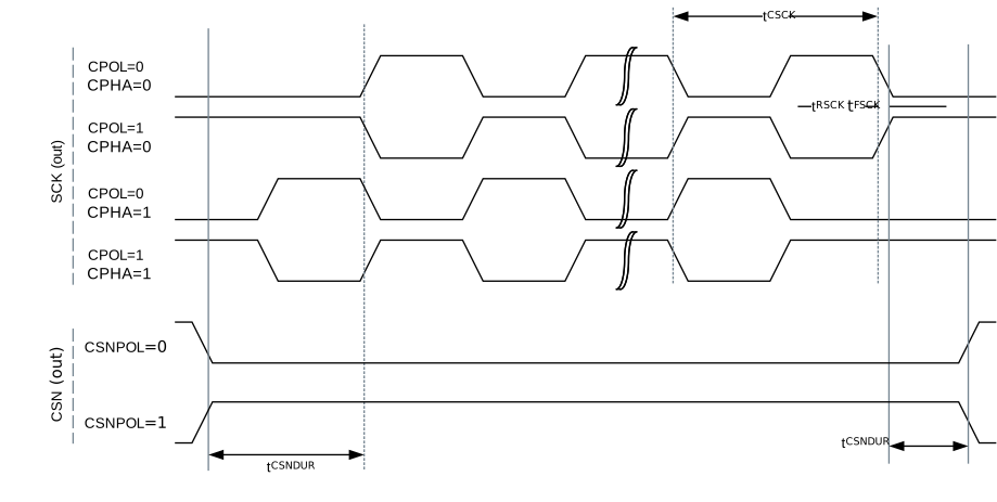
Pin configuration
To configure pins for SPIM use, see the corresponding PSEL.n registers.
The contents of registers PSEL.SCK, PSEL.CSN, PSEL.DCX, PSEL.MOSI, and PSEL.MISO are only used when SPIM is enabled, and retained while the device is in System ON mode. The PSEL.n registers can be configured only when SPIM is disabled in register ENABLE.
To ensure correct behavior, the pins used by SPIM must be configured in the GPIO peripheral as described in GPIO configuration before SPIM is enabled.
Only one peripheral can be assigned to drive a GPIO pin at a time. If more than one peripheral is assigned to a GPIO pin, it could result in unpredictable behavior.
| SPIM signal | SPIM pin | Direction | Output value |
|---|---|---|---|
| SCK | As specified in PSEL.SCK | Output | Same as CONFIG.CPOL |
| CSN | As specified in PSEL.CSN | Output | Same as CONFIG.CPOL |
| DCX | As specified in PSEL.DCX | Output | 1 |
| SDO | As specified in PSEL.MOSI | Output | 0 |
| SDI | As specified in PSEL.MISO | Input | Not applicable |
SPIM supports SPI modes [0..3]. The clock polarity (CPOL) and the clock phase (CPHA) are configured in register CONFIG.
| Mode | Clock polarity (CPOL) | Clock phase (CPHA) |
|---|---|---|
| SPI_MODE0 | 0 (Active High) | 0 (Leading) |
| SPI_MODE1 | 0 (Active High) | 1 (Trailing) |
| SPI_MODE2 | 1 (Active Low) | 0 (Leading) |
| SPI_MODE3 | 1 (Active Low) | 1 (Trailing) |
Shared resources
The SPIM peripheral shares registers and other resources with peripherals that have the same ID as SPIM. Before SPIM can be configured and used, all peripherals that have the same ID as SPIM must be disabled.
Disabling a peripheral with the same ID as SPIM will not reset any shared SPIM registers. Configure all SPIM registers to ensure they operate correctly.
See the Instantiation table in Instantiation for details on peripherals and their IDs.
EasyDMA
SPIM uses EasyDMA to fetch data to transmit from RAM or store received data in RAM.
| Channel | Type | Register Cluster |
|---|---|---|
| TXD | READER | DMA.TX.PTR |
| RXD | WRITER | DMA.RX.PTR |
The .PTR and .MAXCNT registers are double-buffered. After receiving the STARTED event, the registers can be written to before the next transmission.
SPIM automatically stops transmitting after TXD.MAXCNT bytes have been transmitted and RXD.MAXCNT bytes have been received. If RXD.MAXCNT is larger than TXD.MAXCNT, the remaining transmitted bytes will contain the value defined in the ORC register. If TXD.MAXCNT is larger than RXD.MAXCNT, the additional received bytes will be discarded.
The RX.END and TX.END events indicate that EasyDMA has finished accessing buffers in RAM. Both RX and TX must be finished before the END event is generated.
If several AHB bus masters try to access the same AHB slave at the same time, AHB bus congestion can occur. In this case, the EasyDMA channel behavior will depend on the SPIM instance. Refer to Instances for information about what behavior is expected in each instance.
See EasyDMA for more detailed information.
Low power
When the peripheral is not needed, stop and disable SPIM to ensure lowest possible power consumption.
When the STOP task is sent, the software must wait until the STOPPED event is received before disabling the peripheral through the ENABLE register. If the peripheral is already stopped, the STOP task is not needed to ensure data is not lost.
Registers
Instances
| Instance | Domain | Base address | Description |
|---|---|---|---|
| SPIM20 | GLOBAL | 0x400C6000 | SPI controller SPIM20 |
| SPIM21 | GLOBAL | 0x400C7000 | SPI controller SPIM21 |
| SPIM22 | GLOBAL | 0x400C8000 | SPI controller SPIM22 |
Configuration
| Instance | Domain | Configuration |
|---|---|---|
| SPIM20 | GLOBAL | Use GPIO port P1 CSN functionality is supported. DCX functionality is supported. Peripheral core frequency is 16 MHz. Prescaler divisor range is 2..126 |
| SPIM21 | GLOBAL | Use GPIO port P1 CSN functionality is supported. DCX functionality is supported. Peripheral core frequency is 16 MHz. Prescaler divisor range is 2..126 |
| SPIM22 | GLOBAL | Use GPIO port P1 CSN functionality is supported. DCX functionality is supported. Peripheral core frequency is 16 MHz. Prescaler divisor range is 2..126 |
Register overview
| Register | Offset | Description |
|---|---|---|
| TASKS_START | 0x000 | Start SPI transaction |
| TASKS_STOP | 0x004 | Stop SPI transaction |
| TASKS_SUSPEND | 0x00C | Suspend SPI transaction |
| TASKS_RESUME | 0x010 | Resume SPI transaction |
| TASKS_DMA.RX.ENABLEMATCH[n] | 0x030 | Enables the MATCH[n] event by setting the ENABLE[n] bit in the CONFIG register. |
| TASKS_DMA.RX.DISABLEMATCH[n] | 0x040 | Disables the MATCH[n] event by clearing the ENABLE[n] bit in the CONFIG register. |
| SUBSCRIBE_START | 0x080 | Subscribe configuration for task START |
| SUBSCRIBE_STOP | 0x084 | Subscribe configuration for task STOP |
| SUBSCRIBE_SUSPEND | 0x08C | Subscribe configuration for task SUSPEND |
| SUBSCRIBE_RESUME | 0x090 | Subscribe configuration for task RESUME |
| SUBSCRIBE_DMA.RX.ENABLEMATCH[n] | 0x0B0 | Subscribe configuration for task ENABLEMATCH[n] |
| SUBSCRIBE_DMA.RX.DISABLEMATCH[n] | 0x0C0 | Subscribe configuration for task DISABLEMATCH[n] |
| EVENTS_STARTED | 0x100 | SPI transaction has started |
| EVENTS_STOPPED | 0x104 | SPI transaction has stopped |
| EVENTS_END | 0x108 | End of RXD buffer and TXD buffer reached |
| EVENTS_DMA.RX.END | 0x14C | Generated after all MAXCNT bytes have been transferred |
| EVENTS_DMA.RX.READY | 0x150 | Generated when EasyDMA has buffered the .PTR and .MAXCNT registers for the channel, allowing them to be written to prepare for the next sequence. |
| EVENTS_DMA.RX.BUSERROR | 0x154 | An error occured during the bus transfer. |
| EVENTS_DMA.RX.MATCH[n] | 0x158 | Pattern match is detected on the DMA data bus. |
| EVENTS_DMA.TX.END | 0x168 | Generated after all MAXCNT bytes have been transferred |
| EVENTS_DMA.TX.READY | 0x16C | Generated when EasyDMA has buffered the .PTR and .MAXCNT registers for the channel, allowing them to be written to prepare for the next sequence. |
| EVENTS_DMA.TX.BUSERROR | 0x170 | An error occured during the bus transfer. |
| PUBLISH_STARTED | 0x180 | Publish configuration for event STARTED |
| PUBLISH_STOPPED | 0x184 | Publish configuration for event STOPPED |
| PUBLISH_END | 0x188 | Publish configuration for event END |
| PUBLISH_DMA.RX.END | 0x1CC | Publish configuration for event END |
| PUBLISH_DMA.RX.READY | 0x1D0 | Publish configuration for event READY |
| PUBLISH_DMA.RX.BUSERROR | 0x1D4 | Publish configuration for event BUSERROR |
| PUBLISH_DMA.RX.MATCH[n] | 0x1D8 | Publish configuration for event MATCH[n] |
| PUBLISH_DMA.TX.END | 0x1E8 | Publish configuration for event END |
| PUBLISH_DMA.TX.READY | 0x1EC | Publish configuration for event READY |
| PUBLISH_DMA.TX.BUSERROR | 0x1F0 | Publish configuration for event BUSERROR |
| SHORTS | 0x200 | Shortcuts between local events and tasks |
| INTENSET | 0x304 | Enable interrupt |
| INTENCLR | 0x308 | Disable interrupt |
| ENABLE | 0x500 | Enable SPIM |
| PRESCALER | 0x52C | The prescaler is used to set the SPI frequency. |
| CONFIG | 0x554 | Configuration register |
| IFTIMING.RXDELAY | 0x5AC | Sample delay for input serial data on SDI |
| IFTIMING.CSNDUR | 0x5B0 | Minimum duration between edge of CSN and edge of SCK. When SHORTS.END_START is used, this is also the minimum duration CSN must stay high between transactions. |
| DCXCNT | 0x5B4 | DCX configuration |
| CSNPOL | 0x5B8 | Polarity of CSN output |
| ORC | 0x5C0 | Byte transmitted after TXD.MAXCNT bytes have been transmitted in the case when RXD.MAXCNT is greater than TXD.MAXCNT |
| PSEL.SCK | 0x600 | Pin select for SCK |
| PSEL.MOSI | 0x604 | Pin select for SDO signal |
| PSEL.MISO | 0x608 | Pin select for SDI signal |
| PSEL.DCX | 0x60C | Pin select for DCX signal |
| PSEL.CSN | 0x610 | Pin select for CSN |
| DMA.RX.PTR | 0x704 | RAM buffer start address |
| DMA.RX.MAXCNT | 0x708 | Maximum number of bytes in channel buffer |
| DMA.RX.AMOUNT | 0x70C | Number of bytes transferred in the last transaction, updated after the END event. Also updated after each MATCH event. |
| DMA.RX.LIST | 0x714 | EasyDMA list type |
| DMA.RX.TERMINATEONBUSERROR | 0x71C | Terminate the transaction if a BUSERROR event is detected. |
| DMA.RX.BUSERRORADDRESS | 0x720 | Address of transaction that generated the last BUSERROR event. |
| DMA.RX.MATCH.CONFIG | 0x724 | Configure individual match events |
| DMA.RX.MATCH.CANDIDATE[n] | 0x728 | The data to look for - any match will trigger the MATCH[n] event, if enabled. |
| DMA.TX.PTR | 0x73C | RAM buffer start address |
| DMA.TX.MAXCNT | 0x740 | Maximum number of bytes in channel buffer |
| DMA.TX.AMOUNT | 0x744 | Number of bytes transferred in the last transaction, updated after the END event. Also updated after each MATCH event. |
| DMA.TX.LIST | 0x74C | EasyDMA list type |
| DMA.TX.TERMINATEONBUSERROR | 0x754 | Terminate the transaction if a BUSERROR event is detected. |
| DMA.TX.BUSERRORADDRESS | 0x758 | Address of transaction that generated the last BUSERROR event. |
TASKS_START
Address offset: 0x000
Start SPI transaction
| Bit number | 31 | 30 | 29 | 28 | 27 | 26 | 25 | 24 | 23 | 22 | 21 | 20 | 19 | 18 | 17 | 16 | 15 | 14 | 13 | 12 | 11 | 10 | 9 | 8 | 7 | 6 | 5 | 4 | 3 | 2 | 1 | 0 | |||
|---|---|---|---|---|---|---|---|---|---|---|---|---|---|---|---|---|---|---|---|---|---|---|---|---|---|---|---|---|---|---|---|---|---|---|---|
| ID | A | ||||||||||||||||||||||||||||||||||
| Reset 0x00000000 | 0 | 0 | 0 | 0 | 0 | 0 | 0 | 0 | 0 | 0 | 0 | 0 | 0 | 0 | 0 | 0 | 0 | 0 | 0 | 0 | 0 | 0 | 0 | 0 | 0 | 0 | 0 | 0 | 0 | 0 | 0 | 0 | |||
| ID | R/W | Field | Value ID | Value | Description | ||||||||||||||||||||||||||||||
| A | W | TASKS_START | Start SPI transaction | ||||||||||||||||||||||||||||||||
Trigger | 1 | Trigger task | |||||||||||||||||||||||||||||||||
TASKS_STOP
Address offset: 0x004
Stop SPI transaction
| Bit number | 31 | 30 | 29 | 28 | 27 | 26 | 25 | 24 | 23 | 22 | 21 | 20 | 19 | 18 | 17 | 16 | 15 | 14 | 13 | 12 | 11 | 10 | 9 | 8 | 7 | 6 | 5 | 4 | 3 | 2 | 1 | 0 | |||
|---|---|---|---|---|---|---|---|---|---|---|---|---|---|---|---|---|---|---|---|---|---|---|---|---|---|---|---|---|---|---|---|---|---|---|---|
| ID | A | ||||||||||||||||||||||||||||||||||
| Reset 0x00000000 | 0 | 0 | 0 | 0 | 0 | 0 | 0 | 0 | 0 | 0 | 0 | 0 | 0 | 0 | 0 | 0 | 0 | 0 | 0 | 0 | 0 | 0 | 0 | 0 | 0 | 0 | 0 | 0 | 0 | 0 | 0 | 0 | |||
| ID | R/W | Field | Value ID | Value | Description | ||||||||||||||||||||||||||||||
| A | W | TASKS_STOP | Stop SPI transaction | ||||||||||||||||||||||||||||||||
Trigger | 1 | Trigger task | |||||||||||||||||||||||||||||||||
TASKS_SUSPEND
Address offset: 0x00C
Suspend SPI transaction
| Bit number | 31 | 30 | 29 | 28 | 27 | 26 | 25 | 24 | 23 | 22 | 21 | 20 | 19 | 18 | 17 | 16 | 15 | 14 | 13 | 12 | 11 | 10 | 9 | 8 | 7 | 6 | 5 | 4 | 3 | 2 | 1 | 0 | |||
|---|---|---|---|---|---|---|---|---|---|---|---|---|---|---|---|---|---|---|---|---|---|---|---|---|---|---|---|---|---|---|---|---|---|---|---|
| ID | A | ||||||||||||||||||||||||||||||||||
| Reset 0x00000000 | 0 | 0 | 0 | 0 | 0 | 0 | 0 | 0 | 0 | 0 | 0 | 0 | 0 | 0 | 0 | 0 | 0 | 0 | 0 | 0 | 0 | 0 | 0 | 0 | 0 | 0 | 0 | 0 | 0 | 0 | 0 | 0 | |||
| ID | R/W | Field | Value ID | Value | Description | ||||||||||||||||||||||||||||||
| A | W | TASKS_SUSPEND | Suspend SPI transaction | ||||||||||||||||||||||||||||||||
Trigger | 1 | Trigger task | |||||||||||||||||||||||||||||||||
TASKS_RESUME
Address offset: 0x010
Resume SPI transaction
| Bit number | 31 | 30 | 29 | 28 | 27 | 26 | 25 | 24 | 23 | 22 | 21 | 20 | 19 | 18 | 17 | 16 | 15 | 14 | 13 | 12 | 11 | 10 | 9 | 8 | 7 | 6 | 5 | 4 | 3 | 2 | 1 | 0 | |||
|---|---|---|---|---|---|---|---|---|---|---|---|---|---|---|---|---|---|---|---|---|---|---|---|---|---|---|---|---|---|---|---|---|---|---|---|
| ID | A | ||||||||||||||||||||||||||||||||||
| Reset 0x00000000 | 0 | 0 | 0 | 0 | 0 | 0 | 0 | 0 | 0 | 0 | 0 | 0 | 0 | 0 | 0 | 0 | 0 | 0 | 0 | 0 | 0 | 0 | 0 | 0 | 0 | 0 | 0 | 0 | 0 | 0 | 0 | 0 | |||
| ID | R/W | Field | Value ID | Value | Description | ||||||||||||||||||||||||||||||
| A | W | TASKS_RESUME | Resume SPI transaction | ||||||||||||||||||||||||||||||||
Trigger | 1 | Trigger task | |||||||||||||||||||||||||||||||||
TASKS_DMA
Peripheral tasks.
TASKS_DMA.RX
Peripheral tasks.
TASKS_DMA.RX.ENABLEMATCH[n]
Address offset: 0x030 + (n × 0x4)
Enables the MATCH[n] event by setting the ENABLE[n] bit in the CONFIG register.
| Bit number | 31 | 30 | 29 | 28 | 27 | 26 | 25 | 24 | 23 | 22 | 21 | 20 | 19 | 18 | 17 | 16 | 15 | 14 | 13 | 12 | 11 | 10 | 9 | 8 | 7 | 6 | 5 | 4 | 3 | 2 | 1 | 0 | |||
|---|---|---|---|---|---|---|---|---|---|---|---|---|---|---|---|---|---|---|---|---|---|---|---|---|---|---|---|---|---|---|---|---|---|---|---|
| ID | A | ||||||||||||||||||||||||||||||||||
| Reset 0x00000000 | 0 | 0 | 0 | 0 | 0 | 0 | 0 | 0 | 0 | 0 | 0 | 0 | 0 | 0 | 0 | 0 | 0 | 0 | 0 | 0 | 0 | 0 | 0 | 0 | 0 | 0 | 0 | 0 | 0 | 0 | 0 | 0 | |||
| ID | R/W | Field | Value ID | Value | Description | ||||||||||||||||||||||||||||||
| A | W | ENABLEMATCH | Enables the MATCH[n] event by setting the ENABLE[n] bit in the CONFIG register. | ||||||||||||||||||||||||||||||||
Trigger | 1 | Trigger task | |||||||||||||||||||||||||||||||||
TASKS_DMA.RX.DISABLEMATCH[n]
Address offset: 0x040 + (n × 0x4)
Disables the MATCH[n] event by clearing the ENABLE[n] bit in the CONFIG register.
| Bit number | 31 | 30 | 29 | 28 | 27 | 26 | 25 | 24 | 23 | 22 | 21 | 20 | 19 | 18 | 17 | 16 | 15 | 14 | 13 | 12 | 11 | 10 | 9 | 8 | 7 | 6 | 5 | 4 | 3 | 2 | 1 | 0 | |||
|---|---|---|---|---|---|---|---|---|---|---|---|---|---|---|---|---|---|---|---|---|---|---|---|---|---|---|---|---|---|---|---|---|---|---|---|
| ID | A | ||||||||||||||||||||||||||||||||||
| Reset 0x00000000 | 0 | 0 | 0 | 0 | 0 | 0 | 0 | 0 | 0 | 0 | 0 | 0 | 0 | 0 | 0 | 0 | 0 | 0 | 0 | 0 | 0 | 0 | 0 | 0 | 0 | 0 | 0 | 0 | 0 | 0 | 0 | 0 | |||
| ID | R/W | Field | Value ID | Value | Description | ||||||||||||||||||||||||||||||
| A | W | DISABLEMATCH | Disables the MATCH[n] event by clearing the ENABLE[n] bit in the CONFIG register. | ||||||||||||||||||||||||||||||||
Trigger | 1 | Trigger task | |||||||||||||||||||||||||||||||||
SUBSCRIBE_START
Address offset: 0x080
Subscribe configuration for task START
| Bit number | 31 | 30 | 29 | 28 | 27 | 26 | 25 | 24 | 23 | 22 | 21 | 20 | 19 | 18 | 17 | 16 | 15 | 14 | 13 | 12 | 11 | 10 | 9 | 8 | 7 | 6 | 5 | 4 | 3 | 2 | 1 | 0 | |||
|---|---|---|---|---|---|---|---|---|---|---|---|---|---|---|---|---|---|---|---|---|---|---|---|---|---|---|---|---|---|---|---|---|---|---|---|
| ID | B | A | A | A | A | A | A | A | A | ||||||||||||||||||||||||||
| Reset 0x00000000 | 0 | 0 | 0 | 0 | 0 | 0 | 0 | 0 | 0 | 0 | 0 | 0 | 0 | 0 | 0 | 0 | 0 | 0 | 0 | 0 | 0 | 0 | 0 | 0 | 0 | 0 | 0 | 0 | 0 | 0 | 0 | 0 | |||
| ID | R/W | Field | Value ID | Value | Description | ||||||||||||||||||||||||||||||
| A | RW | CHIDX | [0..255] | DPPI channel that task START will subscribe to | |||||||||||||||||||||||||||||||
| B | RW | EN | |||||||||||||||||||||||||||||||||
Disabled | 0 | Disable subscription | |||||||||||||||||||||||||||||||||
Enabled | 1 | Enable subscription | |||||||||||||||||||||||||||||||||
SUBSCRIBE_STOP
Address offset: 0x084
Subscribe configuration for task STOP
| Bit number | 31 | 30 | 29 | 28 | 27 | 26 | 25 | 24 | 23 | 22 | 21 | 20 | 19 | 18 | 17 | 16 | 15 | 14 | 13 | 12 | 11 | 10 | 9 | 8 | 7 | 6 | 5 | 4 | 3 | 2 | 1 | 0 | |||
|---|---|---|---|---|---|---|---|---|---|---|---|---|---|---|---|---|---|---|---|---|---|---|---|---|---|---|---|---|---|---|---|---|---|---|---|
| ID | B | A | A | A | A | A | A | A | A | ||||||||||||||||||||||||||
| Reset 0x00000000 | 0 | 0 | 0 | 0 | 0 | 0 | 0 | 0 | 0 | 0 | 0 | 0 | 0 | 0 | 0 | 0 | 0 | 0 | 0 | 0 | 0 | 0 | 0 | 0 | 0 | 0 | 0 | 0 | 0 | 0 | 0 | 0 | |||
| ID | R/W | Field | Value ID | Value | Description | ||||||||||||||||||||||||||||||
| A | RW | CHIDX | [0..255] | DPPI channel that task STOP will subscribe to | |||||||||||||||||||||||||||||||
| B | RW | EN | |||||||||||||||||||||||||||||||||
Disabled | 0 | Disable subscription | |||||||||||||||||||||||||||||||||
Enabled | 1 | Enable subscription | |||||||||||||||||||||||||||||||||
SUBSCRIBE_SUSPEND
Address offset: 0x08C
Subscribe configuration for task SUSPEND
| Bit number | 31 | 30 | 29 | 28 | 27 | 26 | 25 | 24 | 23 | 22 | 21 | 20 | 19 | 18 | 17 | 16 | 15 | 14 | 13 | 12 | 11 | 10 | 9 | 8 | 7 | 6 | 5 | 4 | 3 | 2 | 1 | 0 | |||
|---|---|---|---|---|---|---|---|---|---|---|---|---|---|---|---|---|---|---|---|---|---|---|---|---|---|---|---|---|---|---|---|---|---|---|---|
| ID | B | A | A | A | A | A | A | A | A | ||||||||||||||||||||||||||
| Reset 0x00000000 | 0 | 0 | 0 | 0 | 0 | 0 | 0 | 0 | 0 | 0 | 0 | 0 | 0 | 0 | 0 | 0 | 0 | 0 | 0 | 0 | 0 | 0 | 0 | 0 | 0 | 0 | 0 | 0 | 0 | 0 | 0 | 0 | |||
| ID | R/W | Field | Value ID | Value | Description | ||||||||||||||||||||||||||||||
| A | RW | CHIDX | [0..255] | DPPI channel that task SUSPEND will subscribe to | |||||||||||||||||||||||||||||||
| B | RW | EN | |||||||||||||||||||||||||||||||||
Disabled | 0 | Disable subscription | |||||||||||||||||||||||||||||||||
Enabled | 1 | Enable subscription | |||||||||||||||||||||||||||||||||
SUBSCRIBE_RESUME
Address offset: 0x090
Subscribe configuration for task RESUME
| Bit number | 31 | 30 | 29 | 28 | 27 | 26 | 25 | 24 | 23 | 22 | 21 | 20 | 19 | 18 | 17 | 16 | 15 | 14 | 13 | 12 | 11 | 10 | 9 | 8 | 7 | 6 | 5 | 4 | 3 | 2 | 1 | 0 | |||
|---|---|---|---|---|---|---|---|---|---|---|---|---|---|---|---|---|---|---|---|---|---|---|---|---|---|---|---|---|---|---|---|---|---|---|---|
| ID | B | A | A | A | A | A | A | A | A | ||||||||||||||||||||||||||
| Reset 0x00000000 | 0 | 0 | 0 | 0 | 0 | 0 | 0 | 0 | 0 | 0 | 0 | 0 | 0 | 0 | 0 | 0 | 0 | 0 | 0 | 0 | 0 | 0 | 0 | 0 | 0 | 0 | 0 | 0 | 0 | 0 | 0 | 0 | |||
| ID | R/W | Field | Value ID | Value | Description | ||||||||||||||||||||||||||||||
| A | RW | CHIDX | [0..255] | DPPI channel that task RESUME will subscribe to | |||||||||||||||||||||||||||||||
| B | RW | EN | |||||||||||||||||||||||||||||||||
Disabled | 0 | Disable subscription | |||||||||||||||||||||||||||||||||
Enabled | 1 | Enable subscription | |||||||||||||||||||||||||||||||||
SUBSCRIBE_DMA
Subscribe configuration for tasks
SUBSCRIBE_DMA.RX
Subscribe configuration for tasks
SUBSCRIBE_DMA.RX.ENABLEMATCH[n]
Address offset: 0x0B0 + (n × 0x4)
Subscribe configuration for task ENABLEMATCH[n]
| Bit number | 31 | 30 | 29 | 28 | 27 | 26 | 25 | 24 | 23 | 22 | 21 | 20 | 19 | 18 | 17 | 16 | 15 | 14 | 13 | 12 | 11 | 10 | 9 | 8 | 7 | 6 | 5 | 4 | 3 | 2 | 1 | 0 | |||
|---|---|---|---|---|---|---|---|---|---|---|---|---|---|---|---|---|---|---|---|---|---|---|---|---|---|---|---|---|---|---|---|---|---|---|---|
| ID | B | A | A | A | A | A | A | A | A | ||||||||||||||||||||||||||
| Reset 0x00000000 | 0 | 0 | 0 | 0 | 0 | 0 | 0 | 0 | 0 | 0 | 0 | 0 | 0 | 0 | 0 | 0 | 0 | 0 | 0 | 0 | 0 | 0 | 0 | 0 | 0 | 0 | 0 | 0 | 0 | 0 | 0 | 0 | |||
| ID | R/W | Field | Value ID | Value | Description | ||||||||||||||||||||||||||||||
| A | RW | CHIDX | [0..255] | DPPI channel that task ENABLEMATCH[n] will subscribe to | |||||||||||||||||||||||||||||||
| B | RW | EN | |||||||||||||||||||||||||||||||||
Disabled | 0 | Disable subscription | |||||||||||||||||||||||||||||||||
Enabled | 1 | Enable subscription | |||||||||||||||||||||||||||||||||
SUBSCRIBE_DMA.RX.DISABLEMATCH[n]
Address offset: 0x0C0 + (n × 0x4)
Subscribe configuration for task DISABLEMATCH[n]
| Bit number | 31 | 30 | 29 | 28 | 27 | 26 | 25 | 24 | 23 | 22 | 21 | 20 | 19 | 18 | 17 | 16 | 15 | 14 | 13 | 12 | 11 | 10 | 9 | 8 | 7 | 6 | 5 | 4 | 3 | 2 | 1 | 0 | |||
|---|---|---|---|---|---|---|---|---|---|---|---|---|---|---|---|---|---|---|---|---|---|---|---|---|---|---|---|---|---|---|---|---|---|---|---|
| ID | B | A | A | A | A | A | A | A | A | ||||||||||||||||||||||||||
| Reset 0x00000000 | 0 | 0 | 0 | 0 | 0 | 0 | 0 | 0 | 0 | 0 | 0 | 0 | 0 | 0 | 0 | 0 | 0 | 0 | 0 | 0 | 0 | 0 | 0 | 0 | 0 | 0 | 0 | 0 | 0 | 0 | 0 | 0 | |||
| ID | R/W | Field | Value ID | Value | Description | ||||||||||||||||||||||||||||||
| A | RW | CHIDX | [0..255] | DPPI channel that task DISABLEMATCH[n] will subscribe to | |||||||||||||||||||||||||||||||
| B | RW | EN | |||||||||||||||||||||||||||||||||
Disabled | 0 | Disable subscription | |||||||||||||||||||||||||||||||||
Enabled | 1 | Enable subscription | |||||||||||||||||||||||||||||||||
EVENTS_STARTED
Address offset: 0x100
SPI transaction has started
| Bit number | 31 | 30 | 29 | 28 | 27 | 26 | 25 | 24 | 23 | 22 | 21 | 20 | 19 | 18 | 17 | 16 | 15 | 14 | 13 | 12 | 11 | 10 | 9 | 8 | 7 | 6 | 5 | 4 | 3 | 2 | 1 | 0 | |||
|---|---|---|---|---|---|---|---|---|---|---|---|---|---|---|---|---|---|---|---|---|---|---|---|---|---|---|---|---|---|---|---|---|---|---|---|
| ID | A | ||||||||||||||||||||||||||||||||||
| Reset 0x00000000 | 0 | 0 | 0 | 0 | 0 | 0 | 0 | 0 | 0 | 0 | 0 | 0 | 0 | 0 | 0 | 0 | 0 | 0 | 0 | 0 | 0 | 0 | 0 | 0 | 0 | 0 | 0 | 0 | 0 | 0 | 0 | 0 | |||
| ID | R/W | Field | Value ID | Value | Description | ||||||||||||||||||||||||||||||
| A | RW | EVENTS_STARTED | SPI transaction has started | ||||||||||||||||||||||||||||||||
NotGenerated | 0 | Event not generated | |||||||||||||||||||||||||||||||||
Generated | 1 | Event generated | |||||||||||||||||||||||||||||||||
EVENTS_STOPPED
Address offset: 0x104
SPI transaction has stopped
| Bit number | 31 | 30 | 29 | 28 | 27 | 26 | 25 | 24 | 23 | 22 | 21 | 20 | 19 | 18 | 17 | 16 | 15 | 14 | 13 | 12 | 11 | 10 | 9 | 8 | 7 | 6 | 5 | 4 | 3 | 2 | 1 | 0 | |||
|---|---|---|---|---|---|---|---|---|---|---|---|---|---|---|---|---|---|---|---|---|---|---|---|---|---|---|---|---|---|---|---|---|---|---|---|
| ID | A | ||||||||||||||||||||||||||||||||||
| Reset 0x00000000 | 0 | 0 | 0 | 0 | 0 | 0 | 0 | 0 | 0 | 0 | 0 | 0 | 0 | 0 | 0 | 0 | 0 | 0 | 0 | 0 | 0 | 0 | 0 | 0 | 0 | 0 | 0 | 0 | 0 | 0 | 0 | 0 | |||
| ID | R/W | Field | Value ID | Value | Description | ||||||||||||||||||||||||||||||
| A | RW | EVENTS_STOPPED | SPI transaction has stopped | ||||||||||||||||||||||||||||||||
NotGenerated | 0 | Event not generated | |||||||||||||||||||||||||||||||||
Generated | 1 | Event generated | |||||||||||||||||||||||||||||||||
EVENTS_END
Address offset: 0x108
End of RXD buffer and TXD buffer reached
| Bit number | 31 | 30 | 29 | 28 | 27 | 26 | 25 | 24 | 23 | 22 | 21 | 20 | 19 | 18 | 17 | 16 | 15 | 14 | 13 | 12 | 11 | 10 | 9 | 8 | 7 | 6 | 5 | 4 | 3 | 2 | 1 | 0 | |||
|---|---|---|---|---|---|---|---|---|---|---|---|---|---|---|---|---|---|---|---|---|---|---|---|---|---|---|---|---|---|---|---|---|---|---|---|
| ID | A | ||||||||||||||||||||||||||||||||||
| Reset 0x00000000 | 0 | 0 | 0 | 0 | 0 | 0 | 0 | 0 | 0 | 0 | 0 | 0 | 0 | 0 | 0 | 0 | 0 | 0 | 0 | 0 | 0 | 0 | 0 | 0 | 0 | 0 | 0 | 0 | 0 | 0 | 0 | 0 | |||
| ID | R/W | Field | Value ID | Value | Description | ||||||||||||||||||||||||||||||
| A | RW | EVENTS_END | End of RXD buffer and TXD buffer reached | ||||||||||||||||||||||||||||||||
NotGenerated | 0 | Event not generated | |||||||||||||||||||||||||||||||||
Generated | 1 | Event generated | |||||||||||||||||||||||||||||||||
EVENTS_DMA
Peripheral events.
EVENTS_DMA.RX
Peripheral events.
EVENTS_DMA.RX.END
Address offset: 0x14C
Generated after all MAXCNT bytes have been transferred
| Bit number | 31 | 30 | 29 | 28 | 27 | 26 | 25 | 24 | 23 | 22 | 21 | 20 | 19 | 18 | 17 | 16 | 15 | 14 | 13 | 12 | 11 | 10 | 9 | 8 | 7 | 6 | 5 | 4 | 3 | 2 | 1 | 0 | |||
|---|---|---|---|---|---|---|---|---|---|---|---|---|---|---|---|---|---|---|---|---|---|---|---|---|---|---|---|---|---|---|---|---|---|---|---|
| ID | A | ||||||||||||||||||||||||||||||||||
| Reset 0x00000000 | 0 | 0 | 0 | 0 | 0 | 0 | 0 | 0 | 0 | 0 | 0 | 0 | 0 | 0 | 0 | 0 | 0 | 0 | 0 | 0 | 0 | 0 | 0 | 0 | 0 | 0 | 0 | 0 | 0 | 0 | 0 | 0 | |||
| ID | R/W | Field | Value ID | Value | Description | ||||||||||||||||||||||||||||||
| A | RW | END | Generated after all MAXCNT bytes have been transferred | ||||||||||||||||||||||||||||||||
NotGenerated | 0 | Event not generated | |||||||||||||||||||||||||||||||||
Generated | 1 | Event generated | |||||||||||||||||||||||||||||||||
EVENTS_DMA.RX.READY
Address offset: 0x150
Generated when EasyDMA has buffered the .PTR and .MAXCNT registers for the channel, allowing them to be written to prepare for the next sequence.
| Bit number | 31 | 30 | 29 | 28 | 27 | 26 | 25 | 24 | 23 | 22 | 21 | 20 | 19 | 18 | 17 | 16 | 15 | 14 | 13 | 12 | 11 | 10 | 9 | 8 | 7 | 6 | 5 | 4 | 3 | 2 | 1 | 0 | |||
|---|---|---|---|---|---|---|---|---|---|---|---|---|---|---|---|---|---|---|---|---|---|---|---|---|---|---|---|---|---|---|---|---|---|---|---|
| ID | A | ||||||||||||||||||||||||||||||||||
| Reset 0x00000000 | 0 | 0 | 0 | 0 | 0 | 0 | 0 | 0 | 0 | 0 | 0 | 0 | 0 | 0 | 0 | 0 | 0 | 0 | 0 | 0 | 0 | 0 | 0 | 0 | 0 | 0 | 0 | 0 | 0 | 0 | 0 | 0 | |||
| ID | R/W | Field | Value ID | Value | Description | ||||||||||||||||||||||||||||||
| A | RW | READY | Generated when EasyDMA has buffered the .PTR and .MAXCNT registers for the channel, allowing them to be written to prepare for the next sequence. | ||||||||||||||||||||||||||||||||
NotGenerated | 0 | Event not generated | |||||||||||||||||||||||||||||||||
Generated | 1 | Event generated | |||||||||||||||||||||||||||||||||
EVENTS_DMA.RX.BUSERROR
Address offset: 0x154
An error occured during the bus transfer.
When this event is generated, the address which caused the error can be read from the BUSERRORADDRESS register.
| Bit number | 31 | 30 | 29 | 28 | 27 | 26 | 25 | 24 | 23 | 22 | 21 | 20 | 19 | 18 | 17 | 16 | 15 | 14 | 13 | 12 | 11 | 10 | 9 | 8 | 7 | 6 | 5 | 4 | 3 | 2 | 1 | 0 | |||
|---|---|---|---|---|---|---|---|---|---|---|---|---|---|---|---|---|---|---|---|---|---|---|---|---|---|---|---|---|---|---|---|---|---|---|---|
| ID | A | ||||||||||||||||||||||||||||||||||
| Reset 0x00000000 | 0 | 0 | 0 | 0 | 0 | 0 | 0 | 0 | 0 | 0 | 0 | 0 | 0 | 0 | 0 | 0 | 0 | 0 | 0 | 0 | 0 | 0 | 0 | 0 | 0 | 0 | 0 | 0 | 0 | 0 | 0 | 0 | |||
| ID | R/W | Field | Value ID | Value | Description | ||||||||||||||||||||||||||||||
| A | RW | BUSERROR | An error occured during the bus transfer. When this event is generated, the address which caused the error can be read from the BUSERRORADDRESS register. | ||||||||||||||||||||||||||||||||
NotGenerated | 0 | Event not generated | |||||||||||||||||||||||||||||||||
Generated | 1 | Event generated | |||||||||||||||||||||||||||||||||
EVENTS_DMA.RX.MATCH[n]
Address offset: 0x158 + (n × 0x4)
Pattern match is detected on the DMA data bus.
| Bit number | 31 | 30 | 29 | 28 | 27 | 26 | 25 | 24 | 23 | 22 | 21 | 20 | 19 | 18 | 17 | 16 | 15 | 14 | 13 | 12 | 11 | 10 | 9 | 8 | 7 | 6 | 5 | 4 | 3 | 2 | 1 | 0 | |||
|---|---|---|---|---|---|---|---|---|---|---|---|---|---|---|---|---|---|---|---|---|---|---|---|---|---|---|---|---|---|---|---|---|---|---|---|
| ID | A | ||||||||||||||||||||||||||||||||||
| Reset 0x00000000 | 0 | 0 | 0 | 0 | 0 | 0 | 0 | 0 | 0 | 0 | 0 | 0 | 0 | 0 | 0 | 0 | 0 | 0 | 0 | 0 | 0 | 0 | 0 | 0 | 0 | 0 | 0 | 0 | 0 | 0 | 0 | 0 | |||
| ID | R/W | Field | Value ID | Value | Description | ||||||||||||||||||||||||||||||
| A | RW | MATCH | Pattern match is detected on the DMA data bus. | ||||||||||||||||||||||||||||||||
NotGenerated | 0 | Event not generated | |||||||||||||||||||||||||||||||||
Generated | 1 | Event generated | |||||||||||||||||||||||||||||||||
EVENTS_DMA.TX
Peripheral events.
EVENTS_DMA.TX.END
Address offset: 0x168
Generated after all MAXCNT bytes have been transferred
| Bit number | 31 | 30 | 29 | 28 | 27 | 26 | 25 | 24 | 23 | 22 | 21 | 20 | 19 | 18 | 17 | 16 | 15 | 14 | 13 | 12 | 11 | 10 | 9 | 8 | 7 | 6 | 5 | 4 | 3 | 2 | 1 | 0 | |||
|---|---|---|---|---|---|---|---|---|---|---|---|---|---|---|---|---|---|---|---|---|---|---|---|---|---|---|---|---|---|---|---|---|---|---|---|
| ID | A | ||||||||||||||||||||||||||||||||||
| Reset 0x00000000 | 0 | 0 | 0 | 0 | 0 | 0 | 0 | 0 | 0 | 0 | 0 | 0 | 0 | 0 | 0 | 0 | 0 | 0 | 0 | 0 | 0 | 0 | 0 | 0 | 0 | 0 | 0 | 0 | 0 | 0 | 0 | 0 | |||
| ID | R/W | Field | Value ID | Value | Description | ||||||||||||||||||||||||||||||
| A | RW | END | Generated after all MAXCNT bytes have been transferred | ||||||||||||||||||||||||||||||||
NotGenerated | 0 | Event not generated | |||||||||||||||||||||||||||||||||
Generated | 1 | Event generated | |||||||||||||||||||||||||||||||||
EVENTS_DMA.TX.READY
Address offset: 0x16C
Generated when EasyDMA has buffered the .PTR and .MAXCNT registers for the channel, allowing them to be written to prepare for the next sequence.
| Bit number | 31 | 30 | 29 | 28 | 27 | 26 | 25 | 24 | 23 | 22 | 21 | 20 | 19 | 18 | 17 | 16 | 15 | 14 | 13 | 12 | 11 | 10 | 9 | 8 | 7 | 6 | 5 | 4 | 3 | 2 | 1 | 0 | |||
|---|---|---|---|---|---|---|---|---|---|---|---|---|---|---|---|---|---|---|---|---|---|---|---|---|---|---|---|---|---|---|---|---|---|---|---|
| ID | A | ||||||||||||||||||||||||||||||||||
| Reset 0x00000000 | 0 | 0 | 0 | 0 | 0 | 0 | 0 | 0 | 0 | 0 | 0 | 0 | 0 | 0 | 0 | 0 | 0 | 0 | 0 | 0 | 0 | 0 | 0 | 0 | 0 | 0 | 0 | 0 | 0 | 0 | 0 | 0 | |||
| ID | R/W | Field | Value ID | Value | Description | ||||||||||||||||||||||||||||||
| A | RW | READY | Generated when EasyDMA has buffered the .PTR and .MAXCNT registers for the channel, allowing them to be written to prepare for the next sequence. | ||||||||||||||||||||||||||||||||
NotGenerated | 0 | Event not generated | |||||||||||||||||||||||||||||||||
Generated | 1 | Event generated | |||||||||||||||||||||||||||||||||
EVENTS_DMA.TX.BUSERROR
Address offset: 0x170
An error occured during the bus transfer.
When this event is generated, the address which caused the error can be read from the BUSERRORADDRESS register.
| Bit number | 31 | 30 | 29 | 28 | 27 | 26 | 25 | 24 | 23 | 22 | 21 | 20 | 19 | 18 | 17 | 16 | 15 | 14 | 13 | 12 | 11 | 10 | 9 | 8 | 7 | 6 | 5 | 4 | 3 | 2 | 1 | 0 | |||
|---|---|---|---|---|---|---|---|---|---|---|---|---|---|---|---|---|---|---|---|---|---|---|---|---|---|---|---|---|---|---|---|---|---|---|---|
| ID | A | ||||||||||||||||||||||||||||||||||
| Reset 0x00000000 | 0 | 0 | 0 | 0 | 0 | 0 | 0 | 0 | 0 | 0 | 0 | 0 | 0 | 0 | 0 | 0 | 0 | 0 | 0 | 0 | 0 | 0 | 0 | 0 | 0 | 0 | 0 | 0 | 0 | 0 | 0 | 0 | |||
| ID | R/W | Field | Value ID | Value | Description | ||||||||||||||||||||||||||||||
| A | RW | BUSERROR | An error occured during the bus transfer. When this event is generated, the address which caused the error can be read from the BUSERRORADDRESS register. | ||||||||||||||||||||||||||||||||
NotGenerated | 0 | Event not generated | |||||||||||||||||||||||||||||||||
Generated | 1 | Event generated | |||||||||||||||||||||||||||||||||
PUBLISH_STARTED
Address offset: 0x180
Publish configuration for event STARTED
| Bit number | 31 | 30 | 29 | 28 | 27 | 26 | 25 | 24 | 23 | 22 | 21 | 20 | 19 | 18 | 17 | 16 | 15 | 14 | 13 | 12 | 11 | 10 | 9 | 8 | 7 | 6 | 5 | 4 | 3 | 2 | 1 | 0 | |||
|---|---|---|---|---|---|---|---|---|---|---|---|---|---|---|---|---|---|---|---|---|---|---|---|---|---|---|---|---|---|---|---|---|---|---|---|
| ID | B | A | A | A | A | A | A | A | A | ||||||||||||||||||||||||||
| Reset 0x00000000 | 0 | 0 | 0 | 0 | 0 | 0 | 0 | 0 | 0 | 0 | 0 | 0 | 0 | 0 | 0 | 0 | 0 | 0 | 0 | 0 | 0 | 0 | 0 | 0 | 0 | 0 | 0 | 0 | 0 | 0 | 0 | 0 | |||
| ID | R/W | Field | Value ID | Value | Description | ||||||||||||||||||||||||||||||
| A | RW | CHIDX | [0..255] | DPPI channel that event STARTED will publish to | |||||||||||||||||||||||||||||||
| B | RW | EN | |||||||||||||||||||||||||||||||||
Disabled | 0 | Disable publishing | |||||||||||||||||||||||||||||||||
Enabled | 1 | Enable publishing | |||||||||||||||||||||||||||||||||
PUBLISH_STOPPED
Address offset: 0x184
Publish configuration for event STOPPED
| Bit number | 31 | 30 | 29 | 28 | 27 | 26 | 25 | 24 | 23 | 22 | 21 | 20 | 19 | 18 | 17 | 16 | 15 | 14 | 13 | 12 | 11 | 10 | 9 | 8 | 7 | 6 | 5 | 4 | 3 | 2 | 1 | 0 | |||
|---|---|---|---|---|---|---|---|---|---|---|---|---|---|---|---|---|---|---|---|---|---|---|---|---|---|---|---|---|---|---|---|---|---|---|---|
| ID | B | A | A | A | A | A | A | A | A | ||||||||||||||||||||||||||
| Reset 0x00000000 | 0 | 0 | 0 | 0 | 0 | 0 | 0 | 0 | 0 | 0 | 0 | 0 | 0 | 0 | 0 | 0 | 0 | 0 | 0 | 0 | 0 | 0 | 0 | 0 | 0 | 0 | 0 | 0 | 0 | 0 | 0 | 0 | |||
| ID | R/W | Field | Value ID | Value | Description | ||||||||||||||||||||||||||||||
| A | RW | CHIDX | [0..255] | DPPI channel that event STOPPED will publish to | |||||||||||||||||||||||||||||||
| B | RW | EN | |||||||||||||||||||||||||||||||||
Disabled | 0 | Disable publishing | |||||||||||||||||||||||||||||||||
Enabled | 1 | Enable publishing | |||||||||||||||||||||||||||||||||
PUBLISH_END
Address offset: 0x188
Publish configuration for event END
| Bit number | 31 | 30 | 29 | 28 | 27 | 26 | 25 | 24 | 23 | 22 | 21 | 20 | 19 | 18 | 17 | 16 | 15 | 14 | 13 | 12 | 11 | 10 | 9 | 8 | 7 | 6 | 5 | 4 | 3 | 2 | 1 | 0 | |||
|---|---|---|---|---|---|---|---|---|---|---|---|---|---|---|---|---|---|---|---|---|---|---|---|---|---|---|---|---|---|---|---|---|---|---|---|
| ID | B | A | A | A | A | A | A | A | A | ||||||||||||||||||||||||||
| Reset 0x00000000 | 0 | 0 | 0 | 0 | 0 | 0 | 0 | 0 | 0 | 0 | 0 | 0 | 0 | 0 | 0 | 0 | 0 | 0 | 0 | 0 | 0 | 0 | 0 | 0 | 0 | 0 | 0 | 0 | 0 | 0 | 0 | 0 | |||
| ID | R/W | Field | Value ID | Value | Description | ||||||||||||||||||||||||||||||
| A | RW | CHIDX | [0..255] | DPPI channel that event END will publish to | |||||||||||||||||||||||||||||||
| B | RW | EN | |||||||||||||||||||||||||||||||||
Disabled | 0 | Disable publishing | |||||||||||||||||||||||||||||||||
Enabled | 1 | Enable publishing | |||||||||||||||||||||||||||||||||
PUBLISH_DMA
Publish configuration for events
PUBLISH_DMA.RX
Publish configuration for events
PUBLISH_DMA.RX.END
Address offset: 0x1CC
Publish configuration for event END
| Bit number | 31 | 30 | 29 | 28 | 27 | 26 | 25 | 24 | 23 | 22 | 21 | 20 | 19 | 18 | 17 | 16 | 15 | 14 | 13 | 12 | 11 | 10 | 9 | 8 | 7 | 6 | 5 | 4 | 3 | 2 | 1 | 0 | |||
|---|---|---|---|---|---|---|---|---|---|---|---|---|---|---|---|---|---|---|---|---|---|---|---|---|---|---|---|---|---|---|---|---|---|---|---|
| ID | B | A | A | A | A | A | A | A | A | ||||||||||||||||||||||||||
| Reset 0x00000000 | 0 | 0 | 0 | 0 | 0 | 0 | 0 | 0 | 0 | 0 | 0 | 0 | 0 | 0 | 0 | 0 | 0 | 0 | 0 | 0 | 0 | 0 | 0 | 0 | 0 | 0 | 0 | 0 | 0 | 0 | 0 | 0 | |||
| ID | R/W | Field | Value ID | Value | Description | ||||||||||||||||||||||||||||||
| A | RW | CHIDX | [0..255] | DPPI channel that event END will publish to | |||||||||||||||||||||||||||||||
| B | RW | EN | |||||||||||||||||||||||||||||||||
Disabled | 0 | Disable publishing | |||||||||||||||||||||||||||||||||
Enabled | 1 | Enable publishing | |||||||||||||||||||||||||||||||||
PUBLISH_DMA.RX.READY
Address offset: 0x1D0
Publish configuration for event READY
| Bit number | 31 | 30 | 29 | 28 | 27 | 26 | 25 | 24 | 23 | 22 | 21 | 20 | 19 | 18 | 17 | 16 | 15 | 14 | 13 | 12 | 11 | 10 | 9 | 8 | 7 | 6 | 5 | 4 | 3 | 2 | 1 | 0 | |||
|---|---|---|---|---|---|---|---|---|---|---|---|---|---|---|---|---|---|---|---|---|---|---|---|---|---|---|---|---|---|---|---|---|---|---|---|
| ID | B | A | A | A | A | A | A | A | A | ||||||||||||||||||||||||||
| Reset 0x00000000 | 0 | 0 | 0 | 0 | 0 | 0 | 0 | 0 | 0 | 0 | 0 | 0 | 0 | 0 | 0 | 0 | 0 | 0 | 0 | 0 | 0 | 0 | 0 | 0 | 0 | 0 | 0 | 0 | 0 | 0 | 0 | 0 | |||
| ID | R/W | Field | Value ID | Value | Description | ||||||||||||||||||||||||||||||
| A | RW | CHIDX | [0..255] | DPPI channel that event READY will publish to | |||||||||||||||||||||||||||||||
| B | RW | EN | |||||||||||||||||||||||||||||||||
Disabled | 0 | Disable publishing | |||||||||||||||||||||||||||||||||
Enabled | 1 | Enable publishing | |||||||||||||||||||||||||||||||||
PUBLISH_DMA.RX.BUSERROR
Address offset: 0x1D4
Publish configuration for event BUSERROR
When this event is generated, the address which caused the error can be read from the BUSERRORADDRESS register.
| Bit number | 31 | 30 | 29 | 28 | 27 | 26 | 25 | 24 | 23 | 22 | 21 | 20 | 19 | 18 | 17 | 16 | 15 | 14 | 13 | 12 | 11 | 10 | 9 | 8 | 7 | 6 | 5 | 4 | 3 | 2 | 1 | 0 | |||
|---|---|---|---|---|---|---|---|---|---|---|---|---|---|---|---|---|---|---|---|---|---|---|---|---|---|---|---|---|---|---|---|---|---|---|---|
| ID | B | A | A | A | A | A | A | A | A | ||||||||||||||||||||||||||
| Reset 0x00000000 | 0 | 0 | 0 | 0 | 0 | 0 | 0 | 0 | 0 | 0 | 0 | 0 | 0 | 0 | 0 | 0 | 0 | 0 | 0 | 0 | 0 | 0 | 0 | 0 | 0 | 0 | 0 | 0 | 0 | 0 | 0 | 0 | |||
| ID | R/W | Field | Value ID | Value | Description | ||||||||||||||||||||||||||||||
| A | RW | CHIDX | [0..255] | DPPI channel that event BUSERROR will publish to | |||||||||||||||||||||||||||||||
| B | RW | EN | |||||||||||||||||||||||||||||||||
Disabled | 0 | Disable publishing | |||||||||||||||||||||||||||||||||
Enabled | 1 | Enable publishing | |||||||||||||||||||||||||||||||||
PUBLISH_DMA.RX.MATCH[n]
Address offset: 0x1D8 + (n × 0x4)
Publish configuration for event MATCH[n]
| Bit number | 31 | 30 | 29 | 28 | 27 | 26 | 25 | 24 | 23 | 22 | 21 | 20 | 19 | 18 | 17 | 16 | 15 | 14 | 13 | 12 | 11 | 10 | 9 | 8 | 7 | 6 | 5 | 4 | 3 | 2 | 1 | 0 | |||
|---|---|---|---|---|---|---|---|---|---|---|---|---|---|---|---|---|---|---|---|---|---|---|---|---|---|---|---|---|---|---|---|---|---|---|---|
| ID | B | A | A | A | A | A | A | A | A | ||||||||||||||||||||||||||
| Reset 0x00000000 | 0 | 0 | 0 | 0 | 0 | 0 | 0 | 0 | 0 | 0 | 0 | 0 | 0 | 0 | 0 | 0 | 0 | 0 | 0 | 0 | 0 | 0 | 0 | 0 | 0 | 0 | 0 | 0 | 0 | 0 | 0 | 0 | |||
| ID | R/W | Field | Value ID | Value | Description | ||||||||||||||||||||||||||||||
| A | RW | CHIDX | [0..255] | DPPI channel that event MATCH[n] will publish to | |||||||||||||||||||||||||||||||
| B | RW | EN | |||||||||||||||||||||||||||||||||
Disabled | 0 | Disable publishing | |||||||||||||||||||||||||||||||||
Enabled | 1 | Enable publishing | |||||||||||||||||||||||||||||||||
PUBLISH_DMA.TX
Publish configuration for events
PUBLISH_DMA.TX.END
Address offset: 0x1E8
Publish configuration for event END
| Bit number | 31 | 30 | 29 | 28 | 27 | 26 | 25 | 24 | 23 | 22 | 21 | 20 | 19 | 18 | 17 | 16 | 15 | 14 | 13 | 12 | 11 | 10 | 9 | 8 | 7 | 6 | 5 | 4 | 3 | 2 | 1 | 0 | |||
|---|---|---|---|---|---|---|---|---|---|---|---|---|---|---|---|---|---|---|---|---|---|---|---|---|---|---|---|---|---|---|---|---|---|---|---|
| ID | B | A | A | A | A | A | A | A | A | ||||||||||||||||||||||||||
| Reset 0x00000000 | 0 | 0 | 0 | 0 | 0 | 0 | 0 | 0 | 0 | 0 | 0 | 0 | 0 | 0 | 0 | 0 | 0 | 0 | 0 | 0 | 0 | 0 | 0 | 0 | 0 | 0 | 0 | 0 | 0 | 0 | 0 | 0 | |||
| ID | R/W | Field | Value ID | Value | Description | ||||||||||||||||||||||||||||||
| A | RW | CHIDX | [0..255] | DPPI channel that event END will publish to | |||||||||||||||||||||||||||||||
| B | RW | EN | |||||||||||||||||||||||||||||||||
Disabled | 0 | Disable publishing | |||||||||||||||||||||||||||||||||
Enabled | 1 | Enable publishing | |||||||||||||||||||||||||||||||||
PUBLISH_DMA.TX.READY
Address offset: 0x1EC
Publish configuration for event READY
| Bit number | 31 | 30 | 29 | 28 | 27 | 26 | 25 | 24 | 23 | 22 | 21 | 20 | 19 | 18 | 17 | 16 | 15 | 14 | 13 | 12 | 11 | 10 | 9 | 8 | 7 | 6 | 5 | 4 | 3 | 2 | 1 | 0 | |||
|---|---|---|---|---|---|---|---|---|---|---|---|---|---|---|---|---|---|---|---|---|---|---|---|---|---|---|---|---|---|---|---|---|---|---|---|
| ID | B | A | A | A | A | A | A | A | A | ||||||||||||||||||||||||||
| Reset 0x00000000 | 0 | 0 | 0 | 0 | 0 | 0 | 0 | 0 | 0 | 0 | 0 | 0 | 0 | 0 | 0 | 0 | 0 | 0 | 0 | 0 | 0 | 0 | 0 | 0 | 0 | 0 | 0 | 0 | 0 | 0 | 0 | 0 | |||
| ID | R/W | Field | Value ID | Value | Description | ||||||||||||||||||||||||||||||
| A | RW | CHIDX | [0..255] | DPPI channel that event READY will publish to | |||||||||||||||||||||||||||||||
| B | RW | EN | |||||||||||||||||||||||||||||||||
Disabled | 0 | Disable publishing | |||||||||||||||||||||||||||||||||
Enabled | 1 | Enable publishing | |||||||||||||||||||||||||||||||||
PUBLISH_DMA.TX.BUSERROR
Address offset: 0x1F0
Publish configuration for event BUSERROR
When this event is generated, the address which caused the error can be read from the BUSERRORADDRESS register.
| Bit number | 31 | 30 | 29 | 28 | 27 | 26 | 25 | 24 | 23 | 22 | 21 | 20 | 19 | 18 | 17 | 16 | 15 | 14 | 13 | 12 | 11 | 10 | 9 | 8 | 7 | 6 | 5 | 4 | 3 | 2 | 1 | 0 | |||
|---|---|---|---|---|---|---|---|---|---|---|---|---|---|---|---|---|---|---|---|---|---|---|---|---|---|---|---|---|---|---|---|---|---|---|---|
| ID | B | A | A | A | A | A | A | A | A | ||||||||||||||||||||||||||
| Reset 0x00000000 | 0 | 0 | 0 | 0 | 0 | 0 | 0 | 0 | 0 | 0 | 0 | 0 | 0 | 0 | 0 | 0 | 0 | 0 | 0 | 0 | 0 | 0 | 0 | 0 | 0 | 0 | 0 | 0 | 0 | 0 | 0 | 0 | |||
| ID | R/W | Field | Value ID | Value | Description | ||||||||||||||||||||||||||||||
| A | RW | CHIDX | [0..255] | DPPI channel that event BUSERROR will publish to | |||||||||||||||||||||||||||||||
| B | RW | EN | |||||||||||||||||||||||||||||||||
Disabled | 0 | Disable publishing | |||||||||||||||||||||||||||||||||
Enabled | 1 | Enable publishing | |||||||||||||||||||||||||||||||||
SHORTS
Address offset: 0x200
Shortcuts between local events and tasks
| Bit number | 31 | 30 | 29 | 28 | 27 | 26 | 25 | 24 | 23 | 22 | 21 | 20 | 19 | 18 | 17 | 16 | 15 | 14 | 13 | 12 | 11 | 10 | 9 | 8 | 7 | 6 | 5 | 4 | 3 | 2 | 1 | 0 | |||
|---|---|---|---|---|---|---|---|---|---|---|---|---|---|---|---|---|---|---|---|---|---|---|---|---|---|---|---|---|---|---|---|---|---|---|---|
| ID | I | H | G | F | E | D | C | B | A | ||||||||||||||||||||||||||
| Reset 0x00000000 | 0 | 0 | 0 | 0 | 0 | 0 | 0 | 0 | 0 | 0 | 0 | 0 | 0 | 0 | 0 | 0 | 0 | 0 | 0 | 0 | 0 | 0 | 0 | 0 | 0 | 0 | 0 | 0 | 0 | 0 | 0 | 0 | |||
| ID | R/W | Field | Value ID | Value | Description | ||||||||||||||||||||||||||||||
| A | RW | END_START | |||||||||||||||||||||||||||||||||
Disabled | 0 | Disable shortcut | |||||||||||||||||||||||||||||||||
Enabled | 1 | Enable shortcut | |||||||||||||||||||||||||||||||||
| B-E | RW | DMA_RX_MATCH[i]_DMA_RX_ENABLEMATCH[(i+1)%4] (i=0..3) | Shortcut between event DMA.RX.MATCH[n] and task DMA.RX.ENABLEMATCH[(i+1)%4] Allows daisy-chaining match events. | ||||||||||||||||||||||||||||||||
Disabled | 0 | Disable shortcut | |||||||||||||||||||||||||||||||||
Enabled | 1 | Enable shortcut | |||||||||||||||||||||||||||||||||
| F-I | RW | DMA_RX_MATCH[i]_DMA_RX_DISABLEMATCH[i] (i=0..3) | Shortcut between event DMA.RX.MATCH[i] and task DMA.RX.DISABLEMATCH[i] | ||||||||||||||||||||||||||||||||
Disabled | 0 | Disable shortcut | |||||||||||||||||||||||||||||||||
Enabled | 1 | Enable shortcut | |||||||||||||||||||||||||||||||||
INTENSET
Address offset: 0x304
Enable interrupt
| Bit number | 31 | 30 | 29 | 28 | 27 | 26 | 25 | 24 | 23 | 22 | 21 | 20 | 19 | 18 | 17 | 16 | 15 | 14 | 13 | 12 | 11 | 10 | 9 | 8 | 7 | 6 | 5 | 4 | 3 | 2 | 1 | 0 | |||
|---|---|---|---|---|---|---|---|---|---|---|---|---|---|---|---|---|---|---|---|---|---|---|---|---|---|---|---|---|---|---|---|---|---|---|---|
| ID | M | L | K | J | I | H | G | F | E | D | C | B | A | ||||||||||||||||||||||
| Reset 0x00000000 | 0 | 0 | 0 | 0 | 0 | 0 | 0 | 0 | 0 | 0 | 0 | 0 | 0 | 0 | 0 | 0 | 0 | 0 | 0 | 0 | 0 | 0 | 0 | 0 | 0 | 0 | 0 | 0 | 0 | 0 | 0 | 0 | |||
| ID | R/W | Field | Value ID | Value | Description | ||||||||||||||||||||||||||||||
| A | RW | STARTED | Write '1' to enable interrupt for event STARTED | ||||||||||||||||||||||||||||||||
Set | 1 | Enable | |||||||||||||||||||||||||||||||||
Disabled | 0 | Read: Disabled | |||||||||||||||||||||||||||||||||
Enabled | 1 | Read: Enabled | |||||||||||||||||||||||||||||||||
| B | RW | STOPPED | Write '1' to enable interrupt for event STOPPED | ||||||||||||||||||||||||||||||||
Set | 1 | Enable | |||||||||||||||||||||||||||||||||
Disabled | 0 | Read: Disabled | |||||||||||||||||||||||||||||||||
Enabled | 1 | Read: Enabled | |||||||||||||||||||||||||||||||||
| C | RW | END | Write '1' to enable interrupt for event END | ||||||||||||||||||||||||||||||||
Set | 1 | Enable | |||||||||||||||||||||||||||||||||
Disabled | 0 | Read: Disabled | |||||||||||||||||||||||||||||||||
Enabled | 1 | Read: Enabled | |||||||||||||||||||||||||||||||||
| D | RW | DMARXEND | Write '1' to enable interrupt for event DMARXEND | ||||||||||||||||||||||||||||||||
Set | 1 | Enable | |||||||||||||||||||||||||||||||||
Disabled | 0 | Read: Disabled | |||||||||||||||||||||||||||||||||
Enabled | 1 | Read: Enabled | |||||||||||||||||||||||||||||||||
| E | RW | DMARXREADY | Write '1' to enable interrupt for event DMARXREADY | ||||||||||||||||||||||||||||||||
Set | 1 | Enable | |||||||||||||||||||||||||||||||||
Disabled | 0 | Read: Disabled | |||||||||||||||||||||||||||||||||
Enabled | 1 | Read: Enabled | |||||||||||||||||||||||||||||||||
| F | RW | DMARXBUSERROR | Write '1' to enable interrupt for event DMARXBUSERROR When this event is generated, the address which caused the error can be read from the BUSERRORADDRESS register. | ||||||||||||||||||||||||||||||||
Set | 1 | Enable | |||||||||||||||||||||||||||||||||
Disabled | 0 | Read: Disabled | |||||||||||||||||||||||||||||||||
Enabled | 1 | Read: Enabled | |||||||||||||||||||||||||||||||||
| G-J | RW | DMARXMATCH[i] (i=0..3) | Write '1' to enable interrupt for event DMARXMATCH[i] | ||||||||||||||||||||||||||||||||
Set | 1 | Enable | |||||||||||||||||||||||||||||||||
Disabled | 0 | Read: Disabled | |||||||||||||||||||||||||||||||||
Enabled | 1 | Read: Enabled | |||||||||||||||||||||||||||||||||
| K | RW | DMATXEND | Write '1' to enable interrupt for event DMATXEND | ||||||||||||||||||||||||||||||||
Set | 1 | Enable | |||||||||||||||||||||||||||||||||
Disabled | 0 | Read: Disabled | |||||||||||||||||||||||||||||||||
Enabled | 1 | Read: Enabled | |||||||||||||||||||||||||||||||||
| L | RW | DMATXREADY | Write '1' to enable interrupt for event DMATXREADY | ||||||||||||||||||||||||||||||||
Set | 1 | Enable | |||||||||||||||||||||||||||||||||
Disabled | 0 | Read: Disabled | |||||||||||||||||||||||||||||||||
Enabled | 1 | Read: Enabled | |||||||||||||||||||||||||||||||||
| M | RW | DMATXBUSERROR | Write '1' to enable interrupt for event DMATXBUSERROR When this event is generated, the address which caused the error can be read from the BUSERRORADDRESS register. | ||||||||||||||||||||||||||||||||
Set | 1 | Enable | |||||||||||||||||||||||||||||||||
Disabled | 0 | Read: Disabled | |||||||||||||||||||||||||||||||||
Enabled | 1 | Read: Enabled | |||||||||||||||||||||||||||||||||
INTENCLR
Address offset: 0x308
Disable interrupt
| Bit number | 31 | 30 | 29 | 28 | 27 | 26 | 25 | 24 | 23 | 22 | 21 | 20 | 19 | 18 | 17 | 16 | 15 | 14 | 13 | 12 | 11 | 10 | 9 | 8 | 7 | 6 | 5 | 4 | 3 | 2 | 1 | 0 | |||
|---|---|---|---|---|---|---|---|---|---|---|---|---|---|---|---|---|---|---|---|---|---|---|---|---|---|---|---|---|---|---|---|---|---|---|---|
| ID | M | L | K | J | I | H | G | F | E | D | C | B | A | ||||||||||||||||||||||
| Reset 0x00000000 | 0 | 0 | 0 | 0 | 0 | 0 | 0 | 0 | 0 | 0 | 0 | 0 | 0 | 0 | 0 | 0 | 0 | 0 | 0 | 0 | 0 | 0 | 0 | 0 | 0 | 0 | 0 | 0 | 0 | 0 | 0 | 0 | |||
| ID | R/W | Field | Value ID | Value | Description | ||||||||||||||||||||||||||||||
| A | RW | STARTED | Write '1' to disable interrupt for event STARTED | ||||||||||||||||||||||||||||||||
Clear | 1 | Disable | |||||||||||||||||||||||||||||||||
Disabled | 0 | Read: Disabled | |||||||||||||||||||||||||||||||||
Enabled | 1 | Read: Enabled | |||||||||||||||||||||||||||||||||
| B | RW | STOPPED | Write '1' to disable interrupt for event STOPPED | ||||||||||||||||||||||||||||||||
Clear | 1 | Disable | |||||||||||||||||||||||||||||||||
Disabled | 0 | Read: Disabled | |||||||||||||||||||||||||||||||||
Enabled | 1 | Read: Enabled | |||||||||||||||||||||||||||||||||
| C | RW | END | Write '1' to disable interrupt for event END | ||||||||||||||||||||||||||||||||
Clear | 1 | Disable | |||||||||||||||||||||||||||||||||
Disabled | 0 | Read: Disabled | |||||||||||||||||||||||||||||||||
Enabled | 1 | Read: Enabled | |||||||||||||||||||||||||||||||||
| D | RW | DMARXEND | Write '1' to disable interrupt for event DMARXEND | ||||||||||||||||||||||||||||||||
Clear | 1 | Disable | |||||||||||||||||||||||||||||||||
Disabled | 0 | Read: Disabled | |||||||||||||||||||||||||||||||||
Enabled | 1 | Read: Enabled | |||||||||||||||||||||||||||||||||
| E | RW | DMARXREADY | Write '1' to disable interrupt for event DMARXREADY | ||||||||||||||||||||||||||||||||
Clear | 1 | Disable | |||||||||||||||||||||||||||||||||
Disabled | 0 | Read: Disabled | |||||||||||||||||||||||||||||||||
Enabled | 1 | Read: Enabled | |||||||||||||||||||||||||||||||||
| F | RW | DMARXBUSERROR | Write '1' to disable interrupt for event DMARXBUSERROR When this event is generated, the address which caused the error can be read from the BUSERRORADDRESS register. | ||||||||||||||||||||||||||||||||
Clear | 1 | Disable | |||||||||||||||||||||||||||||||||
Disabled | 0 | Read: Disabled | |||||||||||||||||||||||||||||||||
Enabled | 1 | Read: Enabled | |||||||||||||||||||||||||||||||||
| G-J | RW | DMARXMATCH[i] (i=0..3) | Write '1' to disable interrupt for event DMARXMATCH[i] | ||||||||||||||||||||||||||||||||
Clear | 1 | Disable | |||||||||||||||||||||||||||||||||
Disabled | 0 | Read: Disabled | |||||||||||||||||||||||||||||||||
Enabled | 1 | Read: Enabled | |||||||||||||||||||||||||||||||||
| K | RW | DMATXEND | Write '1' to disable interrupt for event DMATXEND | ||||||||||||||||||||||||||||||||
Clear | 1 | Disable | |||||||||||||||||||||||||||||||||
Disabled | 0 | Read: Disabled | |||||||||||||||||||||||||||||||||
Enabled | 1 | Read: Enabled | |||||||||||||||||||||||||||||||||
| L | RW | DMATXREADY | Write '1' to disable interrupt for event DMATXREADY | ||||||||||||||||||||||||||||||||
Clear | 1 | Disable | |||||||||||||||||||||||||||||||||
Disabled | 0 | Read: Disabled | |||||||||||||||||||||||||||||||||
Enabled | 1 | Read: Enabled | |||||||||||||||||||||||||||||||||
| M | RW | DMATXBUSERROR | Write '1' to disable interrupt for event DMATXBUSERROR When this event is generated, the address which caused the error can be read from the BUSERRORADDRESS register. | ||||||||||||||||||||||||||||||||
Clear | 1 | Disable | |||||||||||||||||||||||||||||||||
Disabled | 0 | Read: Disabled | |||||||||||||||||||||||||||||||||
Enabled | 1 | Read: Enabled | |||||||||||||||||||||||||||||||||
ENABLE
Address offset: 0x500
Enable SPIM
| Bit number | 31 | 30 | 29 | 28 | 27 | 26 | 25 | 24 | 23 | 22 | 21 | 20 | 19 | 18 | 17 | 16 | 15 | 14 | 13 | 12 | 11 | 10 | 9 | 8 | 7 | 6 | 5 | 4 | 3 | 2 | 1 | 0 | |||
|---|---|---|---|---|---|---|---|---|---|---|---|---|---|---|---|---|---|---|---|---|---|---|---|---|---|---|---|---|---|---|---|---|---|---|---|
| ID | A | A | A | A | |||||||||||||||||||||||||||||||
| Reset 0x00000000 | 0 | 0 | 0 | 0 | 0 | 0 | 0 | 0 | 0 | 0 | 0 | 0 | 0 | 0 | 0 | 0 | 0 | 0 | 0 | 0 | 0 | 0 | 0 | 0 | 0 | 0 | 0 | 0 | 0 | 0 | 0 | 0 | |||
| ID | R/W | Field | Value ID | Value | Description | ||||||||||||||||||||||||||||||
| A | RW | ENABLE | Enable or disable SPIM | ||||||||||||||||||||||||||||||||
Disabled | 0 | Disable SPIM | |||||||||||||||||||||||||||||||||
Enabled | 7 | Enable SPIM | |||||||||||||||||||||||||||||||||
PRESCALER
Address offset: 0x52C
The prescaler is used to set the SPI frequency.
The prescaler divides the core clock by the divisor to make the SPI clock. The resulting frequency is given by 'core clock' / DIVISOR. Different instances of the SPIM might have different core clocks. The SPIM core clock and divisor limits is given in the instance table in Instances.
Note that a low prescaler setting may require changing the default RXDELAY value to ensure correct sampling.
Only even numbers is allowed for the divisor.
| Bit number | 31 | 30 | 29 | 28 | 27 | 26 | 25 | 24 | 23 | 22 | 21 | 20 | 19 | 18 | 17 | 16 | 15 | 14 | 13 | 12 | 11 | 10 | 9 | 8 | 7 | 6 | 5 | 4 | 3 | 2 | 1 | 0 | |||
|---|---|---|---|---|---|---|---|---|---|---|---|---|---|---|---|---|---|---|---|---|---|---|---|---|---|---|---|---|---|---|---|---|---|---|---|
| ID | A | A | A | A | A | A | A | ||||||||||||||||||||||||||||
| Reset 0x00000040 | 0 | 0 | 0 | 0 | 0 | 0 | 0 | 0 | 0 | 0 | 0 | 0 | 0 | 0 | 0 | 0 | 0 | 0 | 0 | 0 | 0 | 0 | 0 | 0 | 0 | 1 | 0 | 0 | 0 | 0 | 0 | 0 | |||
| ID | R/W | Field | Value ID | Value | Description | ||||||||||||||||||||||||||||||
| A | RW | DIVISOR | 2..126 | Core clock to SCK divisor | |||||||||||||||||||||||||||||||
CONFIG
Address offset: 0x554
Configuration register
| Bit number | 31 | 30 | 29 | 28 | 27 | 26 | 25 | 24 | 23 | 22 | 21 | 20 | 19 | 18 | 17 | 16 | 15 | 14 | 13 | 12 | 11 | 10 | 9 | 8 | 7 | 6 | 5 | 4 | 3 | 2 | 1 | 0 | |||
|---|---|---|---|---|---|---|---|---|---|---|---|---|---|---|---|---|---|---|---|---|---|---|---|---|---|---|---|---|---|---|---|---|---|---|---|
| ID | C | B | A | ||||||||||||||||||||||||||||||||
| Reset 0x00000000 | 0 | 0 | 0 | 0 | 0 | 0 | 0 | 0 | 0 | 0 | 0 | 0 | 0 | 0 | 0 | 0 | 0 | 0 | 0 | 0 | 0 | 0 | 0 | 0 | 0 | 0 | 0 | 0 | 0 | 0 | 0 | 0 | |||
| ID | R/W | Field | Value ID | Value | Description | ||||||||||||||||||||||||||||||
| A | RW | ORDER | Bit order | ||||||||||||||||||||||||||||||||
MsbFirst | 0 | Most significant bit shifted out first | |||||||||||||||||||||||||||||||||
LsbFirst | 1 | Least significant bit shifted out first | |||||||||||||||||||||||||||||||||
| B | RW | CPHA | Serial clock (SCK) phase | ||||||||||||||||||||||||||||||||
Leading | 0 | Sample on leading edge of clock, shift serial data on trailing edge | |||||||||||||||||||||||||||||||||
Trailing | 1 | Sample on trailing edge of clock, shift serial data on leading edge | |||||||||||||||||||||||||||||||||
| C | RW | CPOL | Serial clock (SCK) polarity | ||||||||||||||||||||||||||||||||
ActiveHigh | 0 | Active high | |||||||||||||||||||||||||||||||||
ActiveLow | 1 | Active low | |||||||||||||||||||||||||||||||||
IFTIMING.RXDELAY
Address offset: 0x5AC
Sample delay for input serial data on SDI
If the value is written larger than the maximum value, the maximum value will be used.
| Bit number | 31 | 30 | 29 | 28 | 27 | 26 | 25 | 24 | 23 | 22 | 21 | 20 | 19 | 18 | 17 | 16 | 15 | 14 | 13 | 12 | 11 | 10 | 9 | 8 | 7 | 6 | 5 | 4 | 3 | 2 | 1 | 0 | |||
|---|---|---|---|---|---|---|---|---|---|---|---|---|---|---|---|---|---|---|---|---|---|---|---|---|---|---|---|---|---|---|---|---|---|---|---|
| ID | A | A | A | ||||||||||||||||||||||||||||||||
| Reset 0x00000002 | 0 | 0 | 0 | 0 | 0 | 0 | 0 | 0 | 0 | 0 | 0 | 0 | 0 | 0 | 0 | 0 | 0 | 0 | 0 | 0 | 0 | 0 | 0 | 0 | 0 | 0 | 0 | 0 | 0 | 0 | 1 | 0 | |||
| ID | R/W | Field | Value ID | Value | Description | ||||||||||||||||||||||||||||||
| A | RW | RXDELAY | [7..0] | Sample delay for input serial data on SDI. The value specifies the number of SPIM core clock cycles delay from the the sampling edge of SCK (leading edge for CONFIG.CPHA = 0, trailing edge for CONFIG.CPHA = 1) until the input serial data is sampled. As en example, if RXDELAY = 0 and CONFIG.CPHA = 0, the input serial data is sampled on the rising edge of SCK. | |||||||||||||||||||||||||||||||
IFTIMING.CSNDUR
Address offset: 0x5B0
Minimum duration between edge of CSN and edge of SCK. When SHORTS.END_START is used, this is also the minimum duration CSN must stay high between transactions.
| Bit number | 31 | 30 | 29 | 28 | 27 | 26 | 25 | 24 | 23 | 22 | 21 | 20 | 19 | 18 | 17 | 16 | 15 | 14 | 13 | 12 | 11 | 10 | 9 | 8 | 7 | 6 | 5 | 4 | 3 | 2 | 1 | 0 | |||
|---|---|---|---|---|---|---|---|---|---|---|---|---|---|---|---|---|---|---|---|---|---|---|---|---|---|---|---|---|---|---|---|---|---|---|---|
| ID | A | A | A | A | A | A | A | A | |||||||||||||||||||||||||||
| Reset 0x00000002 | 0 | 0 | 0 | 0 | 0 | 0 | 0 | 0 | 0 | 0 | 0 | 0 | 0 | 0 | 0 | 0 | 0 | 0 | 0 | 0 | 0 | 0 | 0 | 0 | 0 | 0 | 0 | 0 | 0 | 0 | 1 | 0 | |||
| ID | R/W | Field | Value ID | Value | Description | ||||||||||||||||||||||||||||||
| A | RW | CSNDUR | [0xFF..0] | Minimum duration between edge of CSN and edge of SCK. When SHORTS.END_START is used, this is the minimum duration CSN must stay high between transactions. The value is specified in number of SPIM core clock cycles. Note that for low values of CSNDUR, the system turnaround time will dominate the actual time between transactions. | |||||||||||||||||||||||||||||||
DCXCNT
Address offset: 0x5B4
DCX configuration
| Bit number | 31 | 30 | 29 | 28 | 27 | 26 | 25 | 24 | 23 | 22 | 21 | 20 | 19 | 18 | 17 | 16 | 15 | 14 | 13 | 12 | 11 | 10 | 9 | 8 | 7 | 6 | 5 | 4 | 3 | 2 | 1 | 0 | |||
|---|---|---|---|---|---|---|---|---|---|---|---|---|---|---|---|---|---|---|---|---|---|---|---|---|---|---|---|---|---|---|---|---|---|---|---|
| ID | A | A | A | A | |||||||||||||||||||||||||||||||
| Reset 0x00000000 | 0 | 0 | 0 | 0 | 0 | 0 | 0 | 0 | 0 | 0 | 0 | 0 | 0 | 0 | 0 | 0 | 0 | 0 | 0 | 0 | 0 | 0 | 0 | 0 | 0 | 0 | 0 | 0 | 0 | 0 | 0 | 0 | |||
| ID | R/W | Field | Value ID | Value | Description | ||||||||||||||||||||||||||||||
| A | RW | DCXCNT | 0x0..0xF | This register specifies the number of command bytes preceding the data bytes. The PSEL.DCX line will be low during transmission of command bytes and high during transmission of data bytes. Value 0xF indicates that all bytes are command bytes. | |||||||||||||||||||||||||||||||
CSNPOL
Address offset: 0x5B8
Polarity of CSN output
| Bit number | 31 | 30 | 29 | 28 | 27 | 26 | 25 | 24 | 23 | 22 | 21 | 20 | 19 | 18 | 17 | 16 | 15 | 14 | 13 | 12 | 11 | 10 | 9 | 8 | 7 | 6 | 5 | 4 | 3 | 2 | 1 | 0 | |||
|---|---|---|---|---|---|---|---|---|---|---|---|---|---|---|---|---|---|---|---|---|---|---|---|---|---|---|---|---|---|---|---|---|---|---|---|
| ID | A | ||||||||||||||||||||||||||||||||||
| Reset 0x00000000 | 0 | 0 | 0 | 0 | 0 | 0 | 0 | 0 | 0 | 0 | 0 | 0 | 0 | 0 | 0 | 0 | 0 | 0 | 0 | 0 | 0 | 0 | 0 | 0 | 0 | 0 | 0 | 0 | 0 | 0 | 0 | 0 | |||
| ID | R/W | Field | Value ID | Value | Description | ||||||||||||||||||||||||||||||
| A | RW | CSNPOL[i] (i=0..0) | Polarity of CSN output | ||||||||||||||||||||||||||||||||
LOW | 0 | Active low (idle state high) | |||||||||||||||||||||||||||||||||
HIGH | 1 | Active high (idle state low) | |||||||||||||||||||||||||||||||||
ORC
Address offset: 0x5C0
Byte transmitted after TXD.MAXCNT bytes have been transmitted in the case when RXD.MAXCNT is greater than TXD.MAXCNT
| Bit number | 31 | 30 | 29 | 28 | 27 | 26 | 25 | 24 | 23 | 22 | 21 | 20 | 19 | 18 | 17 | 16 | 15 | 14 | 13 | 12 | 11 | 10 | 9 | 8 | 7 | 6 | 5 | 4 | 3 | 2 | 1 | 0 | |||
|---|---|---|---|---|---|---|---|---|---|---|---|---|---|---|---|---|---|---|---|---|---|---|---|---|---|---|---|---|---|---|---|---|---|---|---|
| ID | A | A | A | A | A | A | A | A | |||||||||||||||||||||||||||
| Reset 0x00000000 | 0 | 0 | 0 | 0 | 0 | 0 | 0 | 0 | 0 | 0 | 0 | 0 | 0 | 0 | 0 | 0 | 0 | 0 | 0 | 0 | 0 | 0 | 0 | 0 | 0 | 0 | 0 | 0 | 0 | 0 | 0 | 0 | |||
| ID | R/W | Field | Value ID | Value | Description | ||||||||||||||||||||||||||||||
| A | RW | ORC | Byte transmitted after TXD.MAXCNT bytes have been transmitted in the case when RXD.MAXCNT is greater than TXD.MAXCNT. | ||||||||||||||||||||||||||||||||
PSEL.SCK
Address offset: 0x600
Pin select for SCK
| Bit number | 31 | 30 | 29 | 28 | 27 | 26 | 25 | 24 | 23 | 22 | 21 | 20 | 19 | 18 | 17 | 16 | 15 | 14 | 13 | 12 | 11 | 10 | 9 | 8 | 7 | 6 | 5 | 4 | 3 | 2 | 1 | 0 | |||
|---|---|---|---|---|---|---|---|---|---|---|---|---|---|---|---|---|---|---|---|---|---|---|---|---|---|---|---|---|---|---|---|---|---|---|---|
| ID | C | B | B | B | A | A | A | A | A | ||||||||||||||||||||||||||
| Reset 0xFFFFFFFF | 1 | 1 | 1 | 1 | 1 | 1 | 1 | 1 | 1 | 1 | 1 | 1 | 1 | 1 | 1 | 1 | 1 | 1 | 1 | 1 | 1 | 1 | 1 | 1 | 1 | 1 | 1 | 1 | 1 | 1 | 1 | 1 | |||
| ID | R/W | Field | Value ID | Value | Description | ||||||||||||||||||||||||||||||
| A | RW | PIN | [0..31] | Pin number | |||||||||||||||||||||||||||||||
| B | RW | PORT | [0..7] | Port number | |||||||||||||||||||||||||||||||
| C | RW | CONNECT | Connection | ||||||||||||||||||||||||||||||||
Disconnected | 1 | Disconnect | |||||||||||||||||||||||||||||||||
Connected | 0 | Connect | |||||||||||||||||||||||||||||||||
PSEL.MOSI
Address offset: 0x604
Pin select for SDO signal
| Bit number | 31 | 30 | 29 | 28 | 27 | 26 | 25 | 24 | 23 | 22 | 21 | 20 | 19 | 18 | 17 | 16 | 15 | 14 | 13 | 12 | 11 | 10 | 9 | 8 | 7 | 6 | 5 | 4 | 3 | 2 | 1 | 0 | |||
|---|---|---|---|---|---|---|---|---|---|---|---|---|---|---|---|---|---|---|---|---|---|---|---|---|---|---|---|---|---|---|---|---|---|---|---|
| ID | C | B | B | B | A | A | A | A | A | ||||||||||||||||||||||||||
| Reset 0xFFFFFFFF | 1 | 1 | 1 | 1 | 1 | 1 | 1 | 1 | 1 | 1 | 1 | 1 | 1 | 1 | 1 | 1 | 1 | 1 | 1 | 1 | 1 | 1 | 1 | 1 | 1 | 1 | 1 | 1 | 1 | 1 | 1 | 1 | |||
| ID | R/W | Field | Value ID | Value | Description | ||||||||||||||||||||||||||||||
| A | RW | PIN | [0..31] | Pin number | |||||||||||||||||||||||||||||||
| B | RW | PORT | [0..7] | Port number | |||||||||||||||||||||||||||||||
| C | RW | CONNECT | Connection | ||||||||||||||||||||||||||||||||
Disconnected | 1 | Disconnect | |||||||||||||||||||||||||||||||||
Connected | 0 | Connect | |||||||||||||||||||||||||||||||||
PSEL.MISO
Address offset: 0x608
Pin select for SDI signal
| Bit number | 31 | 30 | 29 | 28 | 27 | 26 | 25 | 24 | 23 | 22 | 21 | 20 | 19 | 18 | 17 | 16 | 15 | 14 | 13 | 12 | 11 | 10 | 9 | 8 | 7 | 6 | 5 | 4 | 3 | 2 | 1 | 0 | |||
|---|---|---|---|---|---|---|---|---|---|---|---|---|---|---|---|---|---|---|---|---|---|---|---|---|---|---|---|---|---|---|---|---|---|---|---|
| ID | C | B | B | B | A | A | A | A | A | ||||||||||||||||||||||||||
| Reset 0xFFFFFFFF | 1 | 1 | 1 | 1 | 1 | 1 | 1 | 1 | 1 | 1 | 1 | 1 | 1 | 1 | 1 | 1 | 1 | 1 | 1 | 1 | 1 | 1 | 1 | 1 | 1 | 1 | 1 | 1 | 1 | 1 | 1 | 1 | |||
| ID | R/W | Field | Value ID | Value | Description | ||||||||||||||||||||||||||||||
| A | RW | PIN | [0..31] | Pin number | |||||||||||||||||||||||||||||||
| B | RW | PORT | [0..7] | Port number | |||||||||||||||||||||||||||||||
| C | RW | CONNECT | Connection | ||||||||||||||||||||||||||||||||
Disconnected | 1 | Disconnect | |||||||||||||||||||||||||||||||||
Connected | 0 | Connect | |||||||||||||||||||||||||||||||||
PSEL.DCX
Address offset: 0x60C
Pin select for DCX signal
| Bit number | 31 | 30 | 29 | 28 | 27 | 26 | 25 | 24 | 23 | 22 | 21 | 20 | 19 | 18 | 17 | 16 | 15 | 14 | 13 | 12 | 11 | 10 | 9 | 8 | 7 | 6 | 5 | 4 | 3 | 2 | 1 | 0 | |||
|---|---|---|---|---|---|---|---|---|---|---|---|---|---|---|---|---|---|---|---|---|---|---|---|---|---|---|---|---|---|---|---|---|---|---|---|
| ID | C | B | B | B | A | A | A | A | A | ||||||||||||||||||||||||||
| Reset 0xFFFFFFFF | 1 | 1 | 1 | 1 | 1 | 1 | 1 | 1 | 1 | 1 | 1 | 1 | 1 | 1 | 1 | 1 | 1 | 1 | 1 | 1 | 1 | 1 | 1 | 1 | 1 | 1 | 1 | 1 | 1 | 1 | 1 | 1 | |||
| ID | R/W | Field | Value ID | Value | Description | ||||||||||||||||||||||||||||||
| A | RW | PIN | [0..31] | Pin number | |||||||||||||||||||||||||||||||
| B | RW | PORT | [0..7] | Port number | |||||||||||||||||||||||||||||||
| C | RW | CONNECT | Connection | ||||||||||||||||||||||||||||||||
Disconnected | 1 | Disconnect | |||||||||||||||||||||||||||||||||
Connected | 0 | Connect | |||||||||||||||||||||||||||||||||
PSEL.CSN
Address offset: 0x610
Pin select for CSN
| Bit number | 31 | 30 | 29 | 28 | 27 | 26 | 25 | 24 | 23 | 22 | 21 | 20 | 19 | 18 | 17 | 16 | 15 | 14 | 13 | 12 | 11 | 10 | 9 | 8 | 7 | 6 | 5 | 4 | 3 | 2 | 1 | 0 | |||
|---|---|---|---|---|---|---|---|---|---|---|---|---|---|---|---|---|---|---|---|---|---|---|---|---|---|---|---|---|---|---|---|---|---|---|---|
| ID | C | B | B | B | A | A | A | A | A | ||||||||||||||||||||||||||
| Reset 0xFFFFFFFF | 1 | 1 | 1 | 1 | 1 | 1 | 1 | 1 | 1 | 1 | 1 | 1 | 1 | 1 | 1 | 1 | 1 | 1 | 1 | 1 | 1 | 1 | 1 | 1 | 1 | 1 | 1 | 1 | 1 | 1 | 1 | 1 | |||
| ID | R/W | Field | Value ID | Value | Description | ||||||||||||||||||||||||||||||
| A | RW | PIN | [0..31] | Pin number | |||||||||||||||||||||||||||||||
| B | RW | PORT | [0..7] | Port number | |||||||||||||||||||||||||||||||
| C | RW | CONNECT | Connection | ||||||||||||||||||||||||||||||||
Disconnected | 1 | Disconnect | |||||||||||||||||||||||||||||||||
Connected | 0 | Connect | |||||||||||||||||||||||||||||||||
DMA.RX.PTR
Address offset: 0x704
RAM buffer start address
| Bit number | 31 | 30 | 29 | 28 | 27 | 26 | 25 | 24 | 23 | 22 | 21 | 20 | 19 | 18 | 17 | 16 | 15 | 14 | 13 | 12 | 11 | 10 | 9 | 8 | 7 | 6 | 5 | 4 | 3 | 2 | 1 | 0 | |||
|---|---|---|---|---|---|---|---|---|---|---|---|---|---|---|---|---|---|---|---|---|---|---|---|---|---|---|---|---|---|---|---|---|---|---|---|
| ID | A | A | A | A | A | A | A | A | A | A | A | A | A | A | A | A | A | A | A | A | A | A | A | A | A | A | A | A | A | A | A | A | |||
| Reset 0x20000000 | 0 | 0 | 1 | 0 | 0 | 0 | 0 | 0 | 0 | 0 | 0 | 0 | 0 | 0 | 0 | 0 | 0 | 0 | 0 | 0 | 0 | 0 | 0 | 0 | 0 | 0 | 0 | 0 | 0 | 0 | 0 | 0 | |||
| ID | R/W | Field | Value ID | Value | Description | ||||||||||||||||||||||||||||||
| A | RW | PTR | RAM buffer start address for this EasyDMA channel. This address is a word aligned Data RAM address. Note: See the memory chapter for details about which memories are available for EasyDMA. | ||||||||||||||||||||||||||||||||
DMA.RX.MAXCNT
Address offset: 0x708
Maximum number of bytes in channel buffer
| Bit number | 31 | 30 | 29 | 28 | 27 | 26 | 25 | 24 | 23 | 22 | 21 | 20 | 19 | 18 | 17 | 16 | 15 | 14 | 13 | 12 | 11 | 10 | 9 | 8 | 7 | 6 | 5 | 4 | 3 | 2 | 1 | 0 | |||
|---|---|---|---|---|---|---|---|---|---|---|---|---|---|---|---|---|---|---|---|---|---|---|---|---|---|---|---|---|---|---|---|---|---|---|---|
| ID | A | A | A | A | A | A | A | A | A | A | A | A | A | A | A | A | |||||||||||||||||||
| Reset 0x00000000 | 0 | 0 | 0 | 0 | 0 | 0 | 0 | 0 | 0 | 0 | 0 | 0 | 0 | 0 | 0 | 0 | 0 | 0 | 0 | 0 | 0 | 0 | 0 | 0 | 0 | 0 | 0 | 0 | 0 | 0 | 0 | 0 | |||
| ID | R/W | Field | Value ID | Value | Description | ||||||||||||||||||||||||||||||
| A | RW | MAXCNT | [1..0xffff] | Maximum number of bytes in channel buffer | |||||||||||||||||||||||||||||||
DMA.RX.AMOUNT
Address offset: 0x70C
Number of bytes transferred in the last transaction, updated after the END event.
Also updated after each MATCH event.
| Bit number | 31 | 30 | 29 | 28 | 27 | 26 | 25 | 24 | 23 | 22 | 21 | 20 | 19 | 18 | 17 | 16 | 15 | 14 | 13 | 12 | 11 | 10 | 9 | 8 | 7 | 6 | 5 | 4 | 3 | 2 | 1 | 0 | |||
|---|---|---|---|---|---|---|---|---|---|---|---|---|---|---|---|---|---|---|---|---|---|---|---|---|---|---|---|---|---|---|---|---|---|---|---|
| ID | A | A | A | A | A | A | A | A | A | A | A | A | A | A | A | A | |||||||||||||||||||
| Reset 0x00000000 | 0 | 0 | 0 | 0 | 0 | 0 | 0 | 0 | 0 | 0 | 0 | 0 | 0 | 0 | 0 | 0 | 0 | 0 | 0 | 0 | 0 | 0 | 0 | 0 | 0 | 0 | 0 | 0 | 0 | 0 | 0 | 0 | |||
| ID | R/W | Field | Value ID | Value | Description | ||||||||||||||||||||||||||||||
| A | R | AMOUNT | [1..0xffff] | Number of bytes transferred in the last transaction. In case of NACK error, includes the NACK'ed byte. | |||||||||||||||||||||||||||||||
DMA.RX.LIST
Address offset: 0x714
EasyDMA list type
| Bit number | 31 | 30 | 29 | 28 | 27 | 26 | 25 | 24 | 23 | 22 | 21 | 20 | 19 | 18 | 17 | 16 | 15 | 14 | 13 | 12 | 11 | 10 | 9 | 8 | 7 | 6 | 5 | 4 | 3 | 2 | 1 | 0 | |||
|---|---|---|---|---|---|---|---|---|---|---|---|---|---|---|---|---|---|---|---|---|---|---|---|---|---|---|---|---|---|---|---|---|---|---|---|
| ID | A | A | A | ||||||||||||||||||||||||||||||||
| Reset 0x00000000 | 0 | 0 | 0 | 0 | 0 | 0 | 0 | 0 | 0 | 0 | 0 | 0 | 0 | 0 | 0 | 0 | 0 | 0 | 0 | 0 | 0 | 0 | 0 | 0 | 0 | 0 | 0 | 0 | 0 | 0 | 0 | 0 | |||
| ID | R/W | Field | Value ID | Value | Description | ||||||||||||||||||||||||||||||
| A | RW | TYPE | List type | ||||||||||||||||||||||||||||||||
Disabled | 0 | Disable EasyDMA list | |||||||||||||||||||||||||||||||||
ArrayList | 1 | Use array list | |||||||||||||||||||||||||||||||||
DMA.RX.TERMINATEONBUSERROR
Address offset: 0x71C
Terminate the transaction if a BUSERROR event is detected.
| Bit number | 31 | 30 | 29 | 28 | 27 | 26 | 25 | 24 | 23 | 22 | 21 | 20 | 19 | 18 | 17 | 16 | 15 | 14 | 13 | 12 | 11 | 10 | 9 | 8 | 7 | 6 | 5 | 4 | 3 | 2 | 1 | 0 | |||
|---|---|---|---|---|---|---|---|---|---|---|---|---|---|---|---|---|---|---|---|---|---|---|---|---|---|---|---|---|---|---|---|---|---|---|---|
| ID | A | ||||||||||||||||||||||||||||||||||
| Reset 0x00000000 | 0 | 0 | 0 | 0 | 0 | 0 | 0 | 0 | 0 | 0 | 0 | 0 | 0 | 0 | 0 | 0 | 0 | 0 | 0 | 0 | 0 | 0 | 0 | 0 | 0 | 0 | 0 | 0 | 0 | 0 | 0 | 0 | |||
| ID | R/W | Field | Value ID | Value | Description | ||||||||||||||||||||||||||||||
| A | RW | ENABLE | |||||||||||||||||||||||||||||||||
Disabled | 0 | Disable | |||||||||||||||||||||||||||||||||
Enabled | 1 | Enable | |||||||||||||||||||||||||||||||||
DMA.RX.BUSERRORADDRESS
Address offset: 0x720
Address of transaction that generated the last BUSERROR event.
| Bit number | 31 | 30 | 29 | 28 | 27 | 26 | 25 | 24 | 23 | 22 | 21 | 20 | 19 | 18 | 17 | 16 | 15 | 14 | 13 | 12 | 11 | 10 | 9 | 8 | 7 | 6 | 5 | 4 | 3 | 2 | 1 | 0 | |||
|---|---|---|---|---|---|---|---|---|---|---|---|---|---|---|---|---|---|---|---|---|---|---|---|---|---|---|---|---|---|---|---|---|---|---|---|
| ID | A | A | A | A | A | A | A | A | A | A | A | A | A | A | A | A | A | A | A | A | A | A | A | A | A | A | A | A | A | A | A | A | |||
| Reset 0x00000000 | 0 | 0 | 0 | 0 | 0 | 0 | 0 | 0 | 0 | 0 | 0 | 0 | 0 | 0 | 0 | 0 | 0 | 0 | 0 | 0 | 0 | 0 | 0 | 0 | 0 | 0 | 0 | 0 | 0 | 0 | 0 | 0 | |||
| ID | R/W | Field | Value ID | Value | Description | ||||||||||||||||||||||||||||||
| A | R | ADDRESS | |||||||||||||||||||||||||||||||||
DMA.RX.MATCH
Registers to control the behavior of the pattern matcher engine
DMA.RX.MATCH.CONFIG
Address offset: 0x724
Configure individual match events
| Bit number | 31 | 30 | 29 | 28 | 27 | 26 | 25 | 24 | 23 | 22 | 21 | 20 | 19 | 18 | 17 | 16 | 15 | 14 | 13 | 12 | 11 | 10 | 9 | 8 | 7 | 6 | 5 | 4 | 3 | 2 | 1 | 0 | |||
|---|---|---|---|---|---|---|---|---|---|---|---|---|---|---|---|---|---|---|---|---|---|---|---|---|---|---|---|---|---|---|---|---|---|---|---|
| ID | H | G | F | E | D | C | B | A | |||||||||||||||||||||||||||
| Reset 0x00000000 | 0 | 0 | 0 | 0 | 0 | 0 | 0 | 0 | 0 | 0 | 0 | 0 | 0 | 0 | 0 | 0 | 0 | 0 | 0 | 0 | 0 | 0 | 0 | 0 | 0 | 0 | 0 | 0 | 0 | 0 | 0 | 0 | |||
| ID | R/W | Field | Value ID | Value | Description | ||||||||||||||||||||||||||||||
| A-D | RW | ENABLE[i] (i=0..3) | Enable match filter i | ||||||||||||||||||||||||||||||||
Disabled | 0 | Match filter disabled | |||||||||||||||||||||||||||||||||
Enabled | 1 | Match filter enabled | |||||||||||||||||||||||||||||||||
| E-H | RW | ONESHOT[i] (i=0..3) | Configure match filter i as one-shot or sticky One-shot match filters can be used together with shortcuts to check for continuous data sequences by disabling the filter if the next data is not a match. Note: The presence of these shorts depends on the configuration of the peripheral integrating this EasyDMA. | ||||||||||||||||||||||||||||||||
Continuous | 0 | Match filter stays enabled until disabled by task | |||||||||||||||||||||||||||||||||
Oneshot | 1 | Match filter stays enabled until next data word is received | |||||||||||||||||||||||||||||||||
DMA.RX.MATCH.CANDIDATE[n]
Address offset: 0x728 + (n × 0x4)
The data to look for - any match will trigger the MATCH[n] event, if enabled.
| Bit number | 31 | 30 | 29 | 28 | 27 | 26 | 25 | 24 | 23 | 22 | 21 | 20 | 19 | 18 | 17 | 16 | 15 | 14 | 13 | 12 | 11 | 10 | 9 | 8 | 7 | 6 | 5 | 4 | 3 | 2 | 1 | 0 | |||
|---|---|---|---|---|---|---|---|---|---|---|---|---|---|---|---|---|---|---|---|---|---|---|---|---|---|---|---|---|---|---|---|---|---|---|---|
| ID | A | A | A | A | A | A | A | A | A | A | A | A | A | A | A | A | A | A | A | A | A | A | A | A | A | A | A | A | A | A | A | A | |||
| Reset 0x00000000 | 0 | 0 | 0 | 0 | 0 | 0 | 0 | 0 | 0 | 0 | 0 | 0 | 0 | 0 | 0 | 0 | 0 | 0 | 0 | 0 | 0 | 0 | 0 | 0 | 0 | 0 | 0 | 0 | 0 | 0 | 0 | 0 | |||
| ID | R/W | Field | Value ID | Value | Description | ||||||||||||||||||||||||||||||
| A | RW | DATA | Data to look for | ||||||||||||||||||||||||||||||||
DMA.TX.PTR
Address offset: 0x73C
RAM buffer start address
| Bit number | 31 | 30 | 29 | 28 | 27 | 26 | 25 | 24 | 23 | 22 | 21 | 20 | 19 | 18 | 17 | 16 | 15 | 14 | 13 | 12 | 11 | 10 | 9 | 8 | 7 | 6 | 5 | 4 | 3 | 2 | 1 | 0 | |||
|---|---|---|---|---|---|---|---|---|---|---|---|---|---|---|---|---|---|---|---|---|---|---|---|---|---|---|---|---|---|---|---|---|---|---|---|
| ID | A | A | A | A | A | A | A | A | A | A | A | A | A | A | A | A | A | A | A | A | A | A | A | A | A | A | A | A | A | A | A | A | |||
| Reset 0x20000000 | 0 | 0 | 1 | 0 | 0 | 0 | 0 | 0 | 0 | 0 | 0 | 0 | 0 | 0 | 0 | 0 | 0 | 0 | 0 | 0 | 0 | 0 | 0 | 0 | 0 | 0 | 0 | 0 | 0 | 0 | 0 | 0 | |||
| ID | R/W | Field | Value ID | Value | Description | ||||||||||||||||||||||||||||||
| A | RW | PTR | RAM buffer start address for this EasyDMA channel. This address is a word aligned Data RAM address. Note: See the memory chapter for details about which memories are available for EasyDMA. | ||||||||||||||||||||||||||||||||
DMA.TX.MAXCNT
Address offset: 0x740
Maximum number of bytes in channel buffer
| Bit number | 31 | 30 | 29 | 28 | 27 | 26 | 25 | 24 | 23 | 22 | 21 | 20 | 19 | 18 | 17 | 16 | 15 | 14 | 13 | 12 | 11 | 10 | 9 | 8 | 7 | 6 | 5 | 4 | 3 | 2 | 1 | 0 | |||
|---|---|---|---|---|---|---|---|---|---|---|---|---|---|---|---|---|---|---|---|---|---|---|---|---|---|---|---|---|---|---|---|---|---|---|---|
| ID | A | A | A | A | A | A | A | A | A | A | A | A | A | A | A | A | |||||||||||||||||||
| Reset 0x00000000 | 0 | 0 | 0 | 0 | 0 | 0 | 0 | 0 | 0 | 0 | 0 | 0 | 0 | 0 | 0 | 0 | 0 | 0 | 0 | 0 | 0 | 0 | 0 | 0 | 0 | 0 | 0 | 0 | 0 | 0 | 0 | 0 | |||
| ID | R/W | Field | Value ID | Value | Description | ||||||||||||||||||||||||||||||
| A | RW | MAXCNT | [1..0xffff] | Maximum number of bytes in channel buffer | |||||||||||||||||||||||||||||||
DMA.TX.AMOUNT
Address offset: 0x744
Number of bytes transferred in the last transaction, updated after the END event.
Also updated after each MATCH event.
| Bit number | 31 | 30 | 29 | 28 | 27 | 26 | 25 | 24 | 23 | 22 | 21 | 20 | 19 | 18 | 17 | 16 | 15 | 14 | 13 | 12 | 11 | 10 | 9 | 8 | 7 | 6 | 5 | 4 | 3 | 2 | 1 | 0 | |||
|---|---|---|---|---|---|---|---|---|---|---|---|---|---|---|---|---|---|---|---|---|---|---|---|---|---|---|---|---|---|---|---|---|---|---|---|
| ID | A | A | A | A | A | A | A | A | A | A | A | A | A | A | A | A | |||||||||||||||||||
| Reset 0x00000000 | 0 | 0 | 0 | 0 | 0 | 0 | 0 | 0 | 0 | 0 | 0 | 0 | 0 | 0 | 0 | 0 | 0 | 0 | 0 | 0 | 0 | 0 | 0 | 0 | 0 | 0 | 0 | 0 | 0 | 0 | 0 | 0 | |||
| ID | R/W | Field | Value ID | Value | Description | ||||||||||||||||||||||||||||||
| A | R | AMOUNT | [1..0xffff] | Number of bytes transferred in the last transaction. In case of NACK error, includes the NACK'ed byte. | |||||||||||||||||||||||||||||||
DMA.TX.LIST
Address offset: 0x74C
EasyDMA list type
| Bit number | 31 | 30 | 29 | 28 | 27 | 26 | 25 | 24 | 23 | 22 | 21 | 20 | 19 | 18 | 17 | 16 | 15 | 14 | 13 | 12 | 11 | 10 | 9 | 8 | 7 | 6 | 5 | 4 | 3 | 2 | 1 | 0 | |||
|---|---|---|---|---|---|---|---|---|---|---|---|---|---|---|---|---|---|---|---|---|---|---|---|---|---|---|---|---|---|---|---|---|---|---|---|
| ID | A | A | A | ||||||||||||||||||||||||||||||||
| Reset 0x00000000 | 0 | 0 | 0 | 0 | 0 | 0 | 0 | 0 | 0 | 0 | 0 | 0 | 0 | 0 | 0 | 0 | 0 | 0 | 0 | 0 | 0 | 0 | 0 | 0 | 0 | 0 | 0 | 0 | 0 | 0 | 0 | 0 | |||
| ID | R/W | Field | Value ID | Value | Description | ||||||||||||||||||||||||||||||
| A | RW | TYPE | List type | ||||||||||||||||||||||||||||||||
Disabled | 0 | Disable EasyDMA list | |||||||||||||||||||||||||||||||||
ArrayList | 1 | Use array list | |||||||||||||||||||||||||||||||||
DMA.TX.TERMINATEONBUSERROR
Address offset: 0x754
Terminate the transaction if a BUSERROR event is detected.
| Bit number | 31 | 30 | 29 | 28 | 27 | 26 | 25 | 24 | 23 | 22 | 21 | 20 | 19 | 18 | 17 | 16 | 15 | 14 | 13 | 12 | 11 | 10 | 9 | 8 | 7 | 6 | 5 | 4 | 3 | 2 | 1 | 0 | |||
|---|---|---|---|---|---|---|---|---|---|---|---|---|---|---|---|---|---|---|---|---|---|---|---|---|---|---|---|---|---|---|---|---|---|---|---|
| ID | A | ||||||||||||||||||||||||||||||||||
| Reset 0x00000000 | 0 | 0 | 0 | 0 | 0 | 0 | 0 | 0 | 0 | 0 | 0 | 0 | 0 | 0 | 0 | 0 | 0 | 0 | 0 | 0 | 0 | 0 | 0 | 0 | 0 | 0 | 0 | 0 | 0 | 0 | 0 | 0 | |||
| ID | R/W | Field | Value ID | Value | Description | ||||||||||||||||||||||||||||||
| A | RW | ENABLE | |||||||||||||||||||||||||||||||||
Disabled | 0 | Disable | |||||||||||||||||||||||||||||||||
Enabled | 1 | Enable | |||||||||||||||||||||||||||||||||
DMA.TX.BUSERRORADDRESS
Address offset: 0x758
Address of transaction that generated the last BUSERROR event.
| Bit number | 31 | 30 | 29 | 28 | 27 | 26 | 25 | 24 | 23 | 22 | 21 | 20 | 19 | 18 | 17 | 16 | 15 | 14 | 13 | 12 | 11 | 10 | 9 | 8 | 7 | 6 | 5 | 4 | 3 | 2 | 1 | 0 | |||
|---|---|---|---|---|---|---|---|---|---|---|---|---|---|---|---|---|---|---|---|---|---|---|---|---|---|---|---|---|---|---|---|---|---|---|---|
| ID | A | A | A | A | A | A | A | A | A | A | A | A | A | A | A | A | A | A | A | A | A | A | A | A | A | A | A | A | A | A | A | A | |||
| Reset 0x00000000 | 0 | 0 | 0 | 0 | 0 | 0 | 0 | 0 | 0 | 0 | 0 | 0 | 0 | 0 | 0 | 0 | 0 | 0 | 0 | 0 | 0 | 0 | 0 | 0 | 0 | 0 | 0 | 0 | 0 | 0 | 0 | 0 | |||
| ID | R/W | Field | Value ID | Value | Description | ||||||||||||||||||||||||||||||
| A | R | ADDRESS | |||||||||||||||||||||||||||||||||