Pin assignments
The pin assignment figures and tables describe the pinouts for the product variants of the device.
The nRF54LV10A device provides flexibility regarding GPIO pin routing and configuration. Some pins have limitations or recommendations on pin configuration and use.
As a general rule, peripherals must use GPIO pins in their own domain and can be used for all peripheral functions when selected in the peripheral's PSEL register. In addition, dedicated pin functions allow pin connections between different power domains.
The block diagram shows which peripherals and ports belong together, see Block diagram.
Each GPIO port has different properties. For details, see GPIO — General purpose input/output.
Dedicated pins
nRF54LV10A provides flexibility for routing and configuring GPIO pins, however, some pins are dedicated for specific purposes.
The following table includes recommendations for pin configuration and use.
| Peripheral | Description |
|---|---|
| TRACE | Has dedicated pins that must be configured using extra high drive H0/H1 configuration in the DRIVE0/1 fields of the PIN_CNF GPIO register. |
| GRTC | Has dedicated pins for clock and PWM output. |
| TAMPC | Has dedicated pins for active shield inputs and outputs. |
| FLPR | Uses dedicated pins on P1 for emulated peripherals such as QSPI. |
| RADIO | Uses dedicated pins on P1 for antenna switch control (DFEGPIO for direction finding). |
Clock pins
The device has dedicated clock pins for some peripherals. These pins have been optimized to ensure correct timing relationships between clock and data signals for these peripherals.
Clock pins can also be used as regular I/O data pins.
The peripheral data signal must be configured to use pins close to the clock pin. This ensures that the internal paths from the peripheral to the pin have the same delay, so that the data and clock signals reach the pins at the same time.
For high-speed signals, the printed circuit board (PCB) layout must use short PCB traces of identical length. This makes sure any delays are kept to a minimum, with close to identical delay on the clock and data path.
| Peripheral | Signal | Clock pin required |
|---|---|---|
| SPIM/SPIS | SDO | No |
| SPIM/SPIS | SDI | No |
| SPIM/SPIS | SCK | Yes |
| SPIM/SPIS | CSN | No |
| SPIM/SPIS | DCX | No |
| TWIM/TWIS | SCL | Yes |
| TRACE | TRACEDATA[] | No |
| TRACE | TRACECLK | Yes, dedicated pin |
| GRTC | CLKOUT32K | Yes, dedicated pin |
| GRTC | PWMOUT | Yes, dedicated pin |
| GRTC | CLKOUTFAST | Yes, dedicated pin |
QFN48 (QFAA) package pin assignments
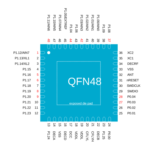
The QFN48 pin assignment figure and table describe the pinouts for this variant of the device.
Pins that can be used as clock signals are shown in as red in the figure. For more information about clock pins, see Clock pins.
| Pin | Clock pin | Name | Function | Description | Dedicated function |
|---|---|---|---|---|---|
| 1 | Yes | P1.12 TRACEDATA[1] AIN7 | Digital I/O Digital I/O Analog input | General purpose IO Trace data Analog input |
Trace
|
| 2 |
| P1.13 TRACEDATA[2] XL1 | Digital I/O Digital I/O Analog input | General purpose IO Trace data Connection for 32.768 kHz crystal |
Trace
|
| 3 |
| P1.14 TRACEDATA[3] XL2 | Digital I/O Digital I/O Analog input | General purpose IO Trace data Connection for 32.768 kHz crystal |
Trace
|
| 4 |
| P1.15 FLPR.4 QSPI.D3 | Digital I/O Digital I/O Digital I/O | General purpose IO General purpose IO QSPI SCK |
FLPR FLPR(QSPI) |
| 5 | Yes | P1.16 FLPR.0 QSPI.SCK | Digital I/O Digital I/O Digital I/O | General purpose IO General purpose IO QSPI D0 |
FLPR FLPR(QSPI) |
| 6 | Yes | P1.17 FLPR.1 QSPI.D1 | Digital I/O Digital I/O Digital I/O | General purpose IO General purpose IO QSPI D1 |
FLPR FLPR(QSPI) |
| 7 |
| P1.18 FLPR.3 QSPI.D2 RADIO[0] | Digital I/O Digital I/O Digital I/O Digital I/O | General purpose IO General purpose IO QSPI D2 RADIO DFEGPIO |
FLPR FLPR(QSPI) RADIO |
| 8 | Yes | P1.19 FLPR.2 QSPI.D1 RADIO[1] | Digital I/O Digital I/O Digital I/O Digital I/O | General purpose IO General purpose IO QSPI D3 RADIO DFEGPIO |
FLPR FLPR(QSPI) RADIO |
| 9 | Yes | P1.20 FLPR.5 QSPI.CSN RADIO[2] | Digital I/O Digital I/O Digital I/O Digital I/O | General purpose IO General purpose IO QSPI CSN RADIO DFEGPIO |
FLPR FLPR(QSPI) RADIO |
| 10 |
| P1.21 FLPR.6 RADIO[3] | Digital I/O Digital I/O Digital I/O | General purpose IO General purpose IO RADIO DFEGPIO |
FLPR RADIO |
| 11 |
| P1.22 FLPR.7 RADIO[4] | Digital I/O Digital I/O Digital I/O | General purpose IO General purpose IO RADIO DFEGPIO |
FLPR RADIO |
| 12 |
| P1.23 FLPR.8 RADIO[5] | Digital I/O Digital I/O Digital I/O | General purpose IO General purpose IO RADIO DFEGPIO |
FLPR RADIO |
| 13 |
| P1.24 FLPR.9 RADIO[6] | Digital I/O Digital I/O Digital I/O | General purpose IO General purpose IO RADIO DFEGPIO |
FLPR RADIO |
| 14 |
| DECA | Power | Power supply decoupling |
|
| 15 |
| VSS | Power | Ground |
|
| 16 |
| DECD | Power | Power supply decoupling |
|
| 17 |
| DCC | Power | DC/DC converter output |
|
| 18 |
| VDDL | Power | Power supply |
|
| 19 |
| CFLYL | Power | Fly capacitor for boost |
|
| 20 |
| VDDL | Power | Power supply |
|
| 21 |
| CFLYH | Power | Fly capacitor for boost |
|
| 22 |
| DECB | Power | Power supply decoupling |
|
| 23 |
| P1.25 | Digital I/O | General purpose IO |
|
| 24 |
| P0.00 | Digital I/O | General purpose IO |
|
| 25 |
| P0.01 | Digital I/O | General purpose IO |
|
| 26 |
| P0.02 | Digital I/O | General purpose IO |
|
| 27 | Yes | P0.03 | Digital I/O Digital I/O | General purpose I/O GRTC PWM |
GRTC |
| 28 | Yes | P0.04 | Digital I/O Digital I/O | General purpose I/O GRTC CLKOUT32K |
GRTC |
| 29 |
| SWDIO | Debug | Serial wire data. Bidirectional with standard-drive and on-chip pull-up. |
|
| 30 |
| SWDCLK | Debug | Serial wire clock. Input with on-chip pull-down. |
|
| 31 |
| nRESET | Reset | Pin reset with on-chip pull-up |
|
| 32 |
| ANT | RF | Single ended radio antenna connection |
|
| 33 |
| VSS | Power | Ground |
|
| 34 |
| DECRF | Power | Power supply decoupling |
|
| 35 |
| XC1 | Analog input | Connection for 32 MHz crystal |
|
| 36 |
| XC2 | Analog input | Connection for 32 MHz crystal |
|
| 37 | Yes | P1.08 | Digital I/O Digital I/O | General purpose I/O GRTC CLKOUTFAST |
GRTC |
| 38 |
| P1.09 | Digital I/O | General purpose I/O |
|
| 39 |
| P1.00 AIN0 | Digital I/O Analog input | General purpose I/O Analog input |
|
| 40 |
| P1.01 AIN1 | Digital I/O Analog input | General purpose I/O Analog input |
|
| 41 |
| P1.02 AIN2 | Digital I/O Analog input | General purpose I/O Analog input |
|
| 42 | Yes | P1.03 AIN3 | Digital I/O Analog input | General purpose I/O Analog input |
|
| 43 |
| P1.06 | Digital I/O | General purpose I/O |
|
| 44 | Yes | P1.04 | Digital I/O | General purpose I/O |
|
| 45 |
| P1.05 ASO[0] EXTREF | Digital I/O Digital I/O Analog input | General purpose IO TAMPC active shield output External reference |
TAMPC |
| 46 |
| P1.07 AIN4 ASI[0] | Digital I/O Analog input Digital I/O | General purpose IO Analog input TAMPC active shield input |
TAMPC |
| 47 |
| P1.10 ASO[1] TRACECLK AIN5 | Digital I/O Digital I/O Digital I/O Analog input | General purpose IO TAMPC active shield output Trace clock Analog input |
TAMPC Trace
|
| 48 | Yes | P1.11 ASI[1] TRACEDATA[0] SWO AIN6 | Digital I/O Digital I/O Digital I/O Digital I/O Analog input | General purpose IO TAMPC active shield input Trace data Serial wire output (SWO) Analog input |
TAMPC Trace
|
| 49 |
| VSS | Power | Ground |
|
Exposed die pad (pin 49) must be connected to ground (VSS, pins 15 and 33) for proper device operation.
CSP29 (CAAA) package pin assignments
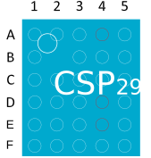
The CSP29 pin assignment figure and table describe the pinouts for this variant of the device.
Pins that can be used as clock signals are shown in as red in the figure. For more information about clock pins, see Clock pins.
| Pin | Clock pin | Name | Function | Description | Dedicated function |
|---|---|---|---|---|---|
| A1 |
| DECRF | Power | Power supply decoupling |
|
| A2 |
| XC1 | Analog input | Connection for 32 MHz crystal |
|
| A3 |
| XC2 | Analog input | Connection for 32 MHz crystal |
|
| A4 | Yes | P1.03 AIN3 | Digital I/O Analog input | General purpose I/O Analog input |
|
| A5 |
| P1.10 ASO[1] TRACECLK AIN5 | Digital I/O Digital I/O Digital I/O Analog input | General purpose IO TAMPC active shield output Trace clock Analog input |
TAMPC Trace
|
| B1 |
| ANT | RF | Single ended radio antenna connection |
|
| B3 |
| P1.09 | Digital I/O | General purpose I/O |
|
| B4 |
| P1.05 ASO[0] EXTREF | Digital I/O Digital I/O Analog input | General purpose IO TAMPC active shield output External reference |
TAMPC |
| B5 |
| P1.13 TRACEDATA[2] XL1 | Digital I/O Digital I/O Analog input | General purpose IO Trace data Connection for 32.768 kHz crystal |
Trace
|
| C1 |
| VSS | Power | Ground |
|
| C2 |
| nRESET | Reset | Pin reset with on-chip pull-up |
|
| C3 |
| P1.01 AIN1 | Digital I/O Analog input | General purpose I/O Analog input |
|
| C4 |
| P1.07 AIN4 ASI[0] | Digital I/O Analog input Digital I/O | General purpose IO Analog input TAMPC active shield input |
TAMPC |
| C5 |
| P1.14 TRACEDATA[3] XL2 | Digital I/O Digital I/O Analog input | General purpose IO Trace data Connection for 32.768 kHz crystal |
Trace
|
| D1 |
| VSS | Power | Ground |
|
| D2 |
| SWDCLK | Debug | Serial wire clock. Input with on-chip pull-down. |
|
| D3 |
| P1.02 AIN2 | Digital I/O Analog input | General purpose I/O Analog input |
|
| D4 | Yes | P1.11 ASI[1] TRACEDATA[0] SWO AIN6 | Digital I/O Digital I/O Digital I/O Digital I/O Analog input | General purpose IO TAMPC active shield input Trace data Serial wire output (SWO) Analog input |
TAMPC Trace
|
| D5 |
| DECA | Power | Power supply decoupling |
|
| E1 |
| DECB | Power | Power supply |
|
| E2 |
| SWDIO | Debug | Serial wire data. Bidirectional with standard-drive and on-chip pull-up. |
|
| E3 |
| P1.00 AIN0 | Digital I/O Analog input | General purpose I/O Analog input |
|
| E4 | Yes | P1.12 TRACEDATA[1] AIN7 | Digital I/O Digital I/O Analog input | General purpose IO Trace data Analog input |
Trace
|
| E5 |
| DECD | Power | Power supply decoupling |
|
| F1 |
| CFLYH | Power | Fly capacitor for boost |
|
| F2 |
| CFLYL | Power | Fly capacitor for boost |
|
| F3 |
| VDDL | Power | Power supply |
|
| F4 |
| VSS | Power | Ground |
|
| F5 |
| DCC | Power | DC/DC converter output |
|