Reference circuitry
To ensure good RF performance when designing PCBs, it is highly recommended to use the PCB layouts and component values provided by Nordic Semiconductor.
Documentation for the different package reference circuits, including Altium Designer files, PCB layout files, and PCB production files can be downloaded from www.nordicsemi.com.
In this section, there are reference circuits for all product variants, showing the components and component values to support on-chip features in a design.
Circuit configuration 1 for CSP29 (CAAA)
In addition to the schematic, the bill of material (BOM) is also provided.
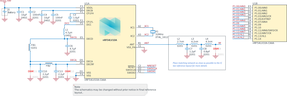
For PCB reference layouts, see the product page for the nRF54LV10A on www.nordicsemi.com.
| Designator | Value | Description | Footprint |
|---|---|---|---|
| C1, C4 | 10 µF | Capacitor, X6S, ±20%, 6.3 V | 0402 |
| C2, C5 | 100 nF | Capacitor, X7R, ±10%, 100 nF, 10 V | 0201 |
| C3 | 1.0 µF | Capacitor, Ceramic, X5R, ±20%, 6.3 V | 0201 |
| C6 | 4.7 µF | Capacitor, Ceramic, X5R, ±20%, 6.3 V | 0201 |
| C7 | 1.2 pF | Capacitor, NP0, ±0.05 pF, 50 V | 0201 |
| C8 | 0.8 pF | Capacitor, NP0, ±0.05 pF, 50 V | 0201 |
| C9 | 0.3 pF | Capacitor, C0G, ±0.1 pF, 50V | 0201 |
| C10, C13 | 2.2 µF | Capacitor, Ceramic, 2.2 µF 2.5V X6T 0201,±20% | 0201 |
| C11 | 10 nF | Capacitor, X7R, 6.3 V | 0201 |
| C12 | 18 pF | Capacitor, C0G, ±5%, 25V | 0201 |
| FB1, FB2 | 120 Ω | Ferrite bead, 120 Ω at 100 MHz, 200 mA, 500 mΩ max | 0201 |
| L1 | 4.7 µH | Inductor, 300 mA, ±20%, 1.08 Ω | 0402 |
| L2 | 2.7 nH | Inductor, 600 mA, ±0.1nH, 120 mΩ | 0201 |
| L3 | 6.2 nH | Inductor, 400 mA, ±3%, 250 mΩ | 0201 |
| L4 | 4.3 nH | Inductor, 500 mA, ±3%, 170 mΩ | 0201 |
| U1 | nRF54LV10A-CAAA | Multiprotocol Bluetooth® Low Energy, IEEE 802.15.4, and 2.4GHz proprietary System on Chip | CSP29 |
| X1 | 32 MHz | XTAL SMD 1612, 32MHz, Cl=8pF, Tot: ±40ppm, Aging: ±1ppm/year | XTAL_1612 |
Circuit configuration 1 for QFN48 (QFAA)
In addition to the schematic, the bill of material (BOM) is also provided.
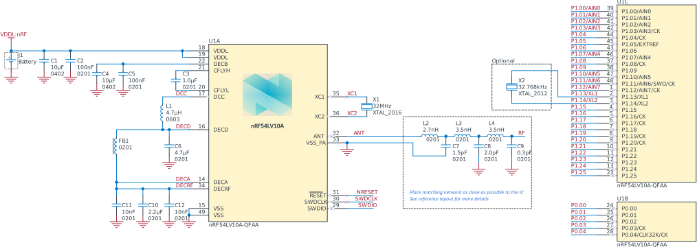
| Designator | Value | Description | Footprint |
|---|---|---|---|
| C1, C4 | 10 µF | Capacitor, X6S, ±20%, 6.3 V | 0402 |
| C2, C5 | 100 nF | Capacitor, X7R, ±10%, 100 nF, 10 V | 0201 |
| C3 | 1.0 µF | Capacitor, Ceramic, X5R, ±20%, 6.3 V | 0201 |
| C6 | 4.7 µF | Capacitor, Ceramic, X5R, ±20%, 6.3 V | 0201 |
| C7 | 1.5 pF | Capacitor, NP0, ±0.05 pF, 25 V | 0201 |
| C8 | 2.0 pF | Capacitor, NP0, ±0.05 pF, 25 V | 0201 |
| C9 | 0.3 pF | Capacitor, C0G, ±0.1pF, 50V | 0201 |
| C10 | 2.2 µF | Capacitor, X6T, ±20%, 2.5V | 0201 |
| C11, C12 | 10 nF | Capacitor, X7R, 6.3 V | 0201 |
| FB1 | 120 Ω | Ferrite bead, 120 Ω at 100 MHz, 200 mA, 500 mΩ max | 0201 |
| L1 | 4.7 µH | Inductor, 120 mA, ±20%, 0.65 Ω | 0603 |
| L2 | 2.7 nH | Inductor, 600 mA, ±0.1nH, 120 mΩ | 0201 |
| L3, L4 | 3.5 nH | Inductor, 500 mA, ±3%, 170 mΩ | 0201 |
| U1 | nRF54LV10A-QFAA | Multiprotocol Bluetooth Low Energy, IEEE 802.15.4, and 2.4GHz proprietary System on Chip | QFN-48 |
| X1 | 32 MHz | XTAL SMD 1612, 32MHz, Cl=8pF, Tot: ±40ppm, Aging: ±1ppm/year | XTAL_1612 |
| X2 | 32.768 kHz | XTAL SMD 2012, 32.768 kHz, 9 pF, ±20 ppm | XTAL_2012 |
PCB layout example
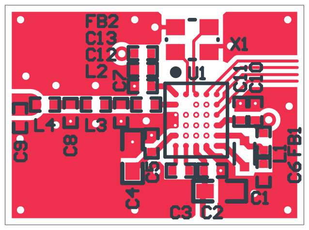
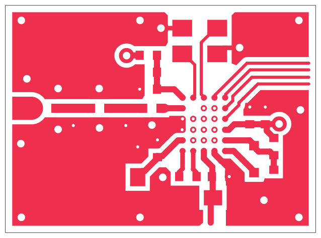
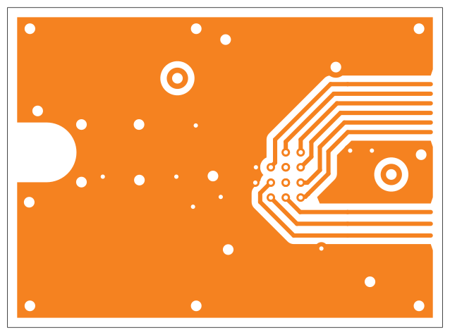
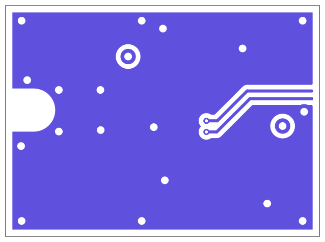
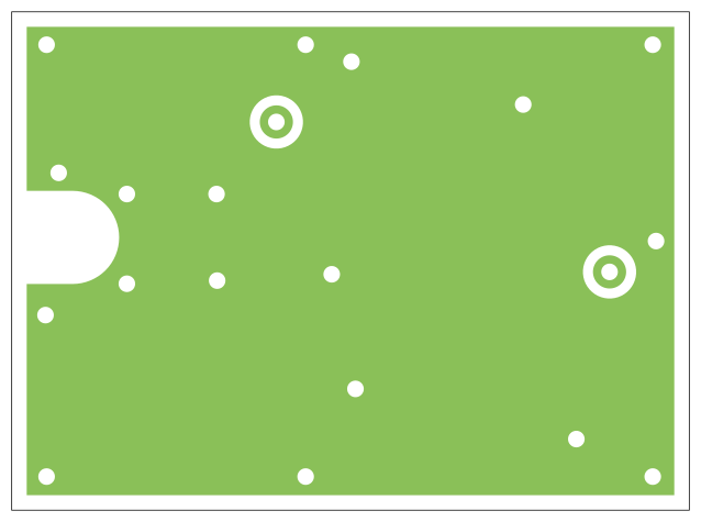
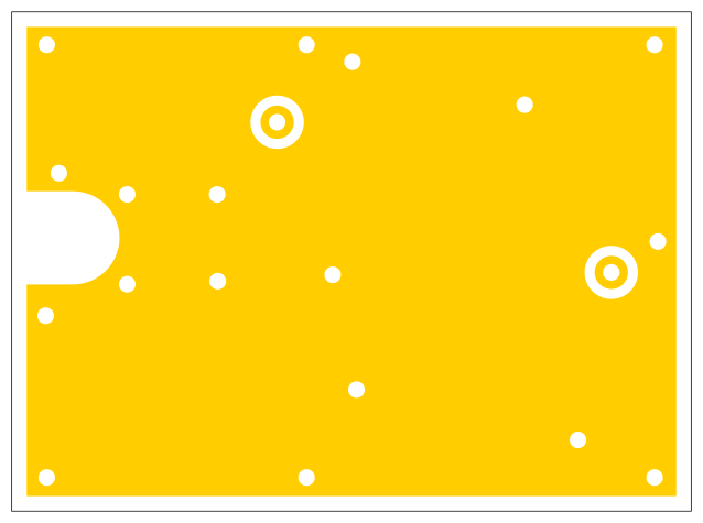
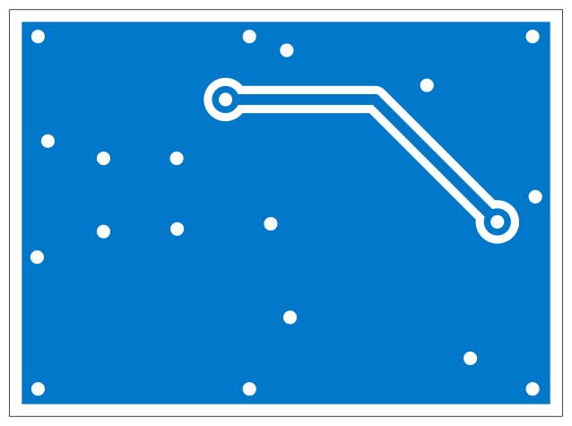
The PCB layout in the following figure is a reference layout for Circuit configuration 1 for CSP29 (CAAA).
For all available reference layouts, see the product page for nRF54LV10A on www.nordicsemi.com.