Pin assignments
This section describes the pin assignment and the pin functions of the nRF9151.
The device provides flexibility when it comes to routing and configuration of the GPIO pins. However, for some pins there are recommendations on pin usage and configuration. See following table for more information about this.
LGA pin assignments
The pin assignment table and figure describe the assignments.
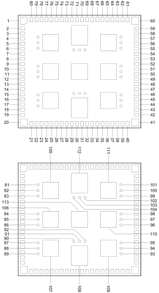
| Pin no | Pin name | Function | Description |
|---|---|---|---|
| 1 | GND | Power | Ground |
| 2 | P0.20 AIN7 | Digital I/O (SoC) Analog input | General purpose I/O. Analog input. |
| 3 | SWDCLK | Digital input | Serial wire debug clock input for debug and programming |
| 4 | SWDIO | Digital I/O | Serial wire debug I/O for debug and programming |
| 5 | P0.21 TRACECLK | Digital I/O (SoC) Trace clock | General purpose I/O. Trace buffer clock (optional). |
| 6 | P0.22 TRACEDATA[0] | Digital I/O (SoC) Trace data | General purpose I/O. Trace buffer TRACEDATA[0] (optional). |
| 7 | GND | Power | Ground |
| 8 | P0.23 TRACEDATA[1] | Digital I/O (SoC) Trace data | General purpose I/O. Trace buffer TRACEDATA[1] (optional). |
| 9 | nRESET | Digital I/O (SoC) | SoC reset pin1,2 |
| 10 | ENABLE | Enable for the SiP internal regulator for the nRF91 SoC. Note: The nRF9151 will not start until this pin
is enabled. | |
| 11 | P0.24 TRACEDATA[2] | Digital I/O (SoC) Trace data | General purpose I/O. Trace buffer TRACEDATA[2] (optional). |
| 12 | P0.25 TRACEDATA[3] | Digital I/O (SoC) Trace data | General purpose I/O. Trace buffer TRACEDATA[3] (optional). |
| 13 | GND | Power | Ground |
| 14 | VDD | Power | Supply voltage |
| 15 | GND | Power | Ground |
| 16 | SIM_RST | Digital I/O (SoC) | SIM reset |
| 17 | SIM_IO | Digital I/O (SoC) | SIM data |
| 18 | SIM_CLK | Digital I/O (SoC) | SIM clock |
| 19 | SIM_1V8 | Power | SIM 1.8 V power supply output |
| 20 | GND | Power | Ground |
| 21 | MAGPIO0 | Digital I/O (SoC) | 1.8 V general purpose I/O |
| 22 | MAGPIO1 | Digital I/O (SoC) | 1.8 V general purpose I/O |
| 23 | MAGPIO2 | Digital I/O (SoC) | 1.8 V general purpose I/O |
| 24 | DEC0 | Power | Power supply decoupling. Reserved for Nordic use. |
| 25 | GND | Power | Ground |
| 26 | SIM_DET | Digital I/O (SoC) | SIM detect Not used. Must be left floating. |
| 27 | SDATA | Digital I/O (SoC) | MIPI RFFE control interface |
| 28 | SCLK | Digital I/O (SoC) | MIPI RFFE control interface |
| 29 | VIO | Power | MIPI RFFE control interface |
| 30 | GND | Power | Ground |
| 31 | RESERVED | Connect thermally and mechanically to the application board but leave electrically unconnected. | |
| 32 | RESERVED | Connect thermally and mechanically to the application board but leave electrically unconnected. | |
| 33 | RESERVED | Connect thermally and mechanically to the application board but leave electrically unconnected. | |
| 34 | GND | Power | Ground |
| 35 | ANT | RF | Single-ended 50 Ω LTE antenna pin |
| 36 | GND | Power | Ground |
| 37 | AUX | RF | Single-ended 50 Ω ANT loop-back pin |
| 38 | GND | Power | Ground |
| 39 | GND | Power | Ground |
| 40 | GND | Power | Ground |
| 41 | GND | Power | Ground |
| 42 | GPS | RF | Single-ended 50 Ω GPS input pin |
| 43 | GND | Power | Ground |
| 44 | P0.26 | Digital I/O (SoC) | General purpose I/O |
| 45 | P0.27 | Digital I/O (SoC) | General purpose I/O |
| 46 | GND | Power | Ground |
| 47 | P0.28 | Digital I/O (SoC) | General purpose I/O |
| 48 | P0.29 | Digital I/O (SoC) | General purpose I/O |
| 49 | P0.30 | Digital I/O (SoC) | General purpose I/O |
| 50 | P0.31 | Digital I/O (SoC) | General purpose I/O |
| 51 | GND | Power | Ground |
| 52 | COEX0 | Digital I/O (SoC) | Coexistence interface |
| 53 | COEX1 | Digital I/O (SoC) | Coexistence interface |
| 54 | COEX2 | Digital I/O (SoC) | Coexistence interface |
| 55 | GND | Power | Ground |
| 56 | P0.00 | Digital I/O (SoC) | General purpose I/O |
| 57 | P0.01 | Digital I/O (SoC) | General purpose I/O |
| 58 | P0.02 | Digital I/O (SoC) | General purpose I/O |
| 59 | P0.03 | Digital I/O (SoC) | General purpose I/O |
| 60 | GND | Power | Ground |
| 61 | P0.04 | Digital I/O (SoC) | General purpose I/O |
| 62 | P0.05 | Digital I/O (SoC) | General purpose I/O |
| 63 | P0.06 | Digital I/O (SoC) | General purpose I/O |
| 64 | P0.07 | Digital I/O (SoC) | General purpose I/O |
| 65 | VDD_GPIO | Power | GPIO power supply input and logic level |
| 66 | GND | Power | Ground |
| 67 | P0.08 | Digital I/O (SoC) | General purpose I/O |
| 68 | P0.09 | Digital I/O (SoC) | General purpose I/O |
| 69 | P0.10 | Digital I/O (SoC) | General purpose I/O |
| 70 | P0.11 | Digital I/O (SoC) | General purpose I/O |
| 71 | GND | Power | Ground |
| 72 | P0.12 | Digital I/O (SoC) | General purpose I/O |
| 73 | P0.13 AIN0 | Digital I/O (SoC) Analog input | General purpose I/O. Analog input. |
| 74 | P0.14 AIN1 | Digital I/O (SoC) Analog input | General purpose I/O. Analog input. |
| 75 | P0.15 AIN2 | Digital I/O (SoC) Analog input | General purpose I/O. Analog input. |
| 76 | GND | Power | Ground |
| 77 | P0.16 AIN3 | Digital I/O (SoC) Analog input | General purpose I/O. Analog input. |
| 78 | P0.17 AIN4 | Digital I/O (SoC) Analog input | General purpose I/O. Analog input. |
| 79 | P0.18 AIN5 | Digital I/O (SoC) Analog input | General purpose I/O. Analog input. |
| 80 | P0.19 AIN6 | Digital I/O (SoC) Analog input | General purpose I/O. Analog input. |
| 81 | RESERVED | Do not connect/reserved for future use | |
| 82 | RESERVED | Do not connect/reserved for future use | |
| 83 | RESERVED | Do not connect/reserved for future use | |
| 84 | RESERVED | Do not connect/reserved for future use | |
| 85 | RESERVED | Do not connect/reserved for future use | |
| 86 | RESERVED | Do not connect/reserved for future use | |
| 87 | RESERVED | Do not connect/reserved for future use | |
| 88 | RESERVED | Do not connect/reserved for future use | |
| 89 | RESERVED | Do not connect/reserved for future use | |
| 90 | RESERVED | Do not connect/reserved for future use | |
| 91 | RESERVED | Do not connect/reserved for future use | |
| 92 | RESERVED | Do not connect/reserved for future use | |
| 93 | RESERVED | Do not connect/reserved for future use | |
| 94 | RESERVED | Do not connect/reserved for future use | |
| 95 | RESERVED | Do not connect/reserved for future use | |
| 96 | RESERVED | Do not connect/reserved for future use | |
| 97 | RESERVED | Do not connect/reserved for future use | |
| 98 | RESERVED | Do not connect/reserved for future use | |
| 99 | RESERVED | Do not connect/reserved for future use | |
| 100 | RESERVED | Do not connect/reserved for future use | |
| 101 | RESERVED | Do not connect/reserved for future use | |
| 102 | RESERVED | Do not connect/reserved for future use | |
| 103 | RESERVED | Do not connect/reserved for future use | |
| 104 | RESERVED | Do not connect/reserved for future use | |
| 105 | GND | Power | Ground |
| 106 | GND | Power | Ground |
| 107 | GND | Power | Ground |
| 108 | GND | Power | Ground |
| 109 | GND | Power | Ground |
| 110 | GND | Power | Ground |
| 111 | GND | Power | Ground |
| 112 | GND | Power | Ground |
| 113 | GND | Power | Ground |