IPC — Interprocessor communication
The interprocessor communication (IPC) peripheral is used to send and receive events between MCUs in the system.
Functional description
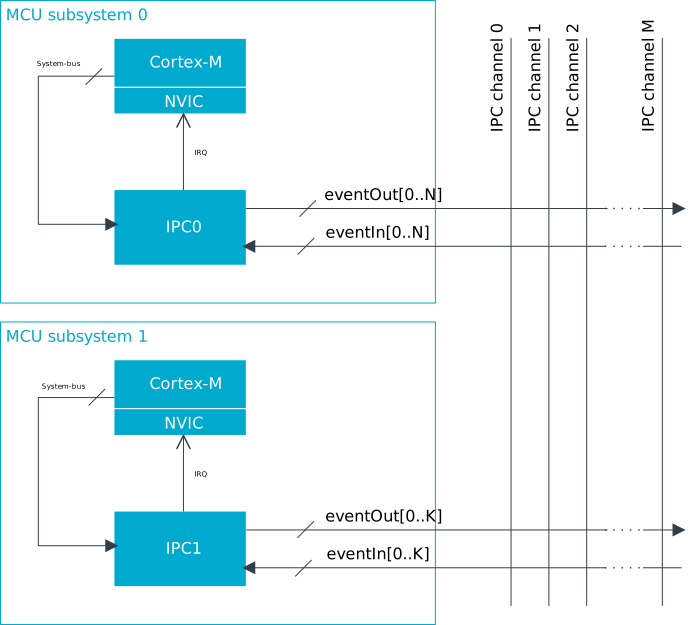
IPC block diagram illustrates the interprocessor communication (IPC) peripheral. In a multi-MCU system, each MCU has one dedicated IPC peripheral. The IPC peripheral can be used to send and receive events to and from other IPC peripherals. An instance of the IPC peripheral can have multiple SEND tasks and RECEIVE events. A single SEND task can be configured to signal an event on one or more IPC channels, and a RECEIVE event can be configured to listen on one or more IPC channels. The IPC channels that are triggered in a SEND task can be configured through the SEND_CNF registers, and the IPC channels that trigger a RECEIVE event are configured through the RECEIVE_CNF registers. The figure below illustrates how the SEND_CNF and RECEIVE_CNF registers work. Both the SEND task and the RECEIVE event can be connected to all IPC channels.
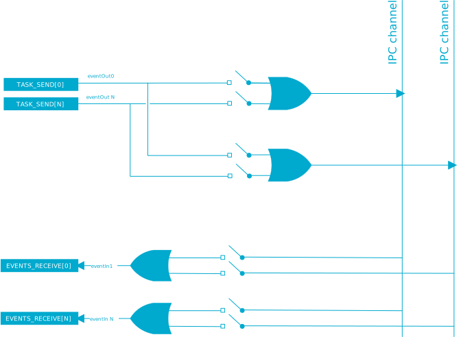
A SEND task can be viewed as broadcasting events onto one or more IPC channels, and a RECEIVE event can be seen as subscribing to a subset of IPC channels. It is possible for multiple IPCs to trigger events onto the same channel at the same time. When two or more events on the same channel occur within tIPC, the events may be merged into a single event seen from the IPC receiver. One of the events can therefore be lost. To prevent this, the user must ensure that events on the same IPC channel do not occur within tIPC of each other. When implementing firmware data structures, such as queues or mailboxes, this can be done by using one channel for acknowledgements.
An IPC event often does not contain any data itself, it is used to signal other MCUs that something has occurred. Data can be shared through shared memory, for example in the form of a software implemented mailbox, or command/event queues. It is up to software to assign a logical functionality to an IPC channel. For instance, one IPC channel can be used to signal that a command is ready to be executed, and any processor in the system can subscribe to that particular channel and decode/execute the command.
General purpose memory
The GPMEM registers can be used freely to store information. These registers are accessed like any other of the IPC peripheral's registers.
IPC and PPI connections
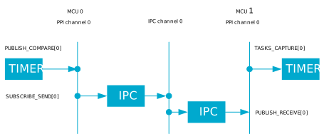
The IPC SEND tasks and RECEIVE events can be connected through PPI channels. This makes it possible to relay events from peripherals in one MCU to another, without CPU involvement.
Figure below illustrates a timer COMPARE event that is relayed from one MCU to IPC using PPI, then back into a timer CAPTURE event in another MCU.
Registers
Instances
| Instance | Base address | TrustZone | Split access | Description | ||
|---|---|---|---|---|---|---|
| Map | Att | DMA | ||||
IPC : S | 0x5002A000 | US | NS | NA | No | Interprocessor communication |
Register overview
| Register | Offset | TZ | Description |
|---|---|---|---|
| TASKS_SEND[n] | 0x000 | Trigger events on IPC channel enabled in SEND_CNF[n] | |
| SUBSCRIBE_SEND[n] | 0x080 | Subscribe configuration for task SEND[n] | |
| EVENTS_RECEIVE[n] | 0x100 | Event received on one or more of the enabled IPC channels in RECEIVE_CNF[n] | |
| PUBLISH_RECEIVE[n] | 0x180 | Publish configuration for event RECEIVE[n] | |
| INTEN | 0x300 | Enable or disable interrupt | |
| INTENSET | 0x304 | Enable interrupt | |
| INTENCLR | 0x308 | Disable interrupt | |
| INTPEND | 0x30C | Pending interrupts | |
| SEND_CNF[n] | 0x510 | Send event configuration for TASKS_SEND[n] | |
| RECEIVE_CNF[n] | 0x590 | Receive event configuration for EVENTS_RECEIVE[n] | |
| GPMEM[n] | 0x610 | General purpose memory |
TASKS_SEND[n] (n=0..7)
Address offset: 0x000 + (n × 0x4)
Trigger events on IPC channel enabled in SEND_CNF[n]
| Bit number | 31 | 30 | 29 | 28 | 27 | 26 | 25 | 24 | 23 | 22 | 21 | 20 | 19 | 18 | 17 | 16 | 15 | 14 | 13 | 12 | 11 | 10 | 9 | 8 | 7 | 6 | 5 | 4 | 3 | 2 | 1 | 0 | |||
|---|---|---|---|---|---|---|---|---|---|---|---|---|---|---|---|---|---|---|---|---|---|---|---|---|---|---|---|---|---|---|---|---|---|---|---|
| ID | A | ||||||||||||||||||||||||||||||||||
| Reset 0x00000000 | 0 | 0 | 0 | 0 | 0 | 0 | 0 | 0 | 0 | 0 | 0 | 0 | 0 | 0 | 0 | 0 | 0 | 0 | 0 | 0 | 0 | 0 | 0 | 0 | 0 | 0 | 0 | 0 | 0 | 0 | 0 | 0 | |||
| ID | R/W | Field | Value ID | Value | Description | ||||||||||||||||||||||||||||||
| A | W | TASKS_SEND | Trigger events on IPC channel enabled in SEND_CNF[n] | ||||||||||||||||||||||||||||||||
Trigger | 1 | Trigger task | |||||||||||||||||||||||||||||||||
SUBSCRIBE_SEND[n] (n=0..7)
Address offset: 0x080 + (n × 0x4)
Subscribe configuration for task SEND[n]
| Bit number | 31 | 30 | 29 | 28 | 27 | 26 | 25 | 24 | 23 | 22 | 21 | 20 | 19 | 18 | 17 | 16 | 15 | 14 | 13 | 12 | 11 | 10 | 9 | 8 | 7 | 6 | 5 | 4 | 3 | 2 | 1 | 0 | |||
|---|---|---|---|---|---|---|---|---|---|---|---|---|---|---|---|---|---|---|---|---|---|---|---|---|---|---|---|---|---|---|---|---|---|---|---|
| ID | B | A | A | A | A | A | A | A | A | ||||||||||||||||||||||||||
| Reset 0x00000000 | 0 | 0 | 0 | 0 | 0 | 0 | 0 | 0 | 0 | 0 | 0 | 0 | 0 | 0 | 0 | 0 | 0 | 0 | 0 | 0 | 0 | 0 | 0 | 0 | 0 | 0 | 0 | 0 | 0 | 0 | 0 | 0 | |||
| ID | R/W | Field | Value ID | Value | Description | ||||||||||||||||||||||||||||||
| A | RW | CHIDX | [0..255] | DPPI channel that task SEND[n] will subscribe to | |||||||||||||||||||||||||||||||
| B | RW | EN | |||||||||||||||||||||||||||||||||
Disabled | 0 | Disable subscription | |||||||||||||||||||||||||||||||||
Enabled | 1 | Enable subscription | |||||||||||||||||||||||||||||||||
EVENTS_RECEIVE[n] (n=0..7)
Address offset: 0x100 + (n × 0x4)
Event received on one or more of the enabled IPC channels in RECEIVE_CNF[n]
| Bit number | 31 | 30 | 29 | 28 | 27 | 26 | 25 | 24 | 23 | 22 | 21 | 20 | 19 | 18 | 17 | 16 | 15 | 14 | 13 | 12 | 11 | 10 | 9 | 8 | 7 | 6 | 5 | 4 | 3 | 2 | 1 | 0 | |||
|---|---|---|---|---|---|---|---|---|---|---|---|---|---|---|---|---|---|---|---|---|---|---|---|---|---|---|---|---|---|---|---|---|---|---|---|
| ID | A | ||||||||||||||||||||||||||||||||||
| Reset 0x00000000 | 0 | 0 | 0 | 0 | 0 | 0 | 0 | 0 | 0 | 0 | 0 | 0 | 0 | 0 | 0 | 0 | 0 | 0 | 0 | 0 | 0 | 0 | 0 | 0 | 0 | 0 | 0 | 0 | 0 | 0 | 0 | 0 | |||
| ID | R/W | Field | Value ID | Value | Description | ||||||||||||||||||||||||||||||
| A | RW | EVENTS_RECEIVE | Event received on one or more of the enabled IPC channels in RECEIVE_CNF[n] | ||||||||||||||||||||||||||||||||
NotGenerated | 0 | Event not generated | |||||||||||||||||||||||||||||||||
Generated | 1 | Event generated | |||||||||||||||||||||||||||||||||
PUBLISH_RECEIVE[n] (n=0..7)
Address offset: 0x180 + (n × 0x4)
Publish configuration for event RECEIVE[n]
| Bit number | 31 | 30 | 29 | 28 | 27 | 26 | 25 | 24 | 23 | 22 | 21 | 20 | 19 | 18 | 17 | 16 | 15 | 14 | 13 | 12 | 11 | 10 | 9 | 8 | 7 | 6 | 5 | 4 | 3 | 2 | 1 | 0 | |||
|---|---|---|---|---|---|---|---|---|---|---|---|---|---|---|---|---|---|---|---|---|---|---|---|---|---|---|---|---|---|---|---|---|---|---|---|
| ID | B | A | A | A | A | A | A | A | A | ||||||||||||||||||||||||||
| Reset 0x00000000 | 0 | 0 | 0 | 0 | 0 | 0 | 0 | 0 | 0 | 0 | 0 | 0 | 0 | 0 | 0 | 0 | 0 | 0 | 0 | 0 | 0 | 0 | 0 | 0 | 0 | 0 | 0 | 0 | 0 | 0 | 0 | 0 | |||
| ID | R/W | Field | Value ID | Value | Description | ||||||||||||||||||||||||||||||
| A | RW | CHIDX | [0..255] | DPPI channel that event RECEIVE[n] will publish to | |||||||||||||||||||||||||||||||
| B | RW | EN | |||||||||||||||||||||||||||||||||
Disabled | 0 | Disable publishing | |||||||||||||||||||||||||||||||||
Enabled | 1 | Enable publishing | |||||||||||||||||||||||||||||||||
INTEN
Address offset: 0x300
Enable or disable interrupt
| Bit number | 31 | 30 | 29 | 28 | 27 | 26 | 25 | 24 | 23 | 22 | 21 | 20 | 19 | 18 | 17 | 16 | 15 | 14 | 13 | 12 | 11 | 10 | 9 | 8 | 7 | 6 | 5 | 4 | 3 | 2 | 1 | 0 | |||
|---|---|---|---|---|---|---|---|---|---|---|---|---|---|---|---|---|---|---|---|---|---|---|---|---|---|---|---|---|---|---|---|---|---|---|---|
| ID | H | G | F | E | D | C | B | A | |||||||||||||||||||||||||||
| Reset 0x00000000 | 0 | 0 | 0 | 0 | 0 | 0 | 0 | 0 | 0 | 0 | 0 | 0 | 0 | 0 | 0 | 0 | 0 | 0 | 0 | 0 | 0 | 0 | 0 | 0 | 0 | 0 | 0 | 0 | 0 | 0 | 0 | 0 | |||
| ID | R/W | Field | Value ID | Value | Description | ||||||||||||||||||||||||||||||
| A-H | RW | RECEIVE[i] (i=0..7) | Enable or disable interrupt for event RECEIVE[i] | ||||||||||||||||||||||||||||||||
Disabled | 0 | Disable | |||||||||||||||||||||||||||||||||
Enabled | 1 | Enable | |||||||||||||||||||||||||||||||||
INTENSET
Address offset: 0x304
Enable interrupt
| Bit number | 31 | 30 | 29 | 28 | 27 | 26 | 25 | 24 | 23 | 22 | 21 | 20 | 19 | 18 | 17 | 16 | 15 | 14 | 13 | 12 | 11 | 10 | 9 | 8 | 7 | 6 | 5 | 4 | 3 | 2 | 1 | 0 | |||
|---|---|---|---|---|---|---|---|---|---|---|---|---|---|---|---|---|---|---|---|---|---|---|---|---|---|---|---|---|---|---|---|---|---|---|---|
| ID | H | G | F | E | D | C | B | A | |||||||||||||||||||||||||||
| Reset 0x00000000 | 0 | 0 | 0 | 0 | 0 | 0 | 0 | 0 | 0 | 0 | 0 | 0 | 0 | 0 | 0 | 0 | 0 | 0 | 0 | 0 | 0 | 0 | 0 | 0 | 0 | 0 | 0 | 0 | 0 | 0 | 0 | 0 | |||
| ID | R/W | Field | Value ID | Value | Description | ||||||||||||||||||||||||||||||
| A-H | RW | RECEIVE[i] (i=0..7) | Write '1' to enable interrupt for event RECEIVE[i] | ||||||||||||||||||||||||||||||||
Set | 1 | Enable | |||||||||||||||||||||||||||||||||
Disabled | 0 | Read: Disabled | |||||||||||||||||||||||||||||||||
Enabled | 1 | Read: Enabled | |||||||||||||||||||||||||||||||||
INTENCLR
Address offset: 0x308
Disable interrupt
| Bit number | 31 | 30 | 29 | 28 | 27 | 26 | 25 | 24 | 23 | 22 | 21 | 20 | 19 | 18 | 17 | 16 | 15 | 14 | 13 | 12 | 11 | 10 | 9 | 8 | 7 | 6 | 5 | 4 | 3 | 2 | 1 | 0 | |||
|---|---|---|---|---|---|---|---|---|---|---|---|---|---|---|---|---|---|---|---|---|---|---|---|---|---|---|---|---|---|---|---|---|---|---|---|
| ID | H | G | F | E | D | C | B | A | |||||||||||||||||||||||||||
| Reset 0x00000000 | 0 | 0 | 0 | 0 | 0 | 0 | 0 | 0 | 0 | 0 | 0 | 0 | 0 | 0 | 0 | 0 | 0 | 0 | 0 | 0 | 0 | 0 | 0 | 0 | 0 | 0 | 0 | 0 | 0 | 0 | 0 | 0 | |||
| ID | R/W | Field | Value ID | Value | Description | ||||||||||||||||||||||||||||||
| A-H | RW | RECEIVE[i] (i=0..7) | Write '1' to disable interrupt for event RECEIVE[i] | ||||||||||||||||||||||||||||||||
Clear | 1 | Disable | |||||||||||||||||||||||||||||||||
Disabled | 0 | Read: Disabled | |||||||||||||||||||||||||||||||||
Enabled | 1 | Read: Enabled | |||||||||||||||||||||||||||||||||
INTPEND
Address offset: 0x30C
Pending interrupts
| Bit number | 31 | 30 | 29 | 28 | 27 | 26 | 25 | 24 | 23 | 22 | 21 | 20 | 19 | 18 | 17 | 16 | 15 | 14 | 13 | 12 | 11 | 10 | 9 | 8 | 7 | 6 | 5 | 4 | 3 | 2 | 1 | 0 | |||
|---|---|---|---|---|---|---|---|---|---|---|---|---|---|---|---|---|---|---|---|---|---|---|---|---|---|---|---|---|---|---|---|---|---|---|---|
| ID | H | G | F | E | D | C | B | A | |||||||||||||||||||||||||||
| Reset 0x00000000 | 0 | 0 | 0 | 0 | 0 | 0 | 0 | 0 | 0 | 0 | 0 | 0 | 0 | 0 | 0 | 0 | 0 | 0 | 0 | 0 | 0 | 0 | 0 | 0 | 0 | 0 | 0 | 0 | 0 | 0 | 0 | 0 | |||
| ID | R/W | Field | Value ID | Value | Description | ||||||||||||||||||||||||||||||
| A-H | R | RECEIVE[i] (i=0..7) | Read pending status of interrupt for event RECEIVE[i] | ||||||||||||||||||||||||||||||||
NotPending | 0 | Read: Not pending | |||||||||||||||||||||||||||||||||
Pending | 1 | Read: Pending | |||||||||||||||||||||||||||||||||
SEND_CNF[n] (n=0..7)
Address offset: 0x510 + (n × 0x4)
Send event configuration for TASKS_SEND[n]
| Bit number | 31 | 30 | 29 | 28 | 27 | 26 | 25 | 24 | 23 | 22 | 21 | 20 | 19 | 18 | 17 | 16 | 15 | 14 | 13 | 12 | 11 | 10 | 9 | 8 | 7 | 6 | 5 | 4 | 3 | 2 | 1 | 0 | |||
|---|---|---|---|---|---|---|---|---|---|---|---|---|---|---|---|---|---|---|---|---|---|---|---|---|---|---|---|---|---|---|---|---|---|---|---|
| ID | H | G | F | E | D | C | B | A | |||||||||||||||||||||||||||
| Reset 0x00000000 | 0 | 0 | 0 | 0 | 0 | 0 | 0 | 0 | 0 | 0 | 0 | 0 | 0 | 0 | 0 | 0 | 0 | 0 | 0 | 0 | 0 | 0 | 0 | 0 | 0 | 0 | 0 | 0 | 0 | 0 | 0 | 0 | |||
| ID | R/W | Field | Value ID | Value | Description | ||||||||||||||||||||||||||||||
| A-H | RW | CHEN[i] (i=0..7) | Enable broadcasting on IPC channel i | ||||||||||||||||||||||||||||||||
Disable | 0 | Disable broadcast | |||||||||||||||||||||||||||||||||
Enable | 1 | Enable broadcast | |||||||||||||||||||||||||||||||||
RECEIVE_CNF[n] (n=0..7)
Address offset: 0x590 + (n × 0x4)
Receive event configuration for EVENTS_RECEIVE[n]
| Bit number | 31 | 30 | 29 | 28 | 27 | 26 | 25 | 24 | 23 | 22 | 21 | 20 | 19 | 18 | 17 | 16 | 15 | 14 | 13 | 12 | 11 | 10 | 9 | 8 | 7 | 6 | 5 | 4 | 3 | 2 | 1 | 0 | |||
|---|---|---|---|---|---|---|---|---|---|---|---|---|---|---|---|---|---|---|---|---|---|---|---|---|---|---|---|---|---|---|---|---|---|---|---|
| ID | H | G | F | E | D | C | B | A | |||||||||||||||||||||||||||
| Reset 0x00000000 | 0 | 0 | 0 | 0 | 0 | 0 | 0 | 0 | 0 | 0 | 0 | 0 | 0 | 0 | 0 | 0 | 0 | 0 | 0 | 0 | 0 | 0 | 0 | 0 | 0 | 0 | 0 | 0 | 0 | 0 | 0 | 0 | |||
| ID | R/W | Field | Value ID | Value | Description | ||||||||||||||||||||||||||||||
| A-H | RW | CHEN[i] (i=0..7) | Enable subscription to IPC channel i | ||||||||||||||||||||||||||||||||
Disable | 0 | Disable events | |||||||||||||||||||||||||||||||||
Enable | 1 | Enable events | |||||||||||||||||||||||||||||||||
GPMEM[n] (n=0..3)
Address offset: 0x610 + (n × 0x4)
General purpose memory
Retained only in System ON mode
| Bit number | 31 | 30 | 29 | 28 | 27 | 26 | 25 | 24 | 23 | 22 | 21 | 20 | 19 | 18 | 17 | 16 | 15 | 14 | 13 | 12 | 11 | 10 | 9 | 8 | 7 | 6 | 5 | 4 | 3 | 2 | 1 | 0 | |||
|---|---|---|---|---|---|---|---|---|---|---|---|---|---|---|---|---|---|---|---|---|---|---|---|---|---|---|---|---|---|---|---|---|---|---|---|
| ID | A | A | A | A | A | A | A | A | A | A | A | A | A | A | A | A | A | A | A | A | A | A | A | A | A | A | A | A | A | A | A | A | |||
| Reset 0x00000000 | 0 | 0 | 0 | 0 | 0 | 0 | 0 | 0 | 0 | 0 | 0 | 0 | 0 | 0 | 0 | 0 | 0 | 0 | 0 | 0 | 0 | 0 | 0 | 0 | 0 | 0 | 0 | 0 | 0 | 0 | 0 | 0 | |||
| ID | R/W | Field | Value ID | Value | Description | ||||||||||||||||||||||||||||||
| A | RW | GPMEM | General purpose memory | ||||||||||||||||||||||||||||||||
Electrical specification
IPC Electrical Specification
| Symbol | Description | Min. | Typ. | Max. | Units |
|---|---|---|---|---|---|
| tIPC | Time window during which IPC events can be merged | 165 | µs |