Debug and trace
The debug and trace system offers a flexible and powerful mechanism for non-intrusive debugging.
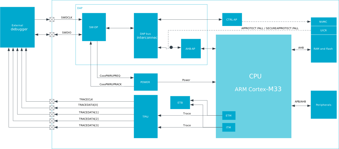
- Two-pin serial wire debug (SWD) interface, protocol version 1
- Access port connection
- Breakpoint unit (BPU) supports eight hardware breakpoint comparators
- Data watchpoint and trace (DWT) unit supports four watchpoint comparators
- Instrumentation trace macrocell (ITM)
- Embedded trace macrocell (ETM)
- Access protection through APPROTECT, ERASEPROTECT and SECUREAPPROTECT
- Embedded trace buffer (ETB)
- Trace port interface unit (TPIU)
- 4-bit parallel trace of ITM and ETM trace data
Special consideration regarding debugger access
A debugger, if desired, can be restricted to debug non-secure code only, and access non-secure memory regions and peripherals using register SECUREAPPROTECT. Register APPROTECT will block all debugger access.
| Debugging capability | UICR.APPROTECT.PALL | UICR.SECUREAPPROTECT.PALL |
|---|---|---|
| Secure and non-secure code | Unprotected | Unprotected |
| Non-secure code only | Unprotected | Protected |
| No debugging possible | Protected | - |
If a RAM or flash region has its permission set to allow code execution, the content of this region will be visible to the debugger even if the read permission is not set. This allows a debugger to display the content of the code being executed. For more about how to configure permissions, please refer to SPU — System protection unit.
DAP - Debug access port
An external debugger can access the device via the debug access port (DAP).
The DAP implements a standard Arm® CoreSight™ serial wire debug port (SW-DP). The SW-DP implements the serial wire debug (SWD) protocol that is a two-pin serial interface, see SWDCLK and SWDIO illustrated in figure Debug and trace overview.
In addition to the default access port in the application CPU (AHB-AP), the DAP includes a custom control access port (CTRL-AP), described in more detail in CTRL-AP - Control access port.
- The SWDIO line has an internal pull-up resistor.
- The SWDCLK line has an internal pull-down resistor.
There are several access ports that connect to different parts of the system. An overview is given in the table below.
| AP ID | Type | Description |
|---|---|---|
| 0 | AHB-AP | Application subsystem access port |
| 3 | APB-AP | CoreSight™ subsystem access port |
| 4 | CTRL-AP | Application subsystem control access port |
The standard Arm® components are documented in Arm CoreSight SoC-400 Technical Reference Manual, revision r3p2. The control access port (CTRL-AP) is proprietary, and described in more detail in CTRL-AP - Control access port.
Debug interface mode
Before the external debugger can access the CPU's access port (AHB-AP) or the control access port (CTRL-AP), the debugger must first request the device to power up via CxxxPWRUPREQ in the SWJ-DP.
As long as the debugger is requesting power via CxxxPWRUPREQ, the device will be in debug interface mode. Otherwise, the device is in normal mode. When a debug session is over, the external debugger must make sure to put the device back into normal mode and then a pin reset should be performed. The reason is that the overall power consumption is higher in debug interface mode compared to normal mode.
Some peripherals behave differently in debug interface mode compared to normal mode. The differences are described in more detail in the chapters of the affected peripherals.
For details on how to use the debug capabilities, please read the debug documentation of your IDE.
If the device is in System OFF when power is requested via CxxxPWRUPREQ, the system will wake up and the DIF flag in RESETREAS will be set.
Real-time debug
The device supports real-time debugging, which allows interrupts to execute to completion in real time when breakpoints are set in thread mode or lower priority interrupts.
Real-time debugging thus enables the developer to set a breakpoint and single-step through their code without a failure of the real-time event-driven threads running at higher priority. For example, this enables the device to continue to service the high-priority interrupts of an external controller or sensor without failure or loss of state synchronization while the developer steps through code in a low-priority thread.
Registers
Register overview
| Register | Offset | Description |
|---|---|---|
| TARGETID | 0x042 | The TARGETID register provides information about the target when the host is connected to a single device. The TARGETID register is accessed by a read of DP register 0x4 when the DPBANKSEL bit in the SELECT register is set to 0x2. |
TARGETID
Address offset: 0x042
The TARGETID register provides information about the target when the host is connected to a single device.
The TARGETID register is accessed by a read of DP register 0x4 when the DPBANKSEL bit in the SELECT register is set to 0x2.
| Bit number | 31 | 30 | 29 | 28 | 27 | 26 | 25 | 24 | 23 | 22 | 21 | 20 | 19 | 18 | 17 | 16 | 15 | 14 | 13 | 12 | 11 | 10 | 9 | 8 | 7 | 6 | 5 | 4 | 3 | 2 | 1 | 0 | |||
|---|---|---|---|---|---|---|---|---|---|---|---|---|---|---|---|---|---|---|---|---|---|---|---|---|---|---|---|---|---|---|---|---|---|---|---|
| ID | D | D | D | D | C | C | C | C | C | C | C | C | C | C | C | C | B | B | B | B | B | B | B | B | B | B | B | A | |||||||
| Reset 0x10090289 | 0 | 0 | 0 | 1 | 0 | 0 | 0 | 0 | 0 | 0 | 0 | 0 | 1 | 0 | 0 | 1 | 0 | 0 | 0 | 0 | 0 | 0 | 1 | 0 | 1 | 0 | 0 | 0 | 1 | 0 | 0 | 1 | |||
| ID | R/W | Field | Value ID | Value | Description | ||||||||||||||||||||||||||||||
| A | R | UNUSED | Reserved, read-as-one | ||||||||||||||||||||||||||||||||
| B | R | TDESIGNER | An 11-bit code: JEDEC JEP106 continuation code and identity code. The ID identifies the designer of the part. | ||||||||||||||||||||||||||||||||
NordicSemi | 0x144 | Nordic Semiconductor ASA | |||||||||||||||||||||||||||||||||
| C | R | TPARTNO | Part number | ||||||||||||||||||||||||||||||||
| D | R | TREVISION | Target revision | ||||||||||||||||||||||||||||||||
Electrical specification
Trace port
| Symbol | Description | Min. | Typ. | Max. | Units |
|---|---|---|---|---|---|
| Tcyc | Clock period, as defined by ARM (See ARM Infocenter, Embedded Trace Macrocell Architecture Specification, Trace Port Physical Interface, Timing specifications) | 62.5 | ns |