Reference circuitry
To ensure good RF performance when designing PCBs, using the PCB layouts and component values provided by Nordic Semiconductor is highly recommended .
Documentation for the different package reference circuits, including Altium Designer files, PCB layout files, and PCB production files can be downloaded from the product page at www.nordicsemi.com.
In this section, there are reference circuits for SIxA to show the components and component values to support on-chip features in a design.
Note: This is not a complete list of configurations, but all required circuitry is shown for
further configurations.
Schematic SIxA LGA127
Circuit configuration for SIxA LGA127, showing the schematic and the Bill of Materials (BOM) table.
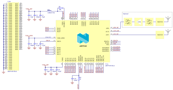
| Designator | Value | Description | Footprint |
|---|---|---|---|
| C1, C7 | 15 pF | Capacitor, NP0, ±0.1pF, 25 V | 0201 |
| C2, C4, C8, C10 | 100 nF | Capacitor, X5R, ±10% | 0201 |
| C3, C9 | 47 μF | Capacitor, X5R, ±20%, 10 V | 0805 |
| C5 | 4.7 µF | Capacitor, X5R, ±20% | 0402 |
| C6 | 4.7 µF | Capacitor, X5R, ±10%, 16 V | 0805 |
| R1 | 10 kΩ | Resistor, ±1%, 0.05 W | 0201 |
| R2 | 1 k | Resistor, ±1%, 0.05 W | 0201 |
| FB1 | 120 R / 0.70 A | Ferrite Bead, 120 Ω @ 100 MHz, 700 mA, 130 mΩ Max | 0402 |
| U1 | nRF9160-SIxA | Low power System-in-Package (SiP) with integrated LTE-M/NB-IoT modem and GPS | LGA |
For PCB reference layouts, see the product page for the nRF9160 at www.nordicsemi.com.