Trace
The nRF9161 supports ETM and ITM trace.
Available trace sinks:
- 2 kB internal embedded trace buffer (ETB)
- External trace port interface through TPIU
Trace data from the ETM and the ITM can be sent to an internal embedded trace buffer (ETB) or an external debugger via a 4-bit wide parallel trace port (TPIU), see TRACEDATA[0] through TRACEDATA[3], and TRACECLK in Debug and trace overview.
The following diagram shows the trace components architecture of the device's embedded Arm® CoreSight™ subsystem.
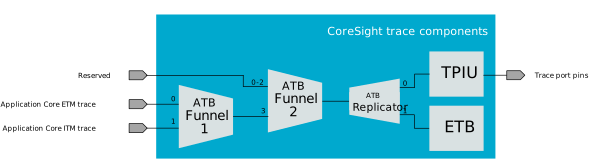
The standard Arm® components are documented in Arm CoreSight SoC-400 Technical Reference Manual, revision r3p2. For details on how to use the trace capabilities, please read the debug documentation of your IDE.
TPIU's trace pins are multiplexed with GPIOs, see Pin assignments for more information.
Trace speed is configured in the TRACEPORTSPEED (Retained) register. The speed of the trace pins depends on the DRIVE setting of the GPIOs that the trace pins are multiplexed with. See GPIO — General purpose input/output for information about how to set drive settings. Only S0S1 and H0H1 drives are suitable for debugging. S0S1 is the default DRIVE at reset. If parallel or serial trace port signals are not fast enough in the debugging conditions, all GPIOs in use for tracing should be set to high drive (H0H1). The user shall make sure that DRIVE setting for these GPIOs is not overwritten by software during the debugging session.
ATB Funnel
The ARM® ATB Funnel funnels trace bus mesages from several sources into one output bus.
This document only provides a register-level description of this ARM component. See the ARM® CoreSight™ SoC-400 Technical Reference Manual for more details
Registers
Instances
| Instance | Base address | TrustZone | Split access | Description | ||
|---|---|---|---|---|---|---|
| Map | Att | DMA | ||||
| ATBFUNNEL1 | 0xE005A000 | HF | NS | NA | No | ATBFUNNEL unit 1 |
| ATBFUNNEL2 | 0xE005B000 | HF | NS | NA | No | ATBFUNNEL unit 2 |
Register overview
| Register | Offset | TZ | Description |
|---|---|---|---|
| CTRLREG | 0x000 | The IDFILTER0 register enables the programming of ID filtering for master port 0. | |
| PRIORITYCTRLREG | 0x004 | The Priority_Ctrl_Reg register defines the order in which inputs are selected. Each 3-bit field is a priority for each particular slave interface. | |
| ITATBDATA0 | 0xEEC | The ITATBDATA0 register performs different functions depending on whether the access is a read or a write. | |
| ITATBCTR2 | 0xEF0 | The ITATBCTR2 register performs different functions depending on whether the access is a read or a write. | |
| ITATBCTR1 | 0xEF4 | The ITATBCTR1 register performs different functions depending on whether the access is a read or a write. | |
| ITATBCTR0 | 0xEF8 | The ITATBCTR0 register performs different functions depending on whether the access is a read or a write. | |
| ITCTRL | 0xF00 | The ITCTRL register enables the component to switch from a functional mode, which is the default behavior, to integration mode where the inputs and outputs of the component can be directly controlled for the purposes of integration testing and topology detection. | |
| CLAIMSET | 0xFA0 | Software can use the claim tag to coordinate application and debugger access to trace unit functionality. The claim tags have no effect on the operation of the component. The CLAIMSET register sets bits in the claim tag, and determines the number of claim bits implemented. | |
| CLAIMCLR | 0xFA4 | Software can use the claim tag to coordinate application and debugger access to trace unit functionality. The claim tags have no effect on the operation of the component. The CLAIMCLR register sets the bits in the claim tag to 0 and determines the current value of the claim tag. | |
| LAR | 0xFB0 | This is used to enable write access to device registers. | |
| LSR | 0xFB4 | This indicates the status of the lock control mechanism. This lock prevents accidental writes by code under debug. Accesses to the extended stimulus port registers are not affected by the lock mechanism. This register must always be present although there might not be any lock access control mechanism. The lock mechanism, where present and locked, must block write accesses to any control register, except the Lock Access Register. For most components this covers all registers except for the Lock Access Register. | |
| AUTHSTATUS | 0xFB8 | Indicates the current level of tracing permitted by the system | |
| DEVID | 0xFC8 | Indicates the capabilities of the component. | |
| DEVTYPE | 0xFCC | The DEVTYPE register provides a debugger with information about the component when the Part Number field is not recognized. The debugger can then report this information. | |
| PIDR4 | 0xFD0 | Coresight peripheral identification registers. | |
| PIDR[0] | 0xFE0 | Coresight peripheral identification registers. | |
| PIDR[1] | 0xFE4 | Coresight peripheral identification registers. | |
| PIDR[2] | 0xFE8 | Coresight peripheral identification registers. | |
| PIDR[3] | 0xFEC | Coresight peripheral identification registers. | |
| CIDR[0] | 0xFF0 | Coresight component identification registers. | |
| CIDR[1] | 0xFF4 | Coresight component identification registers. | |
| CIDR[2] | 0xFF8 | Coresight component identification registers. | |
| CIDR[3] | 0xFFC | Coresight component identification registers. |
CTRLREG
Address offset: 0x000
The IDFILTER0 register enables the programming of ID filtering for master port 0.
| Bit number | 31 | 30 | 29 | 28 | 27 | 26 | 25 | 24 | 23 | 22 | 21 | 20 | 19 | 18 | 17 | 16 | 15 | 14 | 13 | 12 | 11 | 10 | 9 | 8 | 7 | 6 | 5 | 4 | 3 | 2 | 1 | 0 | |||
|---|---|---|---|---|---|---|---|---|---|---|---|---|---|---|---|---|---|---|---|---|---|---|---|---|---|---|---|---|---|---|---|---|---|---|---|
| ID | I | I | I | I | H | G | F | E | D | C | B | A | |||||||||||||||||||||||
| Reset 0x00000000 | 0 | 0 | 0 | 0 | 0 | 0 | 0 | 0 | 0 | 0 | 0 | 0 | 0 | 0 | 0 | 0 | 0 | 0 | 0 | 0 | 0 | 0 | 0 | 0 | 0 | 0 | 0 | 0 | 0 | 0 | 0 | 0 | |||
| ID | R/W | Field | Value ID | Value | Description | ||||||||||||||||||||||||||||||
| A-H | RW | ENS[i] (i=0..7) | Enable slave port i. | ||||||||||||||||||||||||||||||||
Disabled | 0 | Slave port disabled. This excludes the port from the priority selection scheme. | |||||||||||||||||||||||||||||||||
Enabled | 1 | Slave port enabled. | |||||||||||||||||||||||||||||||||
| I | RW | HT | [0:14] | Hold Time. The formatting scheme can become inefficient when fast switching occurs, and you can use this setting to minimize switching. When a source has nothing to transmit, then another source is selected irrespective of the minimum number of transactions. The ATB funnel holds for the minimum hold time and one additional transaction. The actual hold time is the register value plus 1. The maximum value that can be entered is 0b1110 and this equates to 15 transactions. 0b1111 is reserved. | |||||||||||||||||||||||||||||||
PRIORITYCTRLREG
Address offset: 0x004
The Priority_Ctrl_Reg register defines the order in which inputs are selected. Each 3-bit field is a priority for each particular slave interface.
| Bit number | 31 | 30 | 29 | 28 | 27 | 26 | 25 | 24 | 23 | 22 | 21 | 20 | 19 | 18 | 17 | 16 | 15 | 14 | 13 | 12 | 11 | 10 | 9 | 8 | 7 | 6 | 5 | 4 | 3 | 2 | 1 | 0 | |||
|---|---|---|---|---|---|---|---|---|---|---|---|---|---|---|---|---|---|---|---|---|---|---|---|---|---|---|---|---|---|---|---|---|---|---|---|
| ID | H | H | H | G | G | G | F | F | F | E | E | E | D | D | D | C | C | C | B | B | B | A | A | A | |||||||||||
| Reset 0x00000000 | 0 | 0 | 0 | 0 | 0 | 0 | 0 | 0 | 0 | 0 | 0 | 0 | 0 | 0 | 0 | 0 | 0 | 0 | 0 | 0 | 0 | 0 | 0 | 0 | 0 | 0 | 0 | 0 | 0 | 0 | 0 | 0 | |||
| ID | R/W | Field | Value ID | Value | Description | ||||||||||||||||||||||||||||||
| A-H | RW | PRIPORT[i] (i=0..7) | [0:7] | Priority value of port number i. | |||||||||||||||||||||||||||||||
ITATBDATA0
Address offset: 0xEEC
The ITATBDATA0 register performs different functions depending on whether the access is a read or a write.
| Bit number | 31 | 30 | 29 | 28 | 27 | 26 | 25 | 24 | 23 | 22 | 21 | 20 | 19 | 18 | 17 | 16 | 15 | 14 | 13 | 12 | 11 | 10 | 9 | 8 | 7 | 6 | 5 | 4 | 3 | 2 | 1 | 0 | |||
|---|---|---|---|---|---|---|---|---|---|---|---|---|---|---|---|---|---|---|---|---|---|---|---|---|---|---|---|---|---|---|---|---|---|---|---|
| ID | Q | P | O | N | M | L | K | J | I | H | G | F | E | D | C | B | A | ||||||||||||||||||
| Reset 0x00000000 | 0 | 0 | 0 | 0 | 0 | 0 | 0 | 0 | 0 | 0 | 0 | 0 | 0 | 0 | 0 | 0 | 0 | 0 | 0 | 0 | 0 | 0 | 0 | 0 | 0 | 0 | 0 | 0 | 0 | 0 | 0 | 0 | |||
| ID | R/W | Field | Value ID | Value | Description | ||||||||||||||||||||||||||||||
| A-Q | RW | ATDATA[i] (i=0..16) | A read access returns the value of a pin on atdatas_x of the enabled port. A write access writes to the corresponding atdatam pin of the enabled port. | ||||||||||||||||||||||||||||||||
Low | 0 | Pin is logic 0. | |||||||||||||||||||||||||||||||||
High | 1 | Pin is logic 1. | |||||||||||||||||||||||||||||||||
ITATBCTR2
Address offset: 0xEF0
The ITATBCTR2 register performs different functions depending on whether the access is a read or a write.
| Bit number | 31 | 30 | 29 | 28 | 27 | 26 | 25 | 24 | 23 | 22 | 21 | 20 | 19 | 18 | 17 | 16 | 15 | 14 | 13 | 12 | 11 | 10 | 9 | 8 | 7 | 6 | 5 | 4 | 3 | 2 | 1 | 0 | |||
|---|---|---|---|---|---|---|---|---|---|---|---|---|---|---|---|---|---|---|---|---|---|---|---|---|---|---|---|---|---|---|---|---|---|---|---|
| ID | B | A | |||||||||||||||||||||||||||||||||
| Reset 0x00000000 | 0 | 0 | 0 | 0 | 0 | 0 | 0 | 0 | 0 | 0 | 0 | 0 | 0 | 0 | 0 | 0 | 0 | 0 | 0 | 0 | 0 | 0 | 0 | 0 | 0 | 0 | 0 | 0 | 0 | 0 | 0 | 0 | |||
| ID | R/W | Field | Value ID | Value | Description | ||||||||||||||||||||||||||||||
| A | RW | ATREADY | A read access returns the value of atreadym. A write access outputs the data to afvalids[n], where the value of the CTRLREG at 0x000 defines n. | ||||||||||||||||||||||||||||||||
Low | 0 | Pin is logic 0. | |||||||||||||||||||||||||||||||||
High | 1 | Pin is logic 1. | |||||||||||||||||||||||||||||||||
| B | RW | AFVALID | A read access returns the value of afvalidm. A write access outputs the data to atreadys[n], where the value of the CTRLREG at 0x000 defines n. | ||||||||||||||||||||||||||||||||
Low | 0 | Pin is logic 0. | |||||||||||||||||||||||||||||||||
High | 1 | Pin is logic 1. | |||||||||||||||||||||||||||||||||
ITATBCTR1
Address offset: 0xEF4
The ITATBCTR1 register performs different functions depending on whether the access is a read or a write.
| Bit number | 31 | 30 | 29 | 28 | 27 | 26 | 25 | 24 | 23 | 22 | 21 | 20 | 19 | 18 | 17 | 16 | 15 | 14 | 13 | 12 | 11 | 10 | 9 | 8 | 7 | 6 | 5 | 4 | 3 | 2 | 1 | 0 | |||
|---|---|---|---|---|---|---|---|---|---|---|---|---|---|---|---|---|---|---|---|---|---|---|---|---|---|---|---|---|---|---|---|---|---|---|---|
| ID | A | A | A | A | A | A | A | ||||||||||||||||||||||||||||
| Reset 0x00000000 | 0 | 0 | 0 | 0 | 0 | 0 | 0 | 0 | 0 | 0 | 0 | 0 | 0 | 0 | 0 | 0 | 0 | 0 | 0 | 0 | 0 | 0 | 0 | 0 | 0 | 0 | 0 | 0 | 0 | 0 | 0 | 0 | |||
| ID | R/W | Field | Value ID | Value | Description | ||||||||||||||||||||||||||||||
| A | RW | ATVALIDM0 | A read returns the value of the atids[n] signals, where the value of the Control Register at 0x000 defines n. A write outputs the value to the atidm port. | ||||||||||||||||||||||||||||||||
Low | 0 | Pin is logic 0. | |||||||||||||||||||||||||||||||||
High | 1 | Pin is logic 1. | |||||||||||||||||||||||||||||||||
ITATBCTR0
Address offset: 0xEF8
The ITATBCTR0 register performs different functions depending on whether the access is a read or a write.
| Bit number | 31 | 30 | 29 | 28 | 27 | 26 | 25 | 24 | 23 | 22 | 21 | 20 | 19 | 18 | 17 | 16 | 15 | 14 | 13 | 12 | 11 | 10 | 9 | 8 | 7 | 6 | 5 | 4 | 3 | 2 | 1 | 0 | |||
|---|---|---|---|---|---|---|---|---|---|---|---|---|---|---|---|---|---|---|---|---|---|---|---|---|---|---|---|---|---|---|---|---|---|---|---|
| ID | C | C | B | A | |||||||||||||||||||||||||||||||
| Reset 0x00000000 | 0 | 0 | 0 | 0 | 0 | 0 | 0 | 0 | 0 | 0 | 0 | 0 | 0 | 0 | 0 | 0 | 0 | 0 | 0 | 0 | 0 | 0 | 0 | 0 | 0 | 0 | 0 | 0 | 0 | 0 | 0 | 0 | |||
| ID | R/W | Field | Value ID | Value | Description | ||||||||||||||||||||||||||||||
| A | RW | ATVALID | A read returns the value of the atvalids[n] signal, where the value of the CTRLREG at 0x000 defines n. A write outputs the value to atvalidm. | ||||||||||||||||||||||||||||||||
Low | 0 | Pin is logic 0. | |||||||||||||||||||||||||||||||||
High | 1 | Pin is logic 1. | |||||||||||||||||||||||||||||||||
| B | RW | AFREADY | A read returns the value of the afreadys[n] signal, where the value of the Ctrl_Reg at 0x000 defines n. A write outputs the value to afreadym. | ||||||||||||||||||||||||||||||||
Low | 0 | Pin is logic 0. | |||||||||||||||||||||||||||||||||
High | 1 | Pin is logic 1. | |||||||||||||||||||||||||||||||||
| C | RW | ATBYTES | A read returns the value of the atbytess[n] signal, where the value of the Ctrl_Reg at 0x000 defines n. A write outputs the value to atbytesm. | ||||||||||||||||||||||||||||||||
Low | 0 | Pin is logic 0. | |||||||||||||||||||||||||||||||||
High | 1 | Pin is logic 1. | |||||||||||||||||||||||||||||||||
ITCTRL
Address offset: 0xF00
The ITCTRL register enables the component to switch from a functional mode, which is the default behavior, to integration mode where the inputs and outputs of the component can be directly controlled for the purposes of integration testing and topology detection.
| Bit number | 31 | 30 | 29 | 28 | 27 | 26 | 25 | 24 | 23 | 22 | 21 | 20 | 19 | 18 | 17 | 16 | 15 | 14 | 13 | 12 | 11 | 10 | 9 | 8 | 7 | 6 | 5 | 4 | 3 | 2 | 1 | 0 | |||
|---|---|---|---|---|---|---|---|---|---|---|---|---|---|---|---|---|---|---|---|---|---|---|---|---|---|---|---|---|---|---|---|---|---|---|---|
| ID | A | ||||||||||||||||||||||||||||||||||
| Reset 0x00000000 | 0 | 0 | 0 | 0 | 0 | 0 | 0 | 0 | 0 | 0 | 0 | 0 | 0 | 0 | 0 | 0 | 0 | 0 | 0 | 0 | 0 | 0 | 0 | 0 | 0 | 0 | 0 | 0 | 0 | 0 | 0 | 0 | |||
| ID | R/W | Field | Value ID | Value | Description | ||||||||||||||||||||||||||||||
| A | RW | IME | Integration Mode Enable. | ||||||||||||||||||||||||||||||||
Disabled | 0 | Integration mode disabled. | |||||||||||||||||||||||||||||||||
Enabled | 1 | Integration mode enabled. | |||||||||||||||||||||||||||||||||
CLAIMSET
Address offset: 0xFA0
Software can use the claim tag to coordinate application and debugger access to trace unit functionality. The claim tags have no effect on the operation of the component. The CLAIMSET register sets bits in the claim tag, and determines the number of claim bits implemented.
| Bit number | 31 | 30 | 29 | 28 | 27 | 26 | 25 | 24 | 23 | 22 | 21 | 20 | 19 | 18 | 17 | 16 | 15 | 14 | 13 | 12 | 11 | 10 | 9 | 8 | 7 | 6 | 5 | 4 | 3 | 2 | 1 | 0 | |||
|---|---|---|---|---|---|---|---|---|---|---|---|---|---|---|---|---|---|---|---|---|---|---|---|---|---|---|---|---|---|---|---|---|---|---|---|
| ID | D | C | B | A | |||||||||||||||||||||||||||||||
| Reset 0x00000000 | 0 | 0 | 0 | 0 | 0 | 0 | 0 | 0 | 0 | 0 | 0 | 0 | 0 | 0 | 0 | 0 | 0 | 0 | 0 | 0 | 0 | 0 | 0 | 0 | 0 | 0 | 0 | 0 | 0 | 0 | 0 | 0 | |||
| ID | R/W | Field | Value ID | Value | Description | ||||||||||||||||||||||||||||||
| A-D | RW | BIT[i] (i=0..3) | Set claim bit i and check if bit is implemented or not. | ||||||||||||||||||||||||||||||||
NotImplemented | 0 | Claim bit i is not implemented. | |||||||||||||||||||||||||||||||||
Implemented | 1 | Claim bit i is implemented. | |||||||||||||||||||||||||||||||||
Set | 1 | Set claim bit i. | |||||||||||||||||||||||||||||||||
CLAIMCLR
Address offset: 0xFA4
Software can use the claim tag to coordinate application and debugger access to trace unit functionality. The claim tags have no effect on the operation of the component. The CLAIMCLR register sets the bits in the claim tag to 0 and determines the current value of the claim tag.
| Bit number | 31 | 30 | 29 | 28 | 27 | 26 | 25 | 24 | 23 | 22 | 21 | 20 | 19 | 18 | 17 | 16 | 15 | 14 | 13 | 12 | 11 | 10 | 9 | 8 | 7 | 6 | 5 | 4 | 3 | 2 | 1 | 0 | |||
|---|---|---|---|---|---|---|---|---|---|---|---|---|---|---|---|---|---|---|---|---|---|---|---|---|---|---|---|---|---|---|---|---|---|---|---|
| ID | D | C | B | A | |||||||||||||||||||||||||||||||
| Reset 0x00000000 | 0 | 0 | 0 | 0 | 0 | 0 | 0 | 0 | 0 | 0 | 0 | 0 | 0 | 0 | 0 | 0 | 0 | 0 | 0 | 0 | 0 | 0 | 0 | 0 | 0 | 0 | 0 | 0 | 0 | 0 | 0 | 0 | |||
| ID | R/W | Field | Value ID | Value | Description | ||||||||||||||||||||||||||||||
| A-D | RW | BIT[i] (i=0..3) | Read or clear claim bit i. | ||||||||||||||||||||||||||||||||
Cleared | 0 | Claim bit i is not set. | |||||||||||||||||||||||||||||||||
Set | 1 | Claim bit i is set. | |||||||||||||||||||||||||||||||||
Clear | 1 | Clear claim bit i. | |||||||||||||||||||||||||||||||||
LAR
Address offset: 0xFB0
This is used to enable write access to device registers.
| Bit number | 31 | 30 | 29 | 28 | 27 | 26 | 25 | 24 | 23 | 22 | 21 | 20 | 19 | 18 | 17 | 16 | 15 | 14 | 13 | 12 | 11 | 10 | 9 | 8 | 7 | 6 | 5 | 4 | 3 | 2 | 1 | 0 | |||
|---|---|---|---|---|---|---|---|---|---|---|---|---|---|---|---|---|---|---|---|---|---|---|---|---|---|---|---|---|---|---|---|---|---|---|---|
| ID | A | A | A | A | A | A | A | A | A | A | A | A | A | A | A | A | A | A | A | A | A | A | A | A | A | A | A | A | A | A | A | A | |||
| Reset 0x00000000 | 0 | 0 | 0 | 0 | 0 | 0 | 0 | 0 | 0 | 0 | 0 | 0 | 0 | 0 | 0 | 0 | 0 | 0 | 0 | 0 | 0 | 0 | 0 | 0 | 0 | 0 | 0 | 0 | 0 | 0 | 0 | 0 | |||
| ID | R/W | Field | Value ID | Value | Description | ||||||||||||||||||||||||||||||
| A | RW | ACCESS | A write of 0xC5ACCE55 enables further write access to this device. Any other write removes write access. | ||||||||||||||||||||||||||||||||
UnLock | 0xC5ACCE55 | Unlock register interface. | |||||||||||||||||||||||||||||||||
LSR
Address offset: 0xFB4
This indicates the status of the lock control mechanism. This lock prevents accidental writes by code under debug. Accesses to the extended stimulus port registers are not affected by the lock mechanism. This register must always be present although there might not be any lock access control mechanism. The lock mechanism, where present and locked, must block write accesses to any control register, except the Lock Access Register. For most components this covers all registers except for the Lock Access Register.
| Bit number | 31 | 30 | 29 | 28 | 27 | 26 | 25 | 24 | 23 | 22 | 21 | 20 | 19 | 18 | 17 | 16 | 15 | 14 | 13 | 12 | 11 | 10 | 9 | 8 | 7 | 6 | 5 | 4 | 3 | 2 | 1 | 0 | |||
|---|---|---|---|---|---|---|---|---|---|---|---|---|---|---|---|---|---|---|---|---|---|---|---|---|---|---|---|---|---|---|---|---|---|---|---|
| ID | C | B | A | ||||||||||||||||||||||||||||||||
| Reset 0x00000000 | 0 | 0 | 0 | 0 | 0 | 0 | 0 | 0 | 0 | 0 | 0 | 0 | 0 | 0 | 0 | 0 | 0 | 0 | 0 | 0 | 0 | 0 | 0 | 0 | 0 | 0 | 0 | 0 | 0 | 0 | 0 | 0 | |||
| ID | R/W | Field | Value ID | Value | Description | ||||||||||||||||||||||||||||||
| A | RW | PRESENT | Indicates that a lock control mechanism exists for this device. | ||||||||||||||||||||||||||||||||
NotImplemented | 0 | No lock control mechanism exists, writes to the Lock Access Register are ignored. | |||||||||||||||||||||||||||||||||
Implemented | 1 | Lock control mechanism is present. | |||||||||||||||||||||||||||||||||
| B | RW | LOCKED | Returns the current status of the Lock. | ||||||||||||||||||||||||||||||||
UnLocked | 0 | Write access is allowed to this device. | |||||||||||||||||||||||||||||||||
Locked | 1 | Write access to the component is blocked. All writes to control registers are ignored. Reads are permitted. | |||||||||||||||||||||||||||||||||
| C | RW | TYPE | Indicates if the Lock Access Register is implemented as 8-bit or 32-bit. | ||||||||||||||||||||||||||||||||
Bits32 | 0 | This component implements a 32-bit Lock Access Register. | |||||||||||||||||||||||||||||||||
Bits8 | 1 | This component implements an 8-bit Lock Access Register. | |||||||||||||||||||||||||||||||||
AUTHSTATUS
Address offset: 0xFB8
Indicates the current level of tracing permitted by the system
| Bit number | 31 | 30 | 29 | 28 | 27 | 26 | 25 | 24 | 23 | 22 | 21 | 20 | 19 | 18 | 17 | 16 | 15 | 14 | 13 | 12 | 11 | 10 | 9 | 8 | 7 | 6 | 5 | 4 | 3 | 2 | 1 | 0 | |||
|---|---|---|---|---|---|---|---|---|---|---|---|---|---|---|---|---|---|---|---|---|---|---|---|---|---|---|---|---|---|---|---|---|---|---|---|
| ID | D | D | C | C | B | B | A | A | |||||||||||||||||||||||||||
| Reset 0x00000000 | 0 | 0 | 0 | 0 | 0 | 0 | 0 | 0 | 0 | 0 | 0 | 0 | 0 | 0 | 0 | 0 | 0 | 0 | 0 | 0 | 0 | 0 | 0 | 0 | 0 | 0 | 0 | 0 | 0 | 0 | 0 | 0 | |||
| ID | R/W | Field | Value ID | Value | Description | ||||||||||||||||||||||||||||||
| A | RW | NSID | Non-secure Invasive Debug | ||||||||||||||||||||||||||||||||
NotImplemented | 0 | The feature is not implemented. | |||||||||||||||||||||||||||||||||
Implemented | 1 | The feature is implemented. | |||||||||||||||||||||||||||||||||
| B | RW | NSNID | Non-secure Non-Invasive Debug | ||||||||||||||||||||||||||||||||
NotImplemented | 0 | The feature is not implemented. | |||||||||||||||||||||||||||||||||
Implemented | 1 | The feature is implemented. | |||||||||||||||||||||||||||||||||
| C | RW | SID | Secure Invasive Debug | ||||||||||||||||||||||||||||||||
NotImplemented | 0 | The feature is not implemented. | |||||||||||||||||||||||||||||||||
Implemented | 1 | The feature is implemented. | |||||||||||||||||||||||||||||||||
| D | RW | SNID | Secure Non-Invasive Debug | ||||||||||||||||||||||||||||||||
NotImplemented | 0 | The feature is not implemented. | |||||||||||||||||||||||||||||||||
Implemented | 1 | The feature is implemented. | |||||||||||||||||||||||||||||||||
DEVID
Address offset: 0xFC8
Indicates the capabilities of the component.
| Bit number | 31 | 30 | 29 | 28 | 27 | 26 | 25 | 24 | 23 | 22 | 21 | 20 | 19 | 18 | 17 | 16 | 15 | 14 | 13 | 12 | 11 | 10 | 9 | 8 | 7 | 6 | 5 | 4 | 3 | 2 | 1 | 0 | |||
|---|---|---|---|---|---|---|---|---|---|---|---|---|---|---|---|---|---|---|---|---|---|---|---|---|---|---|---|---|---|---|---|---|---|---|---|
| ID | A | A | A | A | |||||||||||||||||||||||||||||||
| Reset 0x00000000 | 0 | 0 | 0 | 0 | 0 | 0 | 0 | 0 | 0 | 0 | 0 | 0 | 0 | 0 | 0 | 0 | 0 | 0 | 0 | 0 | 0 | 0 | 0 | 0 | 0 | 0 | 0 | 0 | 0 | 0 | 0 | 0 | |||
| ID | R/W | Field | Value ID | Value | Description | ||||||||||||||||||||||||||||||
| A | R | PORTCOUNT | [2:8] | Indicates the number of input ports connected. 0x0 and 0x1 are illegal values. | |||||||||||||||||||||||||||||||
DEVTYPE
Address offset: 0xFCC
The DEVTYPE register provides a debugger with information about the component when the Part Number field is not recognized. The debugger can then report this information.
| Bit number | 31 | 30 | 29 | 28 | 27 | 26 | 25 | 24 | 23 | 22 | 21 | 20 | 19 | 18 | 17 | 16 | 15 | 14 | 13 | 12 | 11 | 10 | 9 | 8 | 7 | 6 | 5 | 4 | 3 | 2 | 1 | 0 | |||
|---|---|---|---|---|---|---|---|---|---|---|---|---|---|---|---|---|---|---|---|---|---|---|---|---|---|---|---|---|---|---|---|---|---|---|---|
| ID | B | B | B | B | A | A | A | A | |||||||||||||||||||||||||||
| Reset 0x00000000 | 0 | 0 | 0 | 0 | 0 | 0 | 0 | 0 | 0 | 0 | 0 | 0 | 0 | 0 | 0 | 0 | 0 | 0 | 0 | 0 | 0 | 0 | 0 | 0 | 0 | 0 | 0 | 0 | 0 | 0 | 0 | 0 | |||
| ID | R/W | Field | Value ID | Value | Description | ||||||||||||||||||||||||||||||
| A | R | MAJOR | The main type of the component | ||||||||||||||||||||||||||||||||
InputOutputDevice | 2 | Indicates that this component has ATB inputs and outputs. | |||||||||||||||||||||||||||||||||
| B | R | SUB | The sub-type of the component | ||||||||||||||||||||||||||||||||
Replicator | 1 | This component arbitrates ATB inputs mapping to ATB outputs. | |||||||||||||||||||||||||||||||||
PIDR4
Address offset: 0xFD0
Coresight peripheral identification registers.
| Bit number | 31 | 30 | 29 | 28 | 27 | 26 | 25 | 24 | 23 | 22 | 21 | 20 | 19 | 18 | 17 | 16 | 15 | 14 | 13 | 12 | 11 | 10 | 9 | 8 | 7 | 6 | 5 | 4 | 3 | 2 | 1 | 0 | |||
|---|---|---|---|---|---|---|---|---|---|---|---|---|---|---|---|---|---|---|---|---|---|---|---|---|---|---|---|---|---|---|---|---|---|---|---|
| ID | |||||||||||||||||||||||||||||||||||
| Reset 0x00000000 | 0 | 0 | 0 | 0 | 0 | 0 | 0 | 0 | 0 | 0 | 0 | 0 | 0 | 0 | 0 | 0 | 0 | 0 | 0 | 0 | 0 | 0 | 0 | 0 | 0 | 0 | 0 | 0 | 0 | 0 | 0 | 0 | |||
| ID | R/W | Field | Value ID | Value | Description | ||||||||||||||||||||||||||||||
PIDR[0]
Address offset: 0xFE0
Coresight peripheral identification registers.
| Bit number | 31 | 30 | 29 | 28 | 27 | 26 | 25 | 24 | 23 | 22 | 21 | 20 | 19 | 18 | 17 | 16 | 15 | 14 | 13 | 12 | 11 | 10 | 9 | 8 | 7 | 6 | 5 | 4 | 3 | 2 | 1 | 0 | |||
|---|---|---|---|---|---|---|---|---|---|---|---|---|---|---|---|---|---|---|---|---|---|---|---|---|---|---|---|---|---|---|---|---|---|---|---|
| ID | |||||||||||||||||||||||||||||||||||
| Reset 0x00000000 | 0 | 0 | 0 | 0 | 0 | 0 | 0 | 0 | 0 | 0 | 0 | 0 | 0 | 0 | 0 | 0 | 0 | 0 | 0 | 0 | 0 | 0 | 0 | 0 | 0 | 0 | 0 | 0 | 0 | 0 | 0 | 0 | |||
| ID | R/W | Field | Value ID | Value | Description | ||||||||||||||||||||||||||||||
PIDR[1]
Address offset: 0xFE4
Coresight peripheral identification registers.
| Bit number | 31 | 30 | 29 | 28 | 27 | 26 | 25 | 24 | 23 | 22 | 21 | 20 | 19 | 18 | 17 | 16 | 15 | 14 | 13 | 12 | 11 | 10 | 9 | 8 | 7 | 6 | 5 | 4 | 3 | 2 | 1 | 0 | |||
|---|---|---|---|---|---|---|---|---|---|---|---|---|---|---|---|---|---|---|---|---|---|---|---|---|---|---|---|---|---|---|---|---|---|---|---|
| ID | |||||||||||||||||||||||||||||||||||
| Reset 0x00000000 | 0 | 0 | 0 | 0 | 0 | 0 | 0 | 0 | 0 | 0 | 0 | 0 | 0 | 0 | 0 | 0 | 0 | 0 | 0 | 0 | 0 | 0 | 0 | 0 | 0 | 0 | 0 | 0 | 0 | 0 | 0 | 0 | |||
| ID | R/W | Field | Value ID | Value | Description | ||||||||||||||||||||||||||||||
PIDR[2]
Address offset: 0xFE8
Coresight peripheral identification registers.
| Bit number | 31 | 30 | 29 | 28 | 27 | 26 | 25 | 24 | 23 | 22 | 21 | 20 | 19 | 18 | 17 | 16 | 15 | 14 | 13 | 12 | 11 | 10 | 9 | 8 | 7 | 6 | 5 | 4 | 3 | 2 | 1 | 0 | |||
|---|---|---|---|---|---|---|---|---|---|---|---|---|---|---|---|---|---|---|---|---|---|---|---|---|---|---|---|---|---|---|---|---|---|---|---|
| ID | |||||||||||||||||||||||||||||||||||
| Reset 0x00000000 | 0 | 0 | 0 | 0 | 0 | 0 | 0 | 0 | 0 | 0 | 0 | 0 | 0 | 0 | 0 | 0 | 0 | 0 | 0 | 0 | 0 | 0 | 0 | 0 | 0 | 0 | 0 | 0 | 0 | 0 | 0 | 0 | |||
| ID | R/W | Field | Value ID | Value | Description | ||||||||||||||||||||||||||||||
PIDR[3]
Address offset: 0xFEC
Coresight peripheral identification registers.
| Bit number | 31 | 30 | 29 | 28 | 27 | 26 | 25 | 24 | 23 | 22 | 21 | 20 | 19 | 18 | 17 | 16 | 15 | 14 | 13 | 12 | 11 | 10 | 9 | 8 | 7 | 6 | 5 | 4 | 3 | 2 | 1 | 0 | |||
|---|---|---|---|---|---|---|---|---|---|---|---|---|---|---|---|---|---|---|---|---|---|---|---|---|---|---|---|---|---|---|---|---|---|---|---|
| ID | |||||||||||||||||||||||||||||||||||
| Reset 0x00000000 | 0 | 0 | 0 | 0 | 0 | 0 | 0 | 0 | 0 | 0 | 0 | 0 | 0 | 0 | 0 | 0 | 0 | 0 | 0 | 0 | 0 | 0 | 0 | 0 | 0 | 0 | 0 | 0 | 0 | 0 | 0 | 0 | |||
| ID | R/W | Field | Value ID | Value | Description | ||||||||||||||||||||||||||||||
CIDR[0]
Address offset: 0xFF0
Coresight component identification registers.
| Bit number | 31 | 30 | 29 | 28 | 27 | 26 | 25 | 24 | 23 | 22 | 21 | 20 | 19 | 18 | 17 | 16 | 15 | 14 | 13 | 12 | 11 | 10 | 9 | 8 | 7 | 6 | 5 | 4 | 3 | 2 | 1 | 0 | |||
|---|---|---|---|---|---|---|---|---|---|---|---|---|---|---|---|---|---|---|---|---|---|---|---|---|---|---|---|---|---|---|---|---|---|---|---|
| ID | |||||||||||||||||||||||||||||||||||
| Reset 0x00000000 | 0 | 0 | 0 | 0 | 0 | 0 | 0 | 0 | 0 | 0 | 0 | 0 | 0 | 0 | 0 | 0 | 0 | 0 | 0 | 0 | 0 | 0 | 0 | 0 | 0 | 0 | 0 | 0 | 0 | 0 | 0 | 0 | |||
| ID | R/W | Field | Value ID | Value | Description | ||||||||||||||||||||||||||||||
CIDR[1]
Address offset: 0xFF4
Coresight component identification registers.
| Bit number | 31 | 30 | 29 | 28 | 27 | 26 | 25 | 24 | 23 | 22 | 21 | 20 | 19 | 18 | 17 | 16 | 15 | 14 | 13 | 12 | 11 | 10 | 9 | 8 | 7 | 6 | 5 | 4 | 3 | 2 | 1 | 0 | |||
|---|---|---|---|---|---|---|---|---|---|---|---|---|---|---|---|---|---|---|---|---|---|---|---|---|---|---|---|---|---|---|---|---|---|---|---|
| ID | |||||||||||||||||||||||||||||||||||
| Reset 0x00000000 | 0 | 0 | 0 | 0 | 0 | 0 | 0 | 0 | 0 | 0 | 0 | 0 | 0 | 0 | 0 | 0 | 0 | 0 | 0 | 0 | 0 | 0 | 0 | 0 | 0 | 0 | 0 | 0 | 0 | 0 | 0 | 0 | |||
| ID | R/W | Field | Value ID | Value | Description | ||||||||||||||||||||||||||||||
CIDR[2]
Address offset: 0xFF8
Coresight component identification registers.
| Bit number | 31 | 30 | 29 | 28 | 27 | 26 | 25 | 24 | 23 | 22 | 21 | 20 | 19 | 18 | 17 | 16 | 15 | 14 | 13 | 12 | 11 | 10 | 9 | 8 | 7 | 6 | 5 | 4 | 3 | 2 | 1 | 0 | |||
|---|---|---|---|---|---|---|---|---|---|---|---|---|---|---|---|---|---|---|---|---|---|---|---|---|---|---|---|---|---|---|---|---|---|---|---|
| ID | |||||||||||||||||||||||||||||||||||
| Reset 0x00000000 | 0 | 0 | 0 | 0 | 0 | 0 | 0 | 0 | 0 | 0 | 0 | 0 | 0 | 0 | 0 | 0 | 0 | 0 | 0 | 0 | 0 | 0 | 0 | 0 | 0 | 0 | 0 | 0 | 0 | 0 | 0 | 0 | |||
| ID | R/W | Field | Value ID | Value | Description | ||||||||||||||||||||||||||||||
CIDR[3]
Address offset: 0xFFC
Coresight component identification registers.
| Bit number | 31 | 30 | 29 | 28 | 27 | 26 | 25 | 24 | 23 | 22 | 21 | 20 | 19 | 18 | 17 | 16 | 15 | 14 | 13 | 12 | 11 | 10 | 9 | 8 | 7 | 6 | 5 | 4 | 3 | 2 | 1 | 0 | |||
|---|---|---|---|---|---|---|---|---|---|---|---|---|---|---|---|---|---|---|---|---|---|---|---|---|---|---|---|---|---|---|---|---|---|---|---|
| ID | |||||||||||||||||||||||||||||||||||
| Reset 0x00000000 | 0 | 0 | 0 | 0 | 0 | 0 | 0 | 0 | 0 | 0 | 0 | 0 | 0 | 0 | 0 | 0 | 0 | 0 | 0 | 0 | 0 | 0 | 0 | 0 | 0 | 0 | 0 | 0 | 0 | 0 | 0 | 0 | |||
| ID | R/W | Field | Value ID | Value | Description | ||||||||||||||||||||||||||||||
ATB Replicator
The ARM® ATB Replicator replicates incoming trace bus mesages across its outputs.
This document only provides a register-level description of this ARM component. See the ARM® CoreSight™ SoC-400 Technical Reference Manual for more details
Registers
Instances
| Instance | Base address | TrustZone | Split access | Description | ||
|---|---|---|---|---|---|---|
| Map | Att | DMA | ||||
| ATBREPLICATOR | 0xE0058000 | HF | NS | NA | No | ATBREPLICATOR |
Register overview
| Register | Offset | TZ | Description |
|---|---|---|---|
| IDFILTER0 | 0x000 | The IDFILTER0 register enables the programming of ID filtering for master port 0. | |
| IDFILTER1 | 0x004 | The IDFILTER1 register enables the programming of ID filtering for master port 1. | |
| ITATBCTR1 | 0xEF8 | The ITATBCTR1 register returns the value of the atreadym0, atreadym1, and atvalids inputs in integration mode. | |
| ITATBCTR0 | 0xEFC | The ITATBCTR0 register controls the value of the atvalidm0, atvalidm1, and atreadys outputs in integration mode. | |
| ITCTRL | 0xF00 | The ITCTRL register enables the component to switch from a functional mode, which is the default behavior, to integration mode where the inputs and outputs of the component can be directly controlled for the purposes of integration testing and topology detection. | |
| CLAIMSET | 0xFA0 | Software can use the claim tag to coordinate application and debugger access to trace unit functionality. The claim tags have no effect on the operation of the component. The CLAIMSET register sets bits in the claim tag, and determines the number of claim bits implemented. | |
| CLAIMCLR | 0xFA4 | Software can use the claim tag to coordinate application and debugger access to trace unit functionality. The claim tags have no effect on the operation of the component. The CLAIMCLR register sets the bits in the claim tag to 0 and determines the current value of the claim tag. | |
| LAR | 0xFB0 | This is used to enable write access to device registers. | |
| LSR | 0xFB4 | This indicates the status of the lock control mechanism. This lock prevents accidental writes by code under debug. Accesses to the extended stimulus port registers are not affected by the lock mechanism. This register must always be present although there might not be any lock access control mechanism. The lock mechanism, where present and locked, must block write accesses to any control register, except the Lock Access Register. For most components this covers all registers except for the Lock Access Register. | |
| AUTHSTATUS | 0xFB8 | Indicates the current level of tracing permitted by the system | |
| DEVID | 0xFC8 | Indicates the capabilities of the component. | |
| DEVTYPE | 0xFCC | The DEVTYPE register provides a debugger with information about the component when the Part Number field is not recognized. The debugger can then report this information. | |
| PIDR4 | 0xFD0 | Coresight peripheral identification registers. | |
| PIDR[0] | 0xFE0 | Coresight peripheral identification registers. | |
| PIDR[1] | 0xFE4 | Coresight peripheral identification registers. | |
| PIDR[2] | 0xFE8 | Coresight peripheral identification registers. | |
| PIDR[3] | 0xFEC | Coresight peripheral identification registers. | |
| CIDR[0] | 0xFF0 | Coresight component identification registers. | |
| CIDR[1] | 0xFF4 | Coresight component identification registers. | |
| CIDR[2] | 0xFF8 | Coresight component identification registers. | |
| CIDR[3] | 0xFFC | Coresight component identification registers. |
IDFILTER0
Address offset: 0x000
The IDFILTER0 register enables the programming of ID filtering for master port 0.
| Bit number | 31 | 30 | 29 | 28 | 27 | 26 | 25 | 24 | 23 | 22 | 21 | 20 | 19 | 18 | 17 | 16 | 15 | 14 | 13 | 12 | 11 | 10 | 9 | 8 | 7 | 6 | 5 | 4 | 3 | 2 | 1 | 0 | |||
|---|---|---|---|---|---|---|---|---|---|---|---|---|---|---|---|---|---|---|---|---|---|---|---|---|---|---|---|---|---|---|---|---|---|---|---|
| ID | H | G | F | E | D | C | B | A | |||||||||||||||||||||||||||
| Reset 0x00000000 | 0 | 0 | 0 | 0 | 0 | 0 | 0 | 0 | 0 | 0 | 0 | 0 | 0 | 0 | 0 | 0 | 0 | 0 | 0 | 0 | 0 | 0 | 0 | 0 | 0 | 0 | 0 | 0 | 0 | 0 | 0 | 0 | |||
| ID | R/W | Field | Value ID | Value | Description | ||||||||||||||||||||||||||||||
| A-H | RW | ID0_[i]0_[i]F (i=0..7) | Enable or disable ID filtering for IDs 0xi0_0xiF. | ||||||||||||||||||||||||||||||||
NotFiltered | 0 | Transactions with these IDs are passed on to ATB master port 0. | |||||||||||||||||||||||||||||||||
Selected | 1 | Transactions with these IDs are discarded by the replicator. | |||||||||||||||||||||||||||||||||
IDFILTER1
Address offset: 0x004
The IDFILTER1 register enables the programming of ID filtering for master port 1.
| Bit number | 31 | 30 | 29 | 28 | 27 | 26 | 25 | 24 | 23 | 22 | 21 | 20 | 19 | 18 | 17 | 16 | 15 | 14 | 13 | 12 | 11 | 10 | 9 | 8 | 7 | 6 | 5 | 4 | 3 | 2 | 1 | 0 | |||
|---|---|---|---|---|---|---|---|---|---|---|---|---|---|---|---|---|---|---|---|---|---|---|---|---|---|---|---|---|---|---|---|---|---|---|---|
| ID | H | G | F | E | D | C | B | A | |||||||||||||||||||||||||||
| Reset 0x00000000 | 0 | 0 | 0 | 0 | 0 | 0 | 0 | 0 | 0 | 0 | 0 | 0 | 0 | 0 | 0 | 0 | 0 | 0 | 0 | 0 | 0 | 0 | 0 | 0 | 0 | 0 | 0 | 0 | 0 | 0 | 0 | 0 | |||
| ID | R/W | Field | Value ID | Value | Description | ||||||||||||||||||||||||||||||
| A-H | RW | ID1_[i]0_[i]F (i=0..7) | Enable or disable ID filtering for IDs 0xi0_0xiF. | ||||||||||||||||||||||||||||||||
NotFiltered | 0 | Transactions with these IDs are passed on to ATB master port 1. | |||||||||||||||||||||||||||||||||
Selected | 1 | Transactions with these IDs are discarded by the replicator. | |||||||||||||||||||||||||||||||||
ITATBCTR1
Address offset: 0xEF8
The ITATBCTR1 register returns the value of the atreadym0, atreadym1, and atvalids inputs in integration mode.
| Bit number | 31 | 30 | 29 | 28 | 27 | 26 | 25 | 24 | 23 | 22 | 21 | 20 | 19 | 18 | 17 | 16 | 15 | 14 | 13 | 12 | 11 | 10 | 9 | 8 | 7 | 6 | 5 | 4 | 3 | 2 | 1 | 0 | |||
|---|---|---|---|---|---|---|---|---|---|---|---|---|---|---|---|---|---|---|---|---|---|---|---|---|---|---|---|---|---|---|---|---|---|---|---|
| ID | C | B | A | ||||||||||||||||||||||||||||||||
| Reset 0x00000000 | 0 | 0 | 0 | 0 | 0 | 0 | 0 | 0 | 0 | 0 | 0 | 0 | 0 | 0 | 0 | 0 | 0 | 0 | 0 | 0 | 0 | 0 | 0 | 0 | 0 | 0 | 0 | 0 | 0 | 0 | 0 | 0 | |||
| ID | R/W | Field | Value ID | Value | Description | ||||||||||||||||||||||||||||||
| A | RW | ATREADYM0 | Reads the value of the atreadym0 input. | ||||||||||||||||||||||||||||||||
Low | 0 | Pin is logic 0. | |||||||||||||||||||||||||||||||||
High | 1 | Pin is logic 1. | |||||||||||||||||||||||||||||||||
| B | RW | ATREADYM1 | Reads the value of the atreadym1 input. | ||||||||||||||||||||||||||||||||
Low | 0 | Pin is logic 0. | |||||||||||||||||||||||||||||||||
High | 1 | Pin is logic 1. | |||||||||||||||||||||||||||||||||
| C | RW | ATVALIDS | Reads the value of the atvalids input. | ||||||||||||||||||||||||||||||||
Low | 0 | Pin is logic 0. | |||||||||||||||||||||||||||||||||
High | 1 | Pin is logic 1. | |||||||||||||||||||||||||||||||||
ITATBCTR0
Address offset: 0xEFC
The ITATBCTR0 register controls the value of the atvalidm0, atvalidm1, and atreadys outputs in integration mode.
| Bit number | 31 | 30 | 29 | 28 | 27 | 26 | 25 | 24 | 23 | 22 | 21 | 20 | 19 | 18 | 17 | 16 | 15 | 14 | 13 | 12 | 11 | 10 | 9 | 8 | 7 | 6 | 5 | 4 | 3 | 2 | 1 | 0 | |||
|---|---|---|---|---|---|---|---|---|---|---|---|---|---|---|---|---|---|---|---|---|---|---|---|---|---|---|---|---|---|---|---|---|---|---|---|
| ID | C | B | A | ||||||||||||||||||||||||||||||||
| Reset 0x00000000 | 0 | 0 | 0 | 0 | 0 | 0 | 0 | 0 | 0 | 0 | 0 | 0 | 0 | 0 | 0 | 0 | 0 | 0 | 0 | 0 | 0 | 0 | 0 | 0 | 0 | 0 | 0 | 0 | 0 | 0 | 0 | 0 | |||
| ID | R/W | Field | Value ID | Value | Description | ||||||||||||||||||||||||||||||
| A | RW | ATVALIDM0 | Sets the value of the atvalidm0 output. | ||||||||||||||||||||||||||||||||
Low | 0 | Pin is logic 0. | |||||||||||||||||||||||||||||||||
High | 1 | Pin is logic 1. | |||||||||||||||||||||||||||||||||
| B | RW | ATVALIDM1 | Sets the value of the atvalidm1 output. | ||||||||||||||||||||||||||||||||
Low | 0 | Pin is logic 0. | |||||||||||||||||||||||||||||||||
High | 1 | Pin is logic 1. | |||||||||||||||||||||||||||||||||
| C | RW | ATREADYS | Sets the value of the atreadys output. | ||||||||||||||||||||||||||||||||
Low | 0 | Pin is logic 0. | |||||||||||||||||||||||||||||||||
High | 1 | Pin is logic 1. | |||||||||||||||||||||||||||||||||
ITCTRL
Address offset: 0xF00
The ITCTRL register enables the component to switch from a functional mode, which is the default behavior, to integration mode where the inputs and outputs of the component can be directly controlled for the purposes of integration testing and topology detection.
| Bit number | 31 | 30 | 29 | 28 | 27 | 26 | 25 | 24 | 23 | 22 | 21 | 20 | 19 | 18 | 17 | 16 | 15 | 14 | 13 | 12 | 11 | 10 | 9 | 8 | 7 | 6 | 5 | 4 | 3 | 2 | 1 | 0 | |||
|---|---|---|---|---|---|---|---|---|---|---|---|---|---|---|---|---|---|---|---|---|---|---|---|---|---|---|---|---|---|---|---|---|---|---|---|
| ID | A | ||||||||||||||||||||||||||||||||||
| Reset 0x00000000 | 0 | 0 | 0 | 0 | 0 | 0 | 0 | 0 | 0 | 0 | 0 | 0 | 0 | 0 | 0 | 0 | 0 | 0 | 0 | 0 | 0 | 0 | 0 | 0 | 0 | 0 | 0 | 0 | 0 | 0 | 0 | 0 | |||
| ID | R/W | Field | Value ID | Value | Description | ||||||||||||||||||||||||||||||
| A | RW | IME | Integration Mode Enable. | ||||||||||||||||||||||||||||||||
Disabled | 0 | Integration mode disabled. | |||||||||||||||||||||||||||||||||
Enabled | 1 | Integration mode enabled. | |||||||||||||||||||||||||||||||||
CLAIMSET
Address offset: 0xFA0
Software can use the claim tag to coordinate application and debugger access to trace unit functionality. The claim tags have no effect on the operation of the component. The CLAIMSET register sets bits in the claim tag, and determines the number of claim bits implemented.
| Bit number | 31 | 30 | 29 | 28 | 27 | 26 | 25 | 24 | 23 | 22 | 21 | 20 | 19 | 18 | 17 | 16 | 15 | 14 | 13 | 12 | 11 | 10 | 9 | 8 | 7 | 6 | 5 | 4 | 3 | 2 | 1 | 0 | |||
|---|---|---|---|---|---|---|---|---|---|---|---|---|---|---|---|---|---|---|---|---|---|---|---|---|---|---|---|---|---|---|---|---|---|---|---|
| ID | D | C | B | A | |||||||||||||||||||||||||||||||
| Reset 0x00000000 | 0 | 0 | 0 | 0 | 0 | 0 | 0 | 0 | 0 | 0 | 0 | 0 | 0 | 0 | 0 | 0 | 0 | 0 | 0 | 0 | 0 | 0 | 0 | 0 | 0 | 0 | 0 | 0 | 0 | 0 | 0 | 0 | |||
| ID | R/W | Field | Value ID | Value | Description | ||||||||||||||||||||||||||||||
| A-D | RW | BIT[i] (i=0..3) | Set claim bit i and check if bit is implemented or not. | ||||||||||||||||||||||||||||||||
NotImplemented | 0 | Claim bit i is not implemented. | |||||||||||||||||||||||||||||||||
Implemented | 1 | Claim bit i is implemented. | |||||||||||||||||||||||||||||||||
Set | 1 | Set claim bit i. | |||||||||||||||||||||||||||||||||
CLAIMCLR
Address offset: 0xFA4
Software can use the claim tag to coordinate application and debugger access to trace unit functionality. The claim tags have no effect on the operation of the component. The CLAIMCLR register sets the bits in the claim tag to 0 and determines the current value of the claim tag.
| Bit number | 31 | 30 | 29 | 28 | 27 | 26 | 25 | 24 | 23 | 22 | 21 | 20 | 19 | 18 | 17 | 16 | 15 | 14 | 13 | 12 | 11 | 10 | 9 | 8 | 7 | 6 | 5 | 4 | 3 | 2 | 1 | 0 | |||
|---|---|---|---|---|---|---|---|---|---|---|---|---|---|---|---|---|---|---|---|---|---|---|---|---|---|---|---|---|---|---|---|---|---|---|---|
| ID | D | C | B | A | |||||||||||||||||||||||||||||||
| Reset 0x00000000 | 0 | 0 | 0 | 0 | 0 | 0 | 0 | 0 | 0 | 0 | 0 | 0 | 0 | 0 | 0 | 0 | 0 | 0 | 0 | 0 | 0 | 0 | 0 | 0 | 0 | 0 | 0 | 0 | 0 | 0 | 0 | 0 | |||
| ID | R/W | Field | Value ID | Value | Description | ||||||||||||||||||||||||||||||
| A-D | RW | BIT[i] (i=0..3) | Read or clear claim bit i. | ||||||||||||||||||||||||||||||||
Cleared | 0 | Claim bit i is not set. | |||||||||||||||||||||||||||||||||
Set | 1 | Claim bit i is set. | |||||||||||||||||||||||||||||||||
Clear | 1 | Clear claim bit i. | |||||||||||||||||||||||||||||||||
LAR
Address offset: 0xFB0
This is used to enable write access to device registers.
| Bit number | 31 | 30 | 29 | 28 | 27 | 26 | 25 | 24 | 23 | 22 | 21 | 20 | 19 | 18 | 17 | 16 | 15 | 14 | 13 | 12 | 11 | 10 | 9 | 8 | 7 | 6 | 5 | 4 | 3 | 2 | 1 | 0 | |||
|---|---|---|---|---|---|---|---|---|---|---|---|---|---|---|---|---|---|---|---|---|---|---|---|---|---|---|---|---|---|---|---|---|---|---|---|
| ID | A | A | A | A | A | A | A | A | A | A | A | A | A | A | A | A | A | A | A | A | A | A | A | A | A | A | A | A | A | A | A | A | |||
| Reset 0x00000000 | 0 | 0 | 0 | 0 | 0 | 0 | 0 | 0 | 0 | 0 | 0 | 0 | 0 | 0 | 0 | 0 | 0 | 0 | 0 | 0 | 0 | 0 | 0 | 0 | 0 | 0 | 0 | 0 | 0 | 0 | 0 | 0 | |||
| ID | R/W | Field | Value ID | Value | Description | ||||||||||||||||||||||||||||||
| A | RW | ACCESS | A write of 0xC5ACCE55 enables further write access to this device. Any other write removes write access. | ||||||||||||||||||||||||||||||||
UnLock | 0xC5ACCE55 | Unlock register interface. | |||||||||||||||||||||||||||||||||
LSR
Address offset: 0xFB4
This indicates the status of the lock control mechanism. This lock prevents accidental writes by code under debug. Accesses to the extended stimulus port registers are not affected by the lock mechanism. This register must always be present although there might not be any lock access control mechanism. The lock mechanism, where present and locked, must block write accesses to any control register, except the Lock Access Register. For most components this covers all registers except for the Lock Access Register.
| Bit number | 31 | 30 | 29 | 28 | 27 | 26 | 25 | 24 | 23 | 22 | 21 | 20 | 19 | 18 | 17 | 16 | 15 | 14 | 13 | 12 | 11 | 10 | 9 | 8 | 7 | 6 | 5 | 4 | 3 | 2 | 1 | 0 | |||
|---|---|---|---|---|---|---|---|---|---|---|---|---|---|---|---|---|---|---|---|---|---|---|---|---|---|---|---|---|---|---|---|---|---|---|---|
| ID | C | B | A | ||||||||||||||||||||||||||||||||
| Reset 0x00000000 | 0 | 0 | 0 | 0 | 0 | 0 | 0 | 0 | 0 | 0 | 0 | 0 | 0 | 0 | 0 | 0 | 0 | 0 | 0 | 0 | 0 | 0 | 0 | 0 | 0 | 0 | 0 | 0 | 0 | 0 | 0 | 0 | |||
| ID | R/W | Field | Value ID | Value | Description | ||||||||||||||||||||||||||||||
| A | RW | PRESENT | Indicates that a lock control mechanism exists for this device. | ||||||||||||||||||||||||||||||||
NotImplemented | 0 | No lock control mechanism exists, writes to the Lock Access Register are ignored. | |||||||||||||||||||||||||||||||||
Implemented | 1 | Lock control mechanism is present. | |||||||||||||||||||||||||||||||||
| B | RW | LOCKED | Returns the current status of the Lock. | ||||||||||||||||||||||||||||||||
UnLocked | 0 | Write access is allowed to this device. | |||||||||||||||||||||||||||||||||
Locked | 1 | Write access to the component is blocked. All writes to control registers are ignored. Reads are permitted. | |||||||||||||||||||||||||||||||||
| C | RW | TYPE | Indicates if the Lock Access Register is implemented as 8-bit or 32-bit. | ||||||||||||||||||||||||||||||||
Bits32 | 0 | This component implements a 32-bit Lock Access Register. | |||||||||||||||||||||||||||||||||
Bits8 | 1 | This component implements an 8-bit Lock Access Register. | |||||||||||||||||||||||||||||||||
AUTHSTATUS
Address offset: 0xFB8
Indicates the current level of tracing permitted by the system
| Bit number | 31 | 30 | 29 | 28 | 27 | 26 | 25 | 24 | 23 | 22 | 21 | 20 | 19 | 18 | 17 | 16 | 15 | 14 | 13 | 12 | 11 | 10 | 9 | 8 | 7 | 6 | 5 | 4 | 3 | 2 | 1 | 0 | |||
|---|---|---|---|---|---|---|---|---|---|---|---|---|---|---|---|---|---|---|---|---|---|---|---|---|---|---|---|---|---|---|---|---|---|---|---|
| ID | D | D | C | C | B | B | A | A | |||||||||||||||||||||||||||
| Reset 0x00000000 | 0 | 0 | 0 | 0 | 0 | 0 | 0 | 0 | 0 | 0 | 0 | 0 | 0 | 0 | 0 | 0 | 0 | 0 | 0 | 0 | 0 | 0 | 0 | 0 | 0 | 0 | 0 | 0 | 0 | 0 | 0 | 0 | |||
| ID | R/W | Field | Value ID | Value | Description | ||||||||||||||||||||||||||||||
| A | RW | NSID | Non-secure Invasive Debug | ||||||||||||||||||||||||||||||||
NotImplemented | 0 | The feature is not implemented. | |||||||||||||||||||||||||||||||||
Implemented | 1 | The feature is implemented. | |||||||||||||||||||||||||||||||||
| B | RW | NSNID | Non-secure Non-Invasive Debug | ||||||||||||||||||||||||||||||||
NotImplemented | 0 | The feature is not implemented. | |||||||||||||||||||||||||||||||||
Implemented | 1 | The feature is implemented. | |||||||||||||||||||||||||||||||||
| C | RW | SID | Secure Invasive Debug | ||||||||||||||||||||||||||||||||
NotImplemented | 0 | The feature is not implemented. | |||||||||||||||||||||||||||||||||
Implemented | 1 | The feature is implemented. | |||||||||||||||||||||||||||||||||
| D | RW | SNID | Secure Non-Invasive Debug | ||||||||||||||||||||||||||||||||
NotImplemented | 0 | The feature is not implemented. | |||||||||||||||||||||||||||||||||
Implemented | 1 | The feature is implemented. | |||||||||||||||||||||||||||||||||
DEVID
Address offset: 0xFC8
Indicates the capabilities of the component.
| Bit number | 31 | 30 | 29 | 28 | 27 | 26 | 25 | 24 | 23 | 22 | 21 | 20 | 19 | 18 | 17 | 16 | 15 | 14 | 13 | 12 | 11 | 10 | 9 | 8 | 7 | 6 | 5 | 4 | 3 | 2 | 1 | 0 | |||
|---|---|---|---|---|---|---|---|---|---|---|---|---|---|---|---|---|---|---|---|---|---|---|---|---|---|---|---|---|---|---|---|---|---|---|---|
| ID | A | A | A | A | |||||||||||||||||||||||||||||||
| Reset 0x00000000 | 0 | 0 | 0 | 0 | 0 | 0 | 0 | 0 | 0 | 0 | 0 | 0 | 0 | 0 | 0 | 0 | 0 | 0 | 0 | 0 | 0 | 0 | 0 | 0 | 0 | 0 | 0 | 0 | 0 | 0 | 0 | 0 | |||
| ID | R/W | Field | Value ID | Value | Description | ||||||||||||||||||||||||||||||
| A | R | PORTNUM | [0:15] | Indicates the number of master ports implemented. | |||||||||||||||||||||||||||||||
DEVTYPE
Address offset: 0xFCC
The DEVTYPE register provides a debugger with information about the component when the Part Number field is not recognized. The debugger can then report this information.
| Bit number | 31 | 30 | 29 | 28 | 27 | 26 | 25 | 24 | 23 | 22 | 21 | 20 | 19 | 18 | 17 | 16 | 15 | 14 | 13 | 12 | 11 | 10 | 9 | 8 | 7 | 6 | 5 | 4 | 3 | 2 | 1 | 0 | |||
|---|---|---|---|---|---|---|---|---|---|---|---|---|---|---|---|---|---|---|---|---|---|---|---|---|---|---|---|---|---|---|---|---|---|---|---|
| ID | B | B | B | B | A | A | A | A | |||||||||||||||||||||||||||
| Reset 0x00000000 | 0 | 0 | 0 | 0 | 0 | 0 | 0 | 0 | 0 | 0 | 0 | 0 | 0 | 0 | 0 | 0 | 0 | 0 | 0 | 0 | 0 | 0 | 0 | 0 | 0 | 0 | 0 | 0 | 0 | 0 | 0 | 0 | |||
| ID | R/W | Field | Value ID | Value | Description | ||||||||||||||||||||||||||||||
| A | R | MAJOR | The main type of the component | ||||||||||||||||||||||||||||||||
InputOutputDevice | 2 | Indicates that this component has ATB inputs and outputs. | |||||||||||||||||||||||||||||||||
| B | R | SUB | The sub-type of the component | ||||||||||||||||||||||||||||||||
Replicator | 2 | Indicates that this component replicates trace from a single source to multiple targets. | |||||||||||||||||||||||||||||||||
PIDR4
Address offset: 0xFD0
Coresight peripheral identification registers.
| Bit number | 31 | 30 | 29 | 28 | 27 | 26 | 25 | 24 | 23 | 22 | 21 | 20 | 19 | 18 | 17 | 16 | 15 | 14 | 13 | 12 | 11 | 10 | 9 | 8 | 7 | 6 | 5 | 4 | 3 | 2 | 1 | 0 | |||
|---|---|---|---|---|---|---|---|---|---|---|---|---|---|---|---|---|---|---|---|---|---|---|---|---|---|---|---|---|---|---|---|---|---|---|---|
| ID | |||||||||||||||||||||||||||||||||||
| Reset 0x00000000 | 0 | 0 | 0 | 0 | 0 | 0 | 0 | 0 | 0 | 0 | 0 | 0 | 0 | 0 | 0 | 0 | 0 | 0 | 0 | 0 | 0 | 0 | 0 | 0 | 0 | 0 | 0 | 0 | 0 | 0 | 0 | 0 | |||
| ID | R/W | Field | Value ID | Value | Description | ||||||||||||||||||||||||||||||
PIDR[0]
Address offset: 0xFE0
Coresight peripheral identification registers.
| Bit number | 31 | 30 | 29 | 28 | 27 | 26 | 25 | 24 | 23 | 22 | 21 | 20 | 19 | 18 | 17 | 16 | 15 | 14 | 13 | 12 | 11 | 10 | 9 | 8 | 7 | 6 | 5 | 4 | 3 | 2 | 1 | 0 | |||
|---|---|---|---|---|---|---|---|---|---|---|---|---|---|---|---|---|---|---|---|---|---|---|---|---|---|---|---|---|---|---|---|---|---|---|---|
| ID | |||||||||||||||||||||||||||||||||||
| Reset 0x00000000 | 0 | 0 | 0 | 0 | 0 | 0 | 0 | 0 | 0 | 0 | 0 | 0 | 0 | 0 | 0 | 0 | 0 | 0 | 0 | 0 | 0 | 0 | 0 | 0 | 0 | 0 | 0 | 0 | 0 | 0 | 0 | 0 | |||
| ID | R/W | Field | Value ID | Value | Description | ||||||||||||||||||||||||||||||
PIDR[1]
Address offset: 0xFE4
Coresight peripheral identification registers.
| Bit number | 31 | 30 | 29 | 28 | 27 | 26 | 25 | 24 | 23 | 22 | 21 | 20 | 19 | 18 | 17 | 16 | 15 | 14 | 13 | 12 | 11 | 10 | 9 | 8 | 7 | 6 | 5 | 4 | 3 | 2 | 1 | 0 | |||
|---|---|---|---|---|---|---|---|---|---|---|---|---|---|---|---|---|---|---|---|---|---|---|---|---|---|---|---|---|---|---|---|---|---|---|---|
| ID | |||||||||||||||||||||||||||||||||||
| Reset 0x00000000 | 0 | 0 | 0 | 0 | 0 | 0 | 0 | 0 | 0 | 0 | 0 | 0 | 0 | 0 | 0 | 0 | 0 | 0 | 0 | 0 | 0 | 0 | 0 | 0 | 0 | 0 | 0 | 0 | 0 | 0 | 0 | 0 | |||
| ID | R/W | Field | Value ID | Value | Description | ||||||||||||||||||||||||||||||
PIDR[2]
Address offset: 0xFE8
Coresight peripheral identification registers.
| Bit number | 31 | 30 | 29 | 28 | 27 | 26 | 25 | 24 | 23 | 22 | 21 | 20 | 19 | 18 | 17 | 16 | 15 | 14 | 13 | 12 | 11 | 10 | 9 | 8 | 7 | 6 | 5 | 4 | 3 | 2 | 1 | 0 | |||
|---|---|---|---|---|---|---|---|---|---|---|---|---|---|---|---|---|---|---|---|---|---|---|---|---|---|---|---|---|---|---|---|---|---|---|---|
| ID | |||||||||||||||||||||||||||||||||||
| Reset 0x00000000 | 0 | 0 | 0 | 0 | 0 | 0 | 0 | 0 | 0 | 0 | 0 | 0 | 0 | 0 | 0 | 0 | 0 | 0 | 0 | 0 | 0 | 0 | 0 | 0 | 0 | 0 | 0 | 0 | 0 | 0 | 0 | 0 | |||
| ID | R/W | Field | Value ID | Value | Description | ||||||||||||||||||||||||||||||
PIDR[3]
Address offset: 0xFEC
Coresight peripheral identification registers.
| Bit number | 31 | 30 | 29 | 28 | 27 | 26 | 25 | 24 | 23 | 22 | 21 | 20 | 19 | 18 | 17 | 16 | 15 | 14 | 13 | 12 | 11 | 10 | 9 | 8 | 7 | 6 | 5 | 4 | 3 | 2 | 1 | 0 | |||
|---|---|---|---|---|---|---|---|---|---|---|---|---|---|---|---|---|---|---|---|---|---|---|---|---|---|---|---|---|---|---|---|---|---|---|---|
| ID | |||||||||||||||||||||||||||||||||||
| Reset 0x00000000 | 0 | 0 | 0 | 0 | 0 | 0 | 0 | 0 | 0 | 0 | 0 | 0 | 0 | 0 | 0 | 0 | 0 | 0 | 0 | 0 | 0 | 0 | 0 | 0 | 0 | 0 | 0 | 0 | 0 | 0 | 0 | 0 | |||
| ID | R/W | Field | Value ID | Value | Description | ||||||||||||||||||||||||||||||
CIDR[0]
Address offset: 0xFF0
Coresight component identification registers.
| Bit number | 31 | 30 | 29 | 28 | 27 | 26 | 25 | 24 | 23 | 22 | 21 | 20 | 19 | 18 | 17 | 16 | 15 | 14 | 13 | 12 | 11 | 10 | 9 | 8 | 7 | 6 | 5 | 4 | 3 | 2 | 1 | 0 | |||
|---|---|---|---|---|---|---|---|---|---|---|---|---|---|---|---|---|---|---|---|---|---|---|---|---|---|---|---|---|---|---|---|---|---|---|---|
| ID | |||||||||||||||||||||||||||||||||||
| Reset 0x00000000 | 0 | 0 | 0 | 0 | 0 | 0 | 0 | 0 | 0 | 0 | 0 | 0 | 0 | 0 | 0 | 0 | 0 | 0 | 0 | 0 | 0 | 0 | 0 | 0 | 0 | 0 | 0 | 0 | 0 | 0 | 0 | 0 | |||
| ID | R/W | Field | Value ID | Value | Description | ||||||||||||||||||||||||||||||
CIDR[1]
Address offset: 0xFF4
Coresight component identification registers.
| Bit number | 31 | 30 | 29 | 28 | 27 | 26 | 25 | 24 | 23 | 22 | 21 | 20 | 19 | 18 | 17 | 16 | 15 | 14 | 13 | 12 | 11 | 10 | 9 | 8 | 7 | 6 | 5 | 4 | 3 | 2 | 1 | 0 | |||
|---|---|---|---|---|---|---|---|---|---|---|---|---|---|---|---|---|---|---|---|---|---|---|---|---|---|---|---|---|---|---|---|---|---|---|---|
| ID | |||||||||||||||||||||||||||||||||||
| Reset 0x00000000 | 0 | 0 | 0 | 0 | 0 | 0 | 0 | 0 | 0 | 0 | 0 | 0 | 0 | 0 | 0 | 0 | 0 | 0 | 0 | 0 | 0 | 0 | 0 | 0 | 0 | 0 | 0 | 0 | 0 | 0 | 0 | 0 | |||
| ID | R/W | Field | Value ID | Value | Description | ||||||||||||||||||||||||||||||
CIDR[2]
Address offset: 0xFF8
Coresight component identification registers.
| Bit number | 31 | 30 | 29 | 28 | 27 | 26 | 25 | 24 | 23 | 22 | 21 | 20 | 19 | 18 | 17 | 16 | 15 | 14 | 13 | 12 | 11 | 10 | 9 | 8 | 7 | 6 | 5 | 4 | 3 | 2 | 1 | 0 | |||
|---|---|---|---|---|---|---|---|---|---|---|---|---|---|---|---|---|---|---|---|---|---|---|---|---|---|---|---|---|---|---|---|---|---|---|---|
| ID | |||||||||||||||||||||||||||||||||||
| Reset 0x00000000 | 0 | 0 | 0 | 0 | 0 | 0 | 0 | 0 | 0 | 0 | 0 | 0 | 0 | 0 | 0 | 0 | 0 | 0 | 0 | 0 | 0 | 0 | 0 | 0 | 0 | 0 | 0 | 0 | 0 | 0 | 0 | 0 | |||
| ID | R/W | Field | Value ID | Value | Description | ||||||||||||||||||||||||||||||
CIDR[3]
Address offset: 0xFFC
Coresight component identification registers.
| Bit number | 31 | 30 | 29 | 28 | 27 | 26 | 25 | 24 | 23 | 22 | 21 | 20 | 19 | 18 | 17 | 16 | 15 | 14 | 13 | 12 | 11 | 10 | 9 | 8 | 7 | 6 | 5 | 4 | 3 | 2 | 1 | 0 | |||
|---|---|---|---|---|---|---|---|---|---|---|---|---|---|---|---|---|---|---|---|---|---|---|---|---|---|---|---|---|---|---|---|---|---|---|---|
| ID | |||||||||||||||||||||||||||||||||||
| Reset 0x00000000 | 0 | 0 | 0 | 0 | 0 | 0 | 0 | 0 | 0 | 0 | 0 | 0 | 0 | 0 | 0 | 0 | 0 | 0 | 0 | 0 | 0 | 0 | 0 | 0 | 0 | 0 | 0 | 0 | 0 | 0 | 0 | 0 | |||
| ID | R/W | Field | Value ID | Value | Description | ||||||||||||||||||||||||||||||
ETB — Embedded trace buffer
The ARM embedded trace buffer captures trace and stores it in an on-chip RAM for later inspection.
This document only provides a register-level description of this ARM component. See the Arm® CoreSight SoC-400 Technical Reference Manual for more details.
Registers
Instances
| Instance | Base address | TrustZone | Split access | Description | ||
|---|---|---|---|---|---|---|
| Map | Att | DMA | ||||
| ETB | 0xE0051000 | HF | NS | NA | No | ETB |
Register overview
| Register | Offset | TZ | Description |
|---|---|---|---|
| RDP | 0x4 | ETB RAM Depth Register | |
| STS | 0xC | ETB Status Register | |
| RRD | 0x10 | ETB RAM Read Data Register | |
| RRP | 0x14 | ETB RAM Read Pointer Register | |
| RWP | 0x18 | ETB RAM Write Pointer Register | |
| TRG | 0x1C | ETB Trigger Counter Register | |
| CTL | 0x20 | ETB Control Register | |
| RWD | 0x24 | ETB RAM Write Data Register | |
| FFSR | 0x300 | ETB Formatter and Flush Status Register | |
| FFCR | 0x304 | ETB Formatter and Flush Control Register | |
| ITMISCOP0 | 0xEE0 | Integration Test Miscellaneous Output Register 0 | |
| ITTRFLINACK | 0xEE4 | Integration Test Trigger In and Flush In Acknowledge Register | |
| ITTRFLIN | 0xEE8 | Integration Test Trigger In and Flush In Register | |
| ITATBDATA0 | 0xEEC | Integration Test ATB Data Register 0 | |
| ITATBCTR2 | 0xEF0 | Integration Test ATB Control Register 2 | |
| ITATBCTR1 | 0xEF4 | Integration Test ATB Control Register 1 | |
| ITATBCTR0 | 0xEF8 | Integration Test ATB Control Register 0 | |
| ITCTRL | 0xF00 | Integration Mode Control Register | |
| CLAIMSET | 0xFA0 | Claim Tag Set Register | |
| CLAIMCLR | 0xFA4 | Claim Tag Clear Register | |
| LAR | 0xFB0 | Lock Access Register | |
| LSR | 0xFB4 | Lock Status Register | |
| AUTHSTATUS | 0xFB8 | Authentication Status Register | |
| DEVID | 0xFC8 | Device Configuration Register | |
| DEVTYPE | 0xFCC | Device Type Identifier Register | |
| PERIPHID4 | 0xFD0 | Peripheral ID4 Register | |
| PERIPHID0 | 0xFE0 | Peripheral ID0 Register | |
| PERIPHID1 | 0xFE4 | Peripheral ID1 Register | |
| PERIPHID2 | 0xFE8 | Peripheral ID2 Register | |
| PERIPHID3 | 0xFEC | Peripheral ID3 Register | |
| COMPID0 | 0xFF0 | Component ID0 Register | |
| COMPID1 | 0xFF4 | Component ID1 Register | |
| COMPID2 | 0xFF8 | Component ID2 Register | |
| COMPID3 | 0xFFC | Component ID3 Register |
RDP
Address offset: 0x4
ETB RAM Depth Register
Defines the depth, in words, of the trace RAM. This value is configurable in the RTL, but fixed at synthesis. Supported depth in powers of 2 only.
| Bit number | 31 | 30 | 29 | 28 | 27 | 26 | 25 | 24 | 23 | 22 | 21 | 20 | 19 | 18 | 17 | 16 | 15 | 14 | 13 | 12 | 11 | 10 | 9 | 8 | 7 | 6 | 5 | 4 | 3 | 2 | 1 | 0 | |||
|---|---|---|---|---|---|---|---|---|---|---|---|---|---|---|---|---|---|---|---|---|---|---|---|---|---|---|---|---|---|---|---|---|---|---|---|
| ID | A | A | A | A | A | A | A | A | A | A | A | A | A | A | A | A | A | A | A | A | A | A | A | A | A | A | A | A | A | A | A | A | |||
| Reset 0x00000000 | 0 | 0 | 0 | 0 | 0 | 0 | 0 | 0 | 0 | 0 | 0 | 0 | 0 | 0 | 0 | 0 | 0 | 0 | 0 | 0 | 0 | 0 | 0 | 0 | 0 | 0 | 0 | 0 | 0 | 0 | 0 | 0 | |||
| ID | R/W | Field | Value ID | Value | Description | ||||||||||||||||||||||||||||||
| A | R | ETB_RAM_DEPTH | Defines the depth, in words, of the trace RAM. | ||||||||||||||||||||||||||||||||
STS
Address offset: 0xC
ETB Status Register
This register indicates the status of the ETB.
| Bit number | 31 | 30 | 29 | 28 | 27 | 26 | 25 | 24 | 23 | 22 | 21 | 20 | 19 | 18 | 17 | 16 | 15 | 14 | 13 | 12 | 11 | 10 | 9 | 8 | 7 | 6 | 5 | 4 | 3 | 2 | 1 | 0 | |||
|---|---|---|---|---|---|---|---|---|---|---|---|---|---|---|---|---|---|---|---|---|---|---|---|---|---|---|---|---|---|---|---|---|---|---|---|
| ID | D | C | B | A | |||||||||||||||||||||||||||||||
| Reset 0x00000008 | 0 | 0 | 0 | 0 | 0 | 0 | 0 | 0 | 0 | 0 | 0 | 0 | 0 | 0 | 0 | 0 | 0 | 0 | 0 | 0 | 0 | 0 | 0 | 0 | 0 | 0 | 0 | 0 | 1 | 0 | 0 | 0 | |||
| ID | R/W | Field | Value ID | Value | Description | ||||||||||||||||||||||||||||||
| A | R | FULL | RAM Full. The flag indicates when the RAM write pointer has wrapped around. | ||||||||||||||||||||||||||||||||
| B | R | TRIGGERED | The Triggered bit is set when a trigger has been observed. This does not indicate that a trigger has been embedded in the trace data by the formatter, but is determined by the programming of the Formatter and Flush Control Register. | ||||||||||||||||||||||||||||||||
| C | R | ACQCOMP | The acquisition complete flag indicates that capture has been completed when the formatter stops because of any of the methods defined in the Formatter and Flush Control Register, or TraceCaptEn = 0. This also results in FtStopped in the Formatter and Flush Status Register going HIGH. | ||||||||||||||||||||||||||||||||
| D | R | FTEMPTY | Formatter pipeline empty. All data stored to RAM. | ||||||||||||||||||||||||||||||||
RRD
Address offset: 0x10
ETB RAM Read Data Register
When trace capture is disabled, the contents of the ETB Trace RAM at the location addressed by the RAM Read Pointer Registers are placed in this register. Reading this register increments the RAM Read Pointer Register and triggers a RAM access cycle. If trace capture is enabled (FtStopped=0, TraceCaptEn=1), and ETB RAM reading is attempted, a read from this register outputs 0xFFFFFFFF and the RAM Read Pointer Register does not auto-increment. A constant stream of 1s being output corresponds to a synchronization output in the formatter protocol, which is not applicable to the ETB, and so can be used to signify a read error, when formatting is enabled.
| Bit number | 31 | 30 | 29 | 28 | 27 | 26 | 25 | 24 | 23 | 22 | 21 | 20 | 19 | 18 | 17 | 16 | 15 | 14 | 13 | 12 | 11 | 10 | 9 | 8 | 7 | 6 | 5 | 4 | 3 | 2 | 1 | 0 | |||
|---|---|---|---|---|---|---|---|---|---|---|---|---|---|---|---|---|---|---|---|---|---|---|---|---|---|---|---|---|---|---|---|---|---|---|---|
| ID | A | A | A | A | A | A | A | A | A | A | A | A | A | A | A | A | A | A | A | A | A | A | A | A | A | A | A | A | A | A | A | A | |||
| Reset 0x00000000 | 0 | 0 | 0 | 0 | 0 | 0 | 0 | 0 | 0 | 0 | 0 | 0 | 0 | 0 | 0 | 0 | 0 | 0 | 0 | 0 | 0 | 0 | 0 | 0 | 0 | 0 | 0 | 0 | 0 | 0 | 0 | 0 | |||
| ID | R/W | Field | Value ID | Value | Description | ||||||||||||||||||||||||||||||
| A | R | RAM_READ_DATA | Data read from the ETB Trace RAM. | ||||||||||||||||||||||||||||||||
RRP
Address offset: 0x14
ETB RAM Read Pointer Register
The RAM Read Pointer Register sets the read pointer used to read entries from the Trace RAM over the APB interface. When this register is written to, a RAM access is initiated. The RAM Read Data Register is then updated. The register can also be read to determine the current memory location being referenced. This register must not be written to when trace capture is enabled (FtStopped=0, TraceCaptEn=1). If access is attempted, the register is not updated.
| Bit number | 31 | 30 | 29 | 28 | 27 | 26 | 25 | 24 | 23 | 22 | 21 | 20 | 19 | 18 | 17 | 16 | 15 | 14 | 13 | 12 | 11 | 10 | 9 | 8 | 7 | 6 | 5 | 4 | 3 | 2 | 1 | 0 | |||
|---|---|---|---|---|---|---|---|---|---|---|---|---|---|---|---|---|---|---|---|---|---|---|---|---|---|---|---|---|---|---|---|---|---|---|---|
| ID | A | A | A | A | A | A | A | A | A | A | |||||||||||||||||||||||||
| Reset 0x00000000 | 0 | 0 | 0 | 0 | 0 | 0 | 0 | 0 | 0 | 0 | 0 | 0 | 0 | 0 | 0 | 0 | 0 | 0 | 0 | 0 | 0 | 0 | 0 | 0 | 0 | 0 | 0 | 0 | 0 | 0 | 0 | 0 | |||
| ID | R/W | Field | Value ID | Value | Description | ||||||||||||||||||||||||||||||
| A | RW | RAM_READ_POINTER | Sets the read pointer used to read entries from the Trace RAM over the APB interface. | ||||||||||||||||||||||||||||||||
RWP
Address offset: 0x18
ETB RAM Write Pointer Register
The RAM Write Pointer Register sets the write pointer used to write entries from the CoreSight bus into Trace RAM. During trace capture the pointer increments when the DataValid flag is asserted by the Formatter. When this register increments from its maximum value back to zero, the Full flag is set. This register can also be written to over APB to set the pointer for write accesses carried out through the APB interface. This register must not be written to when trace capture is enabled (FtStopped=0, TraceCaptEn=1). If access is attempted, the register is not updated. The register can also be read to determine the current memory location being referenced. It is recommended that addresses are 128-bit aligned when the formatter is used in normal or continuous modes.
| Bit number | 31 | 30 | 29 | 28 | 27 | 26 | 25 | 24 | 23 | 22 | 21 | 20 | 19 | 18 | 17 | 16 | 15 | 14 | 13 | 12 | 11 | 10 | 9 | 8 | 7 | 6 | 5 | 4 | 3 | 2 | 1 | 0 | |||
|---|---|---|---|---|---|---|---|---|---|---|---|---|---|---|---|---|---|---|---|---|---|---|---|---|---|---|---|---|---|---|---|---|---|---|---|
| ID | A | A | A | A | A | A | A | A | A | A | |||||||||||||||||||||||||
| Reset 0x00000000 | 0 | 0 | 0 | 0 | 0 | 0 | 0 | 0 | 0 | 0 | 0 | 0 | 0 | 0 | 0 | 0 | 0 | 0 | 0 | 0 | 0 | 0 | 0 | 0 | 0 | 0 | 0 | 0 | 0 | 0 | 0 | 0 | |||
| ID | R/W | Field | Value ID | Value | Description | ||||||||||||||||||||||||||||||
| A | RW | RAM_WRITE_POINTER | Sets the write pointer used to write entries from the CoreSight bus into the Trace RAM. | ||||||||||||||||||||||||||||||||
TRG
Address offset: 0x1C
ETB Trigger Counter Register
The Trigger Counter Register disables write access to the Trace RAM by stopping the Formatter after a defined number of words have been stored following the trigger event. The number of 32-bit words written into the Trace RAM following the trigger event is equal to the value stored in this register+1.
| Bit number | 31 | 30 | 29 | 28 | 27 | 26 | 25 | 24 | 23 | 22 | 21 | 20 | 19 | 18 | 17 | 16 | 15 | 14 | 13 | 12 | 11 | 10 | 9 | 8 | 7 | 6 | 5 | 4 | 3 | 2 | 1 | 0 | |||
|---|---|---|---|---|---|---|---|---|---|---|---|---|---|---|---|---|---|---|---|---|---|---|---|---|---|---|---|---|---|---|---|---|---|---|---|
| ID | A | A | A | A | A | A | A | A | A | A | |||||||||||||||||||||||||
| Reset 0x00000000 | 0 | 0 | 0 | 0 | 0 | 0 | 0 | 0 | 0 | 0 | 0 | 0 | 0 | 0 | 0 | 0 | 0 | 0 | 0 | 0 | 0 | 0 | 0 | 0 | 0 | 0 | 0 | 0 | 0 | 0 | 0 | 0 | |||
| ID | R/W | Field | Value ID | Value | Description | ||||||||||||||||||||||||||||||
| A | RW | TRIGGER_COUNTER | The counter is used as follows:Trace after - The counter is set to a large value, slightly less than the number of entries in the RAM. Trace before - The counter is set to a small value. Trace about - The counter is set to half the depth of the Trace RAM. This register must not be written to when trace capture is enabled (FtStopped=0, TraceCaptEn=1). If a write is attempted, the register is not updated. A read access is permitted with trace capture enabled. | ||||||||||||||||||||||||||||||||
CTL
Address offset: 0x20
ETB Control Register
This register controls trace capture by the ETB.
| Bit number | 31 | 30 | 29 | 28 | 27 | 26 | 25 | 24 | 23 | 22 | 21 | 20 | 19 | 18 | 17 | 16 | 15 | 14 | 13 | 12 | 11 | 10 | 9 | 8 | 7 | 6 | 5 | 4 | 3 | 2 | 1 | 0 | |||
|---|---|---|---|---|---|---|---|---|---|---|---|---|---|---|---|---|---|---|---|---|---|---|---|---|---|---|---|---|---|---|---|---|---|---|---|
| ID | A | ||||||||||||||||||||||||||||||||||
| Reset 0x00000000 | 0 | 0 | 0 | 0 | 0 | 0 | 0 | 0 | 0 | 0 | 0 | 0 | 0 | 0 | 0 | 0 | 0 | 0 | 0 | 0 | 0 | 0 | 0 | 0 | 0 | 0 | 0 | 0 | 0 | 0 | 0 | 0 | |||
| ID | R/W | Field | Value ID | Value | Description | ||||||||||||||||||||||||||||||
| A | RW | TRACECAPTEN | ETB Trace Capture Enable. This is the master enable bit forcing FtStopped HIGH when TraceCaptEn is LOW. When capture is disabled, any remaining data in the ATB formatter is stored to RAM. When all data is stored the formatter outputs FtStopped. Capture is fully disabled, or complete, when FtStopped goes HIGH. See ETB Formatter and Flush Status Register, FFSR, 0x300. | ||||||||||||||||||||||||||||||||
RWD
Address offset: 0x24
ETB RAM Write Data Register
Data written to the ETB Trace RAM.
| Bit number | 31 | 30 | 29 | 28 | 27 | 26 | 25 | 24 | 23 | 22 | 21 | 20 | 19 | 18 | 17 | 16 | 15 | 14 | 13 | 12 | 11 | 10 | 9 | 8 | 7 | 6 | 5 | 4 | 3 | 2 | 1 | 0 | |||
|---|---|---|---|---|---|---|---|---|---|---|---|---|---|---|---|---|---|---|---|---|---|---|---|---|---|---|---|---|---|---|---|---|---|---|---|
| ID | A | A | A | A | A | A | A | A | A | A | A | A | A | A | A | A | A | A | A | A | A | A | A | A | A | A | A | A | A | A | A | A | |||
| Reset 0x00000000 | 0 | 0 | 0 | 0 | 0 | 0 | 0 | 0 | 0 | 0 | 0 | 0 | 0 | 0 | 0 | 0 | 0 | 0 | 0 | 0 | 0 | 0 | 0 | 0 | 0 | 0 | 0 | 0 | 0 | 0 | 0 | 0 | |||
| ID | R/W | Field | Value ID | Value | Description | ||||||||||||||||||||||||||||||
| A | RW | RAM_WRITE_DATA | Data written to the ETB Trace RAM. When trace capture is disabled, the contents of this register are placed into the ETB Trace RAM when this register is written to. Writing to this register increments the RAM Write Pointer Register. If trace capture is enabled, and this register is accessed, then a read from this register outputs 0xFFFFFFFF. Reads of this register never increment the RAM Write Pointer Register. A constant stream of 1s being output corresponds to a synchronization output from the ETB. If a write access is attempted, the data is not written into Trace RAM. | ||||||||||||||||||||||||||||||||
FFSR
Address offset: 0x300
ETB Formatter and Flush Status Register
This register indicates the implemented Trigger Counter multipliers and other supported features of the trigger system.
| Bit number | 31 | 30 | 29 | 28 | 27 | 26 | 25 | 24 | 23 | 22 | 21 | 20 | 19 | 18 | 17 | 16 | 15 | 14 | 13 | 12 | 11 | 10 | 9 | 8 | 7 | 6 | 5 | 4 | 3 | 2 | 1 | 0 | |||
|---|---|---|---|---|---|---|---|---|---|---|---|---|---|---|---|---|---|---|---|---|---|---|---|---|---|---|---|---|---|---|---|---|---|---|---|
| ID | B | A | |||||||||||||||||||||||||||||||||
| Reset 0x00000002 | 0 | 0 | 0 | 0 | 0 | 0 | 0 | 0 | 0 | 0 | 0 | 0 | 0 | 0 | 0 | 0 | 0 | 0 | 0 | 0 | 0 | 0 | 0 | 0 | 0 | 0 | 0 | 0 | 0 | 0 | 1 | 0 | |||
| ID | R/W | Field | Value ID | Value | Description | ||||||||||||||||||||||||||||||
| A | R | FLINPROG | Flush In Progress. This is an indication of the current state of afvalids. | ||||||||||||||||||||||||||||||||
| B | R | FTSTOPPED | Formatter stopped. The formatter has received a stop request signal and all trace data and post-amble has been output. Any more trace data on the ATB interface is ignored and atreadys goes HIGH. | ||||||||||||||||||||||||||||||||
FFCR
Address offset: 0x304
ETB Formatter and Flush Control Register
This register controls the generation of stop, trigger, and flush events. To disable formatting and put the formatter into bypass mode, bits 1 and 0 must be clear. If both bits are set, then the formatter inserts triggers into the formatted stream. All three flush generating conditions can be enabled together. However, if a second or third flush event is generated then the current flush completes before the next flush is serviced. Flush from flushin takes priority over flush from Trigger, which in turn completes before a manually activated flush. All Trigger indication conditions can be enabled simultaneously although this can cause the appearance of multiple triggers if flush using trigger is also enabled. Both 'Stop On' settings can be enabled, although if flush on trigger, FOnTrig, is set up then none of the flushed data is stored. When the system stops, it returns ATREADY and does not store the accepted data packets. This is to avoid stalling of any other connected devices using a Trace Replicator. If an event in the Formatter and Flush Control Register is required, it must be enabled before the originating event starts. Because requests from flushes and triggers can originate in an asynchronous clock domain, the exact time the component acts on the request cannot be determined with respect to configuring the control. Note - To perform a stop on flush completion through a manually-generated flush request, two write operations to the register are required: one to enable the stop event, if it is not already enabled; one to generate the manual flush.
| Bit number | 31 | 30 | 29 | 28 | 27 | 26 | 25 | 24 | 23 | 22 | 21 | 20 | 19 | 18 | 17 | 16 | 15 | 14 | 13 | 12 | 11 | 10 | 9 | 8 | 7 | 6 | 5 | 4 | 3 | 2 | 1 | 0 | |||
|---|---|---|---|---|---|---|---|---|---|---|---|---|---|---|---|---|---|---|---|---|---|---|---|---|---|---|---|---|---|---|---|---|---|---|---|
| ID | J | I | H | G | F | E | D | C | B | A | |||||||||||||||||||||||||
| Reset 0x00000000 | 0 | 0 | 0 | 0 | 0 | 0 | 0 | 0 | 0 | 0 | 0 | 0 | 0 | 0 | 0 | 0 | 0 | 0 | 0 | 0 | 0 | 0 | 0 | 0 | 0 | 0 | 0 | 0 | 0 | 0 | 0 | 0 | |||
| ID | R/W | Field | Value ID | Value | Description | ||||||||||||||||||||||||||||||
| A | RW | ENFTC | Do not embed Triggers into the formatted stream. Trace disable cycles and triggers are indicated by TRACECTL, where fitted. Can only be changed when FtStopped is HIGH. This bit is clear on reset. | ||||||||||||||||||||||||||||||||
| B | RW | ENFCONT | Continuous mode in the ETB corresponds to normal mode with the embedding of triggers. Can only be changed when FtStopped is HIGH. This bit is clear on reset. | ||||||||||||||||||||||||||||||||
| C | RW | FONFLIN | Set this bit to enable use of the flushin connection. This is clear on reset. | ||||||||||||||||||||||||||||||||
| D | RW | FONTRIG | Generate flush using Trigger event. Set this bit to cause a flush of data in the system when a Trigger Event occurs. This bit is clear on reset. A Trigger Event is defined as when the Trigger counter reaches zero (where fitted) or, in the case of the trigger counter being zero (or not fitted), when trigin is HIGH. | ||||||||||||||||||||||||||||||||
| E | RW | FONMAN | Setting this bit causes a flush to be generated. This is cleared when this flush has been serviced. This bit is clear on reset. | ||||||||||||||||||||||||||||||||
| F | RW | TRIGIN | Indicate a trigger on trigin being asserted. | ||||||||||||||||||||||||||||||||
| G | RW | TRIGEVT | Indicate a trigger on a Trigger Event. | ||||||||||||||||||||||||||||||||
| H | RW | TRIGFL | Indicates a trigger on Flush completion (afreadys being returned). | ||||||||||||||||||||||||||||||||
| I | RW | STOPFL | This forces the FIFO to drain off any part-completed packets. Setting this bit enables this function but this is clear on reset (disabled). | ||||||||||||||||||||||||||||||||
| J | RW | STOPTRIG | Stop the formatter after a Trigger Event is observed. Reset to disabled (zero). | ||||||||||||||||||||||||||||||||
ITMISCOP0
Address offset: 0xEE0
Integration Test Miscellaneous Output Register 0
The Integration Test Miscellaneous Output Register 0 controls the values of some outputs from the ETB.
| Bit number | 31 | 30 | 29 | 28 | 27 | 26 | 25 | 24 | 23 | 22 | 21 | 20 | 19 | 18 | 17 | 16 | 15 | 14 | 13 | 12 | 11 | 10 | 9 | 8 | 7 | 6 | 5 | 4 | 3 | 2 | 1 | 0 | |||
|---|---|---|---|---|---|---|---|---|---|---|---|---|---|---|---|---|---|---|---|---|---|---|---|---|---|---|---|---|---|---|---|---|---|---|---|
| ID | B | A | |||||||||||||||||||||||||||||||||
| Reset 0x00000000 | 0 | 0 | 0 | 0 | 0 | 0 | 0 | 0 | 0 | 0 | 0 | 0 | 0 | 0 | 0 | 0 | 0 | 0 | 0 | 0 | 0 | 0 | 0 | 0 | 0 | 0 | 0 | 0 | 0 | 0 | 0 | 0 | |||
| ID | R/W | Field | Value ID | Value | Description | ||||||||||||||||||||||||||||||
| A | W | ACQCOMP | Set the value of acqcomp. | ||||||||||||||||||||||||||||||||
| B | W | FULL | Set the value of full output port. | ||||||||||||||||||||||||||||||||
ITTRFLINACK
Address offset: 0xEE4
Integration Test Trigger In and Flush In Acknowledge Register
The Integration Test Trigger In and Flush In Acknowledge Register enables control of the triginack and flushinack outputs from the ETB.
| Bit number | 31 | 30 | 29 | 28 | 27 | 26 | 25 | 24 | 23 | 22 | 21 | 20 | 19 | 18 | 17 | 16 | 15 | 14 | 13 | 12 | 11 | 10 | 9 | 8 | 7 | 6 | 5 | 4 | 3 | 2 | 1 | 0 | |||
|---|---|---|---|---|---|---|---|---|---|---|---|---|---|---|---|---|---|---|---|---|---|---|---|---|---|---|---|---|---|---|---|---|---|---|---|
| ID | B | A | |||||||||||||||||||||||||||||||||
| Reset 0x00000000 | 0 | 0 | 0 | 0 | 0 | 0 | 0 | 0 | 0 | 0 | 0 | 0 | 0 | 0 | 0 | 0 | 0 | 0 | 0 | 0 | 0 | 0 | 0 | 0 | 0 | 0 | 0 | 0 | 0 | 0 | 0 | 0 | |||
| ID | R/W | Field | Value ID | Value | Description | ||||||||||||||||||||||||||||||
| A | W | TRIGINACK | Set the value of triginack. | ||||||||||||||||||||||||||||||||
| B | W | FLUSHINACK | Set the value of flushinack. | ||||||||||||||||||||||||||||||||
ITTRFLIN
Address offset: 0xEE8
Integration Test Trigger In and Flush In Register
The Integration Test Trigger In and Flush In Register contains the values of the flushin and trigin inputs to the ETB.
| Bit number | 31 | 30 | 29 | 28 | 27 | 26 | 25 | 24 | 23 | 22 | 21 | 20 | 19 | 18 | 17 | 16 | 15 | 14 | 13 | 12 | 11 | 10 | 9 | 8 | 7 | 6 | 5 | 4 | 3 | 2 | 1 | 0 | |||
|---|---|---|---|---|---|---|---|---|---|---|---|---|---|---|---|---|---|---|---|---|---|---|---|---|---|---|---|---|---|---|---|---|---|---|---|
| ID | B | A | |||||||||||||||||||||||||||||||||
| Reset 0x00000000 | 0 | 0 | 0 | 0 | 0 | 0 | 0 | 0 | 0 | 0 | 0 | 0 | 0 | 0 | 0 | 0 | 0 | 0 | 0 | 0 | 0 | 0 | 0 | 0 | 0 | 0 | 0 | 0 | 0 | 0 | 0 | 0 | |||
| ID | R/W | Field | Value ID | Value | Description | ||||||||||||||||||||||||||||||
| A | R | TRIGIN | Read the value of trigin. | ||||||||||||||||||||||||||||||||
| B | R | FLUSHIN | Read the value of flushin. | ||||||||||||||||||||||||||||||||
ITATBDATA0
Address offset: 0xEEC
Integration Test ATB Data Register 0
The Integration Test ATB Data Register 0 contains the value of the atdatas inputs to the ETB. The values are only valid when atvalids is HIGH.
| Bit number | 31 | 30 | 29 | 28 | 27 | 26 | 25 | 24 | 23 | 22 | 21 | 20 | 19 | 18 | 17 | 16 | 15 | 14 | 13 | 12 | 11 | 10 | 9 | 8 | 7 | 6 | 5 | 4 | 3 | 2 | 1 | 0 | |||
|---|---|---|---|---|---|---|---|---|---|---|---|---|---|---|---|---|---|---|---|---|---|---|---|---|---|---|---|---|---|---|---|---|---|---|---|
| ID | E | D | C | B | A | ||||||||||||||||||||||||||||||
| Reset 0x00000000 | 0 | 0 | 0 | 0 | 0 | 0 | 0 | 0 | 0 | 0 | 0 | 0 | 0 | 0 | 0 | 0 | 0 | 0 | 0 | 0 | 0 | 0 | 0 | 0 | 0 | 0 | 0 | 0 | 0 | 0 | 0 | 0 | |||
| ID | R/W | Field | Value ID | Value | Description | ||||||||||||||||||||||||||||||
| A | R | ATDATA_0 | Read the value of atdatas[0]. | ||||||||||||||||||||||||||||||||
| B | R | ATDATA_7 | Read the value of atdatas[7]. | ||||||||||||||||||||||||||||||||
| C | R | ATDATA_15 | Read the value of atdatas[15]. | ||||||||||||||||||||||||||||||||
| D | R | ATDATA_23 | Read the value of atdatas[23]. | ||||||||||||||||||||||||||||||||
| E | R | ATDATA_31 | Read the value of atdatas[31]. | ||||||||||||||||||||||||||||||||
ITATBCTR2
Address offset: 0xEF0
Integration Test ATB Control Register 2
The Integration Test ATB Control Register 2 enables control of the atreadys and afvalids outputs of the ETB.
| Bit number | 31 | 30 | 29 | 28 | 27 | 26 | 25 | 24 | 23 | 22 | 21 | 20 | 19 | 18 | 17 | 16 | 15 | 14 | 13 | 12 | 11 | 10 | 9 | 8 | 7 | 6 | 5 | 4 | 3 | 2 | 1 | 0 | |||
|---|---|---|---|---|---|---|---|---|---|---|---|---|---|---|---|---|---|---|---|---|---|---|---|---|---|---|---|---|---|---|---|---|---|---|---|
| ID | B | A | |||||||||||||||||||||||||||||||||
| Reset 0x00000000 | 0 | 0 | 0 | 0 | 0 | 0 | 0 | 0 | 0 | 0 | 0 | 0 | 0 | 0 | 0 | 0 | 0 | 0 | 0 | 0 | 0 | 0 | 0 | 0 | 0 | 0 | 0 | 0 | 0 | 0 | 0 | 0 | |||
| ID | R/W | Field | Value ID | Value | Description | ||||||||||||||||||||||||||||||
| A | W | ATREADYS | Set the value of atreadys. | ||||||||||||||||||||||||||||||||
| B | W | AFVALIDS | Set the value of afvalids. | ||||||||||||||||||||||||||||||||
ITATBCTR1
Address offset: 0xEF4
Integration Test ATB Control Register 1
The Integration Test ATB Control Register 1 contains the value of the atids input to the ETB. This is only valid when atvalids is HIGH.
| Bit number | 31 | 30 | 29 | 28 | 27 | 26 | 25 | 24 | 23 | 22 | 21 | 20 | 19 | 18 | 17 | 16 | 15 | 14 | 13 | 12 | 11 | 10 | 9 | 8 | 7 | 6 | 5 | 4 | 3 | 2 | 1 | 0 | |||
|---|---|---|---|---|---|---|---|---|---|---|---|---|---|---|---|---|---|---|---|---|---|---|---|---|---|---|---|---|---|---|---|---|---|---|---|
| ID | A | A | A | A | A | A | A | ||||||||||||||||||||||||||||
| Reset 0x00000000 | 0 | 0 | 0 | 0 | 0 | 0 | 0 | 0 | 0 | 0 | 0 | 0 | 0 | 0 | 0 | 0 | 0 | 0 | 0 | 0 | 0 | 0 | 0 | 0 | 0 | 0 | 0 | 0 | 0 | 0 | 0 | 0 | |||
| ID | R/W | Field | Value ID | Value | Description | ||||||||||||||||||||||||||||||
| A | R | ATID | Read the value of atids. | ||||||||||||||||||||||||||||||||
ITATBCTR0
Address offset: 0xEF8
Integration Test ATB Control Register 0
The Integration Test ATB Control Register 0 captures the values of the atvalids, afreadys, and atbytess inputs to the ETB. To ensure the integration registers work correctly in a system, the value of atbytess is only valid when atvalids, bit [0], is HIGH.
| Bit number | 31 | 30 | 29 | 28 | 27 | 26 | 25 | 24 | 23 | 22 | 21 | 20 | 19 | 18 | 17 | 16 | 15 | 14 | 13 | 12 | 11 | 10 | 9 | 8 | 7 | 6 | 5 | 4 | 3 | 2 | 1 | 0 | |||
|---|---|---|---|---|---|---|---|---|---|---|---|---|---|---|---|---|---|---|---|---|---|---|---|---|---|---|---|---|---|---|---|---|---|---|---|
| ID | C | C | B | A | |||||||||||||||||||||||||||||||
| Reset 0x00000000 | 0 | 0 | 0 | 0 | 0 | 0 | 0 | 0 | 0 | 0 | 0 | 0 | 0 | 0 | 0 | 0 | 0 | 0 | 0 | 0 | 0 | 0 | 0 | 0 | 0 | 0 | 0 | 0 | 0 | 0 | 0 | 0 | |||
| ID | R/W | Field | Value ID | Value | Description | ||||||||||||||||||||||||||||||
| A | R | ATVALID | Read the value of atvalids. | ||||||||||||||||||||||||||||||||
| B | R | AFREADY | Read the value of afreadys. | ||||||||||||||||||||||||||||||||
| C | R | ATBYTES | Read the value of atbytess. | ||||||||||||||||||||||||||||||||
ITCTRL
Address offset: 0xF00
Integration Mode Control Register
This register is used to enable topology detection. For more information see the CoreSight Architecture Specification. This register enables the component to switch from a functional mode, the default behavior, to integration mode where the inputs and outputs of the component can be directly controlled for the purpose of integration testing and topology solving. Note: When a device has been in integration mode, it might not function with the original behavior. After performing integration or topology detection, you must reset the system to ensure correct behavior of CoreSight and other connected system components that are affected by the integration or topology detection.
| Bit number | 31 | 30 | 29 | 28 | 27 | 26 | 25 | 24 | 23 | 22 | 21 | 20 | 19 | 18 | 17 | 16 | 15 | 14 | 13 | 12 | 11 | 10 | 9 | 8 | 7 | 6 | 5 | 4 | 3 | 2 | 1 | 0 | |||
|---|---|---|---|---|---|---|---|---|---|---|---|---|---|---|---|---|---|---|---|---|---|---|---|---|---|---|---|---|---|---|---|---|---|---|---|
| ID | A | ||||||||||||||||||||||||||||||||||
| Reset 0x00000000 | 0 | 0 | 0 | 0 | 0 | 0 | 0 | 0 | 0 | 0 | 0 | 0 | 0 | 0 | 0 | 0 | 0 | 0 | 0 | 0 | 0 | 0 | 0 | 0 | 0 | 0 | 0 | 0 | 0 | 0 | 0 | 0 | |||
| ID | R/W | Field | Value ID | Value | Description | ||||||||||||||||||||||||||||||
| A | RW | INTEGRATION_MODE | Allows the component to switch from functional mode to integration mode or back. | ||||||||||||||||||||||||||||||||
CLAIMSET
Address offset: 0xFA0
Claim Tag Set Register
This is used in conjunction with Claim Tag Clear Register, CLAIMCLR. This register forms one half of the Claim Tag value. This location allows individual bits to be set, write, and returns the number of bits that can be set, read.
| Bit number | 31 | 30 | 29 | 28 | 27 | 26 | 25 | 24 | 23 | 22 | 21 | 20 | 19 | 18 | 17 | 16 | 15 | 14 | 13 | 12 | 11 | 10 | 9 | 8 | 7 | 6 | 5 | 4 | 3 | 2 | 1 | 0 | |||
|---|---|---|---|---|---|---|---|---|---|---|---|---|---|---|---|---|---|---|---|---|---|---|---|---|---|---|---|---|---|---|---|---|---|---|---|
| ID | A | A | A | A | |||||||||||||||||||||||||||||||
| Reset 0x0000000F | 0 | 0 | 0 | 0 | 0 | 0 | 0 | 0 | 0 | 0 | 0 | 0 | 0 | 0 | 0 | 0 | 0 | 0 | 0 | 0 | 0 | 0 | 0 | 0 | 0 | 0 | 0 | 0 | 1 | 1 | 1 | 1 | |||
| ID | R/W | Field | Value ID | Value | Description | ||||||||||||||||||||||||||||||
| A | RW | CLAIMSET | This claim tag bit is implemented | ||||||||||||||||||||||||||||||||
CLAIMCLR
Address offset: 0xFA4
Claim Tag Clear Register
This register is used in conjunction with Claim Tag Set Register, CLAIMSET. This register forms one half of the Claim Tag value. This location enables individual bits to be cleared, write, and returns the current Claim Tag value, read.
| Bit number | 31 | 30 | 29 | 28 | 27 | 26 | 25 | 24 | 23 | 22 | 21 | 20 | 19 | 18 | 17 | 16 | 15 | 14 | 13 | 12 | 11 | 10 | 9 | 8 | 7 | 6 | 5 | 4 | 3 | 2 | 1 | 0 | |||
|---|---|---|---|---|---|---|---|---|---|---|---|---|---|---|---|---|---|---|---|---|---|---|---|---|---|---|---|---|---|---|---|---|---|---|---|
| ID | A | A | A | A | |||||||||||||||||||||||||||||||
| Reset 0x00000000 | 0 | 0 | 0 | 0 | 0 | 0 | 0 | 0 | 0 | 0 | 0 | 0 | 0 | 0 | 0 | 0 | 0 | 0 | 0 | 0 | 0 | 0 | 0 | 0 | 0 | 0 | 0 | 0 | 0 | 0 | 0 | 0 | |||
| ID | R/W | Field | Value ID | Value | Description | ||||||||||||||||||||||||||||||
| A | RW | CLAIMCLR | The value present reflects the current setting of the Claim Tag. | ||||||||||||||||||||||||||||||||
LAR
Address offset: 0xFB0
Lock Access Register
This is used to enable write access to device registers. External accesses from a debugger (paddrdbg31 = 1) are not subject to the Lock Registers. A debugger does not have to unlock the component in order to write and modify the registers in the component.
| Bit number | 31 | 30 | 29 | 28 | 27 | 26 | 25 | 24 | 23 | 22 | 21 | 20 | 19 | 18 | 17 | 16 | 15 | 14 | 13 | 12 | 11 | 10 | 9 | 8 | 7 | 6 | 5 | 4 | 3 | 2 | 1 | 0 | |||
|---|---|---|---|---|---|---|---|---|---|---|---|---|---|---|---|---|---|---|---|---|---|---|---|---|---|---|---|---|---|---|---|---|---|---|---|
| ID | A | A | A | A | A | A | A | A | A | A | A | A | A | A | A | A | A | A | A | A | A | A | A | A | A | A | A | A | A | A | A | A | |||
| Reset 0x00000000 | 0 | 0 | 0 | 0 | 0 | 0 | 0 | 0 | 0 | 0 | 0 | 0 | 0 | 0 | 0 | 0 | 0 | 0 | 0 | 0 | 0 | 0 | 0 | 0 | 0 | 0 | 0 | 0 | 0 | 0 | 0 | 0 | |||
| ID | R/W | Field | Value ID | Value | Description | ||||||||||||||||||||||||||||||
| A | W | ACCESS_W | A write of 0xC5ACCE55 enables further write access to this device. A write of any value other than 0xC5ACCE55 will have the affect of removing write access. | ||||||||||||||||||||||||||||||||
LSR
Address offset: 0xFB4
Lock Status Register
This indicates the status of the Lock control mechanism. This lock prevents accidental writes by code under debug. When locked, write access is blocked to all registers, except the Lock Access Register. External accesses from a debugger (paddrdbg31 = 1) are not subject to the Lock Registers. This register reads as 0 when read from an external debugger (paddrdbg31 = 1).
| Bit number | 31 | 30 | 29 | 28 | 27 | 26 | 25 | 24 | 23 | 22 | 21 | 20 | 19 | 18 | 17 | 16 | 15 | 14 | 13 | 12 | 11 | 10 | 9 | 8 | 7 | 6 | 5 | 4 | 3 | 2 | 1 | 0 | |||
|---|---|---|---|---|---|---|---|---|---|---|---|---|---|---|---|---|---|---|---|---|---|---|---|---|---|---|---|---|---|---|---|---|---|---|---|
| ID | C | B | A | ||||||||||||||||||||||||||||||||
| Reset 0x00000003 | 0 | 0 | 0 | 0 | 0 | 0 | 0 | 0 | 0 | 0 | 0 | 0 | 0 | 0 | 0 | 0 | 0 | 0 | 0 | 0 | 0 | 0 | 0 | 0 | 0 | 0 | 0 | 0 | 0 | 0 | 1 | 1 | |||
| ID | R/W | Field | Value ID | Value | Description | ||||||||||||||||||||||||||||||
| A | R | LOCKEXIST | Indicates that a lock control mechanism exists for this device. This bit reads as 0 when read from an external debugger (paddrdbg31 = 1) since external debugger accesses are not subject to Lock Registers. | ||||||||||||||||||||||||||||||||
| B | R | LOCKGRANT | Returns the current status of the Lock. This bit reads as 0 when read from an external debugger (paddrdbg31 = 1) since external debugger accesses are not subject to Lock Registers. | ||||||||||||||||||||||||||||||||
| C | R | LOCKTYPE | Indicates if the Lock Access Register (0xFB0) is implemented as 8-bit or 32-bit | ||||||||||||||||||||||||||||||||
AUTHSTATUS
Address offset: 0xFB8
Authentication Status Register
Reports what functionality is currently permitted by the authentication interface.
| Bit number | 31 | 30 | 29 | 28 | 27 | 26 | 25 | 24 | 23 | 22 | 21 | 20 | 19 | 18 | 17 | 16 | 15 | 14 | 13 | 12 | 11 | 10 | 9 | 8 | 7 | 6 | 5 | 4 | 3 | 2 | 1 | 0 | |||
|---|---|---|---|---|---|---|---|---|---|---|---|---|---|---|---|---|---|---|---|---|---|---|---|---|---|---|---|---|---|---|---|---|---|---|---|
| ID | D | D | C | C | B | B | A | A | |||||||||||||||||||||||||||
| Reset 0x00000000 | 0 | 0 | 0 | 0 | 0 | 0 | 0 | 0 | 0 | 0 | 0 | 0 | 0 | 0 | 0 | 0 | 0 | 0 | 0 | 0 | 0 | 0 | 0 | 0 | 0 | 0 | 0 | 0 | 0 | 0 | 0 | 0 | |||
| ID | R/W | Field | Value ID | Value | Description | ||||||||||||||||||||||||||||||
| A | R | NSID | Indicates the security level for non-secure invasive debug | ||||||||||||||||||||||||||||||||
| B | R | NSNID | Indicates the security level for non-secure non-invasive debug | ||||||||||||||||||||||||||||||||
| C | R | SID | Indicates the security level for secure invasive debug | ||||||||||||||||||||||||||||||||
| D | R | SNID | Indicates the security level for secure non-invasive debug | ||||||||||||||||||||||||||||||||
DEVID
Address offset: 0xFC8
Device Configuration Register
This register indicates the capabilities of the ETB.
| Bit number | 31 | 30 | 29 | 28 | 27 | 26 | 25 | 24 | 23 | 22 | 21 | 20 | 19 | 18 | 17 | 16 | 15 | 14 | 13 | 12 | 11 | 10 | 9 | 8 | 7 | 6 | 5 | 4 | 3 | 2 | 1 | 0 | |||
|---|---|---|---|---|---|---|---|---|---|---|---|---|---|---|---|---|---|---|---|---|---|---|---|---|---|---|---|---|---|---|---|---|---|---|---|
| ID | B | A | A | A | A | A | |||||||||||||||||||||||||||||
| Reset 0x00000000 | 0 | 0 | 0 | 0 | 0 | 0 | 0 | 0 | 0 | 0 | 0 | 0 | 0 | 0 | 0 | 0 | 0 | 0 | 0 | 0 | 0 | 0 | 0 | 0 | 0 | 0 | 0 | 0 | 0 | 0 | 0 | 0 | |||
| ID | R/W | Field | Value ID | Value | Description | ||||||||||||||||||||||||||||||
| A | R | EXTMUXNUM | When non-zero this value indicates the type/number of ATB multiplexing present on the input to the ATB. | ||||||||||||||||||||||||||||||||
| B | R | RAMCLK | This bit returns 0 on reads indicating that the ETB RAM operates synchronously to atclk. | ||||||||||||||||||||||||||||||||
DEVTYPE
Address offset: 0xFCC
Device Type Identifier Register
It provides a debugger with information about the component when the Part Number field is not recognized. The debugger can then report this information.
| Bit number | 31 | 30 | 29 | 28 | 27 | 26 | 25 | 24 | 23 | 22 | 21 | 20 | 19 | 18 | 17 | 16 | 15 | 14 | 13 | 12 | 11 | 10 | 9 | 8 | 7 | 6 | 5 | 4 | 3 | 2 | 1 | 0 | |||
|---|---|---|---|---|---|---|---|---|---|---|---|---|---|---|---|---|---|---|---|---|---|---|---|---|---|---|---|---|---|---|---|---|---|---|---|
| ID | B | B | B | B | A | A | A | A | |||||||||||||||||||||||||||
| Reset 0x00000021 | 0 | 0 | 0 | 0 | 0 | 0 | 0 | 0 | 0 | 0 | 0 | 0 | 0 | 0 | 0 | 0 | 0 | 0 | 0 | 0 | 0 | 0 | 0 | 0 | 0 | 0 | 1 | 0 | 0 | 0 | 0 | 1 | |||
| ID | R/W | Field | Value ID | Value | Description | ||||||||||||||||||||||||||||||
| A | R | MAJOR_TYPE | Major classification grouping for this debug/trace component | ||||||||||||||||||||||||||||||||
| B | R | SUB_TYPE | Sub-classification within the major category | ||||||||||||||||||||||||||||||||
PERIPHID4
Address offset: 0xFD0
Peripheral ID4 Register
Part of the set of Peripheral Identification registers. Contains part of the designer identity and the memory footprint indicator.
| Bit number | 31 | 30 | 29 | 28 | 27 | 26 | 25 | 24 | 23 | 22 | 21 | 20 | 19 | 18 | 17 | 16 | 15 | 14 | 13 | 12 | 11 | 10 | 9 | 8 | 7 | 6 | 5 | 4 | 3 | 2 | 1 | 0 | |||
|---|---|---|---|---|---|---|---|---|---|---|---|---|---|---|---|---|---|---|---|---|---|---|---|---|---|---|---|---|---|---|---|---|---|---|---|
| ID | B | B | B | B | A | A | A | A | |||||||||||||||||||||||||||
| Reset 0x00000004 | 0 | 0 | 0 | 0 | 0 | 0 | 0 | 0 | 0 | 0 | 0 | 0 | 0 | 0 | 0 | 0 | 0 | 0 | 0 | 0 | 0 | 0 | 0 | 0 | 0 | 0 | 0 | 0 | 0 | 1 | 0 | 0 | |||
| ID | R/W | Field | Value ID | Value | Description | ||||||||||||||||||||||||||||||
| A | R | DES_2 | JEDEC continuation code indicating the designer of the component (along with the identity code) | ||||||||||||||||||||||||||||||||
| B | R | SIZE | This is a 4-bit value that indicates the total contiguous size of the memory window used by this component in powers of 2 from the standard 4KB. If a component only requires the standard 4KB then this should read as 0x0, 4KB only, for 8KB set to 0x1, 16KB == 0x2, 32KB == 0x3, and so on. | ||||||||||||||||||||||||||||||||
PERIPHID0
Address offset: 0xFE0
Peripheral ID0 Register
Part of the set of Peripheral Identification registers. Contains part of the designer specific part number.
| Bit number | 31 | 30 | 29 | 28 | 27 | 26 | 25 | 24 | 23 | 22 | 21 | 20 | 19 | 18 | 17 | 16 | 15 | 14 | 13 | 12 | 11 | 10 | 9 | 8 | 7 | 6 | 5 | 4 | 3 | 2 | 1 | 0 | |||
|---|---|---|---|---|---|---|---|---|---|---|---|---|---|---|---|---|---|---|---|---|---|---|---|---|---|---|---|---|---|---|---|---|---|---|---|
| ID | A | A | A | A | A | A | A | A | |||||||||||||||||||||||||||
| Reset 0x00000007 | 0 | 0 | 0 | 0 | 0 | 0 | 0 | 0 | 0 | 0 | 0 | 0 | 0 | 0 | 0 | 0 | 0 | 0 | 0 | 0 | 0 | 0 | 0 | 0 | 0 | 0 | 0 | 0 | 0 | 1 | 1 | 1 | |||
| ID | R/W | Field | Value ID | Value | Description | ||||||||||||||||||||||||||||||
| A | R | PART_0 | Bits [7:0] of the component's part number. This is selected by the designer of the component. | ||||||||||||||||||||||||||||||||
PERIPHID1
Address offset: 0xFE4
Peripheral ID1 Register
Part of the set of Peripheral Identification registers. Contains part of the designer specific part number and part of the designer identity.
| Bit number | 31 | 30 | 29 | 28 | 27 | 26 | 25 | 24 | 23 | 22 | 21 | 20 | 19 | 18 | 17 | 16 | 15 | 14 | 13 | 12 | 11 | 10 | 9 | 8 | 7 | 6 | 5 | 4 | 3 | 2 | 1 | 0 | |||
|---|---|---|---|---|---|---|---|---|---|---|---|---|---|---|---|---|---|---|---|---|---|---|---|---|---|---|---|---|---|---|---|---|---|---|---|
| ID | B | B | B | B | A | A | A | A | |||||||||||||||||||||||||||
| Reset 0x000000B9 | 0 | 0 | 0 | 0 | 0 | 0 | 0 | 0 | 0 | 0 | 0 | 0 | 0 | 0 | 0 | 0 | 0 | 0 | 0 | 0 | 0 | 0 | 0 | 0 | 1 | 0 | 1 | 1 | 1 | 0 | 0 | 1 | |||
| ID | R/W | Field | Value ID | Value | Description | ||||||||||||||||||||||||||||||
| A | R | PART_1 | Bits [11:8] of the component's part number. This is selected by the designer of the component. | ||||||||||||||||||||||||||||||||
| B | R | DES_0 | Bits 3:0 of the JEDEC identity code indicating the designer of the component (along with the continuation code) | ||||||||||||||||||||||||||||||||
PERIPHID2
Address offset: 0xFE8
Peripheral ID2 Register
Part of the set of Peripheral Identification registers. Contains part of the designer identity and the product revision.
| Bit number | 31 | 30 | 29 | 28 | 27 | 26 | 25 | 24 | 23 | 22 | 21 | 20 | 19 | 18 | 17 | 16 | 15 | 14 | 13 | 12 | 11 | 10 | 9 | 8 | 7 | 6 | 5 | 4 | 3 | 2 | 1 | 0 | |||
|---|---|---|---|---|---|---|---|---|---|---|---|---|---|---|---|---|---|---|---|---|---|---|---|---|---|---|---|---|---|---|---|---|---|---|---|
| ID | C | C | C | C | B | A | A | A | |||||||||||||||||||||||||||
| Reset 0x0000004B | 0 | 0 | 0 | 0 | 0 | 0 | 0 | 0 | 0 | 0 | 0 | 0 | 0 | 0 | 0 | 0 | 0 | 0 | 0 | 0 | 0 | 0 | 0 | 0 | 0 | 1 | 0 | 0 | 1 | 0 | 1 | 1 | |||
| ID | R/W | Field | Value ID | Value | Description | ||||||||||||||||||||||||||||||
| A | R | DES_1 | Bits 6:4 of the JEDEC identity code indicating the designer of the component (along with the continuation code) | ||||||||||||||||||||||||||||||||
| B | R | JEDEC | Always set. Indicates that a JEDEC assigned value is used | ||||||||||||||||||||||||||||||||
| C | R | REVISION | The Revision field is an incremental value starting at 0x0 for the first design of this component. This only increases by 1 for both major and minor revisions and is simply used as a look-up to establish the exact major/minor revision. | ||||||||||||||||||||||||||||||||
PERIPHID3
Address offset: 0xFEC
Peripheral ID3 Register
Part of the set of Peripheral Identification registers. Contains the RevAnd and Customer Modified fields.
| Bit number | 31 | 30 | 29 | 28 | 27 | 26 | 25 | 24 | 23 | 22 | 21 | 20 | 19 | 18 | 17 | 16 | 15 | 14 | 13 | 12 | 11 | 10 | 9 | 8 | 7 | 6 | 5 | 4 | 3 | 2 | 1 | 0 | |||
|---|---|---|---|---|---|---|---|---|---|---|---|---|---|---|---|---|---|---|---|---|---|---|---|---|---|---|---|---|---|---|---|---|---|---|---|
| ID | B | B | B | B | A | A | A | A | |||||||||||||||||||||||||||
| Reset 0x00000000 | 0 | 0 | 0 | 0 | 0 | 0 | 0 | 0 | 0 | 0 | 0 | 0 | 0 | 0 | 0 | 0 | 0 | 0 | 0 | 0 | 0 | 0 | 0 | 0 | 0 | 0 | 0 | 0 | 0 | 0 | 0 | 0 | |||
| ID | R/W | Field | Value ID | Value | Description | ||||||||||||||||||||||||||||||
| A | R | CMOD | Where the component is reusable IP, this value indicates if the customer has modified the behavior of the component. In most cases this field is zero. | ||||||||||||||||||||||||||||||||
| B | R | REVAND | This field indicates minor errata fixes specific to this design, for example metal fixes after implementation. In most cases this field is zero. It is recommended that component designers ensure this field can be changed by a metal fix if required, for example by driving it from registers that reset to zero. | ||||||||||||||||||||||||||||||||
COMPID0
Address offset: 0xFF0
Component ID0 Register
A component identification register, that indicates that the identification registers are present.
| Bit number | 31 | 30 | 29 | 28 | 27 | 26 | 25 | 24 | 23 | 22 | 21 | 20 | 19 | 18 | 17 | 16 | 15 | 14 | 13 | 12 | 11 | 10 | 9 | 8 | 7 | 6 | 5 | 4 | 3 | 2 | 1 | 0 | |||
|---|---|---|---|---|---|---|---|---|---|---|---|---|---|---|---|---|---|---|---|---|---|---|---|---|---|---|---|---|---|---|---|---|---|---|---|
| ID | A | A | A | A | A | A | A | A | |||||||||||||||||||||||||||
| Reset 0x0000000D | 0 | 0 | 0 | 0 | 0 | 0 | 0 | 0 | 0 | 0 | 0 | 0 | 0 | 0 | 0 | 0 | 0 | 0 | 0 | 0 | 0 | 0 | 0 | 0 | 0 | 0 | 0 | 0 | 1 | 1 | 0 | 1 | |||
| ID | R/W | Field | Value ID | Value | Description | ||||||||||||||||||||||||||||||
| A | R | PRMBL_0 | Contains bits [7:0] of the component identification | ||||||||||||||||||||||||||||||||
COMPID1
Address offset: 0xFF4
Component ID1 Register
A component identification register, that indicates that the identification registers are present. This register also indicates the component class.
| Bit number | 31 | 30 | 29 | 28 | 27 | 26 | 25 | 24 | 23 | 22 | 21 | 20 | 19 | 18 | 17 | 16 | 15 | 14 | 13 | 12 | 11 | 10 | 9 | 8 | 7 | 6 | 5 | 4 | 3 | 2 | 1 | 0 | |||
|---|---|---|---|---|---|---|---|---|---|---|---|---|---|---|---|---|---|---|---|---|---|---|---|---|---|---|---|---|---|---|---|---|---|---|---|
| ID | B | B | B | B | A | A | A | A | |||||||||||||||||||||||||||
| Reset 0x00000090 | 0 | 0 | 0 | 0 | 0 | 0 | 0 | 0 | 0 | 0 | 0 | 0 | 0 | 0 | 0 | 0 | 0 | 0 | 0 | 0 | 0 | 0 | 0 | 0 | 1 | 0 | 0 | 1 | 0 | 0 | 0 | 0 | |||
| ID | R/W | Field | Value ID | Value | Description | ||||||||||||||||||||||||||||||
| A | R | PRMBL_1 | Contains bits [11:8] of the component identification | ||||||||||||||||||||||||||||||||
| B | R | CLASS | Class of the component. E. g. ROM table, CoreSight component etc. Constitutes bits [15:12] of the component identification. | ||||||||||||||||||||||||||||||||
COMPID2
Address offset: 0xFF8
Component ID2 Register
A component identification register, that indicates that the identification registers are present.
| Bit number | 31 | 30 | 29 | 28 | 27 | 26 | 25 | 24 | 23 | 22 | 21 | 20 | 19 | 18 | 17 | 16 | 15 | 14 | 13 | 12 | 11 | 10 | 9 | 8 | 7 | 6 | 5 | 4 | 3 | 2 | 1 | 0 | |||
|---|---|---|---|---|---|---|---|---|---|---|---|---|---|---|---|---|---|---|---|---|---|---|---|---|---|---|---|---|---|---|---|---|---|---|---|
| ID | A | A | A | A | A | A | A | A | |||||||||||||||||||||||||||
| Reset 0x00000005 | 0 | 0 | 0 | 0 | 0 | 0 | 0 | 0 | 0 | 0 | 0 | 0 | 0 | 0 | 0 | 0 | 0 | 0 | 0 | 0 | 0 | 0 | 0 | 0 | 0 | 0 | 0 | 0 | 0 | 1 | 0 | 1 | |||
| ID | R/W | Field | Value ID | Value | Description | ||||||||||||||||||||||||||||||
| A | R | PRMBL_2 | Contains bits [23:16] of the component identification | ||||||||||||||||||||||||||||||||
COMPID3
Address offset: 0xFFC
Component ID3 Register
A component identification register, that indicates that the identification registers are present.
| Bit number | 31 | 30 | 29 | 28 | 27 | 26 | 25 | 24 | 23 | 22 | 21 | 20 | 19 | 18 | 17 | 16 | 15 | 14 | 13 | 12 | 11 | 10 | 9 | 8 | 7 | 6 | 5 | 4 | 3 | 2 | 1 | 0 | |||
|---|---|---|---|---|---|---|---|---|---|---|---|---|---|---|---|---|---|---|---|---|---|---|---|---|---|---|---|---|---|---|---|---|---|---|---|
| ID | A | A | A | A | A | A | A | A | |||||||||||||||||||||||||||
| Reset 0x000000B1 | 0 | 0 | 0 | 0 | 0 | 0 | 0 | 0 | 0 | 0 | 0 | 0 | 0 | 0 | 0 | 0 | 0 | 0 | 0 | 0 | 0 | 0 | 0 | 0 | 1 | 0 | 1 | 1 | 0 | 0 | 0 | 1 | |||
| ID | R/W | Field | Value ID | Value | Description | ||||||||||||||||||||||||||||||
| A | R | PRMBL_3 | Contains bits [31:24] of the component identification | ||||||||||||||||||||||||||||||||
ETM — Embedded trace macrocell
The ARM embedded trace macorcell implements instruction, data and event tracing.
This document only provides a register-level description of this ARM component. See the Arm® Embedded Trace Macrocell Architecture Specification for more details
Registers
Instances
| Instance | Base address | TrustZone | Split access | Description | ||
|---|---|---|---|---|---|---|
| Map | Att | DMA | ||||
| ETM | 0xE0041000 | HF | NS | NA | No | ETM |
Register overview
| Register | Offset | TZ | Description |
|---|---|---|---|
| TRCPRGCTLR | 0x004 | Enables the trace unit. | |
| TRCPROCSELR | 0x008 | Controls which PE to trace. Might ignore writes when the trace unit is enabled or not idle. Before writing to this register, ensure that TRCSTATR.IDLE == 1 so that the trace unit can synchronize with the chosen PE. Implemented if TRCIDR3.NUMPROC is greater than zero. | |
| TRCSTATR | 0x00C | Idle status bit | |
| TRCCONFIGR | 0x010 | Controls the tracing options This register must always be programmed as part of trace unit initialization. Might ignore writes when the trace unit is enabled or not idle. | |
| TRCEVENTCTL0R | 0x20 | Controls the tracing of arbitrary events. If the selected event occurs a trace element is generated in the trace stream according to the settings in TRCEVENTCTL1R.DATAEN and TRCEVENTCTL1R.INSTEN. | |
| TRCEVENTCTL1R | 0x24 | Controls the behavior of the events that TRCEVENTCTL0R selects. This register must always be programmed as part of trace unit initialization. Might ignore writes when the trace unit is enabled or not idle. | |
| TRCSTALLCTLR | 0x2C | Enables trace unit functionality that prevents trace unit buffer overflows. Might ignore writes when the trace unit is enabled or not idle. Must be programmed if TRCIDR3.STALLCTL == 1. | |
| TRCTSCTLR | 0x30 | Controls the insertion of global timestamps in the trace streams. When the selected event is triggered, the trace unit inserts a global timestamp into the trace streams. Might ignore writes when the trace unit is enabled or not idle. Must be programmed if TRCCONFIGR.TS == 1. | |
| TRCSYNCPR | 0x34 | Controls how often trace synchronization requests occur. Might ignore writes when the trace unit is enabled or not idle. If writes are permitted then the register must be programmed. | |
| TRCCCCTLR | 0x38 | Sets the threshold value for cycle counting. Might ignore writes when the trace unit is enabled or not idle. Must be programmed if TRCCONFIGR.CCI==1. | |
| TRCBBCTLR | 0x3C | Controls which regions in the memory map are enabled to use branch broadcasting. Might ignore writes when the trace unit is enabled or not idle. Must be programmed if TRCCONFIGR.BB == 1. | |
| TRCTRACEIDR | 0x40 | Sets the trace ID for instruction trace. If data trace is enabled then it also sets the trace ID for data trace, to (trace ID for instruction trace) + 1. This register must always be programmed as part of trace unit initialization. Might ignore writes when the trace unit is enabled or not idle. | |
| TRCQCTLR | 0x44 | Controls when Q elements are enabled. Might ignore writes when the trace unit is enabled or not idle. This register must be programmed if it is implemented and TRCCONFIGR.QE is set to any value other than 0b00. | |
| TRCVICTLR | 0x080 | Controls instruction trace filtering. Might ignore writes when the trace unit is enabled or not idle. Only returns stable data when TRCSTATR.PMSTABLE == 1. Must be programmed, particularly to set the value of the SSSTATUS bit, which sets the state of the start/stop logic. | |
| TRCVIIECTLR | 0x084 | ViewInst exclude control. Might ignore writes when the trace unit is enabled or not idle. This register must be programmed when one or more address comparators are implemented. | |
| TRCVISSCTLR | 0x088 | Use this to set, or read, the single address comparators that control the ViewInst start/stop logic. The start/stop logic is active for an instruction which causes a start and remains active up to and including an instruction which causes a stop, and then the start/stop logic becomes inactive. Might ignore writes when the trace unit is enabled or not idle. If implemented then this register must be programmed. | |
| TRCVIPCSSCTLR | 0x08C | Use this to set, or read, which PE comparator inputs can control the ViewInst start/stop logic. Might ignore writes when the trace unit is enabled or not idle. If implemented then this register must be programmed. | |
| TRCVDCTLR | 0x0A0 | Controls data trace filtering. Might ignore writes when the trace unit is enabled or not idle. This register must be programmed when data tracing is enabled, that is, when either TRCCONFIGR.DA == 1 or TRCCONFIGR.DV == 1. | |
| TRCVDSACCTLR | 0x0A4 | ViewData include / exclude control. Might ignore writes when the trace unit is enabled or not idle. This register must be programmed when one or more address comparators are implemented. | |
| TRCVDARCCTLR | 0x0A8 | ViewData include / exclude control. Might ignore writes when the trace unit is enabled or not idle. This register must be programmed when one or more address comparators are implemented. | |
| TRCSEQEVR[n] | 0x100 | Moves the sequencer state according to programmed events. Might ignore writes when the trace unit is enabled or not idle. When the sequencer is used, all sequencer state transitions must be programmed with a valid event. | |
| TRCSEQRSTEVR | 0x118 | Moves the sequencer to state 0 when a programmed event occurs. Might ignore writes when the trace unit is enabled or not idle. When the sequencer is used, all sequencer state transitions must be programmed with a valid event. | |
| TRCSEQSTR | 0x11C | Use this to set, or read, the sequencer state. Might ignore writes when the trace unit is enabled or not idle. Only returns stable data when TRCSTATR.PMSTABLE == 1. When the sequencer is used, all sequencer state transitions must be programmed with a valid event. | |
| TRCEXTINSELR | 0x120 | Use this to set, or read, which external inputs are resources to the trace unit. Might ignore writes when the trace unit is enabled or not idle. Only returns stable data when TRCSTATR.PMSTABLE == 1. When the sequencer is used, all sequencer state transitions must be programmed with a valid event. | |
| TRCCNTRLDVR[n] | 0x140 | This sets or returns the reload count value for counter n. Might ignore writes when the trace unit is enabled or not idle. | |
| TRCCNTCTLR[n] | 0x150 | Controls the operation of counter n. Might ignore writes when the trace unit is enabled or not idle. | |
| TRCCNTVR[n] | 0x160 | This sets or returns the value of counter n. The count value is only stable when TRCSTATR.PMSTABLE == 1. If software uses counter n then it must write to this register to set the initial counter value. Might ignore writes when the trace unit is enabled or not idle. | |
| TRCRSCTLR[n] | 0x200 | Controls the selection of the resources in the trace unit. Might ignore writes when the trace unit is enabled or not idle. If software selects a non-implemented resource then CONSTRAINED UNPREDICTABLE behavior of the resource selector occurs, so the resource selector might fire unexpectedly or might not fire. Reads of the TRCRSCTLRn might return UNKNOWN. | |
| TRCSSCCR0 | 0x280 | Controls the single-shot comparator. | |
| TRCSSCSR0 | 0x2A0 | Indicates the status of the single-shot comparators. TRCSSCSR0 is sensitive toinstruction addresses. | |
| TRCSSPCICR0 | 0x2C0 | Selects the processor comparator inputs for Single-shot control. | |
| TRCPDCR | 0x310 | Controls the single-shot comparator. | |
| TRCPDSR | 0x314 | Indicates the power down status of the ETM. | |
| TRCITATBIDR | 0xEE4 | Sets the state of output pins. | |
| TRCITIATBINR | 0xEF4 | Reads the state of the input pins. | |
| TRCITIATBOUTR | 0xEFC | Sets the state of the output pins. | |
| TRCITCTRL | 0xF00 | Enables topology detection or integration testing, by putting ETM-M33 into integration mode. | |
| TRCCLAIMSET | 0xFA0 | Sets bits in the claim tag and determines the number of claim tag bits implemented. | |
| TRCCLAIMCLR | 0xFA4 | Clears bits in the claim tag and determines the current value of the claim tag. | |
| TRCAUTHSTATUS | 0xFB8 | Indicates the current level of tracing permitted by the system | |
| TRCDEVARCH | 0xFBC | The TRCDEVARCH identifies ETM-M33 as an ETMv4.2 component | |
| TRCDEVTYPE | 0xFCC | Controls the single-shot comparator. | |
| TRCPIDR[n] | 0xFD0 | Coresight peripheral identification registers. | |
| TRCCIDR[n] | 0xFF0 | Coresight component identification registers. |
TRCPRGCTLR
Address offset: 0x004
Enables the trace unit.
| Bit number | 31 | 30 | 29 | 28 | 27 | 26 | 25 | 24 | 23 | 22 | 21 | 20 | 19 | 18 | 17 | 16 | 15 | 14 | 13 | 12 | 11 | 10 | 9 | 8 | 7 | 6 | 5 | 4 | 3 | 2 | 1 | 0 | |||
|---|---|---|---|---|---|---|---|---|---|---|---|---|---|---|---|---|---|---|---|---|---|---|---|---|---|---|---|---|---|---|---|---|---|---|---|
| ID | A | ||||||||||||||||||||||||||||||||||
| Reset 0x00000000 | 0 | 0 | 0 | 0 | 0 | 0 | 0 | 0 | 0 | 0 | 0 | 0 | 0 | 0 | 0 | 0 | 0 | 0 | 0 | 0 | 0 | 0 | 0 | 0 | 0 | 0 | 0 | 0 | 0 | 0 | 0 | 0 | |||
| ID | R/W | Field | Value ID | Value | Description | ||||||||||||||||||||||||||||||
| A | RW | EN | Trace unit enable bit | ||||||||||||||||||||||||||||||||
Disabled | 0 | The trace unit is disabled. All trace resources are inactive and no trace is generated. | |||||||||||||||||||||||||||||||||
Enabled | 1 | The trace unit is enabled. | |||||||||||||||||||||||||||||||||
TRCPROCSELR
Address offset: 0x008
Controls which PE to trace.
Might ignore writes when the trace unit is enabled or not idle.
Before writing to this register, ensure that TRCSTATR.IDLE == 1 so that the trace unit can synchronize with the chosen PE.
Implemented if TRCIDR3.NUMPROC is greater than zero.
| Bit number | 31 | 30 | 29 | 28 | 27 | 26 | 25 | 24 | 23 | 22 | 21 | 20 | 19 | 18 | 17 | 16 | 15 | 14 | 13 | 12 | 11 | 10 | 9 | 8 | 7 | 6 | 5 | 4 | 3 | 2 | 1 | 0 | |||
|---|---|---|---|---|---|---|---|---|---|---|---|---|---|---|---|---|---|---|---|---|---|---|---|---|---|---|---|---|---|---|---|---|---|---|---|
| ID | A | A | A | A | A | ||||||||||||||||||||||||||||||
| Reset 0x00000000 | 0 | 0 | 0 | 0 | 0 | 0 | 0 | 0 | 0 | 0 | 0 | 0 | 0 | 0 | 0 | 0 | 0 | 0 | 0 | 0 | 0 | 0 | 0 | 0 | 0 | 0 | 0 | 0 | 0 | 0 | 0 | 0 | |||
| ID | R/W | Field | Value ID | Value | Description | ||||||||||||||||||||||||||||||
| A | RW | PROCSEL | PE select bits that select the PE to trace. | ||||||||||||||||||||||||||||||||
TRCSTATR
Address offset: 0x00C
Idle status bit
| Bit number | 31 | 30 | 29 | 28 | 27 | 26 | 25 | 24 | 23 | 22 | 21 | 20 | 19 | 18 | 17 | 16 | 15 | 14 | 13 | 12 | 11 | 10 | 9 | 8 | 7 | 6 | 5 | 4 | 3 | 2 | 1 | 0 | |||
|---|---|---|---|---|---|---|---|---|---|---|---|---|---|---|---|---|---|---|---|---|---|---|---|---|---|---|---|---|---|---|---|---|---|---|---|
| ID | B | A | |||||||||||||||||||||||||||||||||
| Reset 0x00000000 | 0 | 0 | 0 | 0 | 0 | 0 | 0 | 0 | 0 | 0 | 0 | 0 | 0 | 0 | 0 | 0 | 0 | 0 | 0 | 0 | 0 | 0 | 0 | 0 | 0 | 0 | 0 | 0 | 0 | 0 | 0 | 0 | |||
| ID | R/W | Field | Value ID | Value | Description | ||||||||||||||||||||||||||||||
| A | RW | IDLE | Trace unit enable bit | ||||||||||||||||||||||||||||||||
NotIdle | 0 | The trace unit is not idle. | |||||||||||||||||||||||||||||||||
Idle | 1 | The trace unit is idle. | |||||||||||||||||||||||||||||||||
| B | RW | PMSTABLE | Programmers' model stable bit | ||||||||||||||||||||||||||||||||
NotStable | 0 | The programmers' model is not stable. | |||||||||||||||||||||||||||||||||
Stable | 1 | The programmers' model is stable. | |||||||||||||||||||||||||||||||||
TRCCONFIGR
Address offset: 0x010
Controls the tracing options
This register must always be programmed as part of trace unit initialization.
Might ignore writes when the trace unit is enabled or not idle.
| Bit number | 31 | 30 | 29 | 28 | 27 | 26 | 25 | 24 | 23 | 22 | 21 | 20 | 19 | 18 | 17 | 16 | 15 | 14 | 13 | 12 | 11 | 10 | 9 | 8 | 7 | 6 | 5 | 4 | 3 | 2 | 1 | 0 | |||
|---|---|---|---|---|---|---|---|---|---|---|---|---|---|---|---|---|---|---|---|---|---|---|---|---|---|---|---|---|---|---|---|---|---|---|---|
| ID | M | L | K | J | J | I | H | G | G | G | F | E | D | C | B | A | |||||||||||||||||||
| Reset 0x00000000 | 0 | 0 | 0 | 0 | 0 | 0 | 0 | 0 | 0 | 0 | 0 | 0 | 0 | 0 | 0 | 0 | 0 | 0 | 0 | 0 | 0 | 0 | 0 | 0 | 0 | 0 | 0 | 0 | 0 | 0 | 0 | 0 | |||
| ID | R/W | Field | Value ID | Value | Description | ||||||||||||||||||||||||||||||
| A | RW | LOADASP0INST | Instruction P0 load field. This field controls whether load instructions are traced as P0 instructions. | ||||||||||||||||||||||||||||||||
No | 0 | Do not trace load instructions as P0 instructions. | |||||||||||||||||||||||||||||||||
Yes | 1 | Trace load instructions as P0 instructions. | |||||||||||||||||||||||||||||||||
| B | RW | STOREASP0INST | Instruction P0 field. This field controls whether store instructions are traced as P0 instructions. | ||||||||||||||||||||||||||||||||
No | 0 | Do not trace store instructions as P0 instructions. | |||||||||||||||||||||||||||||||||
Yes | 1 | Trace store instructions as P0 instructions. | |||||||||||||||||||||||||||||||||
| C | RW | BB | Branch broadcast mode bit. | ||||||||||||||||||||||||||||||||
Disabled | 0 | Branch broadcast mode is disabled. | |||||||||||||||||||||||||||||||||
Enabled | 1 | Branch broadcast mode is enabled. | |||||||||||||||||||||||||||||||||
| D | RW | CCI | Cycle counting instruction trace bit. | ||||||||||||||||||||||||||||||||
Disabled | 0 | Cycle counting in the instruction trace is disabled. | |||||||||||||||||||||||||||||||||
Enabled | 1 | Cycle counting in the instruction trace is enabled. | |||||||||||||||||||||||||||||||||
| E | RW | CID | Context ID tracing bit. | ||||||||||||||||||||||||||||||||
Disabled | 0 | Context ID tracing is disabled. | |||||||||||||||||||||||||||||||||
Enabled | 1 | Context ID tracing is enabled. | |||||||||||||||||||||||||||||||||
| F | RW | VMID | Virtual context identifier tracing bit. | ||||||||||||||||||||||||||||||||
Disabled | 0 | Virtual context identifier tracing is disabled. | |||||||||||||||||||||||||||||||||
Enabled | 1 | Virtual context identifier tracing is enabled. | |||||||||||||||||||||||||||||||||
| G | RW | COND | Conditional instruction tracing bit. | ||||||||||||||||||||||||||||||||
Disabled | 0 | Conditional instruction tracing is disabled. | |||||||||||||||||||||||||||||||||
LoadOnly | 1 | Conditional load instructions are traced. | |||||||||||||||||||||||||||||||||
StoreOnly | 2 | Conditional store instructions are traced. | |||||||||||||||||||||||||||||||||
LoadAndStore | 3 | Conditional load and store instructions are traced. | |||||||||||||||||||||||||||||||||
All | 7 | All conditional instructions are traced. | |||||||||||||||||||||||||||||||||
| H | RW | TS | Global timestamp tracing bit. | ||||||||||||||||||||||||||||||||
Disabled | 0 | Global timestamp tracing is disabled. | |||||||||||||||||||||||||||||||||
Enabled | 1 | Global timestamp tracing is enabled. | |||||||||||||||||||||||||||||||||
| I | RW | RS | Return stack enable bit. | ||||||||||||||||||||||||||||||||
Disabled | 0 | Return stack is disabled. | |||||||||||||||||||||||||||||||||
Enabled | 1 | Return stack is enabled. | |||||||||||||||||||||||||||||||||
| J | RW | QE | Q element enable field. | ||||||||||||||||||||||||||||||||
Disabled | 0 | Q elements are disabled. | |||||||||||||||||||||||||||||||||
OnlyWithoutInstCounts | 1 | Q elements with instruction counts are enabled. Q elements without instruction counts are disabled. | |||||||||||||||||||||||||||||||||
Enabled | 3 | Q elements with and without instruction counts are enabled. | |||||||||||||||||||||||||||||||||
| K | RW | VMIDOPT | Control bit to select the Virtual context identifier value used by the trace unit, both for trace generation and in the Virtual context identifier comparators. | ||||||||||||||||||||||||||||||||
VTTBR_EL2 | 0 | VTTBR_EL2.VMID is used. If the trace unit supports a Virtual context identifier larger than the VTTBR_EL2.VMID, the upper unused bits are always zero. If the trace unit supports a Virtual context identifier larger than 8 bits and if the VTCR_EL2.VS bit forces use of an 8-bit Virtual context identifier, bits [15:8] of the trace unit Virtual context identifier are always zero. | |||||||||||||||||||||||||||||||||
CONTEXTIDR_EL2 | 1 | CONTEXTIDR_EL2 is used. | |||||||||||||||||||||||||||||||||
| L | RW | DA | Data address tracing bit. | ||||||||||||||||||||||||||||||||
Disabled | 0 | Data address tracing is disabled. | |||||||||||||||||||||||||||||||||
Enabled | 1 | Data address tracing is enabled. | |||||||||||||||||||||||||||||||||
| M | RW | DV | Data value tracing bit. | ||||||||||||||||||||||||||||||||
Disabled | 0 | Data value tracing is disabled. | |||||||||||||||||||||||||||||||||
Enabled | 1 | Data value tracing is enabled. | |||||||||||||||||||||||||||||||||
TRCEVENTCTL0R
Address offset: 0x20
Controls the tracing of arbitrary events.
If the selected event occurs a trace element is generated in the trace stream according to the settings in TRCEVENTCTL1R.DATAEN and TRCEVENTCTL1R.INSTEN.
| Bit number | 31 | 30 | 29 | 28 | 27 | 26 | 25 | 24 | 23 | 22 | 21 | 20 | 19 | 18 | 17 | 16 | 15 | 14 | 13 | 12 | 11 | 10 | 9 | 8 | 7 | 6 | 5 | 4 | 3 | 2 | 1 | 0 | |||
|---|---|---|---|---|---|---|---|---|---|---|---|---|---|---|---|---|---|---|---|---|---|---|---|---|---|---|---|---|---|---|---|---|---|---|---|
| ID | A | A | A | A | A | A | A | A | |||||||||||||||||||||||||||
| Reset 0x00000000 | 0 | 0 | 0 | 0 | 0 | 0 | 0 | 0 | 0 | 0 | 0 | 0 | 0 | 0 | 0 | 0 | 0 | 0 | 0 | 0 | 0 | 0 | 0 | 0 | 0 | 0 | 0 | 0 | 0 | 0 | 0 | 0 | |||
| ID | R/W | Field | Value ID | Value | Description | ||||||||||||||||||||||||||||||
| A | RW | EVENT | [0:255] | Select which event should generate trace elements. | |||||||||||||||||||||||||||||||
TRCEVENTCTL1R
Address offset: 0x24
Controls the behavior of the events that TRCEVENTCTL0R selects.
This register must always be programmed as part of trace unit initialization.
Might ignore writes when the trace unit is enabled or not idle.
| Bit number | 31 | 30 | 29 | 28 | 27 | 26 | 25 | 24 | 23 | 22 | 21 | 20 | 19 | 18 | 17 | 16 | 15 | 14 | 13 | 12 | 11 | 10 | 9 | 8 | 7 | 6 | 5 | 4 | 3 | 2 | 1 | 0 | |||
|---|---|---|---|---|---|---|---|---|---|---|---|---|---|---|---|---|---|---|---|---|---|---|---|---|---|---|---|---|---|---|---|---|---|---|---|
| ID | G | F | E | D | C | B | A | ||||||||||||||||||||||||||||
| Reset 0x00000000 | 0 | 0 | 0 | 0 | 0 | 0 | 0 | 0 | 0 | 0 | 0 | 0 | 0 | 0 | 0 | 0 | 0 | 0 | 0 | 0 | 0 | 0 | 0 | 0 | 0 | 0 | 0 | 0 | 0 | 0 | 0 | 0 | |||
| ID | R/W | Field | Value ID | Value | Description | ||||||||||||||||||||||||||||||
| A-D | RW | INSTEN[i] (i=0..3) | Instruction event enable field. | ||||||||||||||||||||||||||||||||
Disabled | 0 | The trace unit does not generate an Event element. | |||||||||||||||||||||||||||||||||
Enabled | 1 | The trace unit generates an Event element for event i, in the instruction trace stream. | |||||||||||||||||||||||||||||||||
| E | RW | DATAEN | Data event enable bit. | ||||||||||||||||||||||||||||||||
Disabled | 0 | The trace unit does not generate an Event element if event 0 occurs. | |||||||||||||||||||||||||||||||||
Enabled | 1 | The trace unit generates an Event element in the data trace stream if event 0 occurs. | |||||||||||||||||||||||||||||||||
| F | RW | ATB | AMBA Trace Bus (ATB) trigger enable bit. | ||||||||||||||||||||||||||||||||
Disabled | 0 | ATB trigger is disabled. | |||||||||||||||||||||||||||||||||
Enabled | 1 | ATB trigger is enabled. If a CoreSight ATB interface is implemented then when event 0 occurs the trace unit generates an ATB event. | |||||||||||||||||||||||||||||||||
| G | RW | LPOVERRIDE | Low-power state behavior override bit. Controls how a trace unit behaves in low-power state. | ||||||||||||||||||||||||||||||||
Disabled | 0 | Trace unit low-power state behavior is not affected. That is, the trace unit is enabled to enter low-power state. | |||||||||||||||||||||||||||||||||
Enabled | 1 | Trace unit low-power state behavior is overridden. That is, entry to a low-power state does not affect the trace unit resources or trace generation. | |||||||||||||||||||||||||||||||||
TRCSTALLCTLR
Address offset: 0x2C
Enables trace unit functionality that prevents trace unit buffer overflows.
Might ignore writes when the trace unit is enabled or not idle.
Must be programmed if TRCIDR3.STALLCTL == 1.
| Bit number | 31 | 30 | 29 | 28 | 27 | 26 | 25 | 24 | 23 | 22 | 21 | 20 | 19 | 18 | 17 | 16 | 15 | 14 | 13 | 12 | 11 | 10 | 9 | 8 | 7 | 6 | 5 | 4 | 3 | 2 | 1 | 0 | |||
|---|---|---|---|---|---|---|---|---|---|---|---|---|---|---|---|---|---|---|---|---|---|---|---|---|---|---|---|---|---|---|---|---|---|---|---|
| ID | G | F | E | D | C | B | A | A | A | A | |||||||||||||||||||||||||
| Reset 0x00000000 | 0 | 0 | 0 | 0 | 0 | 0 | 0 | 0 | 0 | 0 | 0 | 0 | 0 | 0 | 0 | 0 | 0 | 0 | 0 | 0 | 0 | 0 | 0 | 0 | 0 | 0 | 0 | 0 | 0 | 0 | 0 | 0 | |||
| ID | R/W | Field | Value ID | Value | Description | ||||||||||||||||||||||||||||||
| A | RW | LEVEL | [15:0] | Threshold level field. If LEVEL is nonzero then a trace unit might suppress the generation of: Global timestamps in the instruction trace stream and the data trace stream. Cycle counting in the instruction trace stream, although the cumulative cycle count remains correct. | |||||||||||||||||||||||||||||||
Min | 0 | Zero invasion. This setting has a greater risk of a FIFO overflow | |||||||||||||||||||||||||||||||||
Max | 15 | Maximum invasion occurs but there is less risk of a FIFO overflow. | |||||||||||||||||||||||||||||||||
| B | RW | ISTALL | Instruction stall bit. Controls if a trace unit can stall the PE when the instruction trace buffer space is less than LEVEL. | ||||||||||||||||||||||||||||||||
Disabled | 0 | The trace unit must not stall the PE. | |||||||||||||||||||||||||||||||||
Enabled | 1 | The trace unit can stall the PE. | |||||||||||||||||||||||||||||||||
| C | RW | DSTALL | Data stall bit. Controls if a trace unit can stall the PE when the data trace buffer space is less than LEVEL. | ||||||||||||||||||||||||||||||||
Disabled | 0 | The trace unit must not stall the PE. | |||||||||||||||||||||||||||||||||
Enabled | 1 | The trace unit can stall the PE. | |||||||||||||||||||||||||||||||||
| D | RW | INSTPRIORITY | Prioritize instruction trace bit. Controls if a trace unit can prioritize instruction trace when the instruction trace buffer space is less than LEVEL. | ||||||||||||||||||||||||||||||||
Disabled | 0 | The trace unit must not prioritize instruction trace. | |||||||||||||||||||||||||||||||||
Enabled | 1 | The trace unit can prioritize instruction trace. A trace unit might prioritize instruction trace by preventing output of data trace, or other means which ensure that the instruction trace has a higher priority than the data trace. | |||||||||||||||||||||||||||||||||
| E | RW | DATADISCARDLOAD | Data discard field. Controls if a trace unit can discard data trace elements on a load when the data trace buffer space is less than LEVEL. | ||||||||||||||||||||||||||||||||
Disabled | 0 | The trace unit must not discard any data trace elements. | |||||||||||||||||||||||||||||||||
Enabled | 1 | The trace unit can discard P1 and P2 elements associated with data loads. | |||||||||||||||||||||||||||||||||
| F | RW | DATADISCARDSTORE | Data discard field. Controls if a trace unit can discard data trace elements on a store when the data trace buffer space is less than LEVEL. | ||||||||||||||||||||||||||||||||
Disabled | 0 | The trace unit must not discard any data trace elements. | |||||||||||||||||||||||||||||||||
Enabled | 1 | The trace unit can discard P1 and P2 elements associated with data stores. | |||||||||||||||||||||||||||||||||
| G | RW | NOOVERFLOW | Trace overflow prevention bit. | ||||||||||||||||||||||||||||||||
Disabled | 0 | Trace overflow prevention is disabled. | |||||||||||||||||||||||||||||||||
Enabled | 1 | Trace overflow prevention is enabled. This might cause a significant performance impact. | |||||||||||||||||||||||||||||||||
TRCTSCTLR
Address offset: 0x30
Controls the insertion of global timestamps in the trace streams.
When the selected event is triggered, the trace unit inserts a global timestamp into the trace streams.
Might ignore writes when the trace unit is enabled or not idle.
Must be programmed if TRCCONFIGR.TS == 1.
| Bit number | 31 | 30 | 29 | 28 | 27 | 26 | 25 | 24 | 23 | 22 | 21 | 20 | 19 | 18 | 17 | 16 | 15 | 14 | 13 | 12 | 11 | 10 | 9 | 8 | 7 | 6 | 5 | 4 | 3 | 2 | 1 | 0 | |||
|---|---|---|---|---|---|---|---|---|---|---|---|---|---|---|---|---|---|---|---|---|---|---|---|---|---|---|---|---|---|---|---|---|---|---|---|
| ID | A | A | A | A | A | A | A | A | |||||||||||||||||||||||||||
| Reset 0x00000000 | 0 | 0 | 0 | 0 | 0 | 0 | 0 | 0 | 0 | 0 | 0 | 0 | 0 | 0 | 0 | 0 | 0 | 0 | 0 | 0 | 0 | 0 | 0 | 0 | 0 | 0 | 0 | 0 | 0 | 0 | 0 | 0 | |||
| ID | R/W | Field | Value ID | Value | Description | ||||||||||||||||||||||||||||||
| A | RW | EVENT | [0:255] | Select which event should generate time stamps. | |||||||||||||||||||||||||||||||
TRCSYNCPR
Address offset: 0x34
Controls how often trace synchronization requests occur.
Might ignore writes when the trace unit is enabled or not idle.
If writes are permitted then the register must be programmed.
| Bit number | 31 | 30 | 29 | 28 | 27 | 26 | 25 | 24 | 23 | 22 | 21 | 20 | 19 | 18 | 17 | 16 | 15 | 14 | 13 | 12 | 11 | 10 | 9 | 8 | 7 | 6 | 5 | 4 | 3 | 2 | 1 | 0 | |||
|---|---|---|---|---|---|---|---|---|---|---|---|---|---|---|---|---|---|---|---|---|---|---|---|---|---|---|---|---|---|---|---|---|---|---|---|
| ID | A | A | A | A | A | ||||||||||||||||||||||||||||||
| Reset 0x00000000 | 0 | 0 | 0 | 0 | 0 | 0 | 0 | 0 | 0 | 0 | 0 | 0 | 0 | 0 | 0 | 0 | 0 | 0 | 0 | 0 | 0 | 0 | 0 | 0 | 0 | 0 | 0 | 0 | 0 | 0 | 0 | 0 | |||
| ID | R/W | Field | Value ID | Value | Description | ||||||||||||||||||||||||||||||
| A | RW | PERIOD | [31:0] | Controls how many bytes of trace, the sum of instruction and data, that a trace unit can generate before a trace synchronization request occurs. The number of bytes is always a power of two, calculated by 2^PERIOD | |||||||||||||||||||||||||||||||
Disabled | 0 | Trace synchronization requests are disabled. This setting does not disable other types of trace synchronization request. | |||||||||||||||||||||||||||||||||
TRCCCCTLR
Address offset: 0x38
Sets the threshold value for cycle counting.
Might ignore writes when the trace unit is enabled or not idle.
Must be programmed if TRCCONFIGR.CCI==1.
| Bit number | 31 | 30 | 29 | 28 | 27 | 26 | 25 | 24 | 23 | 22 | 21 | 20 | 19 | 18 | 17 | 16 | 15 | 14 | 13 | 12 | 11 | 10 | 9 | 8 | 7 | 6 | 5 | 4 | 3 | 2 | 1 | 0 | |||
|---|---|---|---|---|---|---|---|---|---|---|---|---|---|---|---|---|---|---|---|---|---|---|---|---|---|---|---|---|---|---|---|---|---|---|---|
| ID | A | A | A | A | A | A | A | A | A | A | A | A | |||||||||||||||||||||||
| Reset 0x00000000 | 0 | 0 | 0 | 0 | 0 | 0 | 0 | 0 | 0 | 0 | 0 | 0 | 0 | 0 | 0 | 0 | 0 | 0 | 0 | 0 | 0 | 0 | 0 | 0 | 0 | 0 | 0 | 0 | 0 | 0 | 0 | 0 | |||
| ID | R/W | Field | Value ID | Value | Description | ||||||||||||||||||||||||||||||
| A | RW | THRESHOLD | [2047:0] | Sets the threshold value for instruction trace cycle counting. | |||||||||||||||||||||||||||||||
TRCBBCTLR
Address offset: 0x3C
Controls which regions in the memory map are enabled to use branch broadcasting.
Might ignore writes when the trace unit is enabled or not idle.
Must be programmed if TRCCONFIGR.BB == 1.
| Bit number | 31 | 30 | 29 | 28 | 27 | 26 | 25 | 24 | 23 | 22 | 21 | 20 | 19 | 18 | 17 | 16 | 15 | 14 | 13 | 12 | 11 | 10 | 9 | 8 | 7 | 6 | 5 | 4 | 3 | 2 | 1 | 0 | |||
|---|---|---|---|---|---|---|---|---|---|---|---|---|---|---|---|---|---|---|---|---|---|---|---|---|---|---|---|---|---|---|---|---|---|---|---|
| ID | H | G | F | E | D | C | B | A | |||||||||||||||||||||||||||
| Reset 0x00000000 | 0 | 0 | 0 | 0 | 0 | 0 | 0 | 0 | 0 | 0 | 0 | 0 | 0 | 0 | 0 | 0 | 0 | 0 | 0 | 0 | 0 | 0 | 0 | 0 | 0 | 0 | 0 | 0 | 0 | 0 | 0 | 0 | |||
| ID | R/W | Field | Value ID | Value | Description | ||||||||||||||||||||||||||||||
| A-H | RW | RANGE[i] (i=0..7) | Address range field. Selects which address range comparator pairs are in use with branch broadcasting. Each field represents an address range comparator pair, so field[i] controls the selection of address range comparator pair i. | ||||||||||||||||||||||||||||||||
Disabled | 0 | The address range that address range comparator pair i defines, is not selected. | |||||||||||||||||||||||||||||||||
Enabled | 1 | The address range that address range comparator pair n defines, is selected. | |||||||||||||||||||||||||||||||||
TRCTRACEIDR
Address offset: 0x40
Sets the trace ID for instruction trace. If data trace is enabled then it also sets the trace ID for data trace, to (trace ID for instruction trace) + 1.
This register must always be programmed as part of trace unit initialization.
Might ignore writes when the trace unit is enabled or not idle.
| Bit number | 31 | 30 | 29 | 28 | 27 | 26 | 25 | 24 | 23 | 22 | 21 | 20 | 19 | 18 | 17 | 16 | 15 | 14 | 13 | 12 | 11 | 10 | 9 | 8 | 7 | 6 | 5 | 4 | 3 | 2 | 1 | 0 | |||
|---|---|---|---|---|---|---|---|---|---|---|---|---|---|---|---|---|---|---|---|---|---|---|---|---|---|---|---|---|---|---|---|---|---|---|---|
| ID | A | A | A | A | A | A | A | ||||||||||||||||||||||||||||
| Reset 0x00000000 | 0 | 0 | 0 | 0 | 0 | 0 | 0 | 0 | 0 | 0 | 0 | 0 | 0 | 0 | 0 | 0 | 0 | 0 | 0 | 0 | 0 | 0 | 0 | 0 | 0 | 0 | 0 | 0 | 0 | 0 | 0 | 0 | |||
| ID | R/W | Field | Value ID | Value | Description | ||||||||||||||||||||||||||||||
| A | RW | TRACEID | Trace ID field. Sets the trace ID value for instruction trace. Bit[0] must be zero if data trace is enabled. If data trace is enabled then a trace unit sets the trace ID for data trace, to TRACEID+1. | ||||||||||||||||||||||||||||||||
TRCQCTLR
Address offset: 0x44
Controls when Q elements are enabled.
Might ignore writes when the trace unit is enabled or not idle.
This register must be programmed if it is implemented and TRCCONFIGR.QE is set to any value other than 0b00.
| Bit number | 31 | 30 | 29 | 28 | 27 | 26 | 25 | 24 | 23 | 22 | 21 | 20 | 19 | 18 | 17 | 16 | 15 | 14 | 13 | 12 | 11 | 10 | 9 | 8 | 7 | 6 | 5 | 4 | 3 | 2 | 1 | 0 | |||
|---|---|---|---|---|---|---|---|---|---|---|---|---|---|---|---|---|---|---|---|---|---|---|---|---|---|---|---|---|---|---|---|---|---|---|---|
| ID | I | H | G | F | E | D | C | B | A | ||||||||||||||||||||||||||
| Reset 0x00000000 | 0 | 0 | 0 | 0 | 0 | 0 | 0 | 0 | 0 | 0 | 0 | 0 | 0 | 0 | 0 | 0 | 0 | 0 | 0 | 0 | 0 | 0 | 0 | 0 | 0 | 0 | 0 | 0 | 0 | 0 | 0 | 0 | |||
| ID | R/W | Field | Value ID | Value | Description | ||||||||||||||||||||||||||||||
| A-H | RW | RANGE[i] (i=0..7) | Specifies the address range comparators to be used for controlling Q elements. | ||||||||||||||||||||||||||||||||
Disabled | 0 | Address range comparator i is disabled. | |||||||||||||||||||||||||||||||||
Enabled | 1 | Address range comparator i is selected for use. | |||||||||||||||||||||||||||||||||
| I | RW | MODE | Selects whether the address range comparators selected by the RANGE field indicate address ranges where the trace unit is permitted to generate Q elements or address ranges where the trace unit is not permitted to generate Q elements: | ||||||||||||||||||||||||||||||||
Exclude | 0 | Exclude mode. The address range comparators selected by the RANGE field indicate address ranges where the trace unit cannot generate Q elements. If no ranges are selected, Q elements are permitted across the entire memory map. | |||||||||||||||||||||||||||||||||
Include | 1 | Include mode. The address range comparators selected by the RANGE field indicate address ranges where the trace unit can generate Q elements. If all the implemented bits in RANGE are set to 0 then Q elements are disabled. | |||||||||||||||||||||||||||||||||
TRCVICTLR
Address offset: 0x080
Controls instruction trace filtering.
Might ignore writes when the trace unit is enabled or not idle.
Only returns stable data when TRCSTATR.PMSTABLE == 1.
Must be programmed, particularly to set the value of the SSSTATUS bit, which sets the state of the start/stop logic.
| Bit number | 31 | 30 | 29 | 28 | 27 | 26 | 25 | 24 | 23 | 22 | 21 | 20 | 19 | 18 | 17 | 16 | 15 | 14 | 13 | 12 | 11 | 10 | 9 | 8 | 7 | 6 | 5 | 4 | 3 | 2 | 1 | 0 | |||
|---|---|---|---|---|---|---|---|---|---|---|---|---|---|---|---|---|---|---|---|---|---|---|---|---|---|---|---|---|---|---|---|---|---|---|---|
| ID | L | K | J | I | H | G | F | E | D | C | B | A | A | A | A | A | |||||||||||||||||||
| Reset 0x00000000 | 0 | 0 | 0 | 0 | 0 | 0 | 0 | 0 | 0 | 0 | 0 | 0 | 0 | 0 | 0 | 0 | 0 | 0 | 0 | 0 | 0 | 0 | 0 | 0 | 0 | 0 | 0 | 0 | 0 | 0 | 0 | 0 | |||
| ID | R/W | Field | Value ID | Value | Description | ||||||||||||||||||||||||||||||
| A | RW | EVENT_SEL | Select which resource number should be filtered. | ||||||||||||||||||||||||||||||||
Disabled | 0 | This event is not filtered. | |||||||||||||||||||||||||||||||||
Enabled | 1 | This event is filtered. | |||||||||||||||||||||||||||||||||
| B | RW | SSSTATUS | When TRCIDR4.NUMACPAIRS > 0 or TRCIDR4.NUMPC > 0, this bit returns the status of the start/stop logic. | ||||||||||||||||||||||||||||||||
Stopped | 0 | The start/stop logic is in the stopped state. | |||||||||||||||||||||||||||||||||
Started | 1 | The start/stop logic is in the started state. | |||||||||||||||||||||||||||||||||
| C | RW | TRCRESET | Controls whether a trace unit must trace a Reset exception. | ||||||||||||||||||||||||||||||||
Disabled | 0 | The trace unit does not trace a Reset exception unless it traces the exception or instruction immediately prior to the Reset exception. | |||||||||||||||||||||||||||||||||
Enabled | 1 | The trace unit always traces a Reset exception. | |||||||||||||||||||||||||||||||||
| D | RW | TRCERR | When TRCIDR3.TRCERR==1, this bit controls whether a trace unit must trace a System error exception. | ||||||||||||||||||||||||||||||||
Disabled | 0 | The trace unit does not trace a System error exception unless it traces the exception or instruction immediately prior to the System error exception. | |||||||||||||||||||||||||||||||||
Enabled | 1 | The trace unit always traces a System error exception, regardless of the value of ViewInst. | |||||||||||||||||||||||||||||||||
| E-H | RW | EXLEVEL[i]_S (i=0..3) | In Secure state, each bit controls whether instruction tracing is enabled for the corresponding Exception level i. | ||||||||||||||||||||||||||||||||
Disabled | 1 | The trace unit does not generate instruction trace, in Secure state, for Exception level i. | |||||||||||||||||||||||||||||||||
Enabled | 0 | The trace unit generates instruction trace, in Secure state, for Exception level i. | |||||||||||||||||||||||||||||||||
| I-L | RW | EXLEVEL[i]_NS (i=0..3) | In Non-secure state, each bit controls whether instruction tracing is enabled for the corresponding Exception level i. | ||||||||||||||||||||||||||||||||
Disabled | 1 | The trace unit does not generate instruction trace, in Non-secure state, for Exception level i. | |||||||||||||||||||||||||||||||||
Enabled | 0 | The trace unit generates instruction trace, in Non-secure state, for Exception level i. | |||||||||||||||||||||||||||||||||
TRCVIIECTLR
Address offset: 0x084
ViewInst exclude control.
Might ignore writes when the trace unit is enabled or not idle.
This register must be programmed when one or more address comparators are implemented.
| Bit number | 31 | 30 | 29 | 28 | 27 | 26 | 25 | 24 | 23 | 22 | 21 | 20 | 19 | 18 | 17 | 16 | 15 | 14 | 13 | 12 | 11 | 10 | 9 | 8 | 7 | 6 | 5 | 4 | 3 | 2 | 1 | 0 | |||
|---|---|---|---|---|---|---|---|---|---|---|---|---|---|---|---|---|---|---|---|---|---|---|---|---|---|---|---|---|---|---|---|---|---|---|---|
| ID | P | O | N | M | L | K | J | I | H | G | F | E | D | C | B | A | |||||||||||||||||||
| Reset 0x00000000 | 0 | 0 | 0 | 0 | 0 | 0 | 0 | 0 | 0 | 0 | 0 | 0 | 0 | 0 | 0 | 0 | 0 | 0 | 0 | 0 | 0 | 0 | 0 | 0 | 0 | 0 | 0 | 0 | 0 | 0 | 0 | 0 | |||
| ID | R/W | Field | Value ID | Value | Description | ||||||||||||||||||||||||||||||
| A-H | RW | INCLUDE[i] (i=0..7) | Include range field. Selects which address range comparator pairs are in use with ViewInst include control. | ||||||||||||||||||||||||||||||||
Disabled | 0 | The address range that address range comparator pair i defines, is not selected for ViewInst include control. | |||||||||||||||||||||||||||||||||
Enabled | 1 | The address range that address range comparator pair i defines, is selected for ViewInst include control. | |||||||||||||||||||||||||||||||||
| I-P | RW | EXCLUDE[i] (i=0..7) | Exclude range field. Selects which address range comparator pairs are in use with ViewInst exclude control. | ||||||||||||||||||||||||||||||||
Disabled | 0 | The address range that address range comparator pair i defines, is not selected for ViewInst exclude control. | |||||||||||||||||||||||||||||||||
Enabled | 1 | The address range that address range comparator pair i defines, is selected for ViewInst exclude control. | |||||||||||||||||||||||||||||||||
TRCVISSCTLR
Address offset: 0x088
Use this to set, or read, the single address comparators that control the ViewInst start/stop logic. The start/stop logic is active for an instruction which causes a start and remains active up to and including an instruction which causes a stop, and then the start/stop logic becomes inactive.
Might ignore writes when the trace unit is enabled or not idle.
If implemented then this register must be programmed.
| Bit number | 31 | 30 | 29 | 28 | 27 | 26 | 25 | 24 | 23 | 22 | 21 | 20 | 19 | 18 | 17 | 16 | 15 | 14 | 13 | 12 | 11 | 10 | 9 | 8 | 7 | 6 | 5 | 4 | 3 | 2 | 1 | 0 | |||
|---|---|---|---|---|---|---|---|---|---|---|---|---|---|---|---|---|---|---|---|---|---|---|---|---|---|---|---|---|---|---|---|---|---|---|---|
| ID | P | O | N | M | L | K | J | I | H | G | F | E | D | C | B | A | |||||||||||||||||||
| Reset 0x00000000 | 0 | 0 | 0 | 0 | 0 | 0 | 0 | 0 | 0 | 0 | 0 | 0 | 0 | 0 | 0 | 0 | 0 | 0 | 0 | 0 | 0 | 0 | 0 | 0 | 0 | 0 | 0 | 0 | 0 | 0 | 0 | 0 | |||
| ID | R/W | Field | Value ID | Value | Description | ||||||||||||||||||||||||||||||
| A-H | RW | START[i] (i=0..7) | Selects which single address comparators are in use with ViewInst start/stop control, for the purpose of starting trace. | ||||||||||||||||||||||||||||||||
Disabled | 0 | The single address comparator i, is not selected as a start resource. | |||||||||||||||||||||||||||||||||
Enabled | 1 | The single address comparator i, is selected as a start resource. | |||||||||||||||||||||||||||||||||
| I-P | RW | STOP[i] (i=0..7) | Selects which single address comparators are in use with ViewInst start/stop control, for the purpose of stopping trace | ||||||||||||||||||||||||||||||||
Disabled | 0 | The single address comparator i, is not selected as a stop resource. | |||||||||||||||||||||||||||||||||
Enabled | 1 | The single address comparator i, is selected as a stop resource. | |||||||||||||||||||||||||||||||||
TRCVIPCSSCTLR
Address offset: 0x08C
Use this to set, or read, which PE comparator inputs can control the ViewInst start/stop logic.
Might ignore writes when the trace unit is enabled or not idle.
If implemented then this register must be programmed.
| Bit number | 31 | 30 | 29 | 28 | 27 | 26 | 25 | 24 | 23 | 22 | 21 | 20 | 19 | 18 | 17 | 16 | 15 | 14 | 13 | 12 | 11 | 10 | 9 | 8 | 7 | 6 | 5 | 4 | 3 | 2 | 1 | 0 | |||
|---|---|---|---|---|---|---|---|---|---|---|---|---|---|---|---|---|---|---|---|---|---|---|---|---|---|---|---|---|---|---|---|---|---|---|---|
| ID | P | O | N | M | L | K | J | I | H | G | F | E | D | C | B | A | |||||||||||||||||||
| Reset 0x00000000 | 0 | 0 | 0 | 0 | 0 | 0 | 0 | 0 | 0 | 0 | 0 | 0 | 0 | 0 | 0 | 0 | 0 | 0 | 0 | 0 | 0 | 0 | 0 | 0 | 0 | 0 | 0 | 0 | 0 | 0 | 0 | 0 | |||
| ID | R/W | Field | Value ID | Value | Description | ||||||||||||||||||||||||||||||
| A-H | RW | START[i] (i=0..7) | Selects which PE comparator inputs are in use with ViewInst start/stop control, for the purpose of starting trace | ||||||||||||||||||||||||||||||||
Disabled | 0 | The single PE comparator input i, is not selected as a start resource. | |||||||||||||||||||||||||||||||||
Enabled | 1 | The single PE comparator input i, is selected as a start resource. | |||||||||||||||||||||||||||||||||
| I-P | RW | STOP[i] (i=0..7) | Selects which PE comparator inputs are in use with ViewInst start/stop control, for the purpose of stopping trace. | ||||||||||||||||||||||||||||||||
Disabled | 0 | The single PE comparator input i, is not selected as a stop resource. | |||||||||||||||||||||||||||||||||
Enabled | 1 | The single PE comparator input i, is selected as a stop resource. | |||||||||||||||||||||||||||||||||
TRCVDCTLR
Address offset: 0x0A0
Controls data trace filtering.
Might ignore writes when the trace unit is enabled or not idle.
This register must be programmed when data tracing is enabled, that is, when either TRCCONFIGR.DA == 1 or TRCCONFIGR.DV == 1.
| Bit number | 31 | 30 | 29 | 28 | 27 | 26 | 25 | 24 | 23 | 22 | 21 | 20 | 19 | 18 | 17 | 16 | 15 | 14 | 13 | 12 | 11 | 10 | 9 | 8 | 7 | 6 | 5 | 4 | 3 | 2 | 1 | 0 | |||
|---|---|---|---|---|---|---|---|---|---|---|---|---|---|---|---|---|---|---|---|---|---|---|---|---|---|---|---|---|---|---|---|---|---|---|---|
| ID | L | K | J | I | I | H | G | F | E | D | C | B | A | ||||||||||||||||||||||
| Reset 0x00000000 | 0 | 0 | 0 | 0 | 0 | 0 | 0 | 0 | 0 | 0 | 0 | 0 | 0 | 0 | 0 | 0 | 0 | 0 | 0 | 0 | 0 | 0 | 0 | 0 | 0 | 0 | 0 | 0 | 0 | 0 | 0 | 0 | |||
| ID | R/W | Field | Value ID | Value | Description | ||||||||||||||||||||||||||||||
| A-H | RW | EVENT[i] (i=0..7) | Event unit enable bit. | ||||||||||||||||||||||||||||||||
Disabled | 0 | The trace event is not selected for trace filtering. | |||||||||||||||||||||||||||||||||
Enabled | 1 | The trace event is selected for trace filtering. | |||||||||||||||||||||||||||||||||
| I | RW | SPREL | Controls whether a trace unit traces data for transfers that are relative to the Stack Pointer (SP). | ||||||||||||||||||||||||||||||||
Enabled | 0 | The trace unit does not affect the tracing of SP-relative transfers. | |||||||||||||||||||||||||||||||||
DataOnly | 2 | The trace unit does not trace the address portion of SP-relative transfers. If data value tracing is enabled then the trace unit generates a P1 data address element. | |||||||||||||||||||||||||||||||||
Disabled | 3 | The trace unit does not trace the address or value portions of SP-relative transfers. | |||||||||||||||||||||||||||||||||
| J | RW | PCREL | Controls whether a trace unit traces data for transfers that are relative to the Program Counter (PC). | ||||||||||||||||||||||||||||||||
Enabled | 0 | The trace unit does not affect the tracing of PC-relative transfers. | |||||||||||||||||||||||||||||||||
Disabled | 1 | The trace unit does not trace the address or value portions of PC-relative transfers. | |||||||||||||||||||||||||||||||||
| K | RW | TBI | Controls which information a trace unit populates in bits[63:56] of the data address. | ||||||||||||||||||||||||||||||||
SignExtend | 0 | The trace unit assigns bits[63:56] to have the same value as bit[55] of the data address, that is, it sign-extends the value. | |||||||||||||||||||||||||||||||||
Copy | 1 | The trace unit assigns bits[63:56] to have the same value as bits[63:56] of the data address. | |||||||||||||||||||||||||||||||||
| L | RW | TRCEXDATA | Controls the tracing of data transfers for exceptions and exception returns on Armv6-M, Armv7-M, and Armv8-M PEs. | ||||||||||||||||||||||||||||||||
Disabled | 0 | Exception and exception return data transfers are not traced. | |||||||||||||||||||||||||||||||||
Enabled | 1 | Exception and exception return data transfers are traced if the other aspects of ViewData indicate that the data transfers must be traced. | |||||||||||||||||||||||||||||||||
TRCVDSACCTLR
Address offset: 0x0A4
ViewData include / exclude control.
Might ignore writes when the trace unit is enabled or not idle.
This register must be programmed when one or more address comparators are implemented.
| Bit number | 31 | 30 | 29 | 28 | 27 | 26 | 25 | 24 | 23 | 22 | 21 | 20 | 19 | 18 | 17 | 16 | 15 | 14 | 13 | 12 | 11 | 10 | 9 | 8 | 7 | 6 | 5 | 4 | 3 | 2 | 1 | 0 | |||
|---|---|---|---|---|---|---|---|---|---|---|---|---|---|---|---|---|---|---|---|---|---|---|---|---|---|---|---|---|---|---|---|---|---|---|---|
| ID | P | O | N | M | L | K | J | I | H | G | F | E | D | C | B | A | |||||||||||||||||||
| Reset 0x00000000 | 0 | 0 | 0 | 0 | 0 | 0 | 0 | 0 | 0 | 0 | 0 | 0 | 0 | 0 | 0 | 0 | 0 | 0 | 0 | 0 | 0 | 0 | 0 | 0 | 0 | 0 | 0 | 0 | 0 | 0 | 0 | 0 | |||
| ID | R/W | Field | Value ID | Value | Description | ||||||||||||||||||||||||||||||
| A-H | RW | INCLUDE[i] (i=0..7) | Selects which single address comparators are in use with ViewData include control. | ||||||||||||||||||||||||||||||||
Disabled | 0 | The single address comparator i, is not selected for ViewData include control. | |||||||||||||||||||||||||||||||||
Enabled | 1 | The single address comparator i, is selected for ViewData include control. | |||||||||||||||||||||||||||||||||
| I-P | RW | EXCLUDE[i] (i=0..7) | Selects which single address comparators are in use with ViewData exclude control. | ||||||||||||||||||||||||||||||||
Disabled | 0 | The single address comparator i, is not selected for ViewData exclude control. | |||||||||||||||||||||||||||||||||
Enabled | 1 | The single address comparator i, s selected for ViewData exclude control. | |||||||||||||||||||||||||||||||||
TRCVDARCCTLR
Address offset: 0x0A8
ViewData include / exclude control.
Might ignore writes when the trace unit is enabled or not idle.
This register must be programmed when one or more address comparators are implemented.
| Bit number | 31 | 30 | 29 | 28 | 27 | 26 | 25 | 24 | 23 | 22 | 21 | 20 | 19 | 18 | 17 | 16 | 15 | 14 | 13 | 12 | 11 | 10 | 9 | 8 | 7 | 6 | 5 | 4 | 3 | 2 | 1 | 0 | |||
|---|---|---|---|---|---|---|---|---|---|---|---|---|---|---|---|---|---|---|---|---|---|---|---|---|---|---|---|---|---|---|---|---|---|---|---|
| ID | P | O | N | M | L | K | J | I | H | G | F | E | D | C | B | A | |||||||||||||||||||
| Reset 0x00000000 | 0 | 0 | 0 | 0 | 0 | 0 | 0 | 0 | 0 | 0 | 0 | 0 | 0 | 0 | 0 | 0 | 0 | 0 | 0 | 0 | 0 | 0 | 0 | 0 | 0 | 0 | 0 | 0 | 0 | 0 | 0 | 0 | |||
| ID | R/W | Field | Value ID | Value | Description | ||||||||||||||||||||||||||||||
| A-H | RW | INCLUDE[i] (i=0..7) | Include range field. Selects which address range comparator pairs are in use with ViewData include control. | ||||||||||||||||||||||||||||||||
Disabled | 0 | The address range that address range comparator i defines, is not selected for ViewData include control. | |||||||||||||||||||||||||||||||||
Enabled | 1 | The address range that address range comparator i defines, is selected for ViewData include control. | |||||||||||||||||||||||||||||||||
| I-P | RW | EXCLUDE[i] (i=0..7) | Exclude range field. Selects which address range comparator pairs are in use with ViewData exclude control. | ||||||||||||||||||||||||||||||||
Disabled | 0 | The address range that address range comparator i defines, is not selected for ViewData exclude control. | |||||||||||||||||||||||||||||||||
Enabled | 1 | The address range that address range comparator i defines, s selected for ViewData exclude control. | |||||||||||||||||||||||||||||||||
TRCSEQEVR[n] (n=0..2)
Address offset: 0x100 + (n × 0x4)
Moves the sequencer state according to programmed events.
Might ignore writes when the trace unit is enabled or not idle.
When the sequencer is used, all sequencer state transitions must be programmed with a valid event.
| Bit number | 31 | 30 | 29 | 28 | 27 | 26 | 25 | 24 | 23 | 22 | 21 | 20 | 19 | 18 | 17 | 16 | 15 | 14 | 13 | 12 | 11 | 10 | 9 | 8 | 7 | 6 | 5 | 4 | 3 | 2 | 1 | 0 | |||
|---|---|---|---|---|---|---|---|---|---|---|---|---|---|---|---|---|---|---|---|---|---|---|---|---|---|---|---|---|---|---|---|---|---|---|---|
| ID | P | O | N | M | L | K | J | I | H | G | F | E | D | C | B | A | |||||||||||||||||||
| Reset 0x00000000 | 0 | 0 | 0 | 0 | 0 | 0 | 0 | 0 | 0 | 0 | 0 | 0 | 0 | 0 | 0 | 0 | 0 | 0 | 0 | 0 | 0 | 0 | 0 | 0 | 0 | 0 | 0 | 0 | 0 | 0 | 0 | 0 | |||
| ID | R/W | Field | Value ID | Value | Description | ||||||||||||||||||||||||||||||
| A-H | RW | F[i] (i=0..7) | Forward field. | ||||||||||||||||||||||||||||||||
Disabled | 0 | The trace event does not affect the sequencer. | |||||||||||||||||||||||||||||||||
Enabled | 1 | When the event occurs then the sequencer state moves from state n to state n+1. | |||||||||||||||||||||||||||||||||
| I-P | RW | B[i] (i=0..7) | Backward field. | ||||||||||||||||||||||||||||||||
Disabled | 0 | The trace event does not affect the sequencer. | |||||||||||||||||||||||||||||||||
Enabled | 1 | When the event occurs then the sequencer state moves from state n+1 to state n. | |||||||||||||||||||||||||||||||||
TRCSEQRSTEVR
Address offset: 0x118
Moves the sequencer to state 0 when a programmed event occurs.
Might ignore writes when the trace unit is enabled or not idle.
When the sequencer is used, all sequencer state transitions must be programmed with a valid event.
| Bit number | 31 | 30 | 29 | 28 | 27 | 26 | 25 | 24 | 23 | 22 | 21 | 20 | 19 | 18 | 17 | 16 | 15 | 14 | 13 | 12 | 11 | 10 | 9 | 8 | 7 | 6 | 5 | 4 | 3 | 2 | 1 | 0 | |||
|---|---|---|---|---|---|---|---|---|---|---|---|---|---|---|---|---|---|---|---|---|---|---|---|---|---|---|---|---|---|---|---|---|---|---|---|
| ID | A | A | A | A | A | A | A | A | |||||||||||||||||||||||||||
| Reset 0x00000000 | 0 | 0 | 0 | 0 | 0 | 0 | 0 | 0 | 0 | 0 | 0 | 0 | 0 | 0 | 0 | 0 | 0 | 0 | 0 | 0 | 0 | 0 | 0 | 0 | 0 | 0 | 0 | 0 | 0 | 0 | 0 | 0 | |||
| ID | R/W | Field | Value ID | Value | Description | ||||||||||||||||||||||||||||||
| A | RW | EVENT | [0:255] | Select which event should reset the sequencer. | |||||||||||||||||||||||||||||||
TRCSEQSTR
Address offset: 0x11C
Use this to set, or read, the sequencer state.
Might ignore writes when the trace unit is enabled or not idle.
Only returns stable data when TRCSTATR.PMSTABLE == 1.
When the sequencer is used, all sequencer state transitions must be programmed with a valid event.
| Bit number | 31 | 30 | 29 | 28 | 27 | 26 | 25 | 24 | 23 | 22 | 21 | 20 | 19 | 18 | 17 | 16 | 15 | 14 | 13 | 12 | 11 | 10 | 9 | 8 | 7 | 6 | 5 | 4 | 3 | 2 | 1 | 0 | |||
|---|---|---|---|---|---|---|---|---|---|---|---|---|---|---|---|---|---|---|---|---|---|---|---|---|---|---|---|---|---|---|---|---|---|---|---|
| ID | A | A | |||||||||||||||||||||||||||||||||
| Reset 0x00000000 | 0 | 0 | 0 | 0 | 0 | 0 | 0 | 0 | 0 | 0 | 0 | 0 | 0 | 0 | 0 | 0 | 0 | 0 | 0 | 0 | 0 | 0 | 0 | 0 | 0 | 0 | 0 | 0 | 0 | 0 | 0 | 0 | |||
| ID | R/W | Field | Value ID | Value | Description | ||||||||||||||||||||||||||||||
| A | RW | STATE | Sets or returns the state of the sequencer. | ||||||||||||||||||||||||||||||||
State0 | 0 | The sequencer is in state 0. | |||||||||||||||||||||||||||||||||
State1 | 1 | The sequencer is in state 1. | |||||||||||||||||||||||||||||||||
State2 | 2 | The sequencer is in state 2. | |||||||||||||||||||||||||||||||||
State3 | 3 | The sequencer is in state 3. | |||||||||||||||||||||||||||||||||
TRCEXTINSELR
Address offset: 0x120
Use this to set, or read, which external inputs are resources to the trace unit.
Might ignore writes when the trace unit is enabled or not idle.
Only returns stable data when TRCSTATR.PMSTABLE == 1.
When the sequencer is used, all sequencer state transitions must be programmed with a valid event.
| Bit number | 31 | 30 | 29 | 28 | 27 | 26 | 25 | 24 | 23 | 22 | 21 | 20 | 19 | 18 | 17 | 16 | 15 | 14 | 13 | 12 | 11 | 10 | 9 | 8 | 7 | 6 | 5 | 4 | 3 | 2 | 1 | 0 | |||
|---|---|---|---|---|---|---|---|---|---|---|---|---|---|---|---|---|---|---|---|---|---|---|---|---|---|---|---|---|---|---|---|---|---|---|---|
| ID | D | D | D | D | D | D | D | D | C | C | C | C | C | C | C | C | B | B | B | B | B | B | B | B | A | A | A | A | A | A | A | A | |||
| Reset 0x00000000 | 0 | 0 | 0 | 0 | 0 | 0 | 0 | 0 | 0 | 0 | 0 | 0 | 0 | 0 | 0 | 0 | 0 | 0 | 0 | 0 | 0 | 0 | 0 | 0 | 0 | 0 | 0 | 0 | 0 | 0 | 0 | 0 | |||
| ID | R/W | Field | Value ID | Value | Description | ||||||||||||||||||||||||||||||
| A-D | RW | SEL[i] (i=0..3) | [0:255] | Each field in this collection selects an external input as a resource for the trace unit. | |||||||||||||||||||||||||||||||
TRCCNTRLDVR[n] (n=0..3)
Address offset: 0x140 + (n × 0x4)
This sets or returns the reload count value for counter n.
Might ignore writes when the trace unit is enabled or not idle.
| Bit number | 31 | 30 | 29 | 28 | 27 | 26 | 25 | 24 | 23 | 22 | 21 | 20 | 19 | 18 | 17 | 16 | 15 | 14 | 13 | 12 | 11 | 10 | 9 | 8 | 7 | 6 | 5 | 4 | 3 | 2 | 1 | 0 | |||
|---|---|---|---|---|---|---|---|---|---|---|---|---|---|---|---|---|---|---|---|---|---|---|---|---|---|---|---|---|---|---|---|---|---|---|---|
| ID | A | A | A | A | A | A | A | A | A | A | A | A | A | A | A | A | |||||||||||||||||||
| Reset 0x00000000 | 0 | 0 | 0 | 0 | 0 | 0 | 0 | 0 | 0 | 0 | 0 | 0 | 0 | 0 | 0 | 0 | 0 | 0 | 0 | 0 | 0 | 0 | 0 | 0 | 0 | 0 | 0 | 0 | 0 | 0 | 0 | 0 | |||
| ID | R/W | Field | Value ID | Value | Description | ||||||||||||||||||||||||||||||
| A | RW | VALUE | [0:65535] | Contains the reload value for counter n. When a reload event occurs for counter n then the trace unit copies the VALUEn field into counter n. | |||||||||||||||||||||||||||||||
TRCCNTCTLR[n] (n=0..3)
Address offset: 0x150 + (n × 0x4)
Controls the operation of counter n.
Might ignore writes when the trace unit is enabled or not idle.
| Bit number | 31 | 30 | 29 | 28 | 27 | 26 | 25 | 24 | 23 | 22 | 21 | 20 | 19 | 18 | 17 | 16 | 15 | 14 | 13 | 12 | 11 | 10 | 9 | 8 | 7 | 6 | 5 | 4 | 3 | 2 | 1 | 0 | |||
|---|---|---|---|---|---|---|---|---|---|---|---|---|---|---|---|---|---|---|---|---|---|---|---|---|---|---|---|---|---|---|---|---|---|---|---|
| ID | D | C | B | B | B | B | B | B | B | B | A | A | A | A | A | A | A | A | |||||||||||||||||
| Reset 0x00000000 | 0 | 0 | 0 | 0 | 0 | 0 | 0 | 0 | 0 | 0 | 0 | 0 | 0 | 0 | 0 | 0 | 0 | 0 | 0 | 0 | 0 | 0 | 0 | 0 | 0 | 0 | 0 | 0 | 0 | 0 | 0 | 0 | |||
| ID | R/W | Field | Value ID | Value | Description | ||||||||||||||||||||||||||||||
| A | RW | CNTEVENT | [0:255] | Selects an event, that when it occurs causes counter n to decrement. | |||||||||||||||||||||||||||||||
| B | RW | RLDEVENT | [0:255] | Selects an event, that when it occurs causes a reload event for counter n. | |||||||||||||||||||||||||||||||
| C | RW | RLDSELF | Controls whether a reload event occurs for counter n, when counter n reaches zero. | ||||||||||||||||||||||||||||||||
Disabled | 0 | The counter is in Normal mode. | |||||||||||||||||||||||||||||||||
Enabled | 1 | The counter is in Self-reload mode. | |||||||||||||||||||||||||||||||||
| D | RW | CNTCHAIN | For TRCCNTCTLR3 and TRCCNTCTLR1, this bit controls whether counter n decrements when a reload event occurs for counter n-1. | ||||||||||||||||||||||||||||||||
Disabled | 0 | Counter n does not decrement when a reload event for counter n-1 occurs. | |||||||||||||||||||||||||||||||||
Enabled | 1 | Counter n decrements when a reload event for counter n-1 occurs. This concatenates counter n and counter n-1, to provide a larger count value. | |||||||||||||||||||||||||||||||||
TRCCNTVR[n] (n=0..3)
Address offset: 0x160 + (n × 0x4)
This sets or returns the value of counter n.
The count value is only stable when TRCSTATR.PMSTABLE == 1.
If software uses counter n then it must write to this register to set the initial counter value.
Might ignore writes when the trace unit is enabled or not idle.
| Bit number | 31 | 30 | 29 | 28 | 27 | 26 | 25 | 24 | 23 | 22 | 21 | 20 | 19 | 18 | 17 | 16 | 15 | 14 | 13 | 12 | 11 | 10 | 9 | 8 | 7 | 6 | 5 | 4 | 3 | 2 | 1 | 0 | |||
|---|---|---|---|---|---|---|---|---|---|---|---|---|---|---|---|---|---|---|---|---|---|---|---|---|---|---|---|---|---|---|---|---|---|---|---|
| ID | A | A | A | A | A | A | A | A | A | A | A | A | A | A | A | A | |||||||||||||||||||
| Reset 0x00000000 | 0 | 0 | 0 | 0 | 0 | 0 | 0 | 0 | 0 | 0 | 0 | 0 | 0 | 0 | 0 | 0 | 0 | 0 | 0 | 0 | 0 | 0 | 0 | 0 | 0 | 0 | 0 | 0 | 0 | 0 | 0 | 0 | |||
| ID | R/W | Field | Value ID | Value | Description | ||||||||||||||||||||||||||||||
| A | RW | VALUE | [0:65535] | Contains the count value of counter n. | |||||||||||||||||||||||||||||||
TRCRSCTLR[n] (n=2..31)
Address offset: 0x200 + (n × 0x4)
Controls the selection of the resources in the trace unit.
Might ignore writes when the trace unit is enabled or not idle.
If software selects a non-implemented resource then CONSTRAINED UNPREDICTABLE behavior of the resource selector occurs, so the resource selector might fire unexpectedly or might not fire. Reads of the TRCRSCTLRn might return UNKNOWN.
| Bit number | 31 | 30 | 29 | 28 | 27 | 26 | 25 | 24 | 23 | 22 | 21 | 20 | 19 | 18 | 17 | 16 | 15 | 14 | 13 | 12 | 11 | 10 | 9 | 8 | 7 | 6 | 5 | 4 | 3 | 2 | 1 | 0 | |||
|---|---|---|---|---|---|---|---|---|---|---|---|---|---|---|---|---|---|---|---|---|---|---|---|---|---|---|---|---|---|---|---|---|---|---|---|
| ID | A | ||||||||||||||||||||||||||||||||||
| Reset 0x00000000 | 0 | 0 | 0 | 0 | 0 | 0 | 0 | 0 | 0 | 0 | 0 | 0 | 0 | 0 | 0 | 0 | 0 | 0 | 0 | 0 | 0 | 0 | 0 | 0 | 0 | 0 | 0 | 0 | 0 | 0 | 0 | 0 | |||
| ID | R/W | Field | Value ID | Value | Description | ||||||||||||||||||||||||||||||
| A | RW | EN | Trace unit enable bit | ||||||||||||||||||||||||||||||||
Disabled | 0 | The trace unit is disabled. All trace resources are inactive and no trace is generated. | |||||||||||||||||||||||||||||||||
Enabled | 1 | The trace unit is enabled. | |||||||||||||||||||||||||||||||||
TRCSSCCR0
Address offset: 0x280
Controls the single-shot comparator.
| Bit number | 31 | 30 | 29 | 28 | 27 | 26 | 25 | 24 | 23 | 22 | 21 | 20 | 19 | 18 | 17 | 16 | 15 | 14 | 13 | 12 | 11 | 10 | 9 | 8 | 7 | 6 | 5 | 4 | 3 | 2 | 1 | 0 | |||
|---|---|---|---|---|---|---|---|---|---|---|---|---|---|---|---|---|---|---|---|---|---|---|---|---|---|---|---|---|---|---|---|---|---|---|---|
| ID | A | ||||||||||||||||||||||||||||||||||
| Reset 0x00000000 | 0 | 0 | 0 | 0 | 0 | 0 | 0 | 0 | 0 | 0 | 0 | 0 | 0 | 0 | 0 | 0 | 0 | 0 | 0 | 0 | 0 | 0 | 0 | 0 | 0 | 0 | 0 | 0 | 0 | 0 | 0 | 0 | |||
| ID | R/W | Field | Value ID | Value | Description | ||||||||||||||||||||||||||||||
| A | RW | RST | Enables the single-shot comparator resource to be reset when it occurs, to enable another comparator match to be detected | ||||||||||||||||||||||||||||||||
Disabled | 0 | Multiple matches can not be detected. | |||||||||||||||||||||||||||||||||
Enabled | 1 | Multiple matches can occur. | |||||||||||||||||||||||||||||||||
TRCSSCSR0
Address offset: 0x2A0
Indicates the status of the single-shot comparators. TRCSSCSR0 is sensitive toinstruction addresses.
| Bit number | 31 | 30 | 29 | 28 | 27 | 26 | 25 | 24 | 23 | 22 | 21 | 20 | 19 | 18 | 17 | 16 | 15 | 14 | 13 | 12 | 11 | 10 | 9 | 8 | 7 | 6 | 5 | 4 | 3 | 2 | 1 | 0 | |||
|---|---|---|---|---|---|---|---|---|---|---|---|---|---|---|---|---|---|---|---|---|---|---|---|---|---|---|---|---|---|---|---|---|---|---|---|
| ID | E | D | C | B | A | ||||||||||||||||||||||||||||||
| Reset 0x00000000 | 0 | 0 | 0 | 0 | 0 | 0 | 0 | 0 | 0 | 0 | 0 | 0 | 0 | 0 | 0 | 0 | 0 | 0 | 0 | 0 | 0 | 0 | 0 | 0 | 0 | 0 | 0 | 0 | 0 | 0 | 0 | 0 | |||
| ID | R/W | Field | Value ID | Value | Description | ||||||||||||||||||||||||||||||
| A | RW | INST | Instruction address comparator support | ||||||||||||||||||||||||||||||||
False | 0 | Single-shot instruction address comparisons not supported. | |||||||||||||||||||||||||||||||||
True | 1 | Single-shot instruction address comparisons supported. | |||||||||||||||||||||||||||||||||
| B | RW | DA | Data address comparator support | ||||||||||||||||||||||||||||||||
False | 0 | Data address comparisons not supported. | |||||||||||||||||||||||||||||||||
True | 1 | Data address comparisons supported. | |||||||||||||||||||||||||||||||||
| C | RW | DV | Data value comparator support | ||||||||||||||||||||||||||||||||
False | 0 | Data value comparisons not supported. | |||||||||||||||||||||||||||||||||
True | 1 | Data value comparisons supported. | |||||||||||||||||||||||||||||||||
| D | RW | PC | Process counter value comparator support | ||||||||||||||||||||||||||||||||
False | 0 | Process counter value comparisons not supported. | |||||||||||||||||||||||||||||||||
True | 1 | Process counter value comparisons supported. | |||||||||||||||||||||||||||||||||
| E | RW | STATUS | Single-shot status. This indicates whether any of the selected comparators have matched. | ||||||||||||||||||||||||||||||||
NoMatch | 0 | Match has not occurred. | |||||||||||||||||||||||||||||||||
Match | 1 | Match has occurred at least once. | |||||||||||||||||||||||||||||||||
TRCSSPCICR0
Address offset: 0x2C0
Selects the processor comparator inputs for Single-shot control.
| Bit number | 31 | 30 | 29 | 28 | 27 | 26 | 25 | 24 | 23 | 22 | 21 | 20 | 19 | 18 | 17 | 16 | 15 | 14 | 13 | 12 | 11 | 10 | 9 | 8 | 7 | 6 | 5 | 4 | 3 | 2 | 1 | 0 | |||
|---|---|---|---|---|---|---|---|---|---|---|---|---|---|---|---|---|---|---|---|---|---|---|---|---|---|---|---|---|---|---|---|---|---|---|---|
| ID | D | C | B | A | |||||||||||||||||||||||||||||||
| Reset 0x00000000 | 0 | 0 | 0 | 0 | 0 | 0 | 0 | 0 | 0 | 0 | 0 | 0 | 0 | 0 | 0 | 0 | 0 | 0 | 0 | 0 | 0 | 0 | 0 | 0 | 0 | 0 | 0 | 0 | 0 | 0 | 0 | 0 | |||
| ID | R/W | Field | Value ID | Value | Description | ||||||||||||||||||||||||||||||
| A-D | RW | PC[i] (i=0..3) | Selects processor comparator i inputs for Single-shot control | ||||||||||||||||||||||||||||||||
Disabled | 0 | Processor comparator i is not selected for Single-shot control. | |||||||||||||||||||||||||||||||||
Enabled | 1 | Processor comparator i is selected for Single-shot control. | |||||||||||||||||||||||||||||||||
TRCPDCR
Address offset: 0x310
Controls the single-shot comparator.
| Bit number | 31 | 30 | 29 | 28 | 27 | 26 | 25 | 24 | 23 | 22 | 21 | 20 | 19 | 18 | 17 | 16 | 15 | 14 | 13 | 12 | 11 | 10 | 9 | 8 | 7 | 6 | 5 | 4 | 3 | 2 | 1 | 0 | |||
|---|---|---|---|---|---|---|---|---|---|---|---|---|---|---|---|---|---|---|---|---|---|---|---|---|---|---|---|---|---|---|---|---|---|---|---|
| ID | A | ||||||||||||||||||||||||||||||||||
| Reset 0x00000000 | 0 | 0 | 0 | 0 | 0 | 0 | 0 | 0 | 0 | 0 | 0 | 0 | 0 | 0 | 0 | 0 | 0 | 0 | 0 | 0 | 0 | 0 | 0 | 0 | 0 | 0 | 0 | 0 | 0 | 0 | 0 | 0 | |||
| ID | R/W | Field | Value ID | Value | Description | ||||||||||||||||||||||||||||||
| A | RW | PU | Power up request, to request that power to ETM and access to the trace registers is maintained. | ||||||||||||||||||||||||||||||||
Disabled | 0 | Power not requested. | |||||||||||||||||||||||||||||||||
Enabled | 1 | Power requested. | |||||||||||||||||||||||||||||||||
TRCPDSR
Address offset: 0x314
Indicates the power down status of the ETM.
| Bit number | 31 | 30 | 29 | 28 | 27 | 26 | 25 | 24 | 23 | 22 | 21 | 20 | 19 | 18 | 17 | 16 | 15 | 14 | 13 | 12 | 11 | 10 | 9 | 8 | 7 | 6 | 5 | 4 | 3 | 2 | 1 | 0 | |||
|---|---|---|---|---|---|---|---|---|---|---|---|---|---|---|---|---|---|---|---|---|---|---|---|---|---|---|---|---|---|---|---|---|---|---|---|
| ID | B | A | |||||||||||||||||||||||||||||||||
| Reset 0x00000000 | 0 | 0 | 0 | 0 | 0 | 0 | 0 | 0 | 0 | 0 | 0 | 0 | 0 | 0 | 0 | 0 | 0 | 0 | 0 | 0 | 0 | 0 | 0 | 0 | 0 | 0 | 0 | 0 | 0 | 0 | 0 | 0 | |||
| ID | R/W | Field | Value ID | Value | Description | ||||||||||||||||||||||||||||||
| A | RW | POWER | Indicates ETM is powered up | ||||||||||||||||||||||||||||||||
NotPoweredUp | 0 | ETM is not powered up. All registers are not accessible. | |||||||||||||||||||||||||||||||||
PoweredUp | 1 | ETM is powered up. All registers are accessible. | |||||||||||||||||||||||||||||||||
| B | RW | STICKYPD | Sticky power down state. This bit is set to 1 when power to the ETM registers is removed, to indicate that programming state has been lost. It is cleared after a read of the TRCPDSR | ||||||||||||||||||||||||||||||||
NotPoweredDown | 0 | Trace register power has not been removed since the TRCPDSR was last read. | |||||||||||||||||||||||||||||||||
PoweredDown | 1 | Trace register power has been removed since the TRCPDSR was last read. | |||||||||||||||||||||||||||||||||
TRCITATBIDR
Address offset: 0xEE4
Sets the state of output pins.
| Bit number | 31 | 30 | 29 | 28 | 27 | 26 | 25 | 24 | 23 | 22 | 21 | 20 | 19 | 18 | 17 | 16 | 15 | 14 | 13 | 12 | 11 | 10 | 9 | 8 | 7 | 6 | 5 | 4 | 3 | 2 | 1 | 0 | |||
|---|---|---|---|---|---|---|---|---|---|---|---|---|---|---|---|---|---|---|---|---|---|---|---|---|---|---|---|---|---|---|---|---|---|---|---|
| ID | G | F | E | D | C | B | A | ||||||||||||||||||||||||||||
| Reset 0x00000000 | 0 | 0 | 0 | 0 | 0 | 0 | 0 | 0 | 0 | 0 | 0 | 0 | 0 | 0 | 0 | 0 | 0 | 0 | 0 | 0 | 0 | 0 | 0 | 0 | 0 | 0 | 0 | 0 | 0 | 0 | 0 | 0 | |||
| ID | R/W | Field | Value ID | Value | Description | ||||||||||||||||||||||||||||||
| A-G | RW | ID[i] (i=0..6) | Drives the ATIDMI[i] output pin. | ||||||||||||||||||||||||||||||||
TRCITIATBINR
Address offset: 0xEF4
Reads the state of the input pins.
| Bit number | 31 | 30 | 29 | 28 | 27 | 26 | 25 | 24 | 23 | 22 | 21 | 20 | 19 | 18 | 17 | 16 | 15 | 14 | 13 | 12 | 11 | 10 | 9 | 8 | 7 | 6 | 5 | 4 | 3 | 2 | 1 | 0 | |||
|---|---|---|---|---|---|---|---|---|---|---|---|---|---|---|---|---|---|---|---|---|---|---|---|---|---|---|---|---|---|---|---|---|---|---|---|
| ID | B | A | |||||||||||||||||||||||||||||||||
| Reset 0x00000000 | 0 | 0 | 0 | 0 | 0 | 0 | 0 | 0 | 0 | 0 | 0 | 0 | 0 | 0 | 0 | 0 | 0 | 0 | 0 | 0 | 0 | 0 | 0 | 0 | 0 | 0 | 0 | 0 | 0 | 0 | 0 | 0 | |||
| ID | R/W | Field | Value ID | Value | Description | ||||||||||||||||||||||||||||||
| A | RW | ATVALID | Returns the value of the ATVALIDMI input pin. | ||||||||||||||||||||||||||||||||
| B | RW | AFREADY | Returns the value of the AFREADYMI input pin. | ||||||||||||||||||||||||||||||||
TRCITIATBOUTR
Address offset: 0xEFC
Sets the state of the output pins.
| Bit number | 31 | 30 | 29 | 28 | 27 | 26 | 25 | 24 | 23 | 22 | 21 | 20 | 19 | 18 | 17 | 16 | 15 | 14 | 13 | 12 | 11 | 10 | 9 | 8 | 7 | 6 | 5 | 4 | 3 | 2 | 1 | 0 | |||
|---|---|---|---|---|---|---|---|---|---|---|---|---|---|---|---|---|---|---|---|---|---|---|---|---|---|---|---|---|---|---|---|---|---|---|---|
| ID | B | A | |||||||||||||||||||||||||||||||||
| Reset 0x00000000 | 0 | 0 | 0 | 0 | 0 | 0 | 0 | 0 | 0 | 0 | 0 | 0 | 0 | 0 | 0 | 0 | 0 | 0 | 0 | 0 | 0 | 0 | 0 | 0 | 0 | 0 | 0 | 0 | 0 | 0 | 0 | 0 | |||
| ID | R/W | Field | Value ID | Value | Description | ||||||||||||||||||||||||||||||
| A | RW | ATVALID | Drives the ATVALIDMI output pin. | ||||||||||||||||||||||||||||||||
| B | RW | AFREADY | Drives the AFREADYMI output pin. | ||||||||||||||||||||||||||||||||
TRCITCTRL
Address offset: 0xF00
Enables topology detection or integration testing, by putting ETM-M33 into integration mode.
| Bit number | 31 | 30 | 29 | 28 | 27 | 26 | 25 | 24 | 23 | 22 | 21 | 20 | 19 | 18 | 17 | 16 | 15 | 14 | 13 | 12 | 11 | 10 | 9 | 8 | 7 | 6 | 5 | 4 | 3 | 2 | 1 | 0 | |||
|---|---|---|---|---|---|---|---|---|---|---|---|---|---|---|---|---|---|---|---|---|---|---|---|---|---|---|---|---|---|---|---|---|---|---|---|
| ID | A | ||||||||||||||||||||||||||||||||||
| Reset 0x00000000 | 0 | 0 | 0 | 0 | 0 | 0 | 0 | 0 | 0 | 0 | 0 | 0 | 0 | 0 | 0 | 0 | 0 | 0 | 0 | 0 | 0 | 0 | 0 | 0 | 0 | 0 | 0 | 0 | 0 | 0 | 0 | 0 | |||
| ID | R/W | Field | Value ID | Value | Description | ||||||||||||||||||||||||||||||
| A | RW | IME | Integration mode enable | ||||||||||||||||||||||||||||||||
Disabled | 0 | ETM is not in integration mode. | |||||||||||||||||||||||||||||||||
Enabled | 1 | ETM is in integration mode. | |||||||||||||||||||||||||||||||||
TRCCLAIMSET
Address offset: 0xFA0
Sets bits in the claim tag and determines the number of claim tag bits implemented.
| Bit number | 31 | 30 | 29 | 28 | 27 | 26 | 25 | 24 | 23 | 22 | 21 | 20 | 19 | 18 | 17 | 16 | 15 | 14 | 13 | 12 | 11 | 10 | 9 | 8 | 7 | 6 | 5 | 4 | 3 | 2 | 1 | 0 | |||
|---|---|---|---|---|---|---|---|---|---|---|---|---|---|---|---|---|---|---|---|---|---|---|---|---|---|---|---|---|---|---|---|---|---|---|---|
| ID | D | C | B | A | |||||||||||||||||||||||||||||||
| Reset 0x00000000 | 0 | 0 | 0 | 0 | 0 | 0 | 0 | 0 | 0 | 0 | 0 | 0 | 0 | 0 | 0 | 0 | 0 | 0 | 0 | 0 | 0 | 0 | 0 | 0 | 0 | 0 | 0 | 0 | 0 | 0 | 0 | 0 | |||
| ID | R/W | Field | Value ID | Value | Description | ||||||||||||||||||||||||||||||
| A-D | RW | SET[i] (i=0..3) | Claim tag set register | ||||||||||||||||||||||||||||||||
NotSet | 0 | Claim tag i is not set. | |||||||||||||||||||||||||||||||||
Set | 1 | Claim tag i is set. | |||||||||||||||||||||||||||||||||
Claim | 1 | Set claim tag i. | |||||||||||||||||||||||||||||||||
TRCCLAIMCLR
Address offset: 0xFA4
Clears bits in the claim tag and determines the current value of the claim tag.
| Bit number | 31 | 30 | 29 | 28 | 27 | 26 | 25 | 24 | 23 | 22 | 21 | 20 | 19 | 18 | 17 | 16 | 15 | 14 | 13 | 12 | 11 | 10 | 9 | 8 | 7 | 6 | 5 | 4 | 3 | 2 | 1 | 0 | |||
|---|---|---|---|---|---|---|---|---|---|---|---|---|---|---|---|---|---|---|---|---|---|---|---|---|---|---|---|---|---|---|---|---|---|---|---|
| ID | D | C | B | A | |||||||||||||||||||||||||||||||
| Reset 0x00000000 | 0 | 0 | 0 | 0 | 0 | 0 | 0 | 0 | 0 | 0 | 0 | 0 | 0 | 0 | 0 | 0 | 0 | 0 | 0 | 0 | 0 | 0 | 0 | 0 | 0 | 0 | 0 | 0 | 0 | 0 | 0 | 0 | |||
| ID | R/W | Field | Value ID | Value | Description | ||||||||||||||||||||||||||||||
| A-D | RW | CLR[i] (i=0..3) | Claim tag clear register | ||||||||||||||||||||||||||||||||
NotSet | 0 | Claim tag i is not set. | |||||||||||||||||||||||||||||||||
Set | 1 | Claim tag i is set. | |||||||||||||||||||||||||||||||||
Clear | 1 | Clear claim tag i. | |||||||||||||||||||||||||||||||||
TRCAUTHSTATUS
Address offset: 0xFB8
Indicates the current level of tracing permitted by the system
| Bit number | 31 | 30 | 29 | 28 | 27 | 26 | 25 | 24 | 23 | 22 | 21 | 20 | 19 | 18 | 17 | 16 | 15 | 14 | 13 | 12 | 11 | 10 | 9 | 8 | 7 | 6 | 5 | 4 | 3 | 2 | 1 | 0 | |||
|---|---|---|---|---|---|---|---|---|---|---|---|---|---|---|---|---|---|---|---|---|---|---|---|---|---|---|---|---|---|---|---|---|---|---|---|
| ID | D | D | C | C | B | B | A | A | |||||||||||||||||||||||||||
| Reset 0x00000000 | 0 | 0 | 0 | 0 | 0 | 0 | 0 | 0 | 0 | 0 | 0 | 0 | 0 | 0 | 0 | 0 | 0 | 0 | 0 | 0 | 0 | 0 | 0 | 0 | 0 | 0 | 0 | 0 | 0 | 0 | 0 | 0 | |||
| ID | R/W | Field | Value ID | Value | Description | ||||||||||||||||||||||||||||||
| A | RW | NSID | Non-secure Invasive Debug | ||||||||||||||||||||||||||||||||
NotImplemented | 0 | The feature is not implemented. | |||||||||||||||||||||||||||||||||
Implemented | 1 | The feature is implemented. | |||||||||||||||||||||||||||||||||
| B | RW | NSNID | Non-secure Non-Invasive Debug | ||||||||||||||||||||||||||||||||
NotImplemented | 0 | The feature is not implemented. | |||||||||||||||||||||||||||||||||
Implemented | 1 | The feature is implemented. | |||||||||||||||||||||||||||||||||
| C | RW | SID | Secure Invasive Debug | ||||||||||||||||||||||||||||||||
NotImplemented | 0 | The feature is not implemented. | |||||||||||||||||||||||||||||||||
Implemented | 1 | The feature is implemented. | |||||||||||||||||||||||||||||||||
| D | RW | SNID | Secure Non-Invasive Debug | ||||||||||||||||||||||||||||||||
NotImplemented | 0 | The feature is not implemented. | |||||||||||||||||||||||||||||||||
Implemented | 1 | The feature is implemented. | |||||||||||||||||||||||||||||||||
TRCDEVARCH
Address offset: 0xFBC
The TRCDEVARCH identifies ETM-M33 as an ETMv4.2 component
| Bit number | 31 | 30 | 29 | 28 | 27 | 26 | 25 | 24 | 23 | 22 | 21 | 20 | 19 | 18 | 17 | 16 | 15 | 14 | 13 | 12 | 11 | 10 | 9 | 8 | 7 | 6 | 5 | 4 | 3 | 2 | 1 | 0 | |||
|---|---|---|---|---|---|---|---|---|---|---|---|---|---|---|---|---|---|---|---|---|---|---|---|---|---|---|---|---|---|---|---|---|---|---|---|
| ID | D | D | D | D | D | D | D | D | D | D | D | C | B | B | B | B | A | A | A | A | A | A | A | A | A | A | A | A | A | A | A | A | |||
| Reset 0x00000000 | 0 | 0 | 0 | 0 | 0 | 0 | 0 | 0 | 0 | 0 | 0 | 0 | 0 | 0 | 0 | 0 | 0 | 0 | 0 | 0 | 0 | 0 | 0 | 0 | 0 | 0 | 0 | 0 | 0 | 0 | 0 | 0 | |||
| ID | R/W | Field | Value ID | Value | Description | ||||||||||||||||||||||||||||||
| A | R | ARCHID | Architecture ID | ||||||||||||||||||||||||||||||||
ETMv42 | 0x4A13 | Component is an ETMv4 component | |||||||||||||||||||||||||||||||||
| B | R | REVISION | Architecture revision | ||||||||||||||||||||||||||||||||
v2 | 2 | Component is part of architecture 4.2 | |||||||||||||||||||||||||||||||||
| C | R | PRESENT | This register is implemented | ||||||||||||||||||||||||||||||||
Absent | 0 | The register is not implemented. | |||||||||||||||||||||||||||||||||
Present | 1 | The register is implemented. | |||||||||||||||||||||||||||||||||
| D | R | ARCHITECT | Defines the architect of the component | ||||||||||||||||||||||||||||||||
Arm | 0x23B | This peripheral was architected by Arm. | |||||||||||||||||||||||||||||||||
TRCDEVTYPE
Address offset: 0xFCC
Controls the single-shot comparator.
| Bit number | 31 | 30 | 29 | 28 | 27 | 26 | 25 | 24 | 23 | 22 | 21 | 20 | 19 | 18 | 17 | 16 | 15 | 14 | 13 | 12 | 11 | 10 | 9 | 8 | 7 | 6 | 5 | 4 | 3 | 2 | 1 | 0 | |||
|---|---|---|---|---|---|---|---|---|---|---|---|---|---|---|---|---|---|---|---|---|---|---|---|---|---|---|---|---|---|---|---|---|---|---|---|
| ID | B | B | B | B | A | A | A | A | |||||||||||||||||||||||||||
| Reset 0x00000000 | 0 | 0 | 0 | 0 | 0 | 0 | 0 | 0 | 0 | 0 | 0 | 0 | 0 | 0 | 0 | 0 | 0 | 0 | 0 | 0 | 0 | 0 | 0 | 0 | 0 | 0 | 0 | 0 | 0 | 0 | 0 | 0 | |||
| ID | R/W | Field | Value ID | Value | Description | ||||||||||||||||||||||||||||||
| A | R | MAJOR | The main type of the component | ||||||||||||||||||||||||||||||||
TraceSource | 3 | Peripheral is a trace source. | |||||||||||||||||||||||||||||||||
| B | R | SUB | The sub-type of the component | ||||||||||||||||||||||||||||||||
ProcessorTrace | 1 | Peripheral is a processor trace source. | |||||||||||||||||||||||||||||||||
TRCPIDR[n] (n=0..7)
Address offset: 0xFD0 + (n × 0x4)
Coresight peripheral identification registers.
| Bit number | 31 | 30 | 29 | 28 | 27 | 26 | 25 | 24 | 23 | 22 | 21 | 20 | 19 | 18 | 17 | 16 | 15 | 14 | 13 | 12 | 11 | 10 | 9 | 8 | 7 | 6 | 5 | 4 | 3 | 2 | 1 | 0 | |||
|---|---|---|---|---|---|---|---|---|---|---|---|---|---|---|---|---|---|---|---|---|---|---|---|---|---|---|---|---|---|---|---|---|---|---|---|
| ID | |||||||||||||||||||||||||||||||||||
| Reset 0x00000000 | 0 | 0 | 0 | 0 | 0 | 0 | 0 | 0 | 0 | 0 | 0 | 0 | 0 | 0 | 0 | 0 | 0 | 0 | 0 | 0 | 0 | 0 | 0 | 0 | 0 | 0 | 0 | 0 | 0 | 0 | 0 | 0 | |||
| ID | R/W | Field | Value ID | Value | Description | ||||||||||||||||||||||||||||||
TRCCIDR[n] (n=0..3)
Address offset: 0xFF0 + (n × 0x4)
Coresight component identification registers.
| Bit number | 31 | 30 | 29 | 28 | 27 | 26 | 25 | 24 | 23 | 22 | 21 | 20 | 19 | 18 | 17 | 16 | 15 | 14 | 13 | 12 | 11 | 10 | 9 | 8 | 7 | 6 | 5 | 4 | 3 | 2 | 1 | 0 | |||
|---|---|---|---|---|---|---|---|---|---|---|---|---|---|---|---|---|---|---|---|---|---|---|---|---|---|---|---|---|---|---|---|---|---|---|---|
| ID | |||||||||||||||||||||||||||||||||||
| Reset 0x00000000 | 0 | 0 | 0 | 0 | 0 | 0 | 0 | 0 | 0 | 0 | 0 | 0 | 0 | 0 | 0 | 0 | 0 | 0 | 0 | 0 | 0 | 0 | 0 | 0 | 0 | 0 | 0 | 0 | 0 | 0 | 0 | 0 | |||
| ID | R/W | Field | Value ID | Value | Description | ||||||||||||||||||||||||||||||
TPIU — Trace port interface unit
The ARM® CoreSight™ TPIU connects an ATB to an external trace port.
This document only provides a register-level description of this ARM component. See the ARM® CoreSight™ SoC-400 Technical Reference Manual for more details
Registers
Instances
| Instance | Base address | TrustZone | Split access | Description | ||
|---|---|---|---|---|---|---|
| Map | Att | DMA | ||||
| TPIU | 0xE0054000 | HF | NS | NA | No | TPIU |
Register overview
| Register | Offset | TZ | Description |
|---|---|---|---|
| SUPPORTEDPORTSIZES | 0x000 | Each bit location is a single port size that is supported on the device. | |
| CURRENTPORTSIZE | 0x004 | Each bit location is a single port size. One bit can be set, and indicates the current port size. | |
| SUPPORTEDTRIGGERMODES | 0x100 | The Supported_trigger_modes register indicates the implemented trigger counter multipliers and other supported features of the trigger system. | |
| TRIGGERCOUNTERVALUE | 0x104 | The Trigger_counter_value register enables delaying the indication of triggers to any external connected trace capture or storage devices. | |
| TRIGGERMULTIPLIER | 0x108 | The Trigger_multiplier register contains the selectors for the trigger counter multiplier. | |
| SUPPPORTEDTESTPATTERNMODES | 0x200 | The Supported_test_pattern_modes register provides a set of known bit sequences or patterns that can be output over the trace port and can be detected by the TPA or other associated trace capture device. | |
| CURRENTTESTPATTERNMODES | 0x204 | Current_test_pattern_mode indicates the current test pattern or mode selected. | |
| TPRCR | 0x208 | The TPRCR register is an 8-bit counter start value that is decremented. A write sets the initial counter value and a read returns the programmed value. | |
| FFSR | 0x300 | The FFSR register indicates the current status of the formatter and flush features available in the TPIU. | |
| FFCR | 0x304 | The FFCR register controls the generation of stop, trigger, and flush events. | |
| FSCR | 0x308 | The FSCR register enables the frequency of synchronization information to be optimized to suit the Trace Port Analyzer (TPA) capture buffer size. | |
| EXTCTLINPORT | 0x400 | Two ports can be used as a control and feedback mechanism for any serializers, pin sharing multiplexers, or other solutions that might be added to the trace output pins either for pin control or a high-speed trace port solution. | |
| EXTCTLOUTPORT | 0x404 | Two ports can be used as a control and feedback mechanism for any serializers, pin sharing multiplexers, or other solutions that might be added to the trace output pins either for pin control or a high speed trace port solution. These ports are raw register banks that sample or export the corresponding external pins. | |
| ITTRFLINACK | 0xEE4 | The ITTRFLINACK register enables control of the triginack and flushinack outputs from the TPIU. | |
| ITTRFLIN | 0xEE8 | The ITTRFLIN register contains the values of the flushin and trigin inputs to the TPIU. | |
| ITATBDATA0 | 0xEEC | The ITATBDATA0 register contains the value of the atdatas inputs to the TPIU. The values are valid only when atvalids is HIGH. | |
| ITATBCTR2 | 0xEF0 | Enables control of the atreadys and afvalids outputs of the TPIU. | |
| ITATBCTR1 | 0xEF4 | The ITATBCTR1 register contains the value of the atids input to the TPIU. This is only valid when atvalids is HIGH. | |
| ITATBCTR0 | 0xEF8 | The ITATBCTR0 register captures the values of the atvalids, afreadys, and atbytess inputs to the TPIU. To ensure the integration registers work correctly in a system, the value of atbytess is only valid when atvalids, bit[0], is HIGH. | |
| ITCTRL | 0xF00 | Used to enable topology detection. This register enables the component to switch from a functional mode, the default behavior, to integration mode where the inputs and outputs of the component can be directly controlled for integration testing and topology solving. | |
| CLAIMSET | 0xFA0 | Software can use the claim tag to coordinate application and debugger access to trace unit functionality. The claim tags have no effect on the operation of the component. The CLAIMSET register sets bits in the claim tag, and determines the number of claim bits implemented. | |
| CLAIMCLR | 0xFA4 | Software can use the claim tag to coordinate application and debugger access to trace unit functionality. The claim tags have no effect on the operation of the component. The CLAIMCLR register sets the bits in the claim tag to 0 and determines the current value of the claim tag. | |
| LAR | 0xFB0 | This is used to enable write access to device registers. | |
| LSR | 0xFB4 | This indicates the status of the lock control mechanism. This lock prevents accidental writes by code under debug. Accesses to the extended stimulus port registers are not affected by the lock mechanism. This register must always be present although there might not be any lock access control mechanism. The lock mechanism, where present and locked, must block write accesses to any control register, except the Lock Access Register. For most components this covers all registers except for the Lock Access Register. | |
| AUTHSTATUS | 0xFB8 | Indicates the current level of tracing permitted by the system | |
| DEVID | 0xFC8 | Indicates the capabilities of the component. | |
| DEVTYPE | 0xFCC | The DEVTYPE register provides a debugger with information about the component when the Part Number field is not recognized. The debugger can then report this information. | |
| PIDR4 | 0xFD0 | Coresight peripheral identification registers. | |
| PIDR[0] | 0xFE0 | Coresight peripheral identification registers. | |
| PIDR[1] | 0xFE4 | Coresight peripheral identification registers. | |
| PIDR[2] | 0xFE8 | Coresight peripheral identification registers. | |
| PIDR[3] | 0xFEC | Coresight peripheral identification registers. | |
| CIDR[0] | 0xFF0 | Coresight component identification registers. | |
| CIDR[1] | 0xFF4 | Coresight component identification registers. | |
| CIDR[2] | 0xFF8 | Coresight component identification registers. | |
| CIDR[3] | 0xFFC | Coresight component identification registers. |
SUPPORTEDPORTSIZES
Address offset: 0x000
Each bit location is a single port size that is supported on the device.
| Bit number | 31 | 30 | 29 | 28 | 27 | 26 | 25 | 24 | 23 | 22 | 21 | 20 | 19 | 18 | 17 | 16 | 15 | 14 | 13 | 12 | 11 | 10 | 9 | 8 | 7 | 6 | 5 | 4 | 3 | 2 | 1 | 0 | |||
|---|---|---|---|---|---|---|---|---|---|---|---|---|---|---|---|---|---|---|---|---|---|---|---|---|---|---|---|---|---|---|---|---|---|---|---|
| ID | f | e | d | c | b | a | Z | Y | X | W | V | U | T | S | R | Q | P | O | N | M | L | K | J | I | H | G | F | E | D | C | B | A | |||
| Reset 0x00000000 | 0 | 0 | 0 | 0 | 0 | 0 | 0 | 0 | 0 | 0 | 0 | 0 | 0 | 0 | 0 | 0 | 0 | 0 | 0 | 0 | 0 | 0 | 0 | 0 | 0 | 0 | 0 | 0 | 0 | 0 | 0 | 0 | |||
| ID | R/W | Field | Value ID | Value | Description | ||||||||||||||||||||||||||||||
| A-f | RW | PORT_SIZE_[i+1] (i=0..31) | Indicates whether the TPIU supports port size of i+1-bit. | ||||||||||||||||||||||||||||||||
NotSupported | 0 | Port size i+1 is not supported. | |||||||||||||||||||||||||||||||||
Supported | 1 | Port size i+1 is supported. | |||||||||||||||||||||||||||||||||
CURRENTPORTSIZE
Address offset: 0x004
Each bit location is a single port size. One bit can be set, and indicates the current port size.
| Bit number | 31 | 30 | 29 | 28 | 27 | 26 | 25 | 24 | 23 | 22 | 21 | 20 | 19 | 18 | 17 | 16 | 15 | 14 | 13 | 12 | 11 | 10 | 9 | 8 | 7 | 6 | 5 | 4 | 3 | 2 | 1 | 0 | |||
|---|---|---|---|---|---|---|---|---|---|---|---|---|---|---|---|---|---|---|---|---|---|---|---|---|---|---|---|---|---|---|---|---|---|---|---|
| ID | f | e | d | c | b | a | Z | Y | X | W | V | U | T | S | R | Q | P | O | N | M | L | K | J | I | H | G | F | E | D | C | B | A | |||
| Reset 0x00000000 | 0 | 0 | 0 | 0 | 0 | 0 | 0 | 0 | 0 | 0 | 0 | 0 | 0 | 0 | 0 | 0 | 0 | 0 | 0 | 0 | 0 | 0 | 0 | 0 | 0 | 0 | 0 | 0 | 0 | 0 | 0 | 0 | |||
| ID | R/W | Field | Value ID | Value | Description | ||||||||||||||||||||||||||||||
| A-f | RW | PORT_SIZE_[i+1] (i=0..31) | Indicates which port size is currently selected. | ||||||||||||||||||||||||||||||||
NotSelected | 0 | Port size i+1 is not selected. | |||||||||||||||||||||||||||||||||
Selected | 1 | Port size i+1 is selected. | |||||||||||||||||||||||||||||||||
SUPPORTEDTRIGGERMODES
Address offset: 0x100
The Supported_trigger_modes register indicates the implemented trigger counter multipliers and other supported features of the trigger system.
| Bit number | 31 | 30 | 29 | 28 | 27 | 26 | 25 | 24 | 23 | 22 | 21 | 20 | 19 | 18 | 17 | 16 | 15 | 14 | 13 | 12 | 11 | 10 | 9 | 8 | 7 | 6 | 5 | 4 | 3 | 2 | 1 | 0 | |||
|---|---|---|---|---|---|---|---|---|---|---|---|---|---|---|---|---|---|---|---|---|---|---|---|---|---|---|---|---|---|---|---|---|---|---|---|
| ID | H | G | F | E | D | C | B | A | |||||||||||||||||||||||||||
| Reset 0x00000000 | 0 | 0 | 0 | 0 | 0 | 0 | 0 | 0 | 0 | 0 | 0 | 0 | 0 | 0 | 0 | 0 | 0 | 0 | 0 | 0 | 0 | 0 | 0 | 0 | 0 | 0 | 0 | 0 | 0 | 0 | 0 | 0 | |||
| ID | R/W | Field | Value ID | Value | Description | ||||||||||||||||||||||||||||||
| A-E | RW | MULT[i] (i=0..4) | Indicates whether multiplying the trigger counter by 2^(i+1) is supported. | ||||||||||||||||||||||||||||||||
NotSelected | 0 | Multiplying the trigger counter by 2^(i+1) is supported. | |||||||||||||||||||||||||||||||||
Selected | 1 | Multiplying the trigger counter by 2^(i+1) is supported. | |||||||||||||||||||||||||||||||||
| F | RW | TCOUNT8 | Indicates whether an 8-bit wide counter register is implemented. | ||||||||||||||||||||||||||||||||
NotImplemented | 0 | An 8-bit wide counter register is implemented. | |||||||||||||||||||||||||||||||||
Implemented | 1 | An 8-bit wide counter register is implemented. | |||||||||||||||||||||||||||||||||
| G | RW | TRIGGERED | A trigger has occurred and the counter has reached 0. | ||||||||||||||||||||||||||||||||
NotOccured | 0 | Trigger has not occurred. | |||||||||||||||||||||||||||||||||
Occured | 1 | Trigger has occurred. | |||||||||||||||||||||||||||||||||
| H | RW | TRGRUN | A trigger has occurred but the counter is not at 0. | ||||||||||||||||||||||||||||||||
NotOccured | 0 | Either a trigger has not occurred or the counter is at 0. | |||||||||||||||||||||||||||||||||
Occured | 1 | A trigger has occurred but the counter is not at 0. | |||||||||||||||||||||||||||||||||
TRIGGERCOUNTERVALUE
Address offset: 0x104
The Trigger_counter_value register enables delaying the indication of triggers to any external connected trace capture or storage devices.
| Bit number | 31 | 30 | 29 | 28 | 27 | 26 | 25 | 24 | 23 | 22 | 21 | 20 | 19 | 18 | 17 | 16 | 15 | 14 | 13 | 12 | 11 | 10 | 9 | 8 | 7 | 6 | 5 | 4 | 3 | 2 | 1 | 0 | |||
|---|---|---|---|---|---|---|---|---|---|---|---|---|---|---|---|---|---|---|---|---|---|---|---|---|---|---|---|---|---|---|---|---|---|---|---|
| ID | A | A | A | A | A | A | A | A | |||||||||||||||||||||||||||
| Reset 0x00000000 | 0 | 0 | 0 | 0 | 0 | 0 | 0 | 0 | 0 | 0 | 0 | 0 | 0 | 0 | 0 | 0 | 0 | 0 | 0 | 0 | 0 | 0 | 0 | 0 | 0 | 0 | 0 | 0 | 0 | 0 | 0 | 0 | |||
| ID | R/W | Field | Value ID | Value | Description | ||||||||||||||||||||||||||||||
| A | RW | TrigCount | [0:255] | 8-bit counter value for the number of words to be output from the formatter before a trigger is inserted. | |||||||||||||||||||||||||||||||
TRIGGERMULTIPLIER
Address offset: 0x108
The Trigger_multiplier register contains the selectors for the trigger counter multiplier.
| Bit number | 31 | 30 | 29 | 28 | 27 | 26 | 25 | 24 | 23 | 22 | 21 | 20 | 19 | 18 | 17 | 16 | 15 | 14 | 13 | 12 | 11 | 10 | 9 | 8 | 7 | 6 | 5 | 4 | 3 | 2 | 1 | 0 | |||
|---|---|---|---|---|---|---|---|---|---|---|---|---|---|---|---|---|---|---|---|---|---|---|---|---|---|---|---|---|---|---|---|---|---|---|---|
| ID | E | D | C | B | A | ||||||||||||||||||||||||||||||
| Reset 0x00000000 | 0 | 0 | 0 | 0 | 0 | 0 | 0 | 0 | 0 | 0 | 0 | 0 | 0 | 0 | 0 | 0 | 0 | 0 | 0 | 0 | 0 | 0 | 0 | 0 | 0 | 0 | 0 | 0 | 0 | 0 | 0 | 0 | |||
| ID | R/W | Field | Value ID | Value | Description | ||||||||||||||||||||||||||||||
| A-E | RW | MULT[i] (i=0..4) | Multiply the Trigger Counter by 2^n. | ||||||||||||||||||||||||||||||||
Disabled | 0 | Multiplier disabled. | |||||||||||||||||||||||||||||||||
Enabled | 1 | Multiplier enabled. | |||||||||||||||||||||||||||||||||
SUPPPORTEDTESTPATTERNMODES
Address offset: 0x200
The Supported_test_pattern_modes register provides a set of known bit sequences or patterns that can be output over the trace port and can be detected by the TPA or other associated trace capture device.
| Bit number | 31 | 30 | 29 | 28 | 27 | 26 | 25 | 24 | 23 | 22 | 21 | 20 | 19 | 18 | 17 | 16 | 15 | 14 | 13 | 12 | 11 | 10 | 9 | 8 | 7 | 6 | 5 | 4 | 3 | 2 | 1 | 0 | |||
|---|---|---|---|---|---|---|---|---|---|---|---|---|---|---|---|---|---|---|---|---|---|---|---|---|---|---|---|---|---|---|---|---|---|---|---|
| ID | F | E | D | C | B | A | |||||||||||||||||||||||||||||
| Reset 0x00000000 | 0 | 0 | 0 | 0 | 0 | 0 | 0 | 0 | 0 | 0 | 0 | 0 | 0 | 0 | 0 | 0 | 0 | 0 | 0 | 0 | 0 | 0 | 0 | 0 | 0 | 0 | 0 | 0 | 0 | 0 | 0 | 0 | |||
| ID | R/W | Field | Value ID | Value | Description | ||||||||||||||||||||||||||||||
| A | RW | PATW1 | Indicates whether the walking 1s pattern is supported as output over the trace port. | ||||||||||||||||||||||||||||||||
NotSupported | 0 | Test pattern is not supported. | |||||||||||||||||||||||||||||||||
Supported | 1 | Test pattern is supported. | |||||||||||||||||||||||||||||||||
| B | RW | PATW0 | Indicates whether the walking 0s pattern is supported as output over the trace port. | ||||||||||||||||||||||||||||||||
NotSupported | 0 | Test pattern is not supported. | |||||||||||||||||||||||||||||||||
Supported | 1 | Test pattern is supported. | |||||||||||||||||||||||||||||||||
| C | RW | PATA5 | Indicates whether the AA/55 pattern is supported as output over the trace port. | ||||||||||||||||||||||||||||||||
NotSupported | 0 | Test pattern is not supported. | |||||||||||||||||||||||||||||||||
Supported | 1 | Test pattern is supported. | |||||||||||||||||||||||||||||||||
| D | RW | PATF0 | Indicates whether the FF/00 pattern is supported as output over the trace port. | ||||||||||||||||||||||||||||||||
NotSupported | 0 | Test pattern is not supported. | |||||||||||||||||||||||||||||||||
Supported | 1 | Test pattern is supported. | |||||||||||||||||||||||||||||||||
| E | RW | PTIMEEN | Indicates whether timed mode is supported. | ||||||||||||||||||||||||||||||||
NotSupported | 0 | Mode is not supported. | |||||||||||||||||||||||||||||||||
Supported | 1 | Mode is supported. | |||||||||||||||||||||||||||||||||
| F | RW | PCONTEN | Indicates whether continuous mode is supported. | ||||||||||||||||||||||||||||||||
NotSupported | 0 | Mode is not supported. | |||||||||||||||||||||||||||||||||
Supported | 1 | Mode is supported. | |||||||||||||||||||||||||||||||||
CURRENTTESTPATTERNMODES
Address offset: 0x204
Current_test_pattern_mode indicates the current test pattern or mode selected.
| Bit number | 31 | 30 | 29 | 28 | 27 | 26 | 25 | 24 | 23 | 22 | 21 | 20 | 19 | 18 | 17 | 16 | 15 | 14 | 13 | 12 | 11 | 10 | 9 | 8 | 7 | 6 | 5 | 4 | 3 | 2 | 1 | 0 | |||
|---|---|---|---|---|---|---|---|---|---|---|---|---|---|---|---|---|---|---|---|---|---|---|---|---|---|---|---|---|---|---|---|---|---|---|---|
| ID | F | E | D | C | B | A | |||||||||||||||||||||||||||||
| Reset 0x00000000 | 0 | 0 | 0 | 0 | 0 | 0 | 0 | 0 | 0 | 0 | 0 | 0 | 0 | 0 | 0 | 0 | 0 | 0 | 0 | 0 | 0 | 0 | 0 | 0 | 0 | 0 | 0 | 0 | 0 | 0 | 0 | 0 | |||
| ID | R/W | Field | Value ID | Value | Description | ||||||||||||||||||||||||||||||
| A | RW | PATW1 | Indicates whether the walking 1s pattern is supported as output over the trace port. | ||||||||||||||||||||||||||||||||
Disabled | 0 | Test pattern is disabled. | |||||||||||||||||||||||||||||||||
Enabled | 1 | Test pattern is enabled. | |||||||||||||||||||||||||||||||||
| B | RW | PATW0 | Indicates whether the walking 0s pattern is supported as output over the trace port. | ||||||||||||||||||||||||||||||||
Disabled | 0 | Test pattern is disabled. | |||||||||||||||||||||||||||||||||
Enabled | 1 | Test pattern is enabled. | |||||||||||||||||||||||||||||||||
| C | RW | PATA5 | Indicates whether the AA/55 pattern is supported as output over the trace port. | ||||||||||||||||||||||||||||||||
Disabled | 0 | Test pattern is disabled. | |||||||||||||||||||||||||||||||||
Enabled | 1 | Test pattern is enabled. | |||||||||||||||||||||||||||||||||
| D | RW | PATF0 | Indicates whether the FF/00 pattern is supported as output over the trace port. | ||||||||||||||||||||||||||||||||
Disabled | 0 | Test pattern is disabled. | |||||||||||||||||||||||||||||||||
Enabled | 1 | Test pattern is enabled. | |||||||||||||||||||||||||||||||||
| E | RW | PTIMEEN | Indicates whether timed mode is supported. | ||||||||||||||||||||||||||||||||
Disabled | 0 | Mode is disabled. | |||||||||||||||||||||||||||||||||
Enabled | 1 | Mode is enabled. | |||||||||||||||||||||||||||||||||
| F | RW | PCONTEN | Indicates whether continuous mode is supported. | ||||||||||||||||||||||||||||||||
Disabled | 0 | Mode is disabled. | |||||||||||||||||||||||||||||||||
Enabled | 1 | Mode is enabled. | |||||||||||||||||||||||||||||||||
TPRCR
Address offset: 0x208
The TPRCR register is an 8-bit counter start value that is decremented. A write sets the initial counter value and a read returns the programmed value.
| Bit number | 31 | 30 | 29 | 28 | 27 | 26 | 25 | 24 | 23 | 22 | 21 | 20 | 19 | 18 | 17 | 16 | 15 | 14 | 13 | 12 | 11 | 10 | 9 | 8 | 7 | 6 | 5 | 4 | 3 | 2 | 1 | 0 | |||
|---|---|---|---|---|---|---|---|---|---|---|---|---|---|---|---|---|---|---|---|---|---|---|---|---|---|---|---|---|---|---|---|---|---|---|---|
| ID | A | A | A | A | A | A | A | A | |||||||||||||||||||||||||||
| Reset 0x00000000 | 0 | 0 | 0 | 0 | 0 | 0 | 0 | 0 | 0 | 0 | 0 | 0 | 0 | 0 | 0 | 0 | 0 | 0 | 0 | 0 | 0 | 0 | 0 | 0 | 0 | 0 | 0 | 0 | 0 | 0 | 0 | 0 | |||
| ID | R/W | Field | Value ID | Value | Description | ||||||||||||||||||||||||||||||
| A | RW | PATTCOUNT | [0:255] | 8-bit counter value to indicate the number of traceclkin cycles for which a pattern runs before it switches to the next pattern. | |||||||||||||||||||||||||||||||
FFSR
Address offset: 0x300
The FFSR register indicates the current status of the formatter and flush features available in the TPIU.
| Bit number | 31 | 30 | 29 | 28 | 27 | 26 | 25 | 24 | 23 | 22 | 21 | 20 | 19 | 18 | 17 | 16 | 15 | 14 | 13 | 12 | 11 | 10 | 9 | 8 | 7 | 6 | 5 | 4 | 3 | 2 | 1 | 0 | |||
|---|---|---|---|---|---|---|---|---|---|---|---|---|---|---|---|---|---|---|---|---|---|---|---|---|---|---|---|---|---|---|---|---|---|---|---|
| ID | C | B | A | ||||||||||||||||||||||||||||||||
| Reset 0x00000000 | 0 | 0 | 0 | 0 | 0 | 0 | 0 | 0 | 0 | 0 | 0 | 0 | 0 | 0 | 0 | 0 | 0 | 0 | 0 | 0 | 0 | 0 | 0 | 0 | 0 | 0 | 0 | 0 | 0 | 0 | 0 | 0 | |||
| ID | R/W | Field | Value ID | Value | Description | ||||||||||||||||||||||||||||||
| A | RW | FLINPROG | Flush in progress. | ||||||||||||||||||||||||||||||||
NotInProgress | 0 | A flush is not in progress. | |||||||||||||||||||||||||||||||||
InProgress | 1 | A flush is in progress. | |||||||||||||||||||||||||||||||||
| B | RW | FTSTOPPED | The formatter has received a stop request signal and all trace data and post-amble is sent. Any additional trace data on the ATB interface is ignored and atreadys goes HIGH. | ||||||||||||||||||||||||||||||||
Running | 0 | Formatter has not stopped. | |||||||||||||||||||||||||||||||||
Stopped | 1 | Formatter has stopped. | |||||||||||||||||||||||||||||||||
| C | RW | TCPRESENT | Indicates whether the TRACECTL pin is available for use. | ||||||||||||||||||||||||||||||||
NotPresent | 0 | TRACECTL pin is not present. | |||||||||||||||||||||||||||||||||
Present | 1 | TRACECTL pin is present. | |||||||||||||||||||||||||||||||||
FFCR
Address offset: 0x304
The FFCR register controls the generation of stop, trigger, and flush events.
| Bit number | 31 | 30 | 29 | 28 | 27 | 26 | 25 | 24 | 23 | 22 | 21 | 20 | 19 | 18 | 17 | 16 | 15 | 14 | 13 | 12 | 11 | 10 | 9 | 8 | 7 | 6 | 5 | 4 | 3 | 2 | 1 | 0 | |||
|---|---|---|---|---|---|---|---|---|---|---|---|---|---|---|---|---|---|---|---|---|---|---|---|---|---|---|---|---|---|---|---|---|---|---|---|
| ID | K | J | I | H | G | F | E | D | C | B | A | ||||||||||||||||||||||||
| Reset 0x00000000 | 0 | 0 | 0 | 0 | 0 | 0 | 0 | 0 | 0 | 0 | 0 | 0 | 0 | 0 | 0 | 0 | 0 | 0 | 0 | 0 | 0 | 0 | 0 | 0 | 0 | 0 | 0 | 0 | 0 | 0 | 0 | 0 | |||
| ID | R/W | Field | Value ID | Value | Description | ||||||||||||||||||||||||||||||
| A | RW | ENFTC | Do not embed triggers into the formatted stream. Trace disable cycles and triggers are indicated by tracectl, where present. | ||||||||||||||||||||||||||||||||
Disabled | 0 | The formatting feature is disabled. | |||||||||||||||||||||||||||||||||
Enabled | 1 | The formatting feature is enabled. | |||||||||||||||||||||||||||||||||
| B | RW | ENFCONT | Is embedded in trigger packets and indicates that no cycle is using sync packets. | ||||||||||||||||||||||||||||||||
Disabled | 0 | The formatting feature is disabled. | |||||||||||||||||||||||||||||||||
Enabled | 1 | The formatting feature is enabled. | |||||||||||||||||||||||||||||||||
| C | RW | FONFLIN | Enables the use of the flushin connection. | ||||||||||||||||||||||||||||||||
Disabled | 0 | The formatting feature is disabled. | |||||||||||||||||||||||||||||||||
Enabled | 1 | The formatting feature is enabled. | |||||||||||||||||||||||||||||||||
| D | RW | FONTRIG | Initiates a manual flush of data in the system when a trigger event occurs. | ||||||||||||||||||||||||||||||||
Disabled | 0 | The formatting feature is disabled. | |||||||||||||||||||||||||||||||||
Enabled | 1 | The formatting feature is enabled. | |||||||||||||||||||||||||||||||||
| E | RW | FONMANR | Generates a flush. This bit is set to 0 when this flush is serviced. | ||||||||||||||||||||||||||||||||
Disabled | 0 | The formatting feature is disabled. | |||||||||||||||||||||||||||||||||
Enabled | 1 | The formatting feature is enabled. | |||||||||||||||||||||||||||||||||
| F | RW | FONMANW | Generates a flush. This bit is set to 1 when this flush is serviced. | ||||||||||||||||||||||||||||||||
Disabled | 0 | The formatting feature is disabled. | |||||||||||||||||||||||||||||||||
Enabled | 1 | The formatting feature is enabled. | |||||||||||||||||||||||||||||||||
| G | RW | TRIGIN | Indicates a trigger when trigin is asserted. | ||||||||||||||||||||||||||||||||
Disabled | 0 | The formatting feature is disabled. | |||||||||||||||||||||||||||||||||
Enabled | 1 | The formatting feature is enabled. | |||||||||||||||||||||||||||||||||
| H | RW | TRIGEVT | Indicates a trigger on a trigger event. | ||||||||||||||||||||||||||||||||
Disabled | 0 | The formatting feature is disabled. | |||||||||||||||||||||||||||||||||
Enabled | 1 | The formatting feature is enabled. | |||||||||||||||||||||||||||||||||
| I | RW | TRIGFL | Indicates a trigger when flush completion on afreadys is returned. | ||||||||||||||||||||||||||||||||
Disabled | 0 | The formatting feature is disabled. | |||||||||||||||||||||||||||||||||
Enabled | 1 | The formatting feature is enabled. | |||||||||||||||||||||||||||||||||
| J | RW | STOPFL | Forces the FIFO to drain off any part-completed packets. | ||||||||||||||||||||||||||||||||
Disabled | 0 | The formatting feature is disabled. | |||||||||||||||||||||||||||||||||
Enabled | 1 | The formatting feature is enabled. | |||||||||||||||||||||||||||||||||
| K | RW | STOPTRIG | Stops the formatter after a trigger event is observed. Reset to disabled or 0. | ||||||||||||||||||||||||||||||||
Disabled | 0 | The formatting feature is disabled. | |||||||||||||||||||||||||||||||||
Enabled | 1 | The formatting feature is enabled. | |||||||||||||||||||||||||||||||||
FSCR
Address offset: 0x308
The FSCR register enables the frequency of synchronization information to be optimized to suit the Trace Port Analyzer (TPA) capture buffer size.
| Bit number | 31 | 30 | 29 | 28 | 27 | 26 | 25 | 24 | 23 | 22 | 21 | 20 | 19 | 18 | 17 | 16 | 15 | 14 | 13 | 12 | 11 | 10 | 9 | 8 | 7 | 6 | 5 | 4 | 3 | 2 | 1 | 0 | |||
|---|---|---|---|---|---|---|---|---|---|---|---|---|---|---|---|---|---|---|---|---|---|---|---|---|---|---|---|---|---|---|---|---|---|---|---|
| ID | A | A | A | A | A | A | A | A | A | A | A | A | |||||||||||||||||||||||
| Reset 0x00000000 | 0 | 0 | 0 | 0 | 0 | 0 | 0 | 0 | 0 | 0 | 0 | 0 | 0 | 0 | 0 | 0 | 0 | 0 | 0 | 0 | 0 | 0 | 0 | 0 | 0 | 0 | 0 | 0 | 0 | 0 | 0 | 0 | |||
| ID | R/W | Field | Value ID | Value | Description | ||||||||||||||||||||||||||||||
| A | RW | CYCCOUNT | [0:1024] | 12-bit counter reload value. Indicates the number of complete frames between full synchronization packets. | |||||||||||||||||||||||||||||||
EXTCTLINPORT
Address offset: 0x400
Two ports can be used as a control and feedback mechanism for any serializers, pin sharing multiplexers, or other solutions that might be added to the trace output pins either for pin control or a high-speed trace port solution.
| Bit number | 31 | 30 | 29 | 28 | 27 | 26 | 25 | 24 | 23 | 22 | 21 | 20 | 19 | 18 | 17 | 16 | 15 | 14 | 13 | 12 | 11 | 10 | 9 | 8 | 7 | 6 | 5 | 4 | 3 | 2 | 1 | 0 | |||
|---|---|---|---|---|---|---|---|---|---|---|---|---|---|---|---|---|---|---|---|---|---|---|---|---|---|---|---|---|---|---|---|---|---|---|---|
| ID | H | G | F | E | D | C | B | A | |||||||||||||||||||||||||||
| Reset 0x00000000 | 0 | 0 | 0 | 0 | 0 | 0 | 0 | 0 | 0 | 0 | 0 | 0 | 0 | 0 | 0 | 0 | 0 | 0 | 0 | 0 | 0 | 0 | 0 | 0 | 0 | 0 | 0 | 0 | 0 | 0 | 0 | 0 | |||
| ID | R/W | Field | Value ID | Value | Description | ||||||||||||||||||||||||||||||
| A-H | RW | EXTCTLIN[i] (i=0..7) | EXTCTL inputs. | ||||||||||||||||||||||||||||||||
Low | 0 | Input EXTCTLi is low. | |||||||||||||||||||||||||||||||||
High | 1 | Input EXTCTLi is high. | |||||||||||||||||||||||||||||||||
EXTCTLOUTPORT
Address offset: 0x404
Two ports can be used as a control and feedback mechanism for any serializers, pin sharing multiplexers, or other solutions that might be added to the trace output pins either for pin control or a high speed trace port solution. These ports are raw register banks that sample or export the corresponding external pins.
| Bit number | 31 | 30 | 29 | 28 | 27 | 26 | 25 | 24 | 23 | 22 | 21 | 20 | 19 | 18 | 17 | 16 | 15 | 14 | 13 | 12 | 11 | 10 | 9 | 8 | 7 | 6 | 5 | 4 | 3 | 2 | 1 | 0 | |||
|---|---|---|---|---|---|---|---|---|---|---|---|---|---|---|---|---|---|---|---|---|---|---|---|---|---|---|---|---|---|---|---|---|---|---|---|
| ID | H | G | F | E | D | C | B | A | |||||||||||||||||||||||||||
| Reset 0x00000000 | 0 | 0 | 0 | 0 | 0 | 0 | 0 | 0 | 0 | 0 | 0 | 0 | 0 | 0 | 0 | 0 | 0 | 0 | 0 | 0 | 0 | 0 | 0 | 0 | 0 | 0 | 0 | 0 | 0 | 0 | 0 | 0 | |||
| ID | R/W | Field | Value ID | Value | Description | ||||||||||||||||||||||||||||||
| A-H | RW | EXTCTLOUT[i] (i=0..7) | EXTCTL outputs. | ||||||||||||||||||||||||||||||||
Low | 0 | Output EXTCTLi is low. | |||||||||||||||||||||||||||||||||
High | 1 | Output EXTCTLi is high. | |||||||||||||||||||||||||||||||||
ITTRFLINACK
Address offset: 0xEE4
The ITTRFLINACK register enables control of the triginack and flushinack outputs from the TPIU.
| Bit number | 31 | 30 | 29 | 28 | 27 | 26 | 25 | 24 | 23 | 22 | 21 | 20 | 19 | 18 | 17 | 16 | 15 | 14 | 13 | 12 | 11 | 10 | 9 | 8 | 7 | 6 | 5 | 4 | 3 | 2 | 1 | 0 | |||
|---|---|---|---|---|---|---|---|---|---|---|---|---|---|---|---|---|---|---|---|---|---|---|---|---|---|---|---|---|---|---|---|---|---|---|---|
| ID | B | A | |||||||||||||||||||||||||||||||||
| Reset 0x00000000 | 0 | 0 | 0 | 0 | 0 | 0 | 0 | 0 | 0 | 0 | 0 | 0 | 0 | 0 | 0 | 0 | 0 | 0 | 0 | 0 | 0 | 0 | 0 | 0 | 0 | 0 | 0 | 0 | 0 | 0 | 0 | 0 | |||
| ID | R/W | Field | Value ID | Value | Description | ||||||||||||||||||||||||||||||
| A | RW | TRIGINACK | Sets the value of triginack. | ||||||||||||||||||||||||||||||||
Low | 0 | Pin is logic 0. | |||||||||||||||||||||||||||||||||
High | 1 | Pin is logic 1. | |||||||||||||||||||||||||||||||||
| B | RW | FLUSHINACK | Sets the value of flushinack. | ||||||||||||||||||||||||||||||||
Low | 0 | Pin is logic 0. | |||||||||||||||||||||||||||||||||
High | 1 | Pin is logic 1. | |||||||||||||||||||||||||||||||||
ITTRFLIN
Address offset: 0xEE8
The ITTRFLIN register contains the values of the flushin and trigin inputs to the TPIU.
| Bit number | 31 | 30 | 29 | 28 | 27 | 26 | 25 | 24 | 23 | 22 | 21 | 20 | 19 | 18 | 17 | 16 | 15 | 14 | 13 | 12 | 11 | 10 | 9 | 8 | 7 | 6 | 5 | 4 | 3 | 2 | 1 | 0 | |||
|---|---|---|---|---|---|---|---|---|---|---|---|---|---|---|---|---|---|---|---|---|---|---|---|---|---|---|---|---|---|---|---|---|---|---|---|
| ID | B | A | |||||||||||||||||||||||||||||||||
| Reset 0x00000000 | 0 | 0 | 0 | 0 | 0 | 0 | 0 | 0 | 0 | 0 | 0 | 0 | 0 | 0 | 0 | 0 | 0 | 0 | 0 | 0 | 0 | 0 | 0 | 0 | 0 | 0 | 0 | 0 | 0 | 0 | 0 | 0 | |||
| ID | R/W | Field | Value ID | Value | Description | ||||||||||||||||||||||||||||||
| A | RW | TRIGIN | Reads the value of trigin. | ||||||||||||||||||||||||||||||||
Low | 0 | Pin is logic 0. | |||||||||||||||||||||||||||||||||
High | 1 | Pin is logic 1. | |||||||||||||||||||||||||||||||||
| B | RW | FLUSHIN | Reads the value of flushin. | ||||||||||||||||||||||||||||||||
Low | 0 | Pin is logic 0. | |||||||||||||||||||||||||||||||||
High | 1 | Pin is logic 1. | |||||||||||||||||||||||||||||||||
ITATBDATA0
Address offset: 0xEEC
The ITATBDATA0 register contains the value of the atdatas inputs to the TPIU. The values are valid only when atvalids is HIGH.
| Bit number | 31 | 30 | 29 | 28 | 27 | 26 | 25 | 24 | 23 | 22 | 21 | 20 | 19 | 18 | 17 | 16 | 15 | 14 | 13 | 12 | 11 | 10 | 9 | 8 | 7 | 6 | 5 | 4 | 3 | 2 | 1 | 0 | |||
|---|---|---|---|---|---|---|---|---|---|---|---|---|---|---|---|---|---|---|---|---|---|---|---|---|---|---|---|---|---|---|---|---|---|---|---|
| ID | E | D | C | B | A | ||||||||||||||||||||||||||||||
| Reset 0x00000000 | 0 | 0 | 0 | 0 | 0 | 0 | 0 | 0 | 0 | 0 | 0 | 0 | 0 | 0 | 0 | 0 | 0 | 0 | 0 | 0 | 0 | 0 | 0 | 0 | 0 | 0 | 0 | 0 | 0 | 0 | 0 | 0 | |||
| ID | R/W | Field | Value ID | Value | Description | ||||||||||||||||||||||||||||||
| A-E | RW | ATDATA[i] (i=0..4) | A read access returns the value of a pin on atdatas_x of the enabled port. A write access writes to the corresponding atdatam pin of the enabled port. | ||||||||||||||||||||||||||||||||
Low | 0 | Pin is logic 0. | |||||||||||||||||||||||||||||||||
High | 1 | Pin is logic 1. | |||||||||||||||||||||||||||||||||
ITATBCTR2
Address offset: 0xEF0
Enables control of the atreadys and afvalids outputs of the TPIU.
| Bit number | 31 | 30 | 29 | 28 | 27 | 26 | 25 | 24 | 23 | 22 | 21 | 20 | 19 | 18 | 17 | 16 | 15 | 14 | 13 | 12 | 11 | 10 | 9 | 8 | 7 | 6 | 5 | 4 | 3 | 2 | 1 | 0 | |||
|---|---|---|---|---|---|---|---|---|---|---|---|---|---|---|---|---|---|---|---|---|---|---|---|---|---|---|---|---|---|---|---|---|---|---|---|
| ID | B | A | |||||||||||||||||||||||||||||||||
| Reset 0x00000000 | 0 | 0 | 0 | 0 | 0 | 0 | 0 | 0 | 0 | 0 | 0 | 0 | 0 | 0 | 0 | 0 | 0 | 0 | 0 | 0 | 0 | 0 | 0 | 0 | 0 | 0 | 0 | 0 | 0 | 0 | 0 | 0 | |||
| ID | R/W | Field | Value ID | Value | Description | ||||||||||||||||||||||||||||||
| A | RW | ATREADY | Sets the value of afvalid. | ||||||||||||||||||||||||||||||||
Low | 0 | Pin is logic 0. | |||||||||||||||||||||||||||||||||
High | 1 | Pin is logic 1. | |||||||||||||||||||||||||||||||||
| B | RW | AFVALID | Sets the value of atready. | ||||||||||||||||||||||||||||||||
Low | 0 | Pin is logic 0. | |||||||||||||||||||||||||||||||||
High | 1 | Pin is logic 1. | |||||||||||||||||||||||||||||||||
ITATBCTR1
Address offset: 0xEF4
The ITATBCTR1 register contains the value of the atids input to the TPIU. This is only valid when atvalids is HIGH.
| Bit number | 31 | 30 | 29 | 28 | 27 | 26 | 25 | 24 | 23 | 22 | 21 | 20 | 19 | 18 | 17 | 16 | 15 | 14 | 13 | 12 | 11 | 10 | 9 | 8 | 7 | 6 | 5 | 4 | 3 | 2 | 1 | 0 | |||
|---|---|---|---|---|---|---|---|---|---|---|---|---|---|---|---|---|---|---|---|---|---|---|---|---|---|---|---|---|---|---|---|---|---|---|---|
| ID | A | A | A | A | A | A | A | ||||||||||||||||||||||||||||
| Reset 0x00000000 | 0 | 0 | 0 | 0 | 0 | 0 | 0 | 0 | 0 | 0 | 0 | 0 | 0 | 0 | 0 | 0 | 0 | 0 | 0 | 0 | 0 | 0 | 0 | 0 | 0 | 0 | 0 | 0 | 0 | 0 | 0 | 0 | |||
| ID | R/W | Field | Value ID | Value | Description | ||||||||||||||||||||||||||||||
| A | RW | ATID | Reads the value of atids. | ||||||||||||||||||||||||||||||||
Low | 0 | Pin is logic 0. | |||||||||||||||||||||||||||||||||
High | 1 | Pin is logic 1. | |||||||||||||||||||||||||||||||||
ITATBCTR0
Address offset: 0xEF8
The ITATBCTR0 register captures the values of the atvalids, afreadys, and atbytess inputs to the TPIU. To ensure the integration registers work correctly in a system, the value of atbytess is only valid when atvalids, bit[0], is HIGH.
| Bit number | 31 | 30 | 29 | 28 | 27 | 26 | 25 | 24 | 23 | 22 | 21 | 20 | 19 | 18 | 17 | 16 | 15 | 14 | 13 | 12 | 11 | 10 | 9 | 8 | 7 | 6 | 5 | 4 | 3 | 2 | 1 | 0 | |||
|---|---|---|---|---|---|---|---|---|---|---|---|---|---|---|---|---|---|---|---|---|---|---|---|---|---|---|---|---|---|---|---|---|---|---|---|
| ID | C | C | B | A | |||||||||||||||||||||||||||||||
| Reset 0x00000000 | 0 | 0 | 0 | 0 | 0 | 0 | 0 | 0 | 0 | 0 | 0 | 0 | 0 | 0 | 0 | 0 | 0 | 0 | 0 | 0 | 0 | 0 | 0 | 0 | 0 | 0 | 0 | 0 | 0 | 0 | 0 | 0 | |||
| ID | R/W | Field | Value ID | Value | Description | ||||||||||||||||||||||||||||||
| A | RW | ATVALID | Reads the value of atvalids. | ||||||||||||||||||||||||||||||||
Low | 0 | Pin is logic 0. | |||||||||||||||||||||||||||||||||
High | 1 | Pin is logic 1. | |||||||||||||||||||||||||||||||||
| B | RW | AFREADY | Reads the value of afreadys. | ||||||||||||||||||||||||||||||||
Low | 0 | Pin is logic 0. | |||||||||||||||||||||||||||||||||
High | 1 | Pin is logic 1. | |||||||||||||||||||||||||||||||||
| C | RW | ATBYTES | Reads the value of atbytess. | ||||||||||||||||||||||||||||||||
Low | 0 | Pin is logic 0. | |||||||||||||||||||||||||||||||||
High | 1 | Pin is logic 1. | |||||||||||||||||||||||||||||||||
ITCTRL
Address offset: 0xF00
Used to enable topology detection. This register enables the component to switch from a functional mode, the default behavior, to integration mode where the inputs and outputs of the component can be directly controlled for integration testing and topology solving.
| Bit number | 31 | 30 | 29 | 28 | 27 | 26 | 25 | 24 | 23 | 22 | 21 | 20 | 19 | 18 | 17 | 16 | 15 | 14 | 13 | 12 | 11 | 10 | 9 | 8 | 7 | 6 | 5 | 4 | 3 | 2 | 1 | 0 | |||
|---|---|---|---|---|---|---|---|---|---|---|---|---|---|---|---|---|---|---|---|---|---|---|---|---|---|---|---|---|---|---|---|---|---|---|---|
| ID | A | ||||||||||||||||||||||||||||||||||
| Reset 0x00000000 | 0 | 0 | 0 | 0 | 0 | 0 | 0 | 0 | 0 | 0 | 0 | 0 | 0 | 0 | 0 | 0 | 0 | 0 | 0 | 0 | 0 | 0 | 0 | 0 | 0 | 0 | 0 | 0 | 0 | 0 | 0 | 0 | |||
| ID | R/W | Field | Value ID | Value | Description | ||||||||||||||||||||||||||||||
| A | RW | INTEGRATIONMODE | Enables the component to switch from functional mode to integration mode and back. If no integration functionality is implemented, this register must read as zero. | ||||||||||||||||||||||||||||||||
Disabled | 0 | Integration mode is disabled. | |||||||||||||||||||||||||||||||||
Enabled | 1 | Integration mode is Enabled. | |||||||||||||||||||||||||||||||||
CLAIMSET
Address offset: 0xFA0
Software can use the claim tag to coordinate application and debugger access to trace unit functionality. The claim tags have no effect on the operation of the component. The CLAIMSET register sets bits in the claim tag, and determines the number of claim bits implemented.
| Bit number | 31 | 30 | 29 | 28 | 27 | 26 | 25 | 24 | 23 | 22 | 21 | 20 | 19 | 18 | 17 | 16 | 15 | 14 | 13 | 12 | 11 | 10 | 9 | 8 | 7 | 6 | 5 | 4 | 3 | 2 | 1 | 0 | |||
|---|---|---|---|---|---|---|---|---|---|---|---|---|---|---|---|---|---|---|---|---|---|---|---|---|---|---|---|---|---|---|---|---|---|---|---|
| ID | D | C | B | A | |||||||||||||||||||||||||||||||
| Reset 0x00000000 | 0 | 0 | 0 | 0 | 0 | 0 | 0 | 0 | 0 | 0 | 0 | 0 | 0 | 0 | 0 | 0 | 0 | 0 | 0 | 0 | 0 | 0 | 0 | 0 | 0 | 0 | 0 | 0 | 0 | 0 | 0 | 0 | |||
| ID | R/W | Field | Value ID | Value | Description | ||||||||||||||||||||||||||||||
| A-D | RW | BIT[i] (i=0..3) | Set claim bit i and check if bit is implemented or not. | ||||||||||||||||||||||||||||||||
NotImplemented | 0 | Claim bit i is not implemented. | |||||||||||||||||||||||||||||||||
Implemented | 1 | Claim bit i is implemented. | |||||||||||||||||||||||||||||||||
Set | 1 | Set claim bit i. | |||||||||||||||||||||||||||||||||
CLAIMCLR
Address offset: 0xFA4
Software can use the claim tag to coordinate application and debugger access to trace unit functionality. The claim tags have no effect on the operation of the component. The CLAIMCLR register sets the bits in the claim tag to 0 and determines the current value of the claim tag.
| Bit number | 31 | 30 | 29 | 28 | 27 | 26 | 25 | 24 | 23 | 22 | 21 | 20 | 19 | 18 | 17 | 16 | 15 | 14 | 13 | 12 | 11 | 10 | 9 | 8 | 7 | 6 | 5 | 4 | 3 | 2 | 1 | 0 | |||
|---|---|---|---|---|---|---|---|---|---|---|---|---|---|---|---|---|---|---|---|---|---|---|---|---|---|---|---|---|---|---|---|---|---|---|---|
| ID | D | C | B | A | |||||||||||||||||||||||||||||||
| Reset 0x00000000 | 0 | 0 | 0 | 0 | 0 | 0 | 0 | 0 | 0 | 0 | 0 | 0 | 0 | 0 | 0 | 0 | 0 | 0 | 0 | 0 | 0 | 0 | 0 | 0 | 0 | 0 | 0 | 0 | 0 | 0 | 0 | 0 | |||
| ID | R/W | Field | Value ID | Value | Description | ||||||||||||||||||||||||||||||
| A-D | RW | BIT[i] (i=0..3) | Read or clear claim bit i. | ||||||||||||||||||||||||||||||||
Cleared | 0 | Claim bit i is not set. | |||||||||||||||||||||||||||||||||
Set | 1 | Claim bit i is set. | |||||||||||||||||||||||||||||||||
Clear | 1 | Clear claim bit i. | |||||||||||||||||||||||||||||||||
LAR
Address offset: 0xFB0
This is used to enable write access to device registers.
| Bit number | 31 | 30 | 29 | 28 | 27 | 26 | 25 | 24 | 23 | 22 | 21 | 20 | 19 | 18 | 17 | 16 | 15 | 14 | 13 | 12 | 11 | 10 | 9 | 8 | 7 | 6 | 5 | 4 | 3 | 2 | 1 | 0 | |||
|---|---|---|---|---|---|---|---|---|---|---|---|---|---|---|---|---|---|---|---|---|---|---|---|---|---|---|---|---|---|---|---|---|---|---|---|
| ID | A | A | A | A | A | A | A | A | A | A | A | A | A | A | A | A | A | A | A | A | A | A | A | A | A | A | A | A | A | A | A | A | |||
| Reset 0x00000000 | 0 | 0 | 0 | 0 | 0 | 0 | 0 | 0 | 0 | 0 | 0 | 0 | 0 | 0 | 0 | 0 | 0 | 0 | 0 | 0 | 0 | 0 | 0 | 0 | 0 | 0 | 0 | 0 | 0 | 0 | 0 | 0 | |||
| ID | R/W | Field | Value ID | Value | Description | ||||||||||||||||||||||||||||||
| A | RW | ACCESS | A write of 0xC5ACCE55 enables further write access to this device. Any other write removes write access. | ||||||||||||||||||||||||||||||||
UnLock | 0xC5ACCE55 | Unlock register interface. | |||||||||||||||||||||||||||||||||
LSR
Address offset: 0xFB4
This indicates the status of the lock control mechanism. This lock prevents accidental writes by code under debug. Accesses to the extended stimulus port registers are not affected by the lock mechanism. This register must always be present although there might not be any lock access control mechanism. The lock mechanism, where present and locked, must block write accesses to any control register, except the Lock Access Register. For most components this covers all registers except for the Lock Access Register.
| Bit number | 31 | 30 | 29 | 28 | 27 | 26 | 25 | 24 | 23 | 22 | 21 | 20 | 19 | 18 | 17 | 16 | 15 | 14 | 13 | 12 | 11 | 10 | 9 | 8 | 7 | 6 | 5 | 4 | 3 | 2 | 1 | 0 | |||
|---|---|---|---|---|---|---|---|---|---|---|---|---|---|---|---|---|---|---|---|---|---|---|---|---|---|---|---|---|---|---|---|---|---|---|---|
| ID | C | B | A | ||||||||||||||||||||||||||||||||
| Reset 0x00000000 | 0 | 0 | 0 | 0 | 0 | 0 | 0 | 0 | 0 | 0 | 0 | 0 | 0 | 0 | 0 | 0 | 0 | 0 | 0 | 0 | 0 | 0 | 0 | 0 | 0 | 0 | 0 | 0 | 0 | 0 | 0 | 0 | |||
| ID | R/W | Field | Value ID | Value | Description | ||||||||||||||||||||||||||||||
| A | RW | PRESENT | Indicates that a lock control mechanism exists for this device. | ||||||||||||||||||||||||||||||||
NotImplemented | 0 | No lock control mechanism exists, writes to the Lock Access Register are ignored. | |||||||||||||||||||||||||||||||||
Implemented | 1 | Lock control mechanism is present. | |||||||||||||||||||||||||||||||||
| B | RW | LOCKED | Returns the current status of the Lock. | ||||||||||||||||||||||||||||||||
UnLocked | 0 | Write access is allowed to this device. | |||||||||||||||||||||||||||||||||
Locked | 1 | Write access to the component is blocked. All writes to control registers are ignored. Reads are permitted. | |||||||||||||||||||||||||||||||||
| C | RW | TYPE | Indicates if the Lock Access Register is implemented as 8-bit or 32-bit. | ||||||||||||||||||||||||||||||||
Bits32 | 0 | This component implements a 32-bit Lock Access Register. | |||||||||||||||||||||||||||||||||
Bits8 | 1 | This component implements an 8-bit Lock Access Register. | |||||||||||||||||||||||||||||||||
AUTHSTATUS
Address offset: 0xFB8
Indicates the current level of tracing permitted by the system
| Bit number | 31 | 30 | 29 | 28 | 27 | 26 | 25 | 24 | 23 | 22 | 21 | 20 | 19 | 18 | 17 | 16 | 15 | 14 | 13 | 12 | 11 | 10 | 9 | 8 | 7 | 6 | 5 | 4 | 3 | 2 | 1 | 0 | |||
|---|---|---|---|---|---|---|---|---|---|---|---|---|---|---|---|---|---|---|---|---|---|---|---|---|---|---|---|---|---|---|---|---|---|---|---|
| ID | D | D | C | C | B | B | A | A | |||||||||||||||||||||||||||
| Reset 0x00000000 | 0 | 0 | 0 | 0 | 0 | 0 | 0 | 0 | 0 | 0 | 0 | 0 | 0 | 0 | 0 | 0 | 0 | 0 | 0 | 0 | 0 | 0 | 0 | 0 | 0 | 0 | 0 | 0 | 0 | 0 | 0 | 0 | |||
| ID | R/W | Field | Value ID | Value | Description | ||||||||||||||||||||||||||||||
| A | RW | NSID | Non-secure Invasive Debug | ||||||||||||||||||||||||||||||||
NotImplemented | 0 | The feature is not implemented. | |||||||||||||||||||||||||||||||||
Implemented | 1 | The feature is implemented. | |||||||||||||||||||||||||||||||||
| B | RW | NSNID | Non-secure Non-Invasive Debug | ||||||||||||||||||||||||||||||||
NotImplemented | 0 | The feature is not implemented. | |||||||||||||||||||||||||||||||||
Implemented | 1 | The feature is implemented. | |||||||||||||||||||||||||||||||||
| C | RW | SID | Secure Invasive Debug | ||||||||||||||||||||||||||||||||
NotImplemented | 0 | The feature is not implemented. | |||||||||||||||||||||||||||||||||
Implemented | 1 | The feature is implemented. | |||||||||||||||||||||||||||||||||
| D | RW | SNID | Secure Non-Invasive Debug | ||||||||||||||||||||||||||||||||
NotImplemented | 0 | The feature is not implemented. | |||||||||||||||||||||||||||||||||
Implemented | 1 | The feature is implemented. | |||||||||||||||||||||||||||||||||
DEVID
Address offset: 0xFC8
Indicates the capabilities of the component.
| Bit number | 31 | 30 | 29 | 28 | 27 | 26 | 25 | 24 | 23 | 22 | 21 | 20 | 19 | 18 | 17 | 16 | 15 | 14 | 13 | 12 | 11 | 10 | 9 | 8 | 7 | 6 | 5 | 4 | 3 | 2 | 1 | 0 | |||
|---|---|---|---|---|---|---|---|---|---|---|---|---|---|---|---|---|---|---|---|---|---|---|---|---|---|---|---|---|---|---|---|---|---|---|---|
| ID | F | E | D | C | C | C | B | A | A | A | A | A | |||||||||||||||||||||||
| Reset 0x00000000 | 0 | 0 | 0 | 0 | 0 | 0 | 0 | 0 | 0 | 0 | 0 | 0 | 0 | 0 | 0 | 0 | 0 | 0 | 0 | 0 | 0 | 0 | 0 | 0 | 0 | 0 | 0 | 0 | 0 | 0 | 0 | 0 | |||
| ID | R/W | Field | Value ID | Value | Description | ||||||||||||||||||||||||||||||
| A | R | MUXNUM | Indicates the hidden level of input multiplexing. When non-zero, this value indicates the type of multiplexing on the input to the ATB. Currently only 0x00 is supported, that is, no multiplexing is present. This value helps detect the ATB structure. | ||||||||||||||||||||||||||||||||
| B | R | CLKRELAT | Indicates the relationship between atclk and traceclkin. | ||||||||||||||||||||||||||||||||
Synchronous | 0 | atclk and traceclkin are synchronous. | |||||||||||||||||||||||||||||||||
ASynchronous | 1 | atclk and traceclkin are asynchronous. | |||||||||||||||||||||||||||||||||
| C | R | FIFOSIZE | FIFO size in powers of 2. | ||||||||||||||||||||||||||||||||
Entries4 | 2 | FIFO size of 4 entries, that is, 16 bytes. | |||||||||||||||||||||||||||||||||
| D | R | TCLKDATA | Indicates whether trace clock plus data is supported. | ||||||||||||||||||||||||||||||||
Supported | 0 | Trace clock and data is supported. | |||||||||||||||||||||||||||||||||
NotSupported | 1 | Trace clock and data is not supported. | |||||||||||||||||||||||||||||||||
| E | R | SWOMAN | Indicates whether Serial Wire Output, Manchester encoded format, is supported. | ||||||||||||||||||||||||||||||||
NotSupported | 0 | Serial Wire Output, Manchester encoded format, is not supported. | |||||||||||||||||||||||||||||||||
Supported | 1 | Serial Wire Output, Manchester encoded format, is supported. | |||||||||||||||||||||||||||||||||
| F | R | SWOUARTNRZ | Indicates whether Serial Wire Output, UART or NRZ, is supported. | ||||||||||||||||||||||||||||||||
NotSupported | 0 | Serial Wire Output, UART or NRZ, is not supported. | |||||||||||||||||||||||||||||||||
Supported | 1 | Serial Wire Output, UART or NRZ, is supported. | |||||||||||||||||||||||||||||||||
DEVTYPE
Address offset: 0xFCC
The DEVTYPE register provides a debugger with information about the component when the Part Number field is not recognized. The debugger can then report this information.
| Bit number | 31 | 30 | 29 | 28 | 27 | 26 | 25 | 24 | 23 | 22 | 21 | 20 | 19 | 18 | 17 | 16 | 15 | 14 | 13 | 12 | 11 | 10 | 9 | 8 | 7 | 6 | 5 | 4 | 3 | 2 | 1 | 0 | |||
|---|---|---|---|---|---|---|---|---|---|---|---|---|---|---|---|---|---|---|---|---|---|---|---|---|---|---|---|---|---|---|---|---|---|---|---|
| ID | B | B | B | B | A | A | A | A | |||||||||||||||||||||||||||
| Reset 0x00000000 | 0 | 0 | 0 | 0 | 0 | 0 | 0 | 0 | 0 | 0 | 0 | 0 | 0 | 0 | 0 | 0 | 0 | 0 | 0 | 0 | 0 | 0 | 0 | 0 | 0 | 0 | 0 | 0 | 0 | 0 | 0 | 0 | |||
| ID | R/W | Field | Value ID | Value | Description | ||||||||||||||||||||||||||||||
| A | R | MAJOR | The main type of the component | ||||||||||||||||||||||||||||||||
TraceSource | 1 | Peripheral is a trace sink. | |||||||||||||||||||||||||||||||||
| B | R | SUB | The sub-type of the component | ||||||||||||||||||||||||||||||||
TracePort | 1 | Indicates that this component is a trace port component. | |||||||||||||||||||||||||||||||||
PIDR4
Address offset: 0xFD0
Coresight peripheral identification registers.
| Bit number | 31 | 30 | 29 | 28 | 27 | 26 | 25 | 24 | 23 | 22 | 21 | 20 | 19 | 18 | 17 | 16 | 15 | 14 | 13 | 12 | 11 | 10 | 9 | 8 | 7 | 6 | 5 | 4 | 3 | 2 | 1 | 0 | |||
|---|---|---|---|---|---|---|---|---|---|---|---|---|---|---|---|---|---|---|---|---|---|---|---|---|---|---|---|---|---|---|---|---|---|---|---|
| ID | |||||||||||||||||||||||||||||||||||
| Reset 0x00000000 | 0 | 0 | 0 | 0 | 0 | 0 | 0 | 0 | 0 | 0 | 0 | 0 | 0 | 0 | 0 | 0 | 0 | 0 | 0 | 0 | 0 | 0 | 0 | 0 | 0 | 0 | 0 | 0 | 0 | 0 | 0 | 0 | |||
| ID | R/W | Field | Value ID | Value | Description | ||||||||||||||||||||||||||||||
PIDR[0]
Address offset: 0xFE0
Coresight peripheral identification registers.
| Bit number | 31 | 30 | 29 | 28 | 27 | 26 | 25 | 24 | 23 | 22 | 21 | 20 | 19 | 18 | 17 | 16 | 15 | 14 | 13 | 12 | 11 | 10 | 9 | 8 | 7 | 6 | 5 | 4 | 3 | 2 | 1 | 0 | |||
|---|---|---|---|---|---|---|---|---|---|---|---|---|---|---|---|---|---|---|---|---|---|---|---|---|---|---|---|---|---|---|---|---|---|---|---|
| ID | |||||||||||||||||||||||||||||||||||
| Reset 0x00000000 | 0 | 0 | 0 | 0 | 0 | 0 | 0 | 0 | 0 | 0 | 0 | 0 | 0 | 0 | 0 | 0 | 0 | 0 | 0 | 0 | 0 | 0 | 0 | 0 | 0 | 0 | 0 | 0 | 0 | 0 | 0 | 0 | |||
| ID | R/W | Field | Value ID | Value | Description | ||||||||||||||||||||||||||||||
PIDR[1]
Address offset: 0xFE4
Coresight peripheral identification registers.
| Bit number | 31 | 30 | 29 | 28 | 27 | 26 | 25 | 24 | 23 | 22 | 21 | 20 | 19 | 18 | 17 | 16 | 15 | 14 | 13 | 12 | 11 | 10 | 9 | 8 | 7 | 6 | 5 | 4 | 3 | 2 | 1 | 0 | |||
|---|---|---|---|---|---|---|---|---|---|---|---|---|---|---|---|---|---|---|---|---|---|---|---|---|---|---|---|---|---|---|---|---|---|---|---|
| ID | |||||||||||||||||||||||||||||||||||
| Reset 0x00000000 | 0 | 0 | 0 | 0 | 0 | 0 | 0 | 0 | 0 | 0 | 0 | 0 | 0 | 0 | 0 | 0 | 0 | 0 | 0 | 0 | 0 | 0 | 0 | 0 | 0 | 0 | 0 | 0 | 0 | 0 | 0 | 0 | |||
| ID | R/W | Field | Value ID | Value | Description | ||||||||||||||||||||||||||||||
PIDR[2]
Address offset: 0xFE8
Coresight peripheral identification registers.
| Bit number | 31 | 30 | 29 | 28 | 27 | 26 | 25 | 24 | 23 | 22 | 21 | 20 | 19 | 18 | 17 | 16 | 15 | 14 | 13 | 12 | 11 | 10 | 9 | 8 | 7 | 6 | 5 | 4 | 3 | 2 | 1 | 0 | |||
|---|---|---|---|---|---|---|---|---|---|---|---|---|---|---|---|---|---|---|---|---|---|---|---|---|---|---|---|---|---|---|---|---|---|---|---|
| ID | |||||||||||||||||||||||||||||||||||
| Reset 0x00000000 | 0 | 0 | 0 | 0 | 0 | 0 | 0 | 0 | 0 | 0 | 0 | 0 | 0 | 0 | 0 | 0 | 0 | 0 | 0 | 0 | 0 | 0 | 0 | 0 | 0 | 0 | 0 | 0 | 0 | 0 | 0 | 0 | |||
| ID | R/W | Field | Value ID | Value | Description | ||||||||||||||||||||||||||||||
PIDR[3]
Address offset: 0xFEC
Coresight peripheral identification registers.
| Bit number | 31 | 30 | 29 | 28 | 27 | 26 | 25 | 24 | 23 | 22 | 21 | 20 | 19 | 18 | 17 | 16 | 15 | 14 | 13 | 12 | 11 | 10 | 9 | 8 | 7 | 6 | 5 | 4 | 3 | 2 | 1 | 0 | |||
|---|---|---|---|---|---|---|---|---|---|---|---|---|---|---|---|---|---|---|---|---|---|---|---|---|---|---|---|---|---|---|---|---|---|---|---|
| ID | |||||||||||||||||||||||||||||||||||
| Reset 0x00000000 | 0 | 0 | 0 | 0 | 0 | 0 | 0 | 0 | 0 | 0 | 0 | 0 | 0 | 0 | 0 | 0 | 0 | 0 | 0 | 0 | 0 | 0 | 0 | 0 | 0 | 0 | 0 | 0 | 0 | 0 | 0 | 0 | |||
| ID | R/W | Field | Value ID | Value | Description | ||||||||||||||||||||||||||||||
CIDR[0]
Address offset: 0xFF0
Coresight component identification registers.
| Bit number | 31 | 30 | 29 | 28 | 27 | 26 | 25 | 24 | 23 | 22 | 21 | 20 | 19 | 18 | 17 | 16 | 15 | 14 | 13 | 12 | 11 | 10 | 9 | 8 | 7 | 6 | 5 | 4 | 3 | 2 | 1 | 0 | |||
|---|---|---|---|---|---|---|---|---|---|---|---|---|---|---|---|---|---|---|---|---|---|---|---|---|---|---|---|---|---|---|---|---|---|---|---|
| ID | |||||||||||||||||||||||||||||||||||
| Reset 0x00000000 | 0 | 0 | 0 | 0 | 0 | 0 | 0 | 0 | 0 | 0 | 0 | 0 | 0 | 0 | 0 | 0 | 0 | 0 | 0 | 0 | 0 | 0 | 0 | 0 | 0 | 0 | 0 | 0 | 0 | 0 | 0 | 0 | |||
| ID | R/W | Field | Value ID | Value | Description | ||||||||||||||||||||||||||||||
CIDR[1]
Address offset: 0xFF4
Coresight component identification registers.
| Bit number | 31 | 30 | 29 | 28 | 27 | 26 | 25 | 24 | 23 | 22 | 21 | 20 | 19 | 18 | 17 | 16 | 15 | 14 | 13 | 12 | 11 | 10 | 9 | 8 | 7 | 6 | 5 | 4 | 3 | 2 | 1 | 0 | |||
|---|---|---|---|---|---|---|---|---|---|---|---|---|---|---|---|---|---|---|---|---|---|---|---|---|---|---|---|---|---|---|---|---|---|---|---|
| ID | |||||||||||||||||||||||||||||||||||
| Reset 0x00000000 | 0 | 0 | 0 | 0 | 0 | 0 | 0 | 0 | 0 | 0 | 0 | 0 | 0 | 0 | 0 | 0 | 0 | 0 | 0 | 0 | 0 | 0 | 0 | 0 | 0 | 0 | 0 | 0 | 0 | 0 | 0 | 0 | |||
| ID | R/W | Field | Value ID | Value | Description | ||||||||||||||||||||||||||||||
CIDR[2]
Address offset: 0xFF8
Coresight component identification registers.
| Bit number | 31 | 30 | 29 | 28 | 27 | 26 | 25 | 24 | 23 | 22 | 21 | 20 | 19 | 18 | 17 | 16 | 15 | 14 | 13 | 12 | 11 | 10 | 9 | 8 | 7 | 6 | 5 | 4 | 3 | 2 | 1 | 0 | |||
|---|---|---|---|---|---|---|---|---|---|---|---|---|---|---|---|---|---|---|---|---|---|---|---|---|---|---|---|---|---|---|---|---|---|---|---|
| ID | |||||||||||||||||||||||||||||||||||
| Reset 0x00000000 | 0 | 0 | 0 | 0 | 0 | 0 | 0 | 0 | 0 | 0 | 0 | 0 | 0 | 0 | 0 | 0 | 0 | 0 | 0 | 0 | 0 | 0 | 0 | 0 | 0 | 0 | 0 | 0 | 0 | 0 | 0 | 0 | |||
| ID | R/W | Field | Value ID | Value | Description | ||||||||||||||||||||||||||||||
CIDR[3]
Address offset: 0xFFC
Coresight component identification registers.
| Bit number | 31 | 30 | 29 | 28 | 27 | 26 | 25 | 24 | 23 | 22 | 21 | 20 | 19 | 18 | 17 | 16 | 15 | 14 | 13 | 12 | 11 | 10 | 9 | 8 | 7 | 6 | 5 | 4 | 3 | 2 | 1 | 0 | |||
|---|---|---|---|---|---|---|---|---|---|---|---|---|---|---|---|---|---|---|---|---|---|---|---|---|---|---|---|---|---|---|---|---|---|---|---|
| ID | |||||||||||||||||||||||||||||||||||
| Reset 0x00000000 | 0 | 0 | 0 | 0 | 0 | 0 | 0 | 0 | 0 | 0 | 0 | 0 | 0 | 0 | 0 | 0 | 0 | 0 | 0 | 0 | 0 | 0 | 0 | 0 | 0 | 0 | 0 | 0 | 0 | 0 | 0 | 0 | |||
| ID | R/W | Field | Value ID | Value | Description | ||||||||||||||||||||||||||||||