CTRL-AP - Control access port
The control access port (CTRL-AP) is a custom access port that enables control of the device when other debug access ports (DAP) have been disabled by the access port protection.
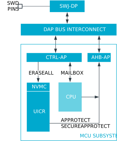
Access port protection (APPROTECT) blocks the debugger access to the AHB-AP, and prevents read and write access to all CPU registers and memory-mapped addresses. To enable port protection access for both secure and non-secure modes, use the registers SECUREAPPROTECT and APPROTECT respectively. The debugger can use the register APPROTECT.STATUS to read the status of secure and non-secure access port protection.
- Soft reset
- Erase all
- Mailbox interface
- Debug of protected devices
Reset request
Erase all
The erase all function lets the debugger trigger an erase of flash, user information configuration registers (UICR), RAM, all peripheral settings, and also removes the access port protection.
To trigger an erase all function, the debugger writes to the register ERASEALL. The register ERASEALLSTATUS will read as busy for the duration of the operation. After the next reset, the access port protection is removed.
If the debugger performs an erase all function on a slave MCU, the erase sequence will always erase the application MCU first, independently of how the application is protected, before erasing the slave MCU.
Erase all protection
It is possible to prevent the debugger from performing an erase all operation by writing to the UICR.ERASEPROTECT register. Once the register is configured and the device is reset, the CTRL-AP ERASEALL operation is disabled, and all flash write and erase operations are restricted to the firmware. In addition, it is still possible to write/erase from the debugger as long as the UICR.APPROTECT register is not set.
The register ERASEPROTECT.STATUS holds the status for erase protection.
Mailbox interface
CTRL-AP implements a mailbox interface which enables the CPU to communicate with a debugger over the SWD interface.
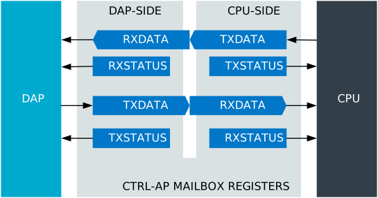
Mailbox transfer sequence
- Sender writes TXDATA.
- Hardware sets sender's TXSTATUS to DataPending.
- Hardware sets receiver's RXSTATUS to DataPending.
- Receiver reads RXDATA.
- Hardware sets receiver's RXSTATUS to NoDataPending.
- Hardware sets sender's TXSTATUS to NoDataPending.
Disabling erase protection
The erase protection mechanism can be disabled to return a device to factory default settings on next reset.
The debugger can read the erase protection status in the register ERASEPROTECT.STATUS.
If ERASEPROTECT has been enabled, both the debugger and on-chip firmware must write the same non-zero 32-bit KEY value into their respective ERASEPROTECT.DISABLE registers to disable the erase protection. When both registers have been written with the same non-zero 32-bit KEY value, the device is automatically erased as described in Erase all. The access ports will be re-enabled on the next reset once the secure erase sequence has completed.
The write-once register ERASEPROTECT.LOCK should be set to Locked as early as possible in the start-up sequence, preferably as soon as the on-chip firmware has determined it does not need to communicate with a debugger over the CTRL-AP mailbox interface. Once written, it will not be possible to remove the erase protection until the next reset.
Debugger registers
CTRL-AP has a set of registers that can only be accessed from the debugger over the SWD interface. These are not accessible from the CPU.
Debugger registers
Register overview
| Register | Offset | Description |
|---|---|---|
| RESET | 0x000 | System reset request |
| ERASEALL | 0x004 | Perform a secure erase of the device, where flash, SRAM and UICR will be erased in sequence. The device will be returned to factory default settings upon next reset. |
| ERASEALLSTATUS | 0x008 | This is the status register for the ERASEALL operation. |
| APPROTECT.STATUS | 0x00C | This is the status register for the UICR access port protection. |
| ERASEPROTECT.STATUS | 0x018 | This is the status register for the UICR ERASEPROTECT configuration. |
| ERASEPROTECT.DISABLE | 0x01C | This register disables ERASEPROTECT and performs ERASEALL. |
| MAILBOX.TXDATA | 0x020 | Data sent from the debugger to the CPU. |
| MAILBOX.TXSTATUS | 0x024 | This register shows a status that indicates if data sent from the debugger to the CPU has been read. |
| MAILBOX.RXDATA | 0x028 | Data sent from the CPU to the debugger. |
| MAILBOX.RXSTATUS | 0x02C | This register shows a status that indicates if data sent from the CPU to the debugger has been read. |
| IDR | 0x0FC | CTRL-AP Identification Register, IDR |
RESET
Address offset: 0x000
System reset request
This register is automatically deactivated during an ERASEALL operation.
| Bit number | 31 | 30 | 29 | 28 | 27 | 26 | 25 | 24 | 23 | 22 | 21 | 20 | 19 | 18 | 17 | 16 | 15 | 14 | 13 | 12 | 11 | 10 | 9 | 8 | 7 | 6 | 5 | 4 | 3 | 2 | 1 | 0 | |||
|---|---|---|---|---|---|---|---|---|---|---|---|---|---|---|---|---|---|---|---|---|---|---|---|---|---|---|---|---|---|---|---|---|---|---|---|
| ID | A | ||||||||||||||||||||||||||||||||||
| Reset 0x00000000 | 0 | 0 | 0 | 0 | 0 | 0 | 0 | 0 | 0 | 0 | 0 | 0 | 0 | 0 | 0 | 0 | 0 | 0 | 0 | 0 | 0 | 0 | 0 | 0 | 0 | 0 | 0 | 0 | 0 | 0 | 0 | 0 | |||
| ID | R/W | Field | Value ID | Value | Description | ||||||||||||||||||||||||||||||
| A | RW | RESET | System reset request and status | ||||||||||||||||||||||||||||||||
NoReset | 0 | Write to release reset Reading '0' means reset is not active | |||||||||||||||||||||||||||||||||
Reset | 1 | Write to hold reset Reading '1' means reset is active | |||||||||||||||||||||||||||||||||
ERASEALL
Address offset: 0x004
Perform a secure erase of the device, where flash, SRAM and UICR will be erased in sequence. The device will be returned to factory default settings upon next reset.
| Bit number | 31 | 30 | 29 | 28 | 27 | 26 | 25 | 24 | 23 | 22 | 21 | 20 | 19 | 18 | 17 | 16 | 15 | 14 | 13 | 12 | 11 | 10 | 9 | 8 | 7 | 6 | 5 | 4 | 3 | 2 | 1 | 0 | |||
|---|---|---|---|---|---|---|---|---|---|---|---|---|---|---|---|---|---|---|---|---|---|---|---|---|---|---|---|---|---|---|---|---|---|---|---|
| ID | A | ||||||||||||||||||||||||||||||||||
| Reset 0x00000000 | 0 | 0 | 0 | 0 | 0 | 0 | 0 | 0 | 0 | 0 | 0 | 0 | 0 | 0 | 0 | 0 | 0 | 0 | 0 | 0 | 0 | 0 | 0 | 0 | 0 | 0 | 0 | 0 | 0 | 0 | 0 | 0 | |||
| ID | R/W | Field | Value ID | Value | Description | ||||||||||||||||||||||||||||||
| A | W | ERASEALL | Return device to factory default settings | ||||||||||||||||||||||||||||||||
NoOperation | 0 | No operation | |||||||||||||||||||||||||||||||||
Erase | 1 | Erase flash, SRAM, and UICR in sequence | |||||||||||||||||||||||||||||||||
ERASEALLSTATUS
Address offset: 0x008
This is the status register for the ERASEALL operation.
| Bit number | 31 | 30 | 29 | 28 | 27 | 26 | 25 | 24 | 23 | 22 | 21 | 20 | 19 | 18 | 17 | 16 | 15 | 14 | 13 | 12 | 11 | 10 | 9 | 8 | 7 | 6 | 5 | 4 | 3 | 2 | 1 | 0 | |||
|---|---|---|---|---|---|---|---|---|---|---|---|---|---|---|---|---|---|---|---|---|---|---|---|---|---|---|---|---|---|---|---|---|---|---|---|
| ID | A | ||||||||||||||||||||||||||||||||||
| Reset 0x00000000 | 0 | 0 | 0 | 0 | 0 | 0 | 0 | 0 | 0 | 0 | 0 | 0 | 0 | 0 | 0 | 0 | 0 | 0 | 0 | 0 | 0 | 0 | 0 | 0 | 0 | 0 | 0 | 0 | 0 | 0 | 0 | 0 | |||
| ID | R/W | Field | Value ID | Value | Description | ||||||||||||||||||||||||||||||
| A | R | ERASEALLSTATUS | Status bit for the ERASEALL operation | ||||||||||||||||||||||||||||||||
Ready | 0 | ERASEALL is ready | |||||||||||||||||||||||||||||||||
Busy | 1 | ERASEALL is busy (on-going) | |||||||||||||||||||||||||||||||||
APPROTECT.STATUS
Address offset: 0x00C
This is the status register for the UICR access port protection.
| Bit number | 31 | 30 | 29 | 28 | 27 | 26 | 25 | 24 | 23 | 22 | 21 | 20 | 19 | 18 | 17 | 16 | 15 | 14 | 13 | 12 | 11 | 10 | 9 | 8 | 7 | 6 | 5 | 4 | 3 | 2 | 1 | 0 | |||
|---|---|---|---|---|---|---|---|---|---|---|---|---|---|---|---|---|---|---|---|---|---|---|---|---|---|---|---|---|---|---|---|---|---|---|---|
| ID | B | A | |||||||||||||||||||||||||||||||||
| Reset 0x00000000 | 0 | 0 | 0 | 0 | 0 | 0 | 0 | 0 | 0 | 0 | 0 | 0 | 0 | 0 | 0 | 0 | 0 | 0 | 0 | 0 | 0 | 0 | 0 | 0 | 0 | 0 | 0 | 0 | 0 | 0 | 0 | 0 | |||
| ID | R/W | Field | Value ID | Value | Description | ||||||||||||||||||||||||||||||
| A | R | APPROTECT | Status bit for access port protection Note: The reset value is auto read from the APPROTECT register in UICR. | ||||||||||||||||||||||||||||||||
Enabled | 0 | APPROTECT is enabled | |||||||||||||||||||||||||||||||||
Disabled | 1 | APPROTECT is disabled | |||||||||||||||||||||||||||||||||
| B | R | SECUREAPPROTECT | Status bit for secure access port protection Note: The reset value is auto read from the SECUREAPPROTECT register in UICR. | ||||||||||||||||||||||||||||||||
Enabled | 0 | SECUREAPPROTECT is enabled | |||||||||||||||||||||||||||||||||
Disabled | 1 | SECUREAPPROTECT is disabled | |||||||||||||||||||||||||||||||||
ERASEPROTECT.STATUS
Address offset: 0x018
This is the status register for the UICR ERASEPROTECT configuration.
| Bit number | 31 | 30 | 29 | 28 | 27 | 26 | 25 | 24 | 23 | 22 | 21 | 20 | 19 | 18 | 17 | 16 | 15 | 14 | 13 | 12 | 11 | 10 | 9 | 8 | 7 | 6 | 5 | 4 | 3 | 2 | 1 | 0 | |||
|---|---|---|---|---|---|---|---|---|---|---|---|---|---|---|---|---|---|---|---|---|---|---|---|---|---|---|---|---|---|---|---|---|---|---|---|
| ID | A | ||||||||||||||||||||||||||||||||||
| Reset 0x00000000 | 0 | 0 | 0 | 0 | 0 | 0 | 0 | 0 | 0 | 0 | 0 | 0 | 0 | 0 | 0 | 0 | 0 | 0 | 0 | 0 | 0 | 0 | 0 | 0 | 0 | 0 | 0 | 0 | 0 | 0 | 0 | 0 | |||
| ID | R/W | Field | Value ID | Value | Description | ||||||||||||||||||||||||||||||
| A | R | PALL | Status bit for erase protection Note: The reset value is auto read from the ERASEPROTECT register in UICR. | ||||||||||||||||||||||||||||||||
Enabled | 0 | ERASEPROTECT is enabled | |||||||||||||||||||||||||||||||||
Disabled | 1 | ERASEPROTECT is not enabled and ERASEALL can be performed | |||||||||||||||||||||||||||||||||
ERASEPROTECT.DISABLE
Address offset: 0x01C
This register disables ERASEPROTECT and performs ERASEALL.
| Bit number | 31 | 30 | 29 | 28 | 27 | 26 | 25 | 24 | 23 | 22 | 21 | 20 | 19 | 18 | 17 | 16 | 15 | 14 | 13 | 12 | 11 | 10 | 9 | 8 | 7 | 6 | 5 | 4 | 3 | 2 | 1 | 0 | |||
|---|---|---|---|---|---|---|---|---|---|---|---|---|---|---|---|---|---|---|---|---|---|---|---|---|---|---|---|---|---|---|---|---|---|---|---|
| ID | A | A | A | A | A | A | A | A | A | A | A | A | A | A | A | A | A | A | A | A | A | A | A | A | A | A | A | A | A | A | A | A | |||
| Reset 0x00000000 | 0 | 0 | 0 | 0 | 0 | 0 | 0 | 0 | 0 | 0 | 0 | 0 | 0 | 0 | 0 | 0 | 0 | 0 | 0 | 0 | 0 | 0 | 0 | 0 | 0 | 0 | 0 | 0 | 0 | 0 | 0 | 0 | |||
| ID | R/W | Field | Value ID | Value | Description | ||||||||||||||||||||||||||||||
| A | RW1 | KEY | The ERASEALL sequence will be initiated if value of the KEY fields are non-zero and the KEY fields match on both the CPU and debugger sides. | ||||||||||||||||||||||||||||||||
MAILBOX.TXDATA
Address offset: 0x020
Data sent from the debugger to the CPU.
Writing to this register will automatically set a DataPending value in the TXSTATUS register.
| Bit number | 31 | 30 | 29 | 28 | 27 | 26 | 25 | 24 | 23 | 22 | 21 | 20 | 19 | 18 | 17 | 16 | 15 | 14 | 13 | 12 | 11 | 10 | 9 | 8 | 7 | 6 | 5 | 4 | 3 | 2 | 1 | 0 | |||
|---|---|---|---|---|---|---|---|---|---|---|---|---|---|---|---|---|---|---|---|---|---|---|---|---|---|---|---|---|---|---|---|---|---|---|---|
| ID | A | A | A | A | A | A | A | A | A | A | A | A | A | A | A | A | A | A | A | A | A | A | A | A | A | A | A | A | A | A | A | A | |||
| Reset 0x00000000 | 0 | 0 | 0 | 0 | 0 | 0 | 0 | 0 | 0 | 0 | 0 | 0 | 0 | 0 | 0 | 0 | 0 | 0 | 0 | 0 | 0 | 0 | 0 | 0 | 0 | 0 | 0 | 0 | 0 | 0 | 0 | 0 | |||
| ID | R/W | Field | Value ID | Value | Description | ||||||||||||||||||||||||||||||
| A | RW | Data | Data sent from debugger | ||||||||||||||||||||||||||||||||
MAILBOX.TXSTATUS
Address offset: 0x024
This register shows a status that indicates if data sent from the debugger to the CPU has been read.
| Bit number | 31 | 30 | 29 | 28 | 27 | 26 | 25 | 24 | 23 | 22 | 21 | 20 | 19 | 18 | 17 | 16 | 15 | 14 | 13 | 12 | 11 | 10 | 9 | 8 | 7 | 6 | 5 | 4 | 3 | 2 | 1 | 0 | |||
|---|---|---|---|---|---|---|---|---|---|---|---|---|---|---|---|---|---|---|---|---|---|---|---|---|---|---|---|---|---|---|---|---|---|---|---|
| ID | A | ||||||||||||||||||||||||||||||||||
| Reset 0x00000000 | 0 | 0 | 0 | 0 | 0 | 0 | 0 | 0 | 0 | 0 | 0 | 0 | 0 | 0 | 0 | 0 | 0 | 0 | 0 | 0 | 0 | 0 | 0 | 0 | 0 | 0 | 0 | 0 | 0 | 0 | 0 | 0 | |||
| ID | R/W | Field | Value ID | Value | Description | ||||||||||||||||||||||||||||||
| A | R | Status | Status of register DATA | ||||||||||||||||||||||||||||||||
NoDataPending | 0 | No data pending in register TXDATA | |||||||||||||||||||||||||||||||||
DataPending | 1 | Data pending in register TXDATA | |||||||||||||||||||||||||||||||||
MAILBOX.RXDATA
Address offset: 0x028
Data sent from the CPU to the debugger.
Reading from this register will automatically set a NoDataPending value in the RXSTATUS register.
| Bit number | 31 | 30 | 29 | 28 | 27 | 26 | 25 | 24 | 23 | 22 | 21 | 20 | 19 | 18 | 17 | 16 | 15 | 14 | 13 | 12 | 11 | 10 | 9 | 8 | 7 | 6 | 5 | 4 | 3 | 2 | 1 | 0 | |||
|---|---|---|---|---|---|---|---|---|---|---|---|---|---|---|---|---|---|---|---|---|---|---|---|---|---|---|---|---|---|---|---|---|---|---|---|
| ID | A | A | A | A | A | A | A | A | A | A | A | A | A | A | A | A | A | A | A | A | A | A | A | A | A | A | A | A | A | A | A | A | |||
| Reset 0x00000000 | 0 | 0 | 0 | 0 | 0 | 0 | 0 | 0 | 0 | 0 | 0 | 0 | 0 | 0 | 0 | 0 | 0 | 0 | 0 | 0 | 0 | 0 | 0 | 0 | 0 | 0 | 0 | 0 | 0 | 0 | 0 | 0 | |||
| ID | R/W | Field | Value ID | Value | Description | ||||||||||||||||||||||||||||||
| A | R | Data | Data sent from CPU | ||||||||||||||||||||||||||||||||
MAILBOX.RXSTATUS
Address offset: 0x02C
This register shows a status that indicates if data sent from the CPU to the debugger has been read.
| Bit number | 31 | 30 | 29 | 28 | 27 | 26 | 25 | 24 | 23 | 22 | 21 | 20 | 19 | 18 | 17 | 16 | 15 | 14 | 13 | 12 | 11 | 10 | 9 | 8 | 7 | 6 | 5 | 4 | 3 | 2 | 1 | 0 | |||
|---|---|---|---|---|---|---|---|---|---|---|---|---|---|---|---|---|---|---|---|---|---|---|---|---|---|---|---|---|---|---|---|---|---|---|---|
| ID | A | ||||||||||||||||||||||||||||||||||
| Reset 0x00000000 | 0 | 0 | 0 | 0 | 0 | 0 | 0 | 0 | 0 | 0 | 0 | 0 | 0 | 0 | 0 | 0 | 0 | 0 | 0 | 0 | 0 | 0 | 0 | 0 | 0 | 0 | 0 | 0 | 0 | 0 | 0 | 0 | |||
| ID | R/W | Field | Value ID | Value | Description | ||||||||||||||||||||||||||||||
| A | R | Status | Status of register DATA | ||||||||||||||||||||||||||||||||
NoDataPending | 0 | No data pending in register RXDATA | |||||||||||||||||||||||||||||||||
DataPending | 1 | Data pending in register RXDATA | |||||||||||||||||||||||||||||||||
IDR
Address offset: 0x0FC
CTRL-AP Identification Register, IDR
| Bit number | 31 | 30 | 29 | 28 | 27 | 26 | 25 | 24 | 23 | 22 | 21 | 20 | 19 | 18 | 17 | 16 | 15 | 14 | 13 | 12 | 11 | 10 | 9 | 8 | 7 | 6 | 5 | 4 | 3 | 2 | 1 | 0 | |||
|---|---|---|---|---|---|---|---|---|---|---|---|---|---|---|---|---|---|---|---|---|---|---|---|---|---|---|---|---|---|---|---|---|---|---|---|
| ID | E | E | E | E | D | D | D | D | C | C | C | C | C | C | C | B | B | B | B | A | A | A | A | A | A | A | A | ||||||||
| Reset 0x12880000 | 0 | 0 | 0 | 1 | 0 | 0 | 1 | 0 | 1 | 0 | 0 | 0 | 1 | 0 | 0 | 0 | 0 | 0 | 0 | 0 | 0 | 0 | 0 | 0 | 0 | 0 | 0 | 0 | 0 | 0 | 0 | 0 | |||
| ID | R/W | Field | Value ID | Value | Description | ||||||||||||||||||||||||||||||
| A | R | APID | AP Identification | ||||||||||||||||||||||||||||||||
| B | R | CLASS | Access Port (AP) class | ||||||||||||||||||||||||||||||||
NotDefined | 0x0 | No defined class | |||||||||||||||||||||||||||||||||
MEMAP | 0x8 | Memory Access Port | |||||||||||||||||||||||||||||||||
| C | R | JEP106ID | JEDEC JEP106 identity code | ||||||||||||||||||||||||||||||||
| D | R | JEP106CONT | JEDEC JEP106 continuation code | ||||||||||||||||||||||||||||||||
| E | R | REVISION | Revision | ||||||||||||||||||||||||||||||||
Registers
Instances
| Instance | Base address | TrustZone | Split access | Description | ||
|---|---|---|---|---|---|---|
| Map | Att | DMA | ||||
| CTRL_AP_PERI | 0x50006000 | HF | S | NA | No | CTRL-AP-PERI |
Register overview
| Register | Offset | TZ | Description |
|---|---|---|---|
| MAILBOX.RXDATA | 0x400 | Data sent from the debugger to the CPU. | |
| MAILBOX.RXSTATUS | 0x404 | This register shows a status that indicates if data sent from the debugger to the CPU has been read. | |
| MAILBOX.TXDATA | 0x480 | Data sent from the CPU to the debugger. | |
| MAILBOX.TXSTATUS | 0x484 | This register shows a status that indicates if the data sent from the CPU to the debugger has been read. | |
| ERASEPROTECT.LOCK | 0x500 | This register locks the ERASEPROTECT.DISABLE register from being written until next reset. | |
| ERASEPROTECT.DISABLE | 0x504 | This register disables the ERASEPROTECT register and performs an ERASEALL operation. |
MAILBOX.RXDATA
Address offset: 0x400
Data sent from the debugger to the CPU.
Reading from this register will automatically set a NoDataPending value in the RXSTATUS register.
| Bit number | 31 | 30 | 29 | 28 | 27 | 26 | 25 | 24 | 23 | 22 | 21 | 20 | 19 | 18 | 17 | 16 | 15 | 14 | 13 | 12 | 11 | 10 | 9 | 8 | 7 | 6 | 5 | 4 | 3 | 2 | 1 | 0 | |||
|---|---|---|---|---|---|---|---|---|---|---|---|---|---|---|---|---|---|---|---|---|---|---|---|---|---|---|---|---|---|---|---|---|---|---|---|
| ID | A | A | A | A | A | A | A | A | A | A | A | A | A | A | A | A | A | A | A | A | A | A | A | A | A | A | A | A | A | A | A | A | |||
| Reset 0x00000000 | 0 | 0 | 0 | 0 | 0 | 0 | 0 | 0 | 0 | 0 | 0 | 0 | 0 | 0 | 0 | 0 | 0 | 0 | 0 | 0 | 0 | 0 | 0 | 0 | 0 | 0 | 0 | 0 | 0 | 0 | 0 | 0 | |||
| ID | R/W | Field | Value ID | Value | Description | ||||||||||||||||||||||||||||||
| A | R | RXDATA | Data received from debugger | ||||||||||||||||||||||||||||||||
MAILBOX.RXSTATUS
Address offset: 0x404
This register shows a status that indicates if data sent from the debugger to the CPU has been read.
| Bit number | 31 | 30 | 29 | 28 | 27 | 26 | 25 | 24 | 23 | 22 | 21 | 20 | 19 | 18 | 17 | 16 | 15 | 14 | 13 | 12 | 11 | 10 | 9 | 8 | 7 | 6 | 5 | 4 | 3 | 2 | 1 | 0 | |||
|---|---|---|---|---|---|---|---|---|---|---|---|---|---|---|---|---|---|---|---|---|---|---|---|---|---|---|---|---|---|---|---|---|---|---|---|
| ID | A | ||||||||||||||||||||||||||||||||||
| Reset 0x00000000 | 0 | 0 | 0 | 0 | 0 | 0 | 0 | 0 | 0 | 0 | 0 | 0 | 0 | 0 | 0 | 0 | 0 | 0 | 0 | 0 | 0 | 0 | 0 | 0 | 0 | 0 | 0 | 0 | 0 | 0 | 0 | 0 | |||
| ID | R/W | Field | Value ID | Value | Description | ||||||||||||||||||||||||||||||
| A | R | RXSTATUS | Status of data in register RXDATA | ||||||||||||||||||||||||||||||||
NoDataPending | 0 | No data pending in register RXDATA | |||||||||||||||||||||||||||||||||
DataPending | 1 | Data pending in register RXDATA | |||||||||||||||||||||||||||||||||
MAILBOX.TXDATA
Address offset: 0x480
Data sent from the CPU to the debugger.
Writing to this register will automatically set a DataPending value in the TXSTATUS register.
| Bit number | 31 | 30 | 29 | 28 | 27 | 26 | 25 | 24 | 23 | 22 | 21 | 20 | 19 | 18 | 17 | 16 | 15 | 14 | 13 | 12 | 11 | 10 | 9 | 8 | 7 | 6 | 5 | 4 | 3 | 2 | 1 | 0 | |||
|---|---|---|---|---|---|---|---|---|---|---|---|---|---|---|---|---|---|---|---|---|---|---|---|---|---|---|---|---|---|---|---|---|---|---|---|
| ID | A | A | A | A | A | A | A | A | A | A | A | A | A | A | A | A | A | A | A | A | A | A | A | A | A | A | A | A | A | A | A | A | |||
| Reset 0x00000000 | 0 | 0 | 0 | 0 | 0 | 0 | 0 | 0 | 0 | 0 | 0 | 0 | 0 | 0 | 0 | 0 | 0 | 0 | 0 | 0 | 0 | 0 | 0 | 0 | 0 | 0 | 0 | 0 | 0 | 0 | 0 | 0 | |||
| ID | R/W | Field | Value ID | Value | Description | ||||||||||||||||||||||||||||||
| A | RW | TXDATA | Data sent to debugger | ||||||||||||||||||||||||||||||||
MAILBOX.TXSTATUS
Address offset: 0x484
This register shows a status that indicates if the data sent from the CPU to the debugger has been read.
| Bit number | 31 | 30 | 29 | 28 | 27 | 26 | 25 | 24 | 23 | 22 | 21 | 20 | 19 | 18 | 17 | 16 | 15 | 14 | 13 | 12 | 11 | 10 | 9 | 8 | 7 | 6 | 5 | 4 | 3 | 2 | 1 | 0 | |||
|---|---|---|---|---|---|---|---|---|---|---|---|---|---|---|---|---|---|---|---|---|---|---|---|---|---|---|---|---|---|---|---|---|---|---|---|
| ID | A | ||||||||||||||||||||||||||||||||||
| Reset 0x00000000 | 0 | 0 | 0 | 0 | 0 | 0 | 0 | 0 | 0 | 0 | 0 | 0 | 0 | 0 | 0 | 0 | 0 | 0 | 0 | 0 | 0 | 0 | 0 | 0 | 0 | 0 | 0 | 0 | 0 | 0 | 0 | 0 | |||
| ID | R/W | Field | Value ID | Value | Description | ||||||||||||||||||||||||||||||
| A | R | TXSTATUS | Status of data in register TXDATA | ||||||||||||||||||||||||||||||||
NoDataPending | 0 | No data pending in register TXDATA | |||||||||||||||||||||||||||||||||
DataPending | 1 | Data pending in register TXDATA | |||||||||||||||||||||||||||||||||
ERASEPROTECT.LOCK
Address offset: 0x500
This register locks the ERASEPROTECT.DISABLE register from being written until next reset.
| Bit number | 31 | 30 | 29 | 28 | 27 | 26 | 25 | 24 | 23 | 22 | 21 | 20 | 19 | 18 | 17 | 16 | 15 | 14 | 13 | 12 | 11 | 10 | 9 | 8 | 7 | 6 | 5 | 4 | 3 | 2 | 1 | 0 | |||
|---|---|---|---|---|---|---|---|---|---|---|---|---|---|---|---|---|---|---|---|---|---|---|---|---|---|---|---|---|---|---|---|---|---|---|---|
| ID | A | ||||||||||||||||||||||||||||||||||
| Reset 0x00000000 | 0 | 0 | 0 | 0 | 0 | 0 | 0 | 0 | 0 | 0 | 0 | 0 | 0 | 0 | 0 | 0 | 0 | 0 | 0 | 0 | 0 | 0 | 0 | 0 | 0 | 0 | 0 | 0 | 0 | 0 | 0 | 0 | |||
| ID | R/W | Field | Value ID | Value | Description | ||||||||||||||||||||||||||||||
| A | RW1 | LOCK | Lock ERASEPROTECT.DISABLE register from being written until next reset | ||||||||||||||||||||||||||||||||
Unlocked | 0 | Register ERASEPROTECT.DISABLE is writeable | |||||||||||||||||||||||||||||||||
Locked | 1 | Register ERASEPROTECT.DISABLE is read-only | |||||||||||||||||||||||||||||||||
ERASEPROTECT.DISABLE
Address offset: 0x504
This register disables the ERASEPROTECT register and performs an ERASEALL operation.
| Bit number | 31 | 30 | 29 | 28 | 27 | 26 | 25 | 24 | 23 | 22 | 21 | 20 | 19 | 18 | 17 | 16 | 15 | 14 | 13 | 12 | 11 | 10 | 9 | 8 | 7 | 6 | 5 | 4 | 3 | 2 | 1 | 0 | |||
|---|---|---|---|---|---|---|---|---|---|---|---|---|---|---|---|---|---|---|---|---|---|---|---|---|---|---|---|---|---|---|---|---|---|---|---|
| ID | A | A | A | A | A | A | A | A | A | A | A | A | A | A | A | A | A | A | A | A | A | A | A | A | A | A | A | A | A | A | A | A | |||
| Reset 0x00000000 | 0 | 0 | 0 | 0 | 0 | 0 | 0 | 0 | 0 | 0 | 0 | 0 | 0 | 0 | 0 | 0 | 0 | 0 | 0 | 0 | 0 | 0 | 0 | 0 | 0 | 0 | 0 | 0 | 0 | 0 | 0 | 0 | |||
| ID | R/W | Field | Value ID | Value | Description | ||||||||||||||||||||||||||||||
| A | RW1 | KEY | The ERASEALL sequence is initiated if the value of the KEY fields are non-zero and the KEY fields match on both the CPU and debugger sides. | ||||||||||||||||||||||||||||||||