2. System Description
This chapter describes the RP2040 key system features including processor, memory, how blocks are connected, clocks, resets, power, and IO. Refer to Figure 2 for an overview diagram.
2.1. Bus Fabric
The RP2040 bus fabric routes addresses and data across the chip.
Figure 4 shows the high-level structure of the bus fabric. The main AHB-Lite crossbar routes addresses and data between its 4 upstream ports and 10 downstream ports: up to four bus transfers can take place each cycle. All data paths are 32 bits wide. Memory devices have dedicated ports on the main crossbar, to satisfy their high bandwidth requirements. High-bandwidth AHB-Lite peripherals have a shared port on the crossbar, and an APB bridge provides bus access to system control registers and lower-bandwidth peripherals.
Figure 4. RP2040 bus fabric overview.
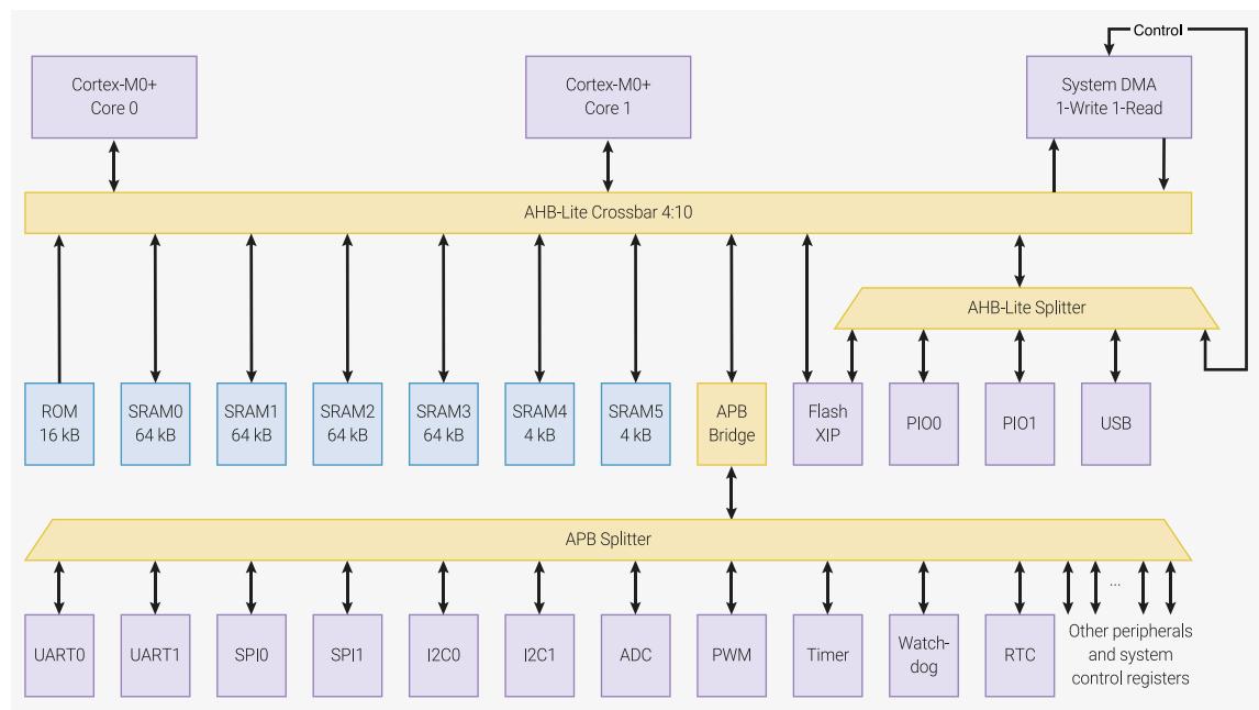
The bus fabric connects 4 AHB-Lite masters, i.e. devices which generate addresses:
- • Processor core 0
- • Processor core 1
- • DMA controller Read port
- • DMA controller Write port
These are routed through to 10 downstream ports on the main crossbar:
- • ROM
- • Flash XIP
- • SRAM 0 to 5 (one port each)
- • Fast AHB-Lite peripherals: PI00, PI01, USB, DMA control registers, XIP aux (one shared port)
- • Bridge to all APB peripherals, and system control registers
The four bus masters can access any four different crossbar ports simultaneously, the bus fabric does not add wait
states to any AHB-Lite slave access. So at a system clock of 125MHz the maximum sustained bus bandwidth is 2.0GBps. The system address map has been arranged to make this parallel bandwidth available to as many software use cases as possible – for example, the striped SRAM alias ( Section 2.6.2 ) scatters main memory accesses across four crossbar ports (SRAM0...3), so that more memory accesses can proceed in parallel.
2.1.1. AHB-Lite Crossbar
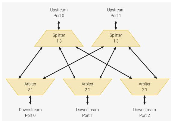
At the centre of the RP2040 bus fabric is a 4:10 fully-connected crossbar. Its 4 upstream ports are connected to the 4 system bus masters, and the 10 downstream ports connect to the highest-bandwidth AHB-Lite slaves (namely the memory interfaces) and to lower layers of the fabric. Figure 5 shows the structure of a 2:3 AHB-Lite crossbar, arranged identically to the 4:10 crossbar on RP2040, but easier to show in the diagram.
Figure 5. A 2:3 AHB-Lite crossbar. Each upstream port connects to a splitter, which routes bus requests toward one of the 3 downstream ports, and routes responses back. Each downstream port connects to an arbiter, which safely manages concurrent access to the port.
graph TD
    U0[Upstream Port 0] <--> S0[Splitter 1:3]
    U1[Upstream Port 1] <--> S1[Splitter 1:3]
    S0 --> A0[Arbiter 2:1]
    S0 --> A1[Arbiter 2:1]
    S0 --> A2[Arbiter 2:1]
    S1 --> A0
    S1 --> A1
    S1 --> A2
    A0 <--> D0[Downstream Port 0]
    A1 <--> D1[Downstream Port 1]
    A2 <--> D2[Downstream Port 2]
The crossbar is built from two components:
- • Splitters
- ◦ Perform coarse address decode
- ◦ Route requests (addresses, write data) to the downstream port indicated by the initial address decode
- ◦ Route responses (read data, bus errors) from the correct arbiter back to the upstream port
- • Arbiters
- ◦ Manage concurrent requests to a downstream port
- ◦ Route responses (read data, bus errors) to the correct splitter
- ◦ Implement bus priority rules
The main crossbar on RP2040 consists of 4 1:10 splitters and 10 4:1 arbiters, with a mesh of 40 AHB-Lite bus channels between them. Note that, as AHB-Lite is a pipelined bus, the splitter may be routing back a response to an earlier request from downstream port A, whilst a new request to downstream port B is already in progress. This does not incur any cycle penalty.
2.1.1.1. Bus Priority
The arbiters in the main AHB-Lite crossbar implement a two-level bus priority scheme. Priority levels are configured per-master, using the BUS_PRIORITY register in the BUSCTRL register block.
When there are multiple simultaneous accesses to same arbiter, any requests from high-priority masters (priority level 1) will be considered before any requests from low-priority masters (priority 0). If multiple masters of the same priority level attempt to access the same slave simultaneously, a round-robin tie break is applied, i.e. the arbiter grants access to each master in turn.
NOTEPriority arbitration only applies to multiple masters attempting to access the same slave on the same cycle. Accesses to different slaves, e.g. different SRAM banks, can proceed simultaneously.
When accessing a slave with zero wait states, such as SRAM (i.e. can be accessed once per system clock cycle), high-priority masters will never observe any slowdown or other timing effects caused by accesses from low-priority masters. This allows guaranteed latency and throughput for hard real time use cases; it does however mean a low-priority master may get stalled until there is a free cycle.
2.1.1.2. Bus Performance Counters
The performance counters automatically count accesses to the main AHB-Lite crossbar arbiters. This can assist in diagnosing performance issues, in high-traffic use cases.
There are four performance counters. Each is a 24-bit saturating counter. Counter values can be read from
BUSCTRL_PERFCTR
x
, and cleared by writing any value to
BUSCTRL_PERFCTR
x
. Each counter can count one of the 20 available events at a time, as selected by
BUSCTRL_PERFSEL
x
. The available bus events are:
| PERFSEL x | Event | Description |
|---|---|---|
| 0 | APB access, contested | Completion of an access to the APB arbiter (which is upstream of all APB peripherals), which was previously delayed due to an access by another master. |
| 1 | APB access | Completion of an access to the APB arbiter |
| 2 | FASTPERI access, contested | Completion of an access to the FASTPERI arbiter (which is upstream of PIOs, DMA config port, USB, XIP aux FIFO port), which was previously delayed due to an access by another master. |
| 3 | FASTPERI access | Completion of an access to the FASTPERI arbiter |
| 4 | SRAM5 access, contested | Completion of an access to the SRAM5 arbiter, which was previously delayed due to an access by another master. |
| 5 | SRAM5 access | Completion of an access to the SRAM5 arbiter |
| 6 | SRAM4 access, contested | Completion of an access to the SRAM4 arbiter, which was previously delayed due to an access by another master. |
| 7 | SRAM4 access | Completion of an access to the SRAM4 arbiter |
| 8 | SRAM3 access, contested | Completion of an access to the SRAM3 arbiter, which was previously delayed due to an access by another master. |
| 9 | SRAM3 access | Completion of an access to the SRAM3 arbiter |
| 10 | SRAM2 access, contested | Completion of an access to the SRAM2 arbiter, which was previously delayed due to an access by another master. |
| 11 | SRAM2 access | Completion of an access to the SRAM2 arbiter |
| 12 | SRAM1 access, contested | Completion of an access to the SRAM1 arbiter, which was previously delayed due to an access by another master. |
| 13 | SRAM1 access | Completion of an access to the SRAM1 arbiter |
| 14 | SRAM0 access, contested | Completion of an access to the SRAM0 arbiter, which was previously delayed due to an access by another master. |
| 15 | SRAM0 access | Completion of an access to the SRAM0 arbiter |
| PERFSEL x | Event | Description |
|---|---|---|
| 16 | XIP_MAIN access, contested | Completion of an access to the XIP_MAIN arbiter, which was previously delayed due to an access by another master. |
| 17 | XIP_MAIN access | Completion of an access to the XIP_MAIN arbiter |
| 18 | ROM access, contested | Completion of an access to the ROM arbiter, which was previously delayed due to an access by another master. |
| 19 | ROM access | Completion of an access to the ROM arbiter |
2.1.2. Atomic Register Access
Each peripheral register block is allocated 4kB of address space, with registers accessed using one of 4 methods, selected by address decode.
- • Addr + 0x0000 : normal read write access
- • Addr + 0x1000 : atomic XOR on write
- • Addr + 0x2000 : atomic bitmask set on write
- • Addr + 0x3000 : atomic bitmask clear on write
This allows individual fields of a control register to be modified without performing a read-modify-write sequence in software: instead the changes are posted to the peripheral, and performed in-situ. Without this capability, it is difficult to safely access IO registers when an interrupt service routine is concurrent with code running in the foreground, or when the two processors are running code in parallel.
The four atomic access aliases occupy a total of 16kB. Most peripherals on RP2040 provide this functionality natively, and atomic writes have the same timing as normal read/write access. Some peripherals (I2C, UART, SPI and SSI) instead have this functionality added using a bus interposer, which translates upstream atomic writes into downstream read-modify-write sequences, at the boundary of the peripheral. This extends the access time by two system clock cycles.
The SIO ( Section 2.3.1 ), a single-cycle IO block attached directly to the cores' IO ports, does not support atomic accesses at the bus level, although some individual registers (e.g. GPIO) have set/clear/xor aliases.
2.1.3. APB Bridge
The APB bridge interfaces the high-speed main AHB-Lite interconnect to the lower-bandwidth peripherals. Whilst the AHB-Lite fabric offers zero-wait-state access everywhere, APB accesses have a cycle penalty:
- • APB bus accesses take two cycles minimum (setup phase and access phase)
- • The bridge adds an additional cycle to read accesses, as the bus request and response are registered
- • The bridge adds two additional cycles to write accesses, as the APB setup phase can not begin until the AHB-Lite write data is valid
As a result, the throughput of the APB portion of the bus fabric is somewhat lower than the AHB-Lite portion. However, there is more than sufficient bandwidth to saturate the APB serial peripherals.
2.1.4. Narrow IO Register Writes
Memory-mapped IO registers on RP2040 ignore the width of bus read/write accesses. They treat all writes as though they were 32 bits in size. This means software can not use byte or halfword writes to modify part of an IO register: any write to an address where the 30 address MSBs match the register address will affect the contents of the entire
register.
To update part of an IO register, without a read-modify-write sequence, the best solution on RP2040 is atomic set/clear/XOR (see Section 2.1.2 ). Note that this is more flexible than byte or halfword writes, as any combination of fields can be updated in one operation.
Upon a 8-bit or 16-bit write (such as a
strb
instruction on the Cortex-M0+), an IO register will sample the entire 32-bit write databus. The Cortex-M0+ and DMA on RP2040 will always replicate narrow data across the bus:
Pico Examples: https://github.com/raspberrypi/pico-examples/blob/master/system/narrow_io_write/narrow_io_write.c Lines 19 - 62
19 int main() {
20     stdio_init_all();
21
22     // We'll use WATCHDOG_SCRATCH0 as a convenient 32 bit read/write register
23     // that we can assign arbitrary values to
24     io_rw_32 *scratch32 = &watchdog_hw->scratch[0];
25     // Alias the scratch register as two halfwords at offsets +0x0 and +0x2
26     volatile uint16_t *scratch16 = (volatile uint16_t *) scratch32;
27     // Alias the scratch register as four bytes at offsets +0x0, +0x1, +0x2, +0x3:
28     volatile uint8_t *scratch8 = (volatile uint8_t *) scratch32;
29
30     // Show that we can read/write the scratch register as normal:
31     printf("Writing 32 bit value\n");
32     *scratch32 = 0xdeadbeef;
33     printf("Should be 0xdeadbeef: 0x%08x\n", *scratch32);
34
35     // We can do narrow reads just fine -- IO registers treat this as a 32 bit
36     // read, and the processor/DMA will pick out the correct byte lanes based
37     // on transfer size and address LSBs
38     printf("\nReading back 1 byte at a time\n");
39     // Little-endian!
40     printf("Should be ef be ad de: %02x ", scratch8[0]);
41     printf("%02x ", scratch8[1]);
42     printf("%02x ", scratch8[2]);
43     printf("%02x\n", scratch8[3]);
44
45     // Byte writes are replicated four times across the 32-bit bus, and IO
46     // registers usually sample the entire write bus.
47     printf("\nWriting 8 bit value 0xa5 at offset 0\n");
48     scratch8[0] = 0xa5;
49     // Read back the whole scratch register in one go
50     printf("Should be 0xa5a5a5a5: 0x%08x\n", *scratch32);
51
52     // The IO register ignores the address LSBs [1:0] as well as the transfer
53     // size, so it doesn't matter what byte offset we use
54     printf("\nWriting 8 bit value at offset 1\n");
55     scratch8[1] = 0x3c;
56     printf("Should be 0x3c3c3c3c: 0x%08x\n", *scratch32);
57
58     // Halfword writes are also replicated across the write data bus
59     printf("\nWriting 16 bit value at offset 0\n");
60     scratch16[0] = 0xf00d;
61     printf("Should be 0xf00df00d: 0x%08x\n", *scratch32);
62 }
2.1.5. List of Registers
The Bus Fabric registers start at a base address of
0x40030000
(defined as
BUSCTRL_BASE
in SDK).
Table 4. List of
BUSCTRL registers
| Offset | Name | Info |
|---|---|---|
| 0x00 | BUS_PRIORITY | Set the priority of each master for bus arbitration. |
| 0x04 | BUS_PRIORITY_ACK | Bus priority acknowledge |
| 0x08 | PERFCTR0 | Bus fabric performance counter 0 |
| 0x0c | PERFSEL0 | Bus fabric performance event select for PERFCTR0 |
| 0x10 | PERFCTR1 | Bus fabric performance counter 1 |
| 0x14 | PERFSEL1 | Bus fabric performance event select for PERFCTR1 |
| 0x18 | PERFCTR2 | Bus fabric performance counter 2 |
| 0x1c | PERFSEL2 | Bus fabric performance event select for PERFCTR2 |
| 0x20 | PERFCTR3 | Bus fabric performance counter 3 |
| 0x24 | PERFSEL3 | Bus fabric performance event select for PERFCTR3 |
BUSCTRL: BUS_PRIORITY Register
Offset: 0x00
Description
Set the priority of each master for bus arbitration.
Table 5.
BUS_PRIORITY
Register
| Bits | Description | Type | Reset |
|---|---|---|---|
| 31:13 | Reserved. | - | - |
| 12 | DMA_W : 0 - low priority, 1 - high priority | RW | 0x0 |
| 11:9 | Reserved. | - | - |
| 8 | DMA_R : 0 - low priority, 1 - high priority | RW | 0x0 |
| 7:5 | Reserved. | - | - |
| 4 | PROC1 : 0 - low priority, 1 - high priority | RW | 0x0 |
| 3:1 | Reserved. | - | - |
| 0 | PROC0 : 0 - low priority, 1 - high priority | RW | 0x0 |
BUSCTRL: BUS_PRIORITY_ACK Register
Offset: 0x04
Description
Bus priority acknowledge
Table 6.
BUS_PRIORITY_ACK
Register
| Bits | Description | Type | Reset |
|---|---|---|---|
| 31:1 | Reserved. | - | - |
| 0 | Goes to 1 once all arbiters have registered the new global priority levels. Arbiters update their local priority when servicing a new nonsequential access. In normal circumstances this will happen almost immediately. | RO | 0x0 |
BUSCTRL: PERFCTR0 Register
Offset: 0x08
DescriptionBus fabric performance counter 0
Table 7. PERFCTR0 Register
| Bits | Description | Type | Reset |
|---|---|---|---|
| 31:24 | Reserved. | - | - |
| 23:0 | Busfabric saturating performance counter 0 Count some event signal from the busfabric arbiters. Write any value to clear. Select an event to count using PERFSEL0 | WC | 0x000000 |
Offset: 0x0c
DescriptionBus fabric performance event select for PERFCTR0
Table 8. PERFSEL0 Register
| Bits | Description | Type | Reset |
|---|---|---|---|
| 31:5 | Reserved. | - | - |
| 4:0 | Select an event for PERFCTR0. Count either contested accesses, or all accesses, on a downstream port of the main crossbar. | RW | 0x1f |
| Enumerated values: | |||
| 0x00 → APB_CONTESTED | |||
| 0x01 → APB | |||
| 0x02 → FASTPERI_CONTESTED | |||
| 0x03 → FASTPERI | |||
| 0x04 → SRAM5_CONTESTED | |||
| 0x05 → SRAM5 | |||
| 0x06 → SRAM4_CONTESTED | |||
| 0x07 → SRAM4 | |||
| 0x08 → SRAM3_CONTESTED | |||
| 0x09 → SRAM3 | |||
| 0x0a → SRAM2_CONTESTED | |||
| 0x0b → SRAM2 | |||
| 0x0c → SRAM1_CONTESTED | |||
| 0x0d → SRAM1 | |||
| 0x0e → SRAM0_CONTESTED | |||
| 0x0f → SRAM0 | |||
| 0x10 → XIP_MAIN_CONTESTED | |||
| 0x11 → XIP_MAIN | |||
| 0x12 → ROM_CONTESTED | |||
| 0x13 → ROM |
Bus fabric performance counter 1
Table 9. PERFCTR1 Register
| Bits | Description | Type | Reset |
|---|---|---|---|
| 31:24 | Reserved. | - | - |
| 23:0 | Busfabric saturating performance counter 1 Count some event signal from the busfabric arbiters. Write any value to clear. Select an event to count using PERFSEL1 | WC | 0x000000 |
Bus fabric performance event select for PERFCTR1
Table 10. PERFSEL1 Register
| Bits | Description | Type | Reset |
|---|---|---|---|
| 31:5 | Reserved. | - | - |
| 4:0 | Select an event for PERFCTR1. Count either contested accesses, or all accesses, on a downstream port of the main crossbar. | RW | 0x1f |
| Enumerated values: | |||
| 0x00 → APB_CONTESTED | |||
| 0x01 → APB | |||
| 0x02 → FASTPERI_CONTESTED | |||
| 0x03 → FASTPERI | |||
| 0x04 → SRAM5_CONTESTED | |||
| 0x05 → SRAM5 | |||
| 0x06 → SRAM4_CONTESTED | |||
| 0x07 → SRAM4 | |||
| 0x08 → SRAM3_CONTESTED | |||
| 0x09 → SRAM3 | |||
| 0x0a → SRAM2_CONTESTED | |||
| 0x0b → SRAM2 | |||
| 0x0c → SRAM1_CONTESTED | |||
| 0x0d → SRAM1 | |||
| 0x0e → SRAM0_CONTESTED | |||
| 0x0f → SRAM0 | |||
| 0x10 → XIP_MAIN_CONTESTED | |||
| 0x11 → XIP_MAIN | |||
| 0x12 → ROM_CONTESTED | |||
| 0x13 → ROM |
BUSCTRL: PERFCTR2 Register
Offset: 0x18
Description
Bus fabric performance counter 2
Table 11. PERFCTR2 Register
| Bits | Description | Type | Reset |
|---|---|---|---|
| 31:24 | Reserved. | - | - |
| 23:0 | Busfabric saturating performance counter 2 Count some event signal from the busfabric arbiters. Write any value to clear. Select an event to count using PERFSEL2 | WC | 0x000000 |
BUSCTRL: PERFSEL2 Register
Offset: 0x1c
Description
Bus fabric performance event select for PERFCTR2
Table 12. PERFSEL2 Register
| Bits | Description | Type | Reset |
|---|---|---|---|
| 31:5 | Reserved. | - | - |
| 4:0 | Select an event for PERFCTR2. Count either contested accesses, or all accesses, on a downstream port of the main crossbar. | RW | 0x1f |
| Enumerated values: | |||
| 0x00 → APB_CONTESTED | |||
| 0x01 → APB | |||
| 0x02 → FASTPERI_CONTESTED | |||
| 0x03 → FASTPERI | |||
| 0x04 → SRAM5_CONTESTED | |||
| 0x05 → SRAM5 | |||
| 0x06 → SRAM4_CONTESTED | |||
| 0x07 → SRAM4 | |||
| 0x08 → SRAM3_CONTESTED | |||
| 0x09 → SRAM3 | |||
| 0x0a → SRAM2_CONTESTED | |||
| 0x0b → SRAM2 | |||
| 0x0c → SRAM1_CONTESTED | |||
| 0x0d → SRAM1 | |||
| 0x0e → SRAM0_CONTESTED | |||
| 0x0f → SRAM0 | |||
| 0x10 → XIP_MAIN_CONTESTED | |||
| 0x11 → XIP_MAIN | |||
| 0x12 → ROM_CONTESTED |
| Bits | Description | Type | Reset |
|---|---|---|---|
| 0x13 → ROM |
BUSCTRL: PERFCTR3 Register
Offset: 0x20
Description
Bus fabric performance counter 3
Table 13. PERFCTR3 Register
| Bits | Description | Type | Reset |
|---|---|---|---|
| 31:24 | Reserved. | - | - |
| 23:0 | Busfabric saturating performance counter 3 Count some event signal from the busfabric arbiters. Write any value to clear. Select an event to count using PERFSEL3 | WC | 0x000000 |
BUSCTRL: PERFSEL3 Register
Offset: 0x24
Description
Bus fabric performance event select for PERFCTR3
Table 14. PERFSEL3 Register
| Bits | Description | Type | Reset |
|---|---|---|---|
| 31:5 | Reserved. | - | - |
| 4:0 | Select an event for PERFCTR3. Count either contested accesses, or all accesses, on a downstream port of the main crossbar. | RW | 0x1f |
| Enumerated values: | |||
| 0x00 → APB_CONTESTED | |||
| 0x01 → APB | |||
| 0x02 → FASTPERI_CONTESTED | |||
| 0x03 → FASTPERI | |||
| 0x04 → SRAM5_CONTESTED | |||
| 0x05 → SRAM5 | |||
| 0x06 → SRAM4_CONTESTED | |||
| 0x07 → SRAM4 | |||
| 0x08 → SRAM3_CONTESTED | |||
| 0x09 → SRAM3 | |||
| 0x0a → SRAM2_CONTESTED | |||
| 0x0b → SRAM2 | |||
| 0x0c → SRAM1_CONTESTED | |||
| 0x0d → SRAM1 | |||
| 0x0e → SRAM0_CONTESTED | |||
| 0x0f → SRAM0 | |||
| 0x10 → XIP_MAIN_CONTESTED |
| Bits | Description | Type | Reset |
|---|---|---|---|
| 0x11 → XIP_MAIN | |||
| 0x12 → ROM_CONTESTED | |||
| 0x13 → ROM |
2.2. Address Map
The address map for the device is split in to sections as shown in Table 15 . Details are shown in the following sections. Unmapped address ranges raise a bus error when accessed.
2.2.1. Summary
Table 15. Address Map Summary
| ROM | 0x00000000 |
| XIP | 0x10000000 |
| SRAM | 0x20000000 |
| APB Peripherals | 0x40000000 |
| AHB-Lite Peripherals | 0x50000000 |
| IOPORT Registers | 0xd0000000 |
| Cortex-M0+ internal registers | 0xe0000000 |
2.2.2. Detail
ROM:
| ROM_BASE | 0x00000000 |
XIP:
| XIP_BASE | 0x10000000 |
| XIP_NOALLOC_BASE | 0x11000000 |
| XIP_NOCACHE_BASE | 0x12000000 |
| XIP_NOCACHE_NOALLOC_BASE | 0x13000000 |
| XIP_CTRL_BASE | 0x14000000 |
| XIP_SRAM_BASE | 0x15000000 |
| XIP_SRAM_END | 0x15040000 |
| XIP_SSI_BASE | 0x18000000 |
SRAM. SRAM0-3 striped:
| SRAM_BASE | 0x20000000 |
| SRAM_STRIPED_BASE | 0x20000000 |
| SRAM_STRIPED_END | 0x20040000 |
SRAM 4-5 are always non-striped:
| SRAM4_BASE | 0x20040000 |
| SRAM5_BASE | 0x20041000 |
| SRAM_END | 0x20042000 |
Non-striped aliases of SRAM0-3:
| SRAM0_BASE | 0x21000000 |
| SRAM1_BASE | 0x21010000 |
| SRAM2_BASE | 0x21020000 |
| SRAM3_BASE | 0x21030000 |
APB Peripherals:
| SYSINFO_BASE | 0x40000000 |
| SYSCFG_BASE | 0x40004000 |
| CLOCKS_BASE | 0x40008000 |
| RESETS_BASE | 0x4000c000 |
| PSM_BASE | 0x40010000 |
| IO_BANK0_BASE | 0x40014000 |
| IO_QSPI_BASE | 0x40018000 |
| PADS_BANK0_BASE | 0x4001c000 |
| PADS_QSPI_BASE | 0x40020000 |
| XOSC_BASE | 0x40024000 |
| PLL_SYS_BASE | 0x40028000 |
| PLL_USB_BASE | 0x4002c000 |
| BUSCTRL_BASE | 0x40030000 |
| UART0_BASE | 0x40034000 |
| UART1_BASE | 0x40038000 |
| SPI0_BASE | 0x4003c000 |
| SPI1_BASE | 0x40040000 |
| I2C0_BASE | 0x40044000 |
| I2C1_BASE | 0x40048000 |
| ADC_BASE | 0x4004c000 |
| PWM_BASE | 0x40050000 |
| TIMER_BASE | 0x40054000 |
| WATCHDOG_BASE | 0x40058000 |
| RTC_BASE | 0x4005c000 |
| ROSC_BASE | 0x40060000 |
| VREG_AND_CHIP_RESET_BASE | 0x40064000 |
| TBMAN_BASE | 0x4006c000 |
AHB-Lite peripherals:
| DMA_BASE | 0x50000000 |
USB has a DPRAM at its base followed by registers:
| USBCTRL_BASE | 0x50100000 |
| USBCTRL_DPRAM_BASE | 0x50100000 |
| USBCTRL_REGS_BASE | 0x50110000 |
Remaining AHB-Lite peripherals:
| PIO0_BASE | 0x50200000 |
| PIO1_BASE | 0x50300000 |
| XIP_AUX_BASE | 0x50400000 |
IOPORT Peripherals:
| SIO_BASE | 0xd0000000 |
Cortex-M0+ Internal Peripherals:
| PPB_BASE | 0xe0000000 |
2.3. Processor subsystem
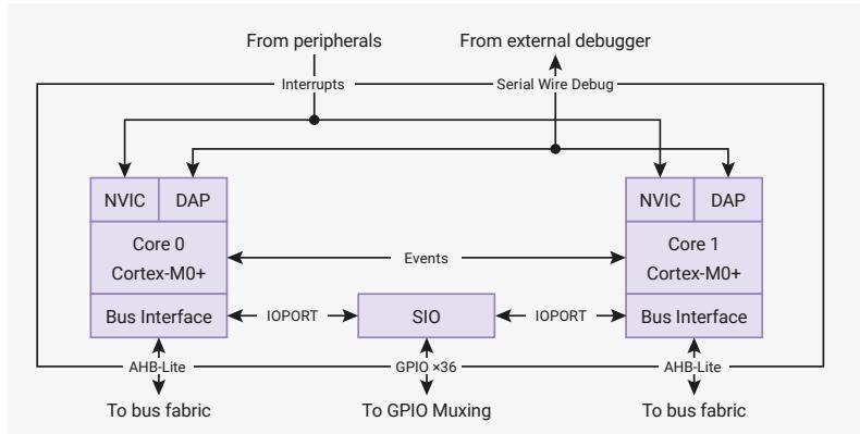
The RP2040 processor subsystem consists of two Arm Cortex-M0+ processors – each with its standard internal Arm CPU peripherals – alongside external peripherals for GPIO access and inter-core communication. Details of the Arm Cortex-M0+ processors, including the specific feature configuration used on RP2040, can be found in Section 2.4 .
Figure 6. Two Cortex-M0+ processors, each with a dedicated 32-bit AHB-Lite bus port, for code fetch, loads and stores. The SIO is connected to the single-cycle IOPORT bus of each processor, and provides GPIO access, two-way communications, and other core-local peripherals. Both processors can be debugged via a single multi-drop Serial Wire Debug bus. 26 interrupts (plus NMI) are routed to the NVIC and WIC on each processor.
i NOTE
The terms core0 and core1 , proc0 and proc1 are used interchangeably in RP2040's registers and documentation to refer to processor 0, and processor 1 respectively.
The processors use a number of interfaces to communicate with the rest of the system:
- • Each processor uses its own independent 32-bit AHB-Lite bus to access memory and memory-mapped peripherals (more detail in Section 2.1 )
- • The single-cycle IO block provides high-speed, deterministic access to GPIOs via each processor's IOPORT
- • 26 system-level interrupts are routed to both processors
- • A multi-drop Serial Wire Debug bus provides debug access to both processors from an external debug host
2.3.1. SIO
The Single-cycle IO block (SIO) contains several peripherals that require low-latency, deterministic access from the processors. It is accessed via each processor's IOPORT: this is an auxiliary bus port on the Cortex-M0+ which can perform rapid 32-bit reads and writes. The SIO has a dedicated bus interface for each processor's IOPORT, as shown in
Figure 7
. Processors access their IOPORT with normal load and store instructions, directed to the special IOPORT address segment,
0xd0000000...0xdfffffff
. The SIO appears as memory-mapped hardware within the IOPORT space.
i NOTE
The SIO is not connected to the main system bus due to its tight timing requirements. It can only be accessed by the processors, or by the debugger via the processor debug ports.
Figure 7. The single-cycle IO block contains memory-mapped hardware which the processors must be able to access quickly. The FIFOs and spinlocks support message passing and synchronisation between the two cores. The shared GPIO registers provide fast and concurrency-safe direct access to GPIO-capable pins. Some core-local arithmetic hardware can be used to accelerate common tasks on the processors.
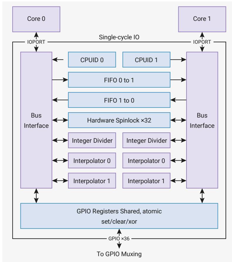
The diagram illustrates the single-cycle IO block architecture. Two cores, Core 0 and Core 1, are shown at the top, each connected to the system via an IOPORT. These IOPORTs connect to a central block labeled 'Single-cycle IO'. Inside this block, there are two 'Bus Interface' blocks, one for each core. Between these interfaces are several shared peripherals: 'CPUID 0' and 'CPUID 1' (each connected to its respective core interface), 'FIFO 0 to 1' and 'FIFO 1 to 0' (bidirectional), 'Hardware Spinlock x32', and three pairs of arithmetic units: 'Integer Divider', 'Interpolator 0', and 'Interpolator 1'. At the bottom of the central block is a large 'GPIO Registers Shared, atomic set/clear/xor' block. This block is connected to the bus interfaces and has a 'GPIO x36' output line leading to 'To GPIO Muxing'.
All IOPORT reads and writes (and therefore all SIO accesses) take place in exactly one cycle, unlike the main AHB-Lite system bus, where the Cortex-M0+ requires two cycles for a load or store, and may have to wait longer due to contention from other system bus masters. This is vital for interfaces such as GPIO, which have tight timing requirements.
SIO registers are mapped to word-aligned addresses in the range
0xd0000000...0xd000017c
. The remainder of the IOPORT space is reserved for future use.
The SIO peripherals are described in more detail in the following sections.
2.3.1.1. CPUID
The register
CPUID
is the first register in the IOPORT space. Core 0 reads a value of 0 when accessing this address, and core 1 reads a value of 1. This is a convenient method for software to determine on which core it is running. This is checked during the initial boot sequence: both cores start running simultaneously, core 1 goes into a deep sleep state, and core 0 continues with the main boot sequence.
! IMPORTANT
CPUID
should not be confused with the Cortex-M0+
CPUID
register (Section 2.4.4.1.1) on each processor's internal Private Peripheral Bus, which lists the processor's part number and version.
2.3.1.2. GPIO Control
The processors have access to GPIO registers for fast and direct control of pins with GPIO functionality. There are two identical sets of registers:
- • GPIO_x for direct control of IO bank 0 (user GPIOs 0 to 29, starting at the LSB)
- • GPIO_HI_x for direct control of the QSPI IO bank (in the order SCLK, SSn, SD0, SD1, SD2, SD3, starting at the LSB)
NOTE
To drive a pin with the SIO's GPIO registers, the GPIO multiplexer for this pin must first be configured to select the SIO GPIO function. See Table 279 .
These GPIO registers are shared between the two cores, and both cores can access them simultaneously. There are three registers for each bank:
- • Output registers, GPIO_OUT and GPIO_HI_OUT , are used to set the output level of the GPIO (1/0 for high/low)
- • Output enable registers, GPIO_OE and GPIO_HI_OE , are used to enable the output driver. 0 for high-impedance, 1 for drive high/low based on GPIO_OUT and GPIO_HI_OUT .
- • Input registers, GPIO_IN and GPIO_HI_IN , allow the processor to sample the current state of the GPIOs
Reading GPIO_IN returns all 30 GPIO values (or 6 for GPIO_HI_IN ) in a single read. Software can then mask out individual pins it is interested in.
SDK: https://github.com/raspberrypi/pico-sdk/blob/master/src/rp2_common/hardware_gpio/include/hardware/gpio.h Lines 859 - 869
859 static inline bool gpio_get(uint gpio) {
860     #ifdef NUM_BANK0_GPIOS <= 32
861         return sio_hw->gpio_in & (1u << gpio);
862     #else
863         if (gpio < 32) {
864             return sio_hw->gpio_in & (1u << gpio);
865         } else {
866             return sio_hw->gpio_hi_in & (1u << (gpio - 32));
867         }
868     #endif
869 }
The OUT and OE registers also have atomic SET, CLR, and XOR aliases, which allows software to update a subset of the pins in one operation. This is vital not only for safe parallel GPIO access between the two cores, but also safe concurrent GPIO access in an interrupt handler and foreground code running on one core.
SDK: https://github.com/raspberrypi/pico-sdk/blob/master/src/rp2_common/hardware_gpio/include/hardware/gpio.h Lines 908 - 914
908 static inline void gpio_set_mask(uint32_t mask) {
909     #ifdef PICO_USE_GPIO_COPROCESSOR
910         gpior_lo_out_set(mask);
911     #else
912         sio_hw->gpio_set = mask;
913     #endif
914 }
SDK: https://github.com/raspberrypi/pico-sdk/blob/master/src/rp2_common/hardware_gpio/include/hardware/gpio.h Lines 955 - 961
955 static inline void gpio_clr_mask(uint32_t mask) {
956     #ifdef PICO_USE_GPIO_COPROCESSOR
957         gpior_lo_out_clr(mask);
958     #else
959         sio_hw->gpio_clr = mask;
960     #endif
961 }
SDK: https://github.com/raspberrypi/pico-sdk/blob/master/src/rp2_common/hardware_gpio/include/hardware/gpio.h Lines 1145 - 1170
1145 static inline void gpio_put(uint gpio, bool value) {
1146 #ifdef PICO_USE_GPIO_COPROCESSOR
1147     gpioc_bit_out_put(gpio, value);
1148 #elif NUM_BANK0_GPIOS <= 32
1149     uint32_t mask = 1ul << gpio;
1150     if (value)
1151         gpio_set_mask(mask);
1152     else
1153         gpio_clr_mask(mask);
1154 #else
1155     uint32_t mask = 1ul << (gpio & 0x1fu);
1156     if (gpio < 32) {
1157         if (value) {
1158             sio_hw->gpio_set = mask;
1159         } else {
1160             sio_hw->gpio_clr = mask;
1161         }
1162     } else {
1163         if (value) {
1164             sio_hw->gpio_hi_set = mask;
1165         } else {
1166             sio_hw->gpio_hi_clr = mask;
1167         }
1168     }
1169 #endif
1170 }
If both processors write to an OUT or OE register (or any of its SET/CLR/XOR aliases) on the same clock cycle, the result is as though core 0 wrote first, and core 1 wrote immediately afterward. For example, if core 0 SETs a bit, and core 1 simultaneously XORs it, the bit will be set to 0, irrespective of its original value.
i NOTE
This is a conceptual model for the result that is produced when two cores write to a GPIO register simultaneously. The register does not actually contain this intermediate value at any point. In the previous example, if the pin is initially 0, and core 0 performs a SET while core 1 performs a XOR, the GPIO output remains low without any positive glitch.
2.3.1.3. Hardware Spinlocks
The SIO provides 32 hardware spinlocks, which can be used to manage mutually-exclusive access to shared software resources. Each spinlock is a one-bit flag, mapped to a different address (from SPINLOCK0 to SPINLOCK31 ). Software interacts with each spinlock with one of the following operations:
- • Read: attempt to claim the lock. Read value is nonzero if the lock was successfully claimed, or zero if the lock had already been claimed by a previous read.
- • Write (any value): release the lock. The next attempt to claim the lock will be successful.
If both cores try to claim the same lock on the same clock cycle, core 0 succeeds.
Generally software will acquire a lock by repeatedly polling the lock bit ("spinning" on the lock) until it is successfully claimed. This is inefficient if the lock is held for long periods, so generally the spinlocks should be used to protect the short critical sections of higher-level primitives such as mutexes, semaphores and queues.
For debugging purposes, the current state of all 32 spinlocks can be observed via SPINLOCK_ST .
2.3.1.4. Inter-processor FIFOs (Mailboxes)
The SIO contains two FIFOs for passing data, messages or ordered events between the two cores. Each FIFO is 32 bits wide, and eight entries deep. One of the FIFOs can only be written by core 0, and read by core 1. The other can only be written by core 1, and read by core 0.
Each core writes to its outgoing FIFO by writing to
FIFO_WR
, and reads from its incoming FIFO by reading from
FIFO_RD
. A status register,
FIFO_ST
, provides the following status signals:
- • Incoming FIFO contains data (
VLD) - • Outgoing FIFO has room for more data (
RDY) - • The incoming FIFO was read from while empty at some point in the past (
ROE) - • The outgoing FIFO was written to while full at some point in the past (
WOF)
Writing to the outgoing FIFO while full, or reading from the incoming FIFO while empty, does not affect the FIFO state. The current contents and level of the FIFO is preserved. However, this does represent some loss of data or reception of invalid data by the software accessing the FIFO, so a sticky error flag is raised (
ROE
or
WOF
).
The SIO has a FIFO IRQ output for each core, mapped to system IRQ numbers 15 and 16. Each IRQ output is the logical OR of the
VLD
,
ROE
and
WOF
bits in that core's
FIFO_ST
register: that is, the IRQ is asserted if any of these three bits is high, and clears again when they are all low. The
ROE
and
WOF
flags are cleared by writing any value to
FIFO_ST
, and the
VLD
flag is cleared by reading data from the FIFO until empty.
If the corresponding interrupt line is enabled in the Cortex-M0+ NVIC, then the processor will take an interrupt each time data appears in its FIFO, or if it has performed some invalid FIFO operation (read on empty, write on full). Typically Core 0 will use IRQ15 and core 1 will use IRQ16. If the IRQs are used the other way round then it is difficult for the core that has been interrupted to correctly identify the reason for the interrupt as the core doesn't have access to the other core's FIFO status register.
i NOTE
ROE
and
WOF
only become set if software misbehaves in some way. Generally, the interrupt handler will trigger when data appears in the FIFO (raising the
VLD
flag), and the interrupt handler clears the IRQ by reading data from the FIFO until
VLD
goes low once more.
The inter-processor FIFOs and the Cortex-M0+ Event signals are used by the bootrom (Section 2.8)
wait_for_vector
routine, where core 1 remains in a sleep state until it is woken, and provided with its initial stack pointer, entry point and vector table through the FIFO.
2.3.1.5. Integer Divider
The SIO provides one 8-cycle signed/unsigned divide/modulo module to each of the cores. Calculation is started by writing a dividend and divisor to the two argument registers,
DIVIDEND
and
DIVISOR
. The divider calculates the quotient / and remainder % of this division over the next 8 cycles, and on the 9th cycle the results can be read from the two result registers
DIV_QUOTIENT
and
DIV_REMAINDER
. A 'ready' bit in register
DIV_CSR
can be polled to wait for the calculation to complete, or software can insert a fixed 8-cycle delay.
SDK: https://github.com/raspberrypi/pico-sdk/blob/master/src/rp2_common/hardware_divider/divider.S Lines 12 - 16
12 regular_func_with_section hw_divider_divmod_s32
13     ldr r3, =(SIO_BASE)
14     str r0, [r3, #SIO_DIV_SDIVIDEND_OFFSET]
15     str r1, [r3, #SIO_DIV_SDIVISOR_OFFSET]
16     b hw_divider_divmod_return
Image: Note icon
NOTESoftware is free to perform other non-divider operations during these 8 cycles.
There are two aliases of the operand registers: writing to the signed alias ( DIV_SDIVIDEND and DIV_SDIVISOR ) will initiate a signed calculation, and the other ( DIV_UDIVIDEND and DIV_UDIVISOR ) will initiate an unsigned calculation.
SDK: https://github.com/raspberrypi/pico-sdk/blob/master/src/rp2_common/hardware_divider/divider.S Lines 20 - 24
20 regular_func_with_section hw_divider_divmod_u32
21     ldr r3, =(SIO_BASE)
22     str r0, [r3, #SIO_DIV_UDIVIDEND_OFFSET]
23     str r1, [r3, #SIO_DIV_UDIVISOR_OFFSET]
24     b hw_divider_divmod_return
Image: Note icon
NOTEA new calculation begins immediately with every write to an operand register, and a new operand write immediately squashes any calculation currently in progress. For example, when dividing many numbers by the same divisor, only xDIVISOR needs to be written, and the signedness of each calculation is determined by whether SDIVIDEND or UDIVIDEND is written.
To support save and restore on interrupt handler entry/exit (or on e.g. an RTOS context switch), the result registers are also writable. Writing to a result register will cancel any operation in progress at the time. The DIV_CSR.DIRTY flag can help make save/restore more efficient: this flag is set when any divider register (operand or result) is written to, and cleared when the quotient is read.
Image: Note icon
NOTEWhen enabled, the default divider AEABI support maps C level
/
and
%
to the hardware divider. When building software using the SDK and using the divider directly, it is important to read the quotient register
last
. This ensures the partial divider state will be correctly saved and restored by any interrupt code that uses the divider. You should read the quotient register whether you need the value or not.
The SDK module
pico_divider
https://github.com/raspberrypi/pico-sdk/blob/master/src/common/pico_divider_headers/include/pico/divider.h
provides both the AEABI implementation needed to hook the C
/
and
%
operators for both 32-bit and 64-bit integer division, as well as some additional C functions that return quotients and remainders at the same time. All of these functions correctly save and restore the hardware divider state (when dirty) so that they can be used in either user or IRQ handler code.
The SDK module
hardware_divider
https://github.com/raspberrypi/pico-sdk/blob/master/src/rp2_common/hardware_divider/include/hardware/divider.h
provides lower level macros and helper functions for accessing the hardware divider, but these do not save and restore the hardware divider state (although this header does provide separate functions to do so).
2.3.1.6. Interpolator
Each core is equipped with two interpolators ( INTERP0 and INTERP1 ) which can accelerate tasks by combining certain pre-configured operations into a single processor cycle. Intended for cases where the pre-configured operation is repeated many times, this results in code which uses both fewer CPU cycles and fewer CPU registers in the time-critical sections of the code.
The interpolators are used to accelerate audio operations within the SDK, but their flexible configuration makes it possible to optimise many other tasks such as quantization and dithering, table lookup address generation, affine texture mapping, decompression and linear feedback.
Figure 8. An interpolator. The two accumulator registers and three base registers have single-cycle read/write access from the processor. The interpolator is organised into two lanes, which perform masking, shifting and sign-extension operations on the two accumulators. This produces three possible results, by adding the intermediate shift/mask values to the three base registers. From left to right, the multiplexers on each lane are controlled by the following flags in the CTRL registers: CROSS_RESULT, CROSS_INPUT, SIGNED, ADD_RAW.
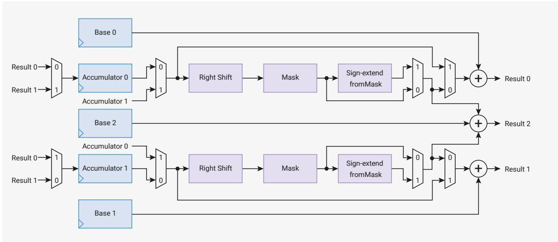
The processor can write or read any interpolator register in one cycle, and the results are ready on the next cycle. The processor can also perform an addition on one of the two accumulators
ACCUM0
or
ACCUM1
by writing to the corresponding
ACCUMx_ADD
register.
The three results are available in the read-only locations
PEEK0
,
PEEK1
,
PEEK2
. Reading from these locations does not change the state of the interpolator. The results are also aliased at the locations
POP0
,
POP1
,
POP2
; reading from a
POPx
alias returns the same result as the corresponding
PEEKx
, and simultaneously writes back the lane results to the accumulators. This can be used to advance the state of interpolator each time a result is read.
Additionally the interpolator supports simple fractional blending between two values as well as clamping values such that they lie within a given range.
The following example shows a trivial example of popping a lane result to produce simple iterative feedback.
Pico Examples: https://github.com/raspberrypi/pico-examples/blob/master/interp/hello_interp/hello_interp.c Lines 11 - 23
11 void times_table() {
12     puts("9 times table:");
13
14     // Initialise lane 0 on interp0 on this core
15     interp_config cfg = interp_default_config();
16     interp_set_config(interp0, 0, &cfg);
17
18     interp0->accum[0] = 0;
19     interp0->base[0] = 9;
20
21     for (int i = 0; i < 10; ++i)
22         printf("%d\n", interp0->pop[0]);
23 }
NOTE
By sheer coincidence, the interpolators are extremely well suited to SNES MODE7-style graphics routines. For example, on each core,
INTERP0
can provide a stream of tile lookups for some affine transform, and
INTERP1
can provide offsets into the tiles for the same transform.
2.3.1.6.1. Lane Operations
Figure 9. Each lane of each interpolator can be configured to perform mask, shift and sign-extension on one of the accumulators. This is fed into adders which produces final results, which may optionally be fed back into the accumulators with each read. The datapath can be configured using a handful of 32-bit multiplexers. From left to right, these are controlled by the following CTRL flags: CROSS_RESULT, CROSS_INPUT, SIGNED, ADD_RAW.

Each lane performs these three operations, in sequence:
- • A right shift by
CTRL_LANE
x
_SHIFT
(0 to 31 bits) - • A mask of bits from
CTRL_LANE x _MASK_LSBtoCTRL_LANE x _MASK_MSBinclusive (each ranging from bit 0 to bit 31) - • A sign extension from the top of the mask, i.e. take bit
CTRL_LANE x _MASK_MSBand OR it into all more-significant bits, ifCTRL_LANE x _SIGNEDis set
For example, if:
- •
ACCUM0 = 0xdeadbeef - •
CTRL_LANE0_SHIFT = 8 - •
CTRL_LANE0_MASK_LSB = 4 - •
CTRL_LANE0_MASK_MSB = 7 - •
CTRL_SIGNED = 1
Then lane 0 would produce the following results at each stage:
- • Right shift by 8 to produce
0x00deadbe - • Mask bits 7 to 4 to produce
0x00deadbe & 0x000000f0 = 0x000000b0 - • Sign-extend up from bit 7 to produce
0xffffffb0
In software:
Pico Examples: https://github.com/raspberrypi/pico-examples/blob/master/interp/hello_interp/hello_interp.c Lines 25 - 46
25 void moving_mask() {
26     interp_config cfg = interp_default_config();
27     interp0->accum[0] = 0x1234abcd;
28
29     puts("Masking:");
30     printf("ACCUM0 = %08x\n", interp0->accum[0]);
31     for (int i = 0; i < 8; ++i) {
32         // LSB, then MSB. These are inclusive, so 0,31 means "the entire 32 bit register"
33         interp_config_set_mask(&cfg, i * 4, i * 4 + 3);
34         interp_set_config(interp0, 0, &cfg);
35         // Reading from ACCUMx_ADD returns the raw lane shift and mask value, without BASEx
36         printf("Nibble %d: %08x\n", i, interp0->add_raw[0]);
37     }
38
39     puts("Masking with sign extension:");
40     interp_config_set_signed(&cfg, true);
41     for (int i = 0; i < 8; ++i) {
42         interp_config_set_mask(&cfg, i * 4, i * 4 + 3);
43         interp_set_config(interp0, 0, &cfg);
44         printf("Nibble %d: %08x\n", i, interp0->add_raw[0]);
45     }
46 }
The above example should print:
ACCUM0 = 1234abcd
Nibble 0: 0000000d
Nibble 1: 000000c0
Nibble 2: 00000b00
Nibble 3: 0000a000
Nibble 4: 00040000
Nibble 5: 00300000
Nibble 6: 02000000
Nibble 7: 10000000
Masking with sign extension:
Nibble 0: ffffffff
Nibble 1: ffffffff
Nibble 2: fffffb00
Nibble 3: fffa0000
Nibble 4: 00040000
Nibble 5: 00300000
Nibble 6: 02000000
Nibble 7: 10000000
Changing the result and input multiplexers can create feedback between the accumulators. This is useful e.g. for audio dithering.
Pico Examples: https://github.com/raspberrypi/pico-examples/blob/master/interp/hello_interp/hello_interp.c Lines 48 - 66
48 void cross_lanes() {
49     interp_config cfg = interp_default_config();
50     interp_config_set_cross_result(&cfg, true);
51     // ACCUM0 gets lane 1 result:
52     interp_set_config(interp0, 0, &cfg);
53     // ACCUM1 gets lane 0 result:
54     interp_set_config(interp0, 1, &cfg);
55
56     interp0->accum[0] = 123;
57     interp0->accum[1] = 456;
58     interp0->base[0] = 1;
59     interp0->base[1] = 0;
60     puts("Lane result crossover:");
61     for (int i = 0; i < 10; ++i) {
62         uint32_t peek0 = interp0->peek[0];
63         uint32_t pop1 = interp0->pop[1];
64         printf("PEEK0, POP1: %d, %d\n", peek0, pop1);
65     }
66 }
This should print:
PEEK0, POP1: 124, 456
PEEK0, POP1: 457, 124
PEEK0, POP1: 125, 457
PEEK0, POP1: 458, 125
PEEK0, POP1: 126, 458
PEEK0, POP1: 459, 126
PEEK0, POP1: 127, 459
PEEK0, POP1: 460, 127
PEEK0, POP1: 128, 460
PEEK0, POP1: 461, 128
2.3.1.6.2. Blend Mode
Blend mode is available on INTERP0 on each core, and is enabled by the CTRL_LANE0_BLEN0 control flag. It performs linear interpolation, which we define as follows:
Where \( x_0 \) is the register BASE0 , \( x_1 \) is the register BASE1 , and \( \alpha \) is a fractional value formed from the least significant 8 bits of the lane 1 shift and mask value.
Blend mode has the following differences from normal mode:
- • PEEK0, POP0 return the 8-bit alpha value (the 8 LSBs of the lane 1 shift and mask value), with zeroes in result bits 31 down to 24.
- • PEEK1, POP1 return the linear interpolation between BASE0 and BASE1
- • PEEK2, POP2 do not include lane 1 result in the addition (i.e. it is BASE2 + lane 0 shift and mask value)
The result of the linear interpolation is equal to BASE0 when the alpha value is 0, and equal to BASE0 + 255/256 * ( BASE1 - BASE0 ) when the alpha value is all-ones.
Pico Examples: https://github.com/raspberrypi/pico-examples/blob/master/interp/hello_interp/hello_interp.c Lines 68 - 87
68 void simple_blend1() {
69     puts("Simple blend 1:");
70
71     interp_config cfg = interp_default_config();
72     interp_config_set_blend(&cfg, true);
73     interp_set_config(interp0, 0, &cfg);
74
75     cfg = interp_default_config();
76     interp_set_config(interp0, 1, &cfg);
77
78     interp0->base[0] = 500;
79     interp0->base[1] = 1000;
80
81     for (int i = 0; i <= 6; i++) {
82         // set fraction to value between 0 and 255
83         interp0->accum[1] = 255 * i / 6;
84         // ≈ 500 + (1000 - 500) * i / 6;
85         printf("%d\n", (int) interp0->peek[1]);
86     }
87 }
This should print (note the 255/256 resulting in 998 not 1000):
500
582
666
748
832
914
998
CTRL_LANE1_SIGNED controls whether BASE0 and BASE1 are sign-extended for this interpolation (this sign extension is required because the interpolation produces an intermediate product value 40 bits in size). CTRL_LANE0_SIGNED continues to control the sign extension of the lane 0 intermediate result in PEEK2, POP2 as normal.
Pico Examples: https://github.com/raspberrypi/pico-examples/blob/master/interp/hello_interp/hello_interp.c Lines 90 - 121
90 void print_simple_blend2_results(bool is_signed) {
91     // lane 1 signed flag controls whether base 0/1 are treated as signed or unsigned
92     interp_config cfg = interp_default_config();
93     interp_config_set_signed(&cfg, is_signed);
94     interp_set_config(interp0, 1, &cfg);
95
96     for (int i = 0; i <= 6; i++) {
97         interp0->accum[1] = 255 * i / 6;
98         if (is_signed) {
99             printf("%d\n", (int) interp0->peek[1]);
100         } else {
101             printf("0x%08x\n", (uint) interp0->peek[1]);
102         }
103     }
104 }
105
106 void simple_blend2() {
107     puts("Simple blend 2:");
108
109     interp_config cfg = interp_default_config();
110     interp_config_set_blend(&cfg, true);
111     interp_set_config(interp0, 0, &cfg);
112
113     interp0->base[0] = (uint32_t) -1000;
114     interp0->base[1] = 1000;
115
116     puts("signed:");
117     print_simple_blend2_results(true);
118
119     puts("unsigned:");
120     print_simple_blend2_results(false);
121 }
This should print:
signed:
-1000
-672
-336
-8
328
656
992
unsigned:
0xffffffc18
0xd5fffd60
0xaaffffeb0
0x80fffff8
0x56000148
0x2c000290
0x010003e0
Finally, in blend mode when using the
BASE_1AND0
register to send a 16-bit value to each of
BASE0
and
BASE1
with a single 32-bit write, the sign-extension of these 16-bit values to full 32-bit values during the write is controlled by
CTRL_LANE1_SIGNED
for both bases, as opposed to non-blend-mode operation, where
CTRL_LANE0_SIGNED
affects extension into
BASE0
and
CTRL_LANE1_SIGNED
affects extension into
BASE1
.
Pico Examples: https://github.com/raspberrypi/pico-examples/blob/master/interp/hello_interp/hello_interp.c Lines 124 - 145
124 void simple_blend3() {
125     puts("Simple blend 3:");
126
127     interp_config cfg = interp_default_config();
128     interp_config_set_blend(&cfg, true);
129     interp_set_config(interp0, 0, &cfg);
130
131     cfg = interp_default_config();
132     interp_set_config(interp0, 1, &cfg);
133
134     interp0->accum[1] = 128;
135     interp0->base01 = 0x30005000;
136     printf("0x%08x\n", (int) interp0->peek[1]);
137     interp0->base01 = 0xe000f000;
138     printf("0x%08x\n", (int) interp0->peek[1]);
139
140     interp_config_set_signed(&cfg, true);
141     interp_set_config(interp0, 1, &cfg);
142
143     interp0->base01 = 0xe000f000;
144     printf("0x%08x\n", (int) interp0->peek[1]);
145 }
This should print:
0x00004000
0x0000e800
0xffffe800
2.3.1.6.3. Clamp Mode
Clamp mode is available on INTERP1 on each core, and is enabled by the CTRL_LANE0_CLAMP control flag. In clamp mode, the PEEK0/POP0 result is the lane value (shifted, masked, sign-extended ACCUM0 ) clamped between BASE0 and BASE1 . In other words, if the lane value is greater than BASE1 , a value of BASE1 is produced; if less than BASE0 , a value of BASE0 is produced; otherwise, the value passes through. No addition is performed. The signedness of these comparisons is controlled by the CTRL_LANE0_SIGNED flag.
Other than this, the interpolator behaves the same as in normal mode.
Pico Examples: https://github.com/raspberrypi/pico-examples/blob/master/interp/hello_interp/hello_interp.c Lines 193 - 211
193 void clamp() {
194     puts("Clamp:");
195     interp_config cfg = interp_default_config();
196     interp_config_set_clamp(&cfg, true);
197     interp_config_set_shift(&cfg, 2);
198     // set mask according to new position of sign bit..
199     interp_config_set_mask(&cfg, 0, 29);
200     // ...so that the shifted value is correctly sign extended
201     interp_config_set_signed(&cfg, true);
202     interp_set_config(interp1, 0, &cfg);
203
204     interp1->base[0] = 0;
205     interp1->base[1] = 255;
206
207     for (int i = -1024; i <= 1024; i += 256) {
208     interp1->accum[0] = i;
209     printf("%d\t%d\n", i, (int) interp1->peek[0]);
210 }
211 }
This should print:
-1024  0
-768   0
-512   0
-256   0
0       0
256    64
512    128
768    192
1024   255
2.3.1.6.4. Sample Use Case: Linear Interpolation
Linear interpolation is a more complete example of using blend mode in conjunction with other interpolator functionality:
In this example,
ACCUM0
is used to track a fixed point (integer/fraction) position within a list of values to be interpolated. Lane 0 is used to produce an address into the value array for the integer part of the position. The fractional part of the position is shifted to produce a value from 0-255 for the blend. The blend is performed between two consecutive values in the array.
Finally the fractional position is updated via a single write to
ACCUM0_ADD_RAW
.
Pico Examples: https://github.com/raspberrypi/pico-examples/blob/master/interp/hello_interp/hello_interp.c Lines 147 - 191
147 void linear_interpolation() {
148     puts("Linear interpolation:");
149     const int uv_fractional_bits = 12;
150
151     // for lane 0
152     // shift and mask XXXX XXXX XXXX XXXX XXXX FFFF FFFF FFFF (accum 0)
153     // to          0000 0000 000X XXXX XXXX XXXX XXXX XXX0
154     // i.e. non fractional part times 2 (for uint16_t)
155     interp_config cfg = interp_default_config();
156     interp_config_set_shift(&cfg, uv_fractional_bits - 1);
157     interp_config_set_mask(&cfg, 1, 32 - uv_fractional_bits);
158     interp_config_set_blend(&cfg, true);
159     interp_set_config(interp0, 0, &cfg);
160
161     // for lane 1
162     // shift XXXX XXXX XXXX XXXX XXXX FFFF FFFF FFFF (accum 0 via cross input)
163     // to      0000 XXXX XXXX XXXX XXXX FFFF FFFF FFFF
164
165     cfg = interp_default_config();
166     interp_config_set_shift(&cfg, uv_fractional_bits - 8);
167     interp_config_set_signed(&cfg, true);
168     interp_config_set_cross_input(&cfg, true); // signed blending
169     interp_set_config(interp0, 1, &cfg);
170
171     int16_t samples[] = {0, 10, -20, -1000, 500};
172
173     // step is 1/4 in our fractional representation
174     uint step = (1 << uv_fractional_bits) / 4;
175
176     interp0->accum[0] = 0; // initial sample_offset;
177     interp0->base[2] = (uintptr_t) samples;
178     for (int i = 0; i < 16; i++) {
179         // result2 = samples + (lane0 raw result)
180         // i.e. ptr to the first of two samples to blend between
181         int16_t *sample_pair = (int16_t *) interp0->peek[2];
182         interp0->base[0] = sample_pair[0];
183         interp0->base[1] = sample_pair[1];
184         uint32_t peek1 = interp0->peek[1];
185         uint32_t add_raw1 = interp0->add_raw[1];
186         printf("%d\t(%d%% between %d and %d)\n", (int) peek1,
187             100 * (add_raw1 & 0xff) / 0xff,
188             sample_pair[0], sample_pair[1]);
189         interp0->add_raw[0] = step;
190     }
191 }
This should print:
0      (0% between 0 and 10)
2      (25% between 0 and 10)
5      (50% between 0 and 10)
7      (75% between 0 and 10)
10     (0% between 10 and -20)
2      (25% between 10 and -20)
-5     (50% between 10 and -20)
-13    (75% between 10 and -20)
-20    (0% between -20 and -1000)
-265   (25% between -20 and -1000)
-510   (50% between -20 and -1000)
-755   (75% between -20 and -1000)
-1000  (0% between -1000 and 500)
-625   (25% between -1000 and 500)
-250   (50% between -1000 and 500)
125    (75% between -1000 and 500)
This method is used for fast approximate audio upscaling in the SDK
2.3.1.6.5. Sample Use Case: Simple Affine Texture Mapping
Simple affine texture mapping can be implemented by using fixed point arithmetic for texture coordinates, and stepping a fixed amount in each coordinate for every pixel in a scanline. The integer part of the texture coordinates are used to form an address within the texture to lookup a pixel colour.
By using two lanes, all three base values and the
CTRL_LANE
x
_ADD_RAW
flag, it is possible to reduce what would be quite an expensive CPU operation to a single cycle iteration using the interpolator.
Pico Examples: https://github.com/raspberrypi/pico-examples/blob/master/interp/hello_interp/hello_interp.c Lines 214 - 272
214 void texture_mapping_setup(uint8_t *texture, uint texture_width_bits, uint
    texture_height_bits,
215                          uint uv_fractional_bits) {
216     interp_config cfg = interp_default_config();
217     // set add_raw flag to use raw (un-shifted and un-masked) lane accumulator value when
    adding
218     // it to the lane base to make the lane result
219     interp_config_set_add_raw(&cfg, true);
220     interp_config_set_shift(&cfg, uv_fractional_bits);
221     interp_config_set_mask(&cfg, 0, texture_width_bits - 1);
222     interp_set_config(interp0, 0, &cfg);
223
224     interp_config_set_shift(&cfg, uv_fractional_bits - texture_width_bits);
225     interp_config_set_mask(&cfg, texture_width_bits, texture_width_bits +
texture_height_bits - 1);
226     interp_set_config(interp0, 1, &cfg);
227
228     interp0->base[2] = (uintptr_t) texture;
229 }
230
231 void texture_mapped_span(uint8_t *output, uint32_t u, uint32_t v, uint32_t du, uint32_t dv,
uint count) {
232     // u, v are texture coordinates in fixed point with uv_fractional_bits fractional bits
233     // du, dv are texture coordinate steps across the span in same fixed point.
234     interp0->accum[0] = u;
235     interp0->base[0] = du;
236     interp0->accum[1] = v;
237     interp0->base[1] = dv;
238     for (uint i = 0; i < count; i++) {
239         // equivalent to
240         // uint32_t sm_result0 = (accum0 >> uv_fractional_bits) & (1 << (texture_width_bits -
1);
241         // uint32_t sm_result1 = (accum1 >> uv_fractional_bits) & (1 << (texture_height_bits -
1);
242         // uint8_t *address = texture + sm_result0 + (sm_result1 << texture_width_bits);
243         // output[i] = *address;
244         // accum0 = du + accum0;
245         // accum1 = dv + accum1;
246
247         // result2 is the texture address for the current pixel;
248         // popping the result advances to the next iteration
249         output[i] = *(uint8_t *) interp0->pop[2];
250     }
251 }
252
253 void texture_mapping() {
254     puts("Affine Texture mapping (with texture wrap):");
255
256     uint8_t texture[] = {
257         0x00, 0x01, 0x02, 0x03,
258         0x10, 0x11, 0x12, 0x13,
259         0x20, 0x21, 0x22, 0x23,
260         0x30, 0x31, 0x32, 0x33,
261     };
262     // 4x4 texture
263     texture_mapping_setup(texture, 2, 2, 16);
264     uint8_t output[12];
265     uint32_t du = 65536 / 2; // step of 1/2
266     uint32_t dv = 65536 / 3; // step of 1/3
267     texture_mapped_span(output, 0, 0, du, dv, 12);
268
269     for (uint i = 0; i < 12; i++) {
270         printf("0x%02x\n", output[i]);
271     }
272 }
This should print:
0x00
0x00
0x01
0x01
0x12
0x12
0x13
0x23
0x20
0x20
0x31
0x31
2.3.1.7. List of Registers
The SIO registers start at a base address of
0xd0000000
(defined as
SIO_BASE
in SDK).
Table 16. List of SIO registers
| Offset | Name | Info |
|---|---|---|
| 0x000 | CPUID | Processor core identifier |
| 0x004 | GPIO_IN | Input value for GPIO pins |
| 0x008 | GPIO_HI_IN | Input value for QSPI pins |
| 0x010 | GPIO_OUT | GPIO output value |
| 0x014 | GPIO_OUT_SET | GPIO output value set |
| 0x018 | GPIO_OUT_CLR | GPIO output value clear |
| 0x01c | GPIO_OUT_XOR | GPIO output value XOR |
| 0x020 | GPIO_OE | GPIO output enable |
| 0x024 | GPIO_OE_SET | GPIO output enable set |
| 0x028 | GPIO_OE_CLR | GPIO output enable clear |
| 0x02c | GPIO_OE_XOR | GPIO output enable XOR |
| 0x030 | GPIO_HI_OUT | QSPI output value |
| 0x034 | GPIO_HI_OUT_SET | QSPI output value set |
| 0x038 | GPIO_HI_OUT_CLR | QSPI output value clear |
| 0x03c | GPIO_HI_OUT_XOR | QSPI output value XOR |
| 0x040 | GPIO_HI_OE | QSPI output enable |
| 0x044 | GPIO_HI_OE_SET | QSPI output enable set |
| 0x048 | GPIO_HI_OE_CLR | QSPI output enable clear |
| 0x04c | GPIO_HI_OE_XOR | QSPI output enable XOR |
| 0x050 | FIFO_ST | Status register for inter-core FIFOs (mailboxes). |
| 0x054 | FIFO_WR | Write access to this core's TX FIFO |
| 0x058 | FIFO_RD | Read access to this core's RX FIFO |
| 0x05c | SPINLOCK_ST | Spinlock state |
| 0x060 | DIV_UDIVIDEND | Divider unsigned dividend |
| Offset | Name | Info |
|---|---|---|
| 0x064 | DIV_UDIVISOR | Divider unsigned divisor |
| 0x068 | DIV_SDIVIDEND | Divider signed dividend |
| 0x06c | DIV_SDIVISOR | Divider signed divisor |
| 0x070 | DIV_QUOTIENT | Divider result quotient |
| 0x074 | DIV_REMAINDER | Divider result remainder |
| 0x078 | DIV_CSR | Control and status register for divider. |
| 0x080 | INTERP0_ACCUM0 | Read/write access to accumulator 0 |
| 0x084 | INTERP0_ACCUM1 | Read/write access to accumulator 1 |
| 0x088 | INTERP0_BASE0 | Read/write access to BASE0 register. |
| 0x08c | INTERP0_BASE1 | Read/write access to BASE1 register. |
| 0x090 | INTERP0_BASE2 | Read/write access to BASE2 register. |
| 0x094 | INTERP0_POP_LANE0 | Read LANE0 result, and simultaneously write lane results to both accumulators (POP). |
| 0x098 | INTERP0_POP_LANE1 | Read LANE1 result, and simultaneously write lane results to both accumulators (POP). |
| 0x09c | INTERP0_POP_FULL | Read FULL result, and simultaneously write lane results to both accumulators (POP). |
| 0x0a0 | INTERP0_PEEK_LANE0 | Read LANE0 result, without altering any internal state (PEEK). |
| 0x0a4 | INTERP0_PEEK_LANE1 | Read LANE1 result, without altering any internal state (PEEK). |
| 0x0a8 | INTERP0_PEEK_FULL | Read FULL result, without altering any internal state (PEEK). |
| 0x0ac | INTERP0_CTRL_LANE0 | Control register for lane 0 |
| 0x0b0 | INTERP0_CTRL_LANE1 | Control register for lane 1 |
| 0x0b4 | INTERP0_ACCUM0_ADD | Values written here are atomically added to ACCUM0 |
| 0x0b8 | INTERP0_ACCUM1_ADD | Values written here are atomically added to ACCUM1 |
| 0x0bc | INTERP0_BASE_1AND0 | On write, the lower 16 bits go to BASE0, upper bits to BASE1 simultaneously. |
| 0x0c0 | INTERP1_ACCUM0 | Read/write access to accumulator 0 |
| 0x0c4 | INTERP1_ACCUM1 | Read/write access to accumulator 1 |
| 0x0c8 | INTERP1_BASE0 | Read/write access to BASE0 register. |
| 0x0cc | INTERP1_BASE1 | Read/write access to BASE1 register. |
| 0x0d0 | INTERP1_BASE2 | Read/write access to BASE2 register. |
| 0x0d4 | INTERP1_POP_LANE0 | Read LANE0 result, and simultaneously write lane results to both accumulators (POP). |
| 0x0d8 | INTERP1_POP_LANE1 | Read LANE1 result, and simultaneously write lane results to both accumulators (POP). |
| 0x0dc | INTERP1_POP_FULL | Read FULL result, and simultaneously write lane results to both accumulators (POP). |
| 0x0e0 | INTERP1_PEEK_LANE0 | Read LANE0 result, without altering any internal state (PEEK). |
| Offset | Name | Info |
|---|---|---|
| 0x0e4 | INTERP1_PEEK_LANE1 | Read LANE1 result, without altering any internal state (PEEK). |
| 0x0e8 | INTERP1_PEEK_FULL | Read FULL result, without altering any internal state (PEEK). |
| 0x0ec | INTERP1_CTRL_LANE0 | Control register for lane 0 |
| 0x0f0 | INTERP1_CTRL_LANE1 | Control register for lane 1 |
| 0x0f4 | INTERP1_ACCUM0_ADD | Values written here are atomically added to ACCUM0 |
| 0x0f8 | INTERP1_ACCUM1_ADD | Values written here are atomically added to ACCUM1 |
| 0x0fc | INTERP1_BASE_1AND0 | On write, the lower 16 bits go to BASE0, upper bits to BASE1 simultaneously. |
| 0x100 | SPINLOCK0 | Spinlock register 0 |
| 0x104 | SPINLOCK1 | Spinlock register 1 |
| 0x108 | SPINLOCK2 | Spinlock register 2 |
| 0x10c | SPINLOCK3 | Spinlock register 3 |
| 0x110 | SPINLOCK4 | Spinlock register 4 |
| 0x114 | SPINLOCK5 | Spinlock register 5 |
| 0x118 | SPINLOCK6 | Spinlock register 6 |
| 0x11c | SPINLOCK7 | Spinlock register 7 |
| 0x120 | SPINLOCK8 | Spinlock register 8 |
| 0x124 | SPINLOCK9 | Spinlock register 9 |
| 0x128 | SPINLOCK10 | Spinlock register 10 |
| 0x12c | SPINLOCK11 | Spinlock register 11 |
| 0x130 | SPINLOCK12 | Spinlock register 12 |
| 0x134 | SPINLOCK13 | Spinlock register 13 |
| 0x138 | SPINLOCK14 | Spinlock register 14 |
| 0x13c | SPINLOCK15 | Spinlock register 15 |
| 0x140 | SPINLOCK16 | Spinlock register 16 |
| 0x144 | SPINLOCK17 | Spinlock register 17 |
| 0x148 | SPINLOCK18 | Spinlock register 18 |
| 0x14c | SPINLOCK19 | Spinlock register 19 |
| 0x150 | SPINLOCK20 | Spinlock register 20 |
| 0x154 | SPINLOCK21 | Spinlock register 21 |
| 0x158 | SPINLOCK22 | Spinlock register 22 |
| 0x15c | SPINLOCK23 | Spinlock register 23 |
| 0x160 | SPINLOCK24 | Spinlock register 24 |
| 0x164 | SPINLOCK25 | Spinlock register 25 |
| 0x168 | SPINLOCK26 | Spinlock register 26 |
| 0x16c | SPINLOCK27 | Spinlock register 27 |
| Offset | Name | Info |
|---|---|---|
| 0x170 | SPINLOCK28 | Spinlock register 28 |
| 0x174 | SPINLOCK29 | Spinlock register 29 |
| 0x178 | SPINLOCK30 | Spinlock register 30 |
| 0x17c | SPINLOCK31 | Spinlock register 31 |
SIO: CPUID Register
Offset: 0x000
Description
Processor core identifier
Table 17. CPUID Register
| Bits | Description | Type | Reset |
|---|---|---|---|
| 31:0 | Value is 0 when read from processor core 0, and 1 when read from processor core 1. | RO | - |
SIO: GPIO_IN Register
Offset: 0x004
Description
Input value for GPIO pins
Table 18. GPIO_IN Register
| Bits | Description | Type | Reset |
|---|---|---|---|
| 31:30 | Reserved. | - | - |
| 29:0 | Input value for GPIO0...29 | RO | 0x00000000 |
SIO: GPIO_HI_IN Register
Offset: 0x008
Description
Input value for QSPI pins
Table 19. GPIO_HI_IN Register
| Bits | Description | Type | Reset |
|---|---|---|---|
| 31:6 | Reserved. | - | - |
| 5:0 | Input value on QSPI IO in order 0..5: SCLK, SSn, SD0, SD1, SD2, SD3 | RO | 0x00 |
SIO: GPIO_OUT Register
Offset: 0x010
Description
GPIO output value
Table 20. GPIO_OUT Register
| Bits | Description | Type | Reset |
|---|---|---|---|
| 31:30 | Reserved. | - | - |
| Bits | Description | Type | Reset |
|---|---|---|---|
| 29:0 | Set output level (1/0 → high/low) for GPIO0...29. Reading back gives the last value written, NOT the input value from the pins. If core 0 and core 1 both write to GPIO_OUT simultaneously (or to a SET/CLR/XOR alias), the result is as though the write from core 0 took place first, and the write from core 1 was then applied to that intermediate result. | RW | 0x00000000 |
SIO: GPIO_OUT_SET Register
Offset: 0x014
Description
GPIO output value set
Table 21.
GPIO_OUT_SET
Register
| Bits | Description | Type | Reset |
|---|---|---|---|
| 31:30 | Reserved. | - | - |
| 29:0 | Perform an atomic bit-set on GPIO_OUT, i.e.
GPIO_OUT |= wdata | WO | 0x00000000 |
SIO: GPIO_OUT_CLR Register
Offset: 0x018
Description
GPIO output value clear
Table 22.
GPIO_OUT_CLR
Register
| Bits | Description | Type | Reset |
|---|---|---|---|
| 31:30 | Reserved. | - | - |
| 29:0 | Perform an atomic bit-clear on GPIO_OUT, i.e.
GPIO_OUT &= ~wdata | WO | 0x00000000 |
SIO: GPIO_OUT_XOR Register
Offset: 0x01c
Description
GPIO output value XOR
Table 23.
GPIO_OUT_XOR
Register
| Bits | Description | Type | Reset |
|---|---|---|---|
| 31:30 | Reserved. | - | - |
| 29:0 | Perform an atomic bitwise XOR on GPIO_OUT, i.e.
GPIO_OUT ^= wdata | WO | 0x00000000 |
SIO: GPIO_OE Register
Offset: 0x020
Description
GPIO output enable
Table 24. GPIO_OE
Register
| Bits | Description | Type | Reset |
|---|---|---|---|
| 31:30 | Reserved. | - | - |
| Bits | Description | Type | Reset |
|---|---|---|---|
| 29:0 | Set output enable (1/0 → output/input) for GPIO0...29. Reading back gives the last value written. If core 0 and core 1 both write to GPIO_OE simultaneously (or to a SET/CLR/XOR alias), the result is as though the write from core 0 took place first, and the write from core 1 was then applied to that intermediate result. | RW | 0x00000000 |
SIO: GPIO_OE_SET Register
Offset: 0x024
Description
GPIO output enable set
Table 25.
GPIO_OE_SET Register
| Bits | Description | Type | Reset |
|---|---|---|---|
| 31:30 | Reserved. | - | - |
| 29:0 | Perform an atomic bit-set on GPIO_OE, i.e. \( \text{GPIO\_OE} |= \text{wdata} \) | WO | 0x00000000 |
SIO: GPIO_OE_CLR Register
Offset: 0x028
Description
GPIO output enable clear
Table 26.
GPIO_OE_CLR Register
| Bits | Description | Type | Reset |
|---|---|---|---|
| 31:30 | Reserved. | - | - |
| 29:0 | Perform an atomic bit-clear on GPIO_OE, i.e. \( \text{GPIO\_OE} \&= \sim\text{wdata} \) | WO | 0x00000000 |
SIO: GPIO_OE_XOR Register
Offset: 0x02c
Description
GPIO output enable XOR
Table 27.
GPIO_OE_XOR
Register
| Bits | Description | Type | Reset |
|---|---|---|---|
| 31:30 | Reserved. | - | - |
| 29:0 | Perform an atomic bitwise XOR on GPIO_OE, i.e. \( \text{GPIO\_OE} \wedge= \text{wdata} \) | WO | 0x00000000 |
SIO: GPIO_HI_OUT Register
Offset: 0x030
Description
QSPI output value
Table 28.
GPIO_HI_OUT Register
| Bits | Description | Type | Reset |
|---|---|---|---|
| 31:6 | Reserved. | - | - |
| Bits | Description | Type | Reset |
|---|---|---|---|
| 5:0 | Set output level (1/0 → high/low) for QSPI IO0...5. Reading back gives the last value written, NOT the input value from the pins. If core 0 and core 1 both write to GPIO_HI_OUT simultaneously (or to a SET/CLR/XOR alias), the result is as though the write from core 0 took place first, and the write from core 1 was then applied to that intermediate result. | RW | 0x00 |
SIO: GPIO_HI_OUT_SET Register
Offset: 0x034
Description
QSPI output value set
Table 29.
GPIO_HI_OUT_SET
Register
| Bits | Description | Type | Reset |
|---|---|---|---|
| 31:6 | Reserved. | - | - |
| 5:0 | Perform an atomic bit-set on GPIO_HI_OUT, i.e.
GPIO_HI_OUT |= wdata | WO | 0x00 |
SIO: GPIO_HI_OUT_CLR Register
Offset: 0x038
Description
QSPI output value clear
Table 30.
GPIO_HI_OUT_CLR
Register
| Bits | Description | Type | Reset |
|---|---|---|---|
| 31:6 | Reserved. | - | - |
| 5:0 | Perform an atomic bit-clear on GPIO_HI_OUT, i.e.
GPIO_HI_OUT &= ~wdata | WO | 0x00 |
SIO: GPIO_HI_OUT_XOR Register
Offset: 0x03c
Description
QSPI output value XOR
Table 31.
GPIO_HI_OUT_XOR
Register
| Bits | Description | Type | Reset |
|---|---|---|---|
| 31:6 | Reserved. | - | - |
| 5:0 | Perform an atomic bitwise XOR on GPIO_HI_OUT, i.e.
GPIO_HI_OUT ^= wdata | WO | 0x00 |
SIO: GPIO_HI_OE Register
Offset: 0x040
Description
QSPI output enable
Table 32. GPIO_HI_OE
Register
| Bits | Description | Type | Reset |
|---|---|---|---|
| 31:6 | Reserved. | - | - |
| Bits | Description | Type | Reset |
|---|---|---|---|
| 5:0 | Set output enable (1/0 → output/input) for QSPI I00...5. Reading back gives the last value written. If core 0 and core 1 both write to GPIO_HI_OE simultaneously (or to a SET/CLR/XOR alias), the result is as though the write from core 0 took place first, and the write from core 1 was then applied to that intermediate result. | RW | 0x00 |
SIO: GPIO_HI_OE_SET Register
Offset: 0x044
Description
QSPI output enable set
Table 33.
GPIO_HI_OE_SET
Register
| Bits | Description | Type | Reset |
|---|---|---|---|
| 31:6 | Reserved. | - | - |
| 5:0 | Perform an atomic bit-set on GPIO_HI_OE, i.e.
GPIO_HI_OE |= wdata | WO | 0x00 |
SIO: GPIO_HI_OE_CLR Register
Offset: 0x048
Description
QSPI output enable clear
Table 34.
GPIO_HI_OE_CLR
Register
| Bits | Description | Type | Reset |
|---|---|---|---|
| 31:6 | Reserved. | - | - |
| 5:0 | Perform an atomic bit-clear on GPIO_HI_OE, i.e.
GPIO_HI_OE &= ~wdata | WO | 0x00 |
SIO: GPIO_HI_OE_XOR Register
Offset: 0x04c
Description
QSPI output enable XOR
Table 35.
GPIO_HI_OE_XOR
Register
| Bits | Description | Type | Reset |
|---|---|---|---|
| 31:6 | Reserved. | - | - |
| 5:0 | Perform an atomic bitwise XOR on GPIO_HI_OE, i.e.
GPIO_HI_OE ^= wdata | WO | 0x00 |
SIO: FIFO_ST Register
Offset: 0x050
Description
Status register for inter-core FIFOs (mailboxes).
There is one FIFO in the core 0 → core 1 direction, and one core 1 → core 0. Both are 32 bits wide and 8 words deep.
Core 0 can see the read side of the 1 → 0 FIFO (RX), and the write side of 0 → 1 FIFO (TX).
Core 1 can see the read side of the 0 → 1 FIFO (RX), and the write side of 1 → 0 FIFO (TX).
The SIO IRQ for each core is the logical OR of the VLD, WOF and ROE fields of its FIFO_ST register.
Table 36. FIFO_ST Register
| Bits | Description | Type | Reset |
|---|---|---|---|
| 31:4 | Reserved. | - | - |
| 3 | ROE : Sticky flag indicating the RX FIFO was read when empty. This read was ignored by the FIFO. | WC | 0x0 |
| 2 | WOF : Sticky flag indicating the TX FIFO was written when full. This write was ignored by the FIFO. | WC | 0x0 |
| 1 | RDY : Value is 1 if this core's TX FIFO is not full (i.e. if FIFO_WR is ready for more data) | RO | 0x1 |
| 0 | VLD : Value is 1 if this core's RX FIFO is not empty (i.e. if FIFO_RD is valid) | RO | 0x0 |
SIO: FIFO_WR Register
Offset: 0x054
Table 37. FIFO_WR Register
| Bits | Description | Type | Reset |
|---|---|---|---|
| 31:0 | Write access to this core's TX FIFO | WF | 0x00000000 |
SIO: FIFO_RD Register
Offset: 0x058
Table 38. FIFO_RD Register
| Bits | Description | Type | Reset |
|---|---|---|---|
| 31:0 | Read access to this core's RX FIFO | RF | - |
SIO: SPINLOCK_ST Register
Offset: 0x05c
Table 39. SPINLOCK_ST Register
| Bits | Description | Type | Reset |
|---|---|---|---|
| 31:0 | Spinlock state A bitmap containing the state of all 32 spinlocks (1=locked). Mainly intended for debugging. | RO | 0x00000000 |
SIO: DIV_UDIVIDEND Register
Offset: 0x060
Table 40. DIV_UDIVIDEND Register
| Bits | Description | Type | Reset |
|---|---|---|---|
| 31:0 | Divider unsigned dividend Write to the DIVIDEND operand of the divider, i.e. the p in \( p / q \) . Any operand write starts a new calculation. The results appear in QUOTIENT, REMAINDER. UDIVIDEND/SDIVIDEND are aliases of the same internal register. The U alias starts an unsigned calculation, and the S alias starts a signed calculation. | RW | 0x00000000 |
SIO: DIV_UDIVISOR Register
Offset: 0x064
Table 41.
DIV_UDIVISOR
Register
| Bits | Description | Type | Reset |
|---|---|---|---|
| 31:0 | Divider unsigned divisor Write to the DIVISOR operand of the divider, i.e. the q in \( p / q \) . Any operand write starts a new calculation. The results appear in QUOTIENT, REMAINDER. UDIVISOR/SDIVISOR are aliases of the same internal register. The U alias starts an unsigned calculation, and the S alias starts a signed calculation. | RW | 0x00000000 |
SIO: DIV_SDIVIDEND Register
Offset: 0x068
Table 42.
DIV_SDIVIDEND
Register
| Bits | Description | Type | Reset |
|---|---|---|---|
| 31:0 | Divider signed dividend The same as UDIVIDEND, but starts a signed calculation, rather than unsigned. | RW | 0x00000000 |
SIO: DIV_SDIVISOR Register
Offset: 0x06c
Table 43.
DIV_SDIVISOR
Register
| Bits | Description | Type | Reset |
|---|---|---|---|
| 31:0 | Divider signed divisor The same as UDIVISOR, but starts a signed calculation, rather than unsigned. | RW | 0x00000000 |
SIO: DIV_QUOTIENT Register
Offset: 0x070
Table 44.
DIV_QUOTIENT
Register
| Bits | Description | Type | Reset |
|---|---|---|---|
| 31:0 | Divider result quotient The result of \( DIVIDEND / DIVISOR \) (division). Contents undefined while CSR_READY is low. For signed calculations, QUOTIENT is negative when the signs of DIVIDEND and DIVISOR differ. This register can be written to directly, for context save/restore purposes. This halts any in-progress calculation and sets the CSR_READY and CSR_DIRTY flags. Reading from QUOTIENT clears the CSR_DIRTY flag, so should read results in the order REMAINDER, QUOTIENT if CSR_DIRTY is used. | RW | 0x00000000 |
SIO: DIV_REMAINDER Register
Offset: 0x074
Table 45.
DIV_REMAINDER
Register
| Bits | Description | Type | Reset |
|---|---|---|---|
| 31:0 | Divider result remainder The result of DIVIDEND % DIVISOR (modulo). Contents undefined while CSR_READY is low. For signed calculations, REMAINDER is negative only when DIVIDEND is negative. This register can be written to directly, for context save/restore purposes. This halts any in-progress calculation and sets the CSR_READY and CSR_DIRTY flags. | RW | 0x00000000 |
SIO: DIV_CSR Register
Offset: 0x078
Description
Control and status register for divider.
Table 46. DIV_CSR
Register
| Bits | Description | Type | Reset |
|---|---|---|---|
| 31:2 | Reserved. | - | - |
| 1 | DIRTY
: Changes to 1 when any register is written, and back to 0 when QUOTIENT is read. Software can use this flag to make save/restore more efficient (skip if not DIRTY). If the flag is used in this way, it's recommended to either read QUOTIENT only, or REMAINDER and then QUOTIENT, to prevent data loss on context switch. | RO | 0x0 |
| 0 | READY
: Reads as 0 when a calculation is in progress, 1 otherwise. Writing an operand (xDIVIDEND, xDIVISOR) will immediately start a new calculation, no matter if one is already in progress. Writing to a result register will immediately terminate any in-progress calculation and set the READY and DIRTY flags. | RO | 0x1 |
SIO: INTERP0_ACCUM0 Register
Offset: 0x080
Table 47.
INTERP0_ACCUM0
Register
| Bits | Description | Type | Reset |
|---|---|---|---|
| 31:0 | Read/write access to accumulator 0 | RW | 0x00000000 |
SIO: INTERP0_ACCUM1 Register
Offset: 0x084
Table 48.
INTERP0_ACCUM1
Register
| Bits | Description | Type | Reset |
|---|---|---|---|
| 31:0 | Read/write access to accumulator 1 | RW | 0x00000000 |
SIO: INTERP0_BASE0 Register
Offset: 0x088
Table 49.
INTERP0_BASE0
Register
| Bits | Description | Type | Reset |
|---|---|---|---|
| 31:0 | Read/write access to BASE0 register. | RW | 0x00000000 |
SIO: INTERP0_BASE1 Register
Offset: 0x08c
Table 50.
INTERP0_BASE1
Register
| Bits | Description | Type | Reset |
|---|---|---|---|
| 31:0 | Read/write access to BASE1 register. | RW | 0x00000000 |
SIO: INTERP0_BASE2 Register
Offset: 0x090
Table 51.
INTERP0_BASE2
Register
| Bits | Description | Type | Reset |
|---|---|---|---|
| 31:0 | Read/write access to BASE2 register. | RW | 0x00000000 |
SIO: INTERP0_POP_LANE0 Register
Offset: 0x094
Table 52.
INTERP0_POP_LANE0
Register
| Bits | Description | Type | Reset |
|---|---|---|---|
| 31:0 | Read LANE0 result, and simultaneously write lane results to both accumulators (POP). | RO | 0x00000000 |
SIO: INTERP0_POP_LANE1 Register
Offset: 0x098
Table 53.
INTERP0_POP_LANE1
Register
| Bits | Description | Type | Reset |
|---|---|---|---|
| 31:0 | Read LANE1 result, and simultaneously write lane results to both accumulators (POP). | RO | 0x00000000 |
SIO: INTERP0_POP_FULL Register
Offset: 0x09c
Table 54.
INTERP0_POP_FULL
Register
| Bits | Description | Type | Reset |
|---|---|---|---|
| 31:0 | Read FULL result, and simultaneously write lane results to both accumulators (POP). | RO | 0x00000000 |
SIO: INTERP0_PEEK_LANE0 Register
Offset: 0x0a0
Table 55.
INTERP0_PEEK_LANE
0 Register
| Bits | Description | Type | Reset |
|---|---|---|---|
| 31:0 | Read LANE0 result, without altering any internal state (PEEK). | RO | 0x00000000 |
SIO: INTERP0_PEEK_LANE1 Register
Offset: 0x0a4
Table 56.
INTERP0_PEEK_LANE
1 Register
| Bits | Description | Type | Reset |
|---|---|---|---|
| 31:0 | Read LANE1 result, without altering any internal state (PEEK). | RO | 0x00000000 |
SIO: INTERP0_PEEK_FULL Register
Offset: 0x0a8
Table 57.
INTERP0_PEEK_FULL
Register
| Bits | Description | Type | Reset |
|---|---|---|---|
| 31:0 | Read FULL result, without altering any internal state (PEEK). | RO | 0x00000000 |
SIO: INTERP0_CTRL_LANE0 Register
Offset: 0x0ac
Description
Control register for lane 0
Table 58.
INTERP0_CTRL_LANE
0 Register
| Bits | Description | Type | Reset |
|---|---|---|---|
| 31:26 | Reserved. | - | - |
| 25 | OVERF : Set if either OVERF0 or OVERF1 is set. | RO | 0x0 |
| 24 | OVERF1 : Indicates if any masked-off MSBs in ACCUM1 are set. | RO | 0x0 |
| 23 | OVERF0 : Indicates if any masked-off MSBs in ACCUM0 are set. | RO | 0x0 |
| 22 | Reserved. | - | - |
| 21 | BLEND
: Only present on INTERP0 on each core. If BLEND mode is enabled: - LANE1 result is a linear interpolation between BASE0 and BASE1, controlled by the 8 LSBs of lane 1 shift and mask value (a fractional number between 0 and 255/256ths) - LANE0 result does not have BASE0 added (yields only the 8 LSBs of lane 1 shift+mask value) - FULL result does not have lane 1 shift+mask value added (BASE2 + lane 0 shift+mask) LANE1 SIGNED flag controls whether the interpolation is signed or unsigned. | RW | 0x0 |
| 20:19 | FORCE_MSB
: ORed into bits 29:28 of the lane result presented to the processor on the bus. No effect on the internal 32-bit datapath. Handy for using a lane to generate sequence of pointers into flash or SRAM. | RW | 0x0 |
| 18 | ADD_RAW : If 1, mask + shift is bypassed for LANE0 result. This does not affect FULL result. | RW | 0x0 |
| 17 | CROSS_RESULT : If 1, feed the opposite lane's result into this lane's accumulator on POP. | RW | 0x0 |
| 16 | CROSS_INPUT
: If 1, feed the opposite lane's accumulator into this lane's shift + mask hardware. Takes effect even if ADD_RAW is set (the CROSS_INPUT mux is before the shift+mask bypass) | RW | 0x0 |
| 15 | SIGNED : If SIGNED is set, the shifted and masked accumulator value is sign-extended to 32 bits before adding to BASE0, and LANE0 PEEK/POP appear extended to 32 bits when read by processor. | RW | 0x0 |
| Bits 14:10 9:5 4:0 Bits | Description SHIFT Description | MASK_MSB : The most-significant bit allowed to pass by the mask (inclusive) MASK_LSB : The least-significant bit allowed to pass by the mask (inclusive) : Logical right-shift applied to accumulator before masking | Type RW RW RW Type | Reset 0x00 0x00 0x00 Reset |
|---|---|---|---|---|
| 1 Register 31:21 | Reserved. | - | - | |
| 20:19 | FORCE_MSB sequence | : ORed into bits 29:28 of the lane result presented to the processor on the bus. | RW | 0x0 |
| 18 | ADD_RAW | of pointers into flash or SRAM. : If 1, mask + shift is bypassed for LANE1 result. This does not affect FULL result. | RW | 0x0 |
| 17 | CROSS_RESULT | : If 1, feed the opposite lane’s result into this lane’s accumulator on POP. | RW | 0x0 |
| 16 | CROSS_INPUT | : If 1, feed the opposite lane’s accumulator into this lane’s shift + mask hardware. Takes effect even if ADD_RAW is set (the CROSS_INPUT mux is before the shift+mask bypass) | RW | 0x0 |
| 15 | SIGNED | : If SIGNED is set, the shifted and masked accumulator value is sign- extended to 32 bits before adding to BASE1, and LANE1 PEEK/POP appear extended to 32 bits when read by processor. | RW | 0x0 |
| 14:10 | MASK_MSB | : The most-significant bit allowed to pass by the mask (inclusive) Setting MSB < LSB may cause chip to turn inside-out | RW | 0x00 |
| 9:5 | MASK_LSB | : The least-significant bit allowed to pass by the mask (inclusive) | RW | 0x00 |
| 4:0 SIO | SHIFT | : Logical right-shift applied to accumulator before masking : INTERP0_ACCUM0_ADD Register | RW | 0x00 |
| Table 60. Offset Bits INTERP0_ACCUM0_AD | : 0x0b4 Description | Type | Reset | |
| D Register 31:24 | Reserved. | - | - | |
| 23:0 | Values written here are atomically added to ACCUM0 | RW | 0x000000 |
SIO: INTERP0_CTRL_LANE1 Register
Offset: 0x0b0
Description
Control register for lane 1
Table 59.
INTERP0_CTRL_LANE1 Register
SIO: INTERP0_ACCUM0_ADD Register
Offset: 0x0b4
Table 60.
INTERP0_ACCUM0_ADD Register
SIO: INTERP0_ACCUM1_ADD Register
Offset: 0x0b8
Table 61.
INTERP0_ACCUM1_AD
D Register
| Bits | Description | Type | Reset |
|---|---|---|---|
| 31:24 | Reserved. | - | - |
| 23:0 | Values written here are atomically added to ACCUM1 Reading yields lane 1's raw shift and mask value (BASE1 not added). | RW | 0x000000 |
SIO: INTERP0_BASE_1AND0 Register
Offset: 0x0bc
Table 62.
INTERP0_BASE_1AND
0 Register
| Bits | Description | Type | Reset |
|---|---|---|---|
| 31:0 | On write, the lower 16 bits go to BASE0, upper bits to BASE1 simultaneously. Each half is sign-extended to 32 bits if that lane's SIGNED flag is set. | WO | 0x00000000 |
SIO: INTERP1_ACCUM0 Register
Offset: 0x0c0
Table 63.
INTERP1_ACCUM0
Register
| Bits | Description | Type | Reset |
|---|---|---|---|
| 31:0 | Read/write access to accumulator 0 | RW | 0x00000000 |
SIO: INTERP1_ACCUM1 Register
Offset: 0x0c4
Table 64.
INTERP1_ACCUM1
Register
| Bits | Description | Type | Reset |
|---|---|---|---|
| 31:0 | Read/write access to accumulator 1 | RW | 0x00000000 |
SIO: INTERP1_BASE0 Register
Offset: 0x0c8
Table 65.
INTERP1_BASE0
Register
| Bits | Description | Type | Reset |
|---|---|---|---|
| 31:0 | Read/write access to BASE0 register. | RW | 0x00000000 |
SIO: INTERP1_BASE1 Register
Offset: 0x0cc
Table 66.
INTERP1_BASE1
Register
| Bits | Description | Type | Reset |
|---|---|---|---|
| 31:0 | Read/write access to BASE1 register. | RW | 0x00000000 |
SIO: INTERP1_BASE2 Register
Offset: 0x0d0
Table 67.
INTERP1_BASE2
Register
| Bits | Description | Type | Reset |
|---|---|---|---|
| 31:0 | Read/write access to BASE2 register. | RW | 0x00000000 |
SIO: INTERP1_POP_LANE0 Register
Offset: 0x0d4
Table 68.
INTERP1_POP_LANE0
Register
| Bits | Description | Type | Reset |
|---|---|---|---|
| 31:0 | Read LANE0 result, and simultaneously write lane results to both accumulators (POP). | RO | 0x00000000 |
SIO: INTERP1_POP_LANE1 Register
Offset: 0x0d8
Table 69.
INTERP1_POP_LANE1
Register
| Bits | Description | Type | Reset |
|---|---|---|---|
| 31:0 | Read LANE1 result, and simultaneously write lane results to both accumulators (POP). | RO | 0x00000000 |
SIO: INTERP1_POP_FULL Register
Offset: 0x0dc
Table 70.
INTERP1_POP_FULL
Register
| Bits | Description | Type | Reset |
|---|---|---|---|
| 31:0 | Read FULL result, and simultaneously write lane results to both accumulators (POP). | RO | 0x00000000 |
SIO: INTERP1_PEEK_LANE0 Register
Offset: 0x0e0
Table 71.
INTERP1_PEEK_LANE
0 Register
| Bits | Description | Type | Reset |
|---|---|---|---|
| 31:0 | Read LANE0 result, without altering any internal state (PEEK). | RO | 0x00000000 |
SIO: INTERP1_PEEK_LANE1 Register
Offset: 0x0e4
Table 72.
INTERP1_PEEK_LANE
1 Register
| Bits | Description | Type | Reset |
|---|---|---|---|
| 31:0 | Read LANE1 result, without altering any internal state (PEEK). | RO | 0x00000000 |
SIO: INTERP1_PEEK_FULL Register
Offset: 0x0e8
Table 73.
INTERP1_PEEK_FULL
Register
| Bits | Description | Type | Reset |
|---|---|---|---|
| 31:0 | Read FULL result, without altering any internal state (PEEK). | RO | 0x00000000 |
SIO: INTERP1_CTRL_LANE0 Register
Offset: 0x0ec
Description
Control register for lane 0
Table 74.
INTERP1_CTRL_LANE
0 Register
| Bits | Description | Type | Reset |
|---|---|---|---|
| 31:26 | Reserved. | - | - |
| 25 | OVERF : Set if either OVERF0 or OVERF1 is set. | RO | 0x0 |
| 24 | OVERF1 : Indicates if any masked-off MSBs in ACCUM1 are set. | RO | 0x0 |
| 23 | OVERF0 : Indicates if any masked-off MSBs in ACCUM0 are set. | RO | 0x0 |
| Bits 14:10 9:5 4:0 Bits | Description SHIFT Description | MASK_MSB : The most-significant bit allowed to pass by the mask (inclusive) MASK_LSB : The least-significant bit allowed to pass by the mask (inclusive) : Logical right-shift applied to accumulator before masking | Type RW RW RW Type | Reset 0x00 0x00 0x00 Reset |
|---|---|---|---|---|
| 21 | Reserved. | - | - | |
| 20:19 | FORCE_MSB sequence | : ORed into bits 29:28 of the lane result presented to the processor on the bus. | RW | 0x0 |
| 18 | ADD_RAW | of pointers into flash or SRAM. : If 1, mask + shift is bypassed for LANE0 result. This does not affect FULL result. | RW | 0x0 |
| 17 | CROSS_RESULT | : If 1, feed the opposite lane’s result into this lane’s accumulator on POP. | RW | 0x0 |
| 16 | CROSS_INPUT | : If 1, feed the opposite lane’s accumulator into this lane’s shift + mask hardware. Takes effect even if ADD_RAW is set (the CROSS_INPUT mux is before the shift+mask bypass) | RW | 0x0 |
| 15 | SIGNED | : If SIGNED is set, the shifted and masked accumulator value is sign- extended to 32 bits before adding to BASE0, and LANE0 PEEK/POP appear extended to 32 bits when read by processor. | RW | 0x0 |
| 14:10 | MASK_MSB | : The most-significant bit allowed to pass by the mask (inclusive) Setting MSB < LSB may cause chip to turn inside-out | RW | 0x00 |
| 9:5 | MASK_LSB | : The least-significant bit allowed to pass by the mask (inclusive) | RW | 0x00 |
| 4:0 SIO | SHIFT | : Logical right-shift applied to accumulator before masking : INTERP1_CTRL_LANE1 Register | RW | 0x00 |
| Table 75. Description Bits INTERP1_CTRL_LANE | Description | Type | Reset | |
| 1 Register 31:21 | Reserved. | - | - | |
| 20:19 | FORCE_MSB sequence | : ORed into bits 29:28 of the lane result presented to the processor on the bus. | RW | 0x0 |
| 18 | ADD_RAW | of pointers into flash or SRAM. : If 1, mask + shift is bypassed for LANE1 result. This does not affect FULL result. | RW | 0x0 |
| 17 | CROSS_RESULT | : If 1, feed the opposite lane’s result into this lane’s accumulator on POP. | RW | 0x0 |
SIO: INTERP1_CTRL_LANE1 Register
Offset: 0x0f0
Description
Control register for lane 1
Table 75.
INTERP1_CTRL_LANE1 Register
| Bits | Description | Type | Reset |
|---|---|---|---|
| 16 | CROSS_INPUT
: If 1, feed the opposite lane's accumulator into this lane's shift + mask hardware. Takes effect even if ADD_RAW is set (the CROSS_INPUT mux is before the shift+mask bypass) | RW | 0x0 |
| 15 | SIGNED : If SIGNED is set, the shifted and masked accumulator value is sign-extended to 32 bits before adding to BASE1, and LANE1 PEEK/POP appear extended to 32 bits when read by processor. | RW | 0x0 |
| 14:10 | MASK_MSB
: The most-significant bit allowed to pass by the mask (inclusive) Setting MSB < LSB may cause chip to turn inside-out | RW | 0x00 |
| 9:5 | MASK_LSB : The least-significant bit allowed to pass by the mask (inclusive) | RW | 0x00 |
| 4:0 | SHIFT : Logical right-shift applied to accumulator before masking | RW | 0x00 |
SIO: INTERP1_ACCUM0_ADD Register
Offset: 0x0f4
Table 76.
INTERP1_ACCUM0_ADD
Register
| Bits | Description | Type | Reset |
|---|---|---|---|
| 31:24 | Reserved. | - | - |
| 23:0 | Values written here are atomically added to ACCUM0 Reading yields lane 0's raw shift and mask value (BASE0 not added). | RW | 0x000000 |
SIO: INTERP1_ACCUM1_ADD Register
Offset: 0x0f8
Table 77.
INTERP1_ACCUM1_ADD
Register
| Bits | Description | Type | Reset |
|---|---|---|---|
| 31:24 | Reserved. | - | - |
| 23:0 | Values written here are atomically added to ACCUM1 Reading yields lane 1's raw shift and mask value (BASE1 not added). | RW | 0x000000 |
SIO: INTERP1_BASE_1AND0 Register
Offset: 0x0fc
Table 78.
INTERP1_BASE_1AND
0 Register
| Bits | Description | Type | Reset |
|---|---|---|---|
| 31:0 | On write, the lower 16 bits go to BASE0, upper bits to BASE1 simultaneously. Each half is sign-extended to 32 bits if that lane's SIGNED flag is set. | WO | 0x00000000 |
SIO: SPINLOCK0, SPINLOCK1, ..., SPINLOCK30, SPINLOCK31 Registers
Offsets: 0x100, 0x104, ..., 0x178, 0x17c
Table 79. SPINLOCK0,
SPINLOCK1, ...,
SPINLOCK30,
SPINLOCK31
Registers
| Bits | Description | Type | Reset |
|---|---|---|---|
| 31:0 | Reading from a spinlock address will:
Writing (any value) releases the lock. If core 0 and core 1 attempt to claim the same lock simultaneously, core 0 wins. The value returned on success is \( 0x1 \ll \text{lock number} \) . | RW | 0x00000000 |
2.3.2. Interrupts
Each core is equipped with a standard ARM Nested Vectored Interrupt Controller (NVIC) which has 32 interrupt inputs. Each NVIC has the same interrupts routed to it, with the exception of the GPIO interrupts: there is one GPIO interrupt per bank, per core. These are completely independent, so e.g. core 0 can be interrupted by GPIO 0 in bank 0, and core 1 by GPIO 1 in the same bank.
On RP2040, only the lower 26 IRQ signals are connected on the NVIC, and IRQs 26 to 31 are tied to zero (never firing). The core can still be forced to enter the relevant interrupt handler by writing bits 26 to 31 in the NVIC ISPR register.
Table 80. Interrupts
| IRQ | Interrupt Source | IRQ | Interrupt Source | IRQ | Interrupt Source | IRQ | Interrupt Source | IRQ | Interrupt Source |
|---|---|---|---|---|---|---|---|---|---|
| 0 | TIMER_IRQ_0 | 6 | XIP_IRQ | 12 | DMA_IRQ_1 | 18 | SPI0_IRQ | 24 | I2C1_IRQ |
| 1 | TIMER_IRQ_1 | 7 | PIO0_IRQ_0 | 13 | IO_IRQ_BANK0 | 19 | SPI1_IRQ | 25 | RTC_IRQ |
| 2 | TIMER_IRQ_2 | 8 | PIO0_IRQ_1 | 14 | IO_IRQ_QSPI | 20 | UART0_IRQ | ||
| 3 | TIMER_IRQ_3 | 9 | PIO1_IRQ_0 | 15 | SIO_IRQ_PROC0 | 21 | UART1_IRQ | ||
| 4 | PWM_IRQ_WRAP | 10 | PIO1_IRQ_1 | 16 | SIO_IRQ_PROC1 | 22 | ADC_IRQ_FIFO | ||
| 5 | USBCTRL_IRQ | 11 | DMA_IRQ_0 | 17 | CLOCKS_IRQ | 23 | I2C0_IRQ |
i NOTE
XIP_IRQ is from the SSI block that makes up part of the XIP block. It could be used in a configuration where code is running from SRAM instead of flash. In this configuration, the XIP block could be used as a normal SSI peripheral.
Nested interrupts are supported in hardware: a lower-priority interrupt can be preempted by a higher-priority interrupt (or another exception e.g. HardFault), and the lower-priority interrupt will resume once higher-priority exceptions have completed. The priority order is determined by:
- • First, the dynamic priority level configured per interrupt by the NVIC_IPR0-7 registers. The Cortex-M0+ implements the two most significant bits of an 8-bit priority field, so four priority levels are available, and the numerically-lowest level (level 0) is the highest priority.
- • Second, for interrupts with the same dynamic priority level, the lower-numbered IRQ has higher priority (using the IRQ numbers given in the table above).
Some care has gone into arranging the RP2040 interrupt table to give a sensible default priority ordering, but individual interrupts can be raised or lowered in priority, using NVIC_IPR0 through NVIC_IPR7 , to suit a particular use case.
The 26 system IRQ signals are masked (NMI mask) and then ORed together creating the NMI signal for the core. The NMI mask for each core can be configured using PROC0_NMI_MASK and PROC1_NMI_MASK in the Syscfg register block. Each of these registers has one bit for each system interrupt, and the each core's NMI is asserted if a system interrupt is asserted and the corresponding NMI mask bit is set for that core.
⚠ CAUTIONIf the watchdog is armed, and some bits are set on the core 1 NMI mask, the RESETS block (and hence Syscfg) should be included in the watchdog reset list. Otherwise, following a watchdog event, core 1 NMI may be asserted when the core enter the bootrom. It is safe for core 0 to take an NMI when entering the bootrom (the handler will clear the NMI mask).
2.3.3. Event Signals
The Cortex-M0+ can enter a sleep state until an "event" (or interrupt) takes place, using the WFE instruction. It can also generate events, using the SEV instruction. On RP2040 the event signals are cross-wired between the two processors, so that an event sent by one processor will be received on the other.
i NOTEThe event flag is "sticky", so if both processors send an event ( SEV ) simultaneously, and then both go to sleep ( WFE ), they will both wake immediately, rather than getting stuck in a sleep state.
While in a WFE (or WFI ) sleep state, the processor can shut off its internal clock gates, consuming much less power. When both processors are sleeping, and the DMA is inactive, RP2040 as a whole can enter a sleep state, disabling clocks on unused infrastructure such as the busfabric, and waking automatically when one of the processors wakes. See Section 2.11.2 .
2.3.4. Debug
The 2-wire Serial Wire Debug (SWD) port provides access to hardware and software debug features including:
- • Loading firmware into SRAM or external flash memory
- • Control of processor execution: run/halt, step, set breakpoints, other standard Arm debug functionality
- • Access to processor architectural state
- • Access to memory and memory-mapped IO via the system bus
The SWD bus is exposed on two dedicated pins and is immediately available after power-on.
i NOTEWe recommend a max SWD frequency of 24MHz. This depends heavily on your setup. You may need to run much slower (1MHz) depending on the quality and length of your cables.
Debug access is via independent DAPs (one per core) attached to a shared multidrop SWD bus (SWD v2). Each DAP will only respond to debug commands if correctly addressed by a SWD TARGETSEL command; all others tristate their outputs. Additionally, a Rescue DP (see Section 2.3.4.2 ) is available which is connected to system control features. Default addresses of each debug port are given below:
- • Core 0: 0x01002927
- • Core 1: 0x11002927
- • Rescue DP: 0xf1002927
The Instance IDs (top 4 bits of ID above) can be changed via a sysconfig register which may be useful in a multichip application. However note that ID=0xf is reserved for the internal Rescue DP (see Section 2.3.4.2 ).
Figure 10. RP2040 Debugging
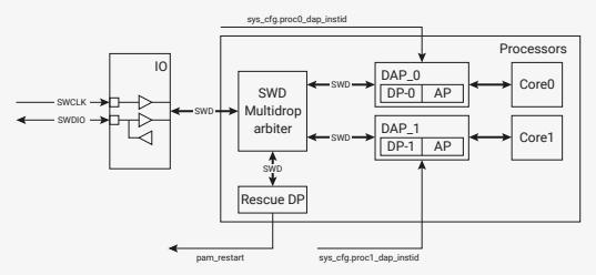
2.3.4.1. Software control of SWD pins
The SWD pins for Core 0 and Core 1 can be bit-banged via registers in syscfg (see DBGFORCE ). This means that Core 1 could run a USB application that allows debug of Core 0, or similar.
2.3.4.2. Rescue DP
The Rescue DP (debug port) is available over the SWD bus and is only intended for use in the specific case where the chip has locked up, for example if code has been programmed into flash which permanently halts the system clock: in such a case, the normal debugger can not communicate with the processors to return the system to a working state, so more drastic action is needed. A rescue is invoked by setting the CDBGPWRUPREQ bit in the Rescue DP’s CTRL/STAT register.
This causes a hard reset of the chip (functionally similar to a power-on-reset), and sets a flag in the Chip Level Reset block to indicate that a rescue reset took place. The bootrom checks this flag almost immediately in the initial boot process (before watchdog, flash or USB boot), acknowledges by clearing the bit, then halts the processor. This leaves the system in a safe state, with the system clock running, so that the debugger can reattach to the cores and load fresh code.
For a practical example of using the Rescue DP, see the Hardware design with RP2040 book.
2.4. Cortex-M0+
ARM Documentation
Excerpted from the Cortex-M0+ Technical Reference Manual . Used with permission.
The ARM Cortex-M0+ processor is a very low gate count, highly energy efficient processor that is intended for microcontroller and deeply embedded applications that require an area optimized, low-power processor.
2.4.1. Features
The ARM Cortex-M0+ processor features and benefits are:
- • Tight integration of system peripherals reduces area and development costs.
- • Thumb instruction set combines high code density with 32-bit performance.
- • Support for single-cycle I/O access.
- • Power control optimization of system components.
- • Integrated sleep modes for low-power consumption.
- • Fast code execution enables running the processor with a slower clock or increasing sleep mode time.
- • Optimized code fetching for reduced flash and ROM power consumption.
- • Hardware multiplier.
- • Deterministic, high-performance interrupt handling for time-critical applications.
- • Deterministic instruction cycle timing.
- • Support for system level debug authentication.
- • Serial Wire Debug reduces the number of pins required for debugging.
2.4.1.1. Interfaces
The interfaces included in the processor for external access include:
- • External AHB-Lite interface to busfabric
- • Debug Access Port (DAP)
- • Single-cycle I/O Port to SIO peripherals
2.4.1.2. Configuration
Each processor is configured with the following features:
- • Architectural clock gating (for power saving)
- • Little Endian bus access
- • Four Breakpoints
- • Debug support (via 2-wire debug pins SWD/SWCLK )
- • 32-bit instruction fetch (to match 32-bit data bus)
- • IOPORT (for low latency access to local peripherals (see SIO ))
- • 26 interrupts
- • 8 MPU regions
- • All registers reset on powerup
- • Fast multiplier (MULS 32×32 single cycle)
- • SysTick timer
- • Vector Table Offset Register ( VTOR )
- • 34 WIC (Wake-up Interrupt Controller) lines (32 IRQ and NMI, RXEV)
- • DAP feature: Halt event support
- • DAP feature: SerialWire debug interface (protocol 2 with multidrop support)
- • DAP feature: Micro Trace Buffer (MTB) is not implemented
Architectural clock gating allows the processor core to support SLEEP and DEEPSLEEP power states by disabling the clock to parts of the processor core. Note that power gating is not supported.
Each M0+ core has its own interrupt controller which can individually mask out interrupt sources as required. The same interrupts are routed to both M0+ cores.
2.4.1.3. ARM architecture
The processor implements the ARMv6-M architecture profile. See the ARMv6-M Architecture Reference Manual , and for
further details refer to the ARM Cortex M0+ Technical Reference Manual .
2.4.2. Functional Description
2.4.2.1. Overview
The Cortex-M0+ processor is a configurable, multistage, 32-bit RISC processor. It has an AMBA AHB-Lite interface and includes an NVIC component. It also has hardware debug, single-cycle I/O interfacing, and memory-protection functionality. The processor can execute Thumb code and is compatible with other Cortex-M profile processors.
Figure 11 shows the functional blocks of the processor and surrounding blocks.
Figure 11. Cortex M0+ Functional block diagram
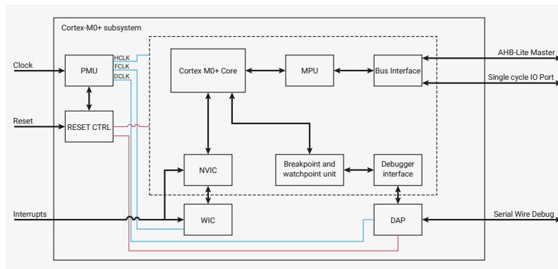
2.4.2.2. Features
The M0+ features:
- • The ARMv6-M Thumb® instruction set.
- • Thumb-2 technology.
- • An ARMv6-M compliant 24-bit SysTick timer.
- • A 32-bit hardware multiplier. This is the standard single-cycle multiplier
- • The ability to have deterministic, fixed-latency, interrupt handling.
- • Load/store multiple instructions that can be abandoned and restarted to facilitate rapid interrupt handling.
- • C Application Binary Interface compliant exception model. This is the ARMv6-M, C Application Binary Interface (C-ABI) compliant exception model that enables the use of pure C functions as interrupt handlers.
- • Low power sleep-mode entry using Wait For Interrupt (WFI), Wait For Event (WFE) instructions, or the return from interrupt sleep-on-exit feature.
2.4.2.3. NVIC features
The Nested Vectored Interrupt Controller (NVIC) features are:
- • 26 external interrupt inputs, each with four levels of priority.
- • Dedicated Non-Maskable Interrupt (NMI) input (which can be driven from any standard interrupt source)
- • Support for both level-sensitive and pulse-sensitive interrupt lines.
- • Wake-up Interrupt Controller (WIC), providing ultra-low power sleep mode support.
- • Relocatable vector table.
The NVIC supports hardware nesting of exceptions, e.g. an interrupt handler may itself be interrupted if a higher-priority interrupt request arrives whilst the handler is running.
Further details available in Section 2.4.5 .
2.4.2.4. Debug features
Debug features are:
- • Four hardware breakpoints.
- • Two watchpoints.
- • Program Counter Sampling Register (PCSR) for non-intrusive code profiling.
- • Single step and vector catch capabilities.
- • Support for unlimited software breakpoints using BKPT instruction.
- • Non-intrusive access to core peripherals and zero-waitstate system slaves through a compact bus matrix. A debugger can access these devices, including memory, even when the processor is running.
- • Full access to core registers when the processor is halted.
- • CoreSight compliant debug access through a Debug Access Port (DAP) supporting Serial Wire debug connections.
2.4.2.4.1. Debug Access Port
The processor is implemented with a low gate count Debug Access Port (DAP). The low gate count Debug Access Port (DAP) provides a Serial Wire debug-port, and connects to the processor slave port to provide full system-level debug access. For more information on DAP, see the ADI v5.1 version of the ARM Debug Interface v5, Architecture Specification
2.4.2.5. MPU features
Memory Protection Unit (MPU) features are:
- • Eight user-configurable memory regions.
- • Eight sub-region disables per region.
- • Execute never (XN) support.
- • Default memory map support.
Further details available in Section 2.4.6 .
2.4.2.6. AHB-Lite interface
Transactions on the AHB-Lite interface are always marked as non-sequential. Processor accesses and debug accesses share the external interface to external AHB peripherals. The processor accesses take priority over debug accesses. Any vendor-specific components can populate this bus.
NOTEInstructions are only fetched using the AHB-Lite interface. To optimize performance, the Cortex-M0+ processor fetches ahead of the instruction it is executing. To minimize power consumption, the fetch ahead is limited to a maximum of 32 bits.
2.4.2.7. Single-cycle I/O port
The processor implements a single-cycle I/O port that provides high speed access to tightly-coupled peripherals, such as general-purpose-I/O (GPIO). The port is accessible both by loads and stores from either the processor or the debugger. You cannot execute code from the I/O port.
2.4.2.8. Power Management Unit
Each processor has its own Power Management Unit (PMU) which allows power saving by turning off clocks to parts of the processor core. There are no separate power domains on RP2040.
The PMU runs from the processor clock which is controlled from the chip level clocks block. The PMU can control the following clock domains within the processor:
- • A debug clock containing the processor debug resources and the rest of the DAP.
- • A system clock containing the NVIC.
- • A processor clock containing the core and associated interfaces
Control is limited to clock enable/disable. When enabled, all domains run at the same clock speed.
The PMU also interfaces with the WIC, to ensure that power-down and wake-up behaviours are transparent to software and work with clocking and sleeping requirements. This includes SLEEP or DEEPSLEEP support as controlled in SCR register.
2.4.2.8.1. Power Management
RP2040 ARM Cortex M0+ uses ARMv6-M which supports the use of Wait For Interrupt ( WFI ) and Wait For Event ( WFE ) instructions as part of system power management:
WFI provides a mechanism for hardware support of entry to one or more sleep states. Hardware can suspend execution until a wakeup event occurs.
WFE provides a mechanism for software to suspend program execution until a wakeup condition occurs with minimal or no impact on wakeup latency. Both WFI and WFE are hint instructions that might have no effect on program execution. Normally, they are used in software idle loops that resume program execution only after an interrupt or event of interest occurs.
NOTECode using WFE and WFI must handle any spurious wakeup events caused by a debug halt or other reasons.
Refer to the SDK and ARMv6-M guide for further information.
2.4.2.8.2. Wait For Event and Send Event
RP2040 can support software-based synchronization to system events using the Send-Event ( SEV ) and WFE hint instructions. Software can:
- • use the WFE instruction to indicate that it is able to suspend execution of a process or thread until an event occurs, permitting hardware to enter a low power state.
- • rely on a mechanism that is transparent to software and provides low latency wakeup.
The WFE mechanism relies on hardware and software working together to achieve energy saving. For example, stalling execution of a processor until a device or another processor has set a flag:
- • the hardware provides the mechanism to enter the WFE low-power state.
- • software enters a polling loop to determine when the flag is set:
- • the polling processor issues a WFE instruction as part of a polling loop if the flag is clear.
- • an event is generated (hardware interrupt or Send-Event instruction from another processor) when the flag is set.
WFE wake up events
The following events are WFE wake up events:
- • the execution of an SEV instruction on the other processor
- • any exception entering the pending state if SEVONPEND in the System Control Register is set to 1.
- • an asynchronous exception at a priority that preempts any currently active exceptions.
- • a debug event with debug enabled.
The Event Register
The Event Register is a single bit register. When set, an Event Register indicates that an event has occurred, since the register was last cleared, that might prevent the processor having to suspend operation on issuing a WFE instruction. The following conditions apply to the Event Register:
- • A reset clears the Event Register.
- • Any WFE wakeup event, or the execution of an exception return instruction, sets the Event Register.
- • A WFE instruction clears the Event Register.
- • Software cannot read or write the value of the Event Register directly.
The Send-Event instruction
The Send-Event ( SEV ) instruction causes an event to be signalled to the other processor. The Send-Event instruction generates a wakeup event.
The Wait For Event instruction
The action of the WFE instruction depends on the state of the Event Register:
- • If the Event Register is set, the instruction clears the register and returns immediately.
- • If the Event Register is clear the processor can suspend execution and enter a low-power state. It can remain in that state until the processor detects a WFE wakeup event or a reset. When the processor detects a WFE wakeup event, the WFE instruction completes.
WFE wakeup events can occur before a WFE instruction is issued. Software using the WFE mechanism must tolerate spurious wake up events, including multiple wakeups.
2.4.2.8.3. Wait For Interrupt
RP2040 supports Wait For Interrupt through the hint instruction, WFI .
When a processor issues a WFI instruction it can suspend execution and enter a low-power state. It can remain in that state until the processor detects one of the following WFI wake up events:
- • A reset.
- • An asynchronous exception at a priority that, if PRIMASK.PM was set to 0, would preempt any currently active exceptions.
If
PRIMASK.PM
is set to 1, an asynchronous exception that has a higher group priority than any active exception results in a
WFI
instruction exit. If the group priority of the exception is less than or equal to the execution group priority, the exception is ignored.
- • If debug is enabled, a debug event.
- • A
WFIwakeup event.
The
WFI
instruction completes when the hardware detects a WFI wake up event.
The processor recognizes WFI wake up events only after issuing the
WFI
instruction.
2.4.2.8.4. Wakeup Interrupt Controller
The Wakeup Interrupt Controller (WIC) is used to wake the processor from a DEEPSLEEP state as controlled by the
SCR
register. In a DEEPSLEEP state clocks to the processor core and NVIC are not running. It can take a few cycles to wake from a DEEPSLEEP state.
The WIC takes inputs from the receive event signal (from the other processor), 32 interrupts lines, and NMI.
For more power saving, RP2040 supports system level power saving modes as defined in Section 2.11 which also includes code examples.
2.4.2.9. Reset Control
The Cortex M0+ Reset Control block controls the following resets:
- • Debug reset
- • M0+ core reset
- • PMU reset
After power up, both processors are released from reset (see details in Section 2.13.2 ). This releases reset to Debug, M0+ core and PMU.
Once running, resets can be triggered from the Debugger, NVIC (using
AIRCR.SYSRESETREQ
), or the RP2040 Power On State Machine controller (see details in
Section 2.13
). The NVIC only resets the Cortex-M0+ processor core (not the Debug or PMU), whereas the Power On State Machine controller can reset the processor subsystem which asserts all resets in the subsystem (Debug, M0+ core, PMU).
2.4.3. Programmer's model
2.4.3.1. About the programmer's model
The ARMv6-M Architecture Reference Manual provides a complete description of the programmer's model. This chapter gives an overview of the Cortex-M0+ programmer's model that describes the implementation-defined options. It also contains the ARMv6-M Thumb instructions it uses and their cycle counts for the processor. Additional details are in following chapters
- • Section 2.4.4 summarizes the system control features of the programmer's model.
- • Section 2.4.5 summarizes the NVIC features of the programmer's model.
- • Section 2.3.4 summarizes the Debug features of the programmer's model.
2.4.3.2. Modes of operation and execution
See the ARMv6-M Architecture Reference Manual for information about the modes of operation and execution.
2.4.3.3. Instruction set summary
The processor implements the ARMv6-M Thumb instruction set, including a number of 32-bit instructions that use Thumb-2 technology. The ARMv6-M instruction set comprises:
- • All of the 16-bit Thumb instructions from ARMv7-M excluding CBZ, CBNZ and IT.
- • The 32-bit Thumb instructions BL, DMB, DSB, ISB, MRS and MSR.
Table 81 shows the Cortex-M0+ instructions and their cycle counts. The cycle counts are based on a system with zero wait-states.
Table 81. Cortex-M0+ instruction summary
| Operation | Description | Assembler | Cycles |
|---|---|---|---|
| Move | 8-bit immediate | MOVS Rd, #<imm> | 1 |
| Lo to Lo | MOVS Rd, Rm | 1 | |
| Any to Any | MOV Rd, Rm | 1 | |
| Any to PC | MOV PC, Rm | 2 | |
| Add | 3-bit immediate | ADDS Rd, Rn, #<imm> | 1 |
| All registers Lo | ADDS Rd, Rn, Rm | 1 | |
| Any to Any | ADD Rd, Rd, Rm | 1 | |
| Any to PC | ADD PC, PC, Rm | 2 | |
| 8-bit immediate | ADDS Rd, Rd, #<imm> | 1 | |
| With carry | ADCS Rd, Rd, Rm | 1 | |
| Immediate to SP | ADD SP, SP, #<imm> | 1 | |
| Form address from SP | ADD Rd, SP, #<imm> | 1 | |
| Form address from PC | ADR Rd, <label> | 1 | |
| Subtract | SUBS Rd, Rn, Rm | 1 | |
| 3-bit immediate | SUBS Rd, Rn, #<imm> | 1 | |
| 8-bit immediate | SUBS Rd, Rd, #<imm> | 1 | |
| Subtract | With carry | SBCS Rd, Rd, Rm | 1 |
| Immediate from SP | SUB SP, SP, #<imm> | 1 | |
| Negate | RSBS Rd, Rn, #0 | 1 | |
| Multiply | MULS Rd, Rm, Rd | 1 | |
| Compare | CMP Rn, Rm | 1 | |
| Negative | CMN Rn, Rm | 1 | |
| Logical | Immediate | CMP Rn, #<imm> | 1 |
| AND | ANDS Rd, Rd, Rm | 1 | |
| Exclusive OR | EORS Rd, Rd, Rm | 1 | |
| OR | ORRS Rd, Rd, Rm | 1 |
| Operation | Description | Assembler | Cycles |
|---|---|---|---|
| Bit clear | BICS Rd, Rd, Rm | 1 | |
| Move NOT | MVNS Rd, Rm | 1 | |
| AND test | TST Rn, Rm | 1 | |
| Shift | Logical shift left by immediate | LSLS Rd, Rm, #<shift> | 1 |
| Logical shift left by register | LSLS Rd, Rd, Rs | 1 | |
| Logical shift right by immediate | LSRS Rd, Rm, #<shift> | 1 | |
| Logical shift right by register | LSRS Rd, Rd, Rs | 1 | |
| Arithmetic shift right | ASRS Rd, Rm, #<shift> | 1 | |
| Arithmetic shift right by register | ASRS Rd, Rd, Rs | 1 | |
| Rotate | Rotate right by register | RORS Rd, Rd, Rs | 1 |
| Load | Word, immediate offset | LDR Rd, [Rn, #<imm>] | 2 or 1 a |
| Halfword, immediate offset | LDRH Rd, [Rn, #<imm>] | 2 or 1 a | |
| Byte, immediate offset | LDRB Rd, [Rn, #<imm>] | 2 or 1 a | |
| Word, register offset | LDR Rd, [Rn, Rm] | 2 or 1 a | |
| Halfword, register offset | LDRH Rd, [Rn, Rm] | 2 or 1 a | |
| Signed halfword, register offset | LDRSH Rd, [Rn, Rm] | 2 or 1 a | |
| Byte, register offset | LDRB Rd, [Rn, Rm] | 2 or 1 a | |
| Signed byte, register offset | LDRSB Rd, [Rn, Rm] | 2 or 1 a | |
| PC-relative | LDR Rd, <label> | 2 or 1 a | |
| SP-relative | LDR Rd, [SP, #<imm>] | 2 or 1 a | |
| Multiple, excluding base | LDM Rn!, {<loreglist>} | 1+N b | |
| Multiple, including base | LDM Rn, {<loreglist>} | 1+N b | |
| Store | Word, immediate offset | STR Rd, [Rn, #<imm>] | 2 or 1 a |
| Halfword, immediate offset | STRH Rd, [Rn, #<imm>] | 2 or 1 a | |
| Byte, immediate offset | STRB Rd, [Rn, #<imm>] | 2 or 1 a | |
| Word, register offset | STR Rd, [Rn, Rm] | 2 or 1 a | |
| Halfword, register offset | STRH Rd, [Rn, Rm] | 2 or 1 a | |
| Byte, register offset | STRB Rd, [Rn, Rm] | 2 or 1 a | |
| SP-relative | STR Rd, [SP, #<imm>] | 2 or 1 a | |
| Multiple | STM Rn!, {<loreglist>} | 1+N b | |
| Push | Push | PUSH {<loreglist>} | 1+N b |
| Push with link register | PUSH {<loreglist>, LR} | 1+N c | |
| Pop | Pop | POP {<loreglist>} | 1+N b |
| Pop and return | POP {<loreglist>, PC} | 3+N c | |
| Branch | Conditional | B<cc> <label> | 1 or 2 d |
| Unconditional | B <label> | 2 |
| Operation | Description | Assembler | Cycles |
|---|---|---|---|
| With link | BL <label> | 3 | |
| With exchange | BX Rm | 2 | |
| With link and exchange | BLX Rm | 2 | |
| Extend | Signed halfword to word | SXTH Rd, Rm | 1 |
| Signed byte to word | SXTB Rd, Rm | 1 | |
| Unsigned halfword | UXTH Rd, Rm | 1 | |
| Unsigned byte | UXTB Rd, Rm | 1 | |
| Reverse | Bytes in word | REV Rd, Rm | 1 |
| Bytes in both halfwords | REV16 Rd, Rm | 1 | |
| Signed bottom half word | REVSH Rd, Rm | 1 | |
| State | change Supervisor Call | SVC #<imm> | - e |
| Disable interrupts | CPSID i | 1 | |
| Enable interrupts | CPSIE i | 1 | |
| Read special register | MRS Rd, <specreg> | 3 | |
| Write special register | MSR <specreg>, Rn | 3 | |
| Breakpoint | BKPT #<imm> | - e | |
| Hint | Send-Event | SEV | 1 |
| Wait For Event | WFE | 2 f | |
| Wait For Interrupt | WFI | 2 f | |
| Yield | YIELD | 1 f | |
| No operation | NOP | 1 | |
| Barriers | Instruction synchronization | ISB | 3 |
| Data memory | DMB | 3 | |
| Data synchronization | DSB | 3 |
Table Notes
- a 2 if to AHB interface or SCS, 1 if to single-cycle I/O port.
- b N is the number of elements in the list.
- c N is the number of elements in the list including PC or LR.
- d 2 if taken, 1 if not-taken.
- e Cycle count depends on processor and debug configuration.
- f Excludes time spent waiting for an interrupt or event.
- g Executes as NOP.
See the ARMv6-M Architecture Reference Manual for more information about the ARMv6-M Thumb instructions.
2.4.3.4. Memory model
The processor contains a bus matrix that arbitrates the processor core and Debug Access Port (DAP) memory accesses to both the external memory system and to the internal NVIC and debug components.
Priority is always given to the processor to ensure that any debug accesses are as non-intrusive as possible. For a zero
wait-state system, all debug accesses to system memory, NVIC, and debug resources are completely non-intrusive for typical code execution.
The system memory map is ARMv6-M architecture compliant, and is common both to the debugger and processor accesses. Transactions are routed as follows:
- • All accesses below 0xd0000000 or above 0xffffffff appear as AHB-Lite transactions on the AHB-Lite master port of the processor.
- • Accesses in the range 0xd0000000 to 0xdfffffff are handled by the SIO.
- • Accesses in the range 0xe0000000 to 0xffffffff are handled within the processor and do not appear on the AHB-Lite master port of the processor.
The processor supports only word size accesses in the range 0xd0000000 - 0xffffffff.
Table 82 shows the code, data, and device suitability for each region of the default memory map. This is the memory map used by implementations when the MPU is disabled. The attributes and permissions of all regions, except that targeting the Cortex-M0+ NVIC and debug components, can be modified using an implemented MPU.
Table 82. M0+ Default memory map usage
| Address range | Code | Data | Device |
|---|---|---|---|
| 0xf0000000 - 0xffffffff | No | No | Yes |
| 0xe0000000 - 0xffffffff | No | No | No a |
| 0xa0000000 - 0xdfffffff | No | No | Yes |
| 0x60000000 - 0x9fffffff | Yes | Yes | No |
| 0x40000000 - 0x5fffffff | No | No | Yes |
| 0x20000000 - 0x3fffffff | Yes | Yes | No |
| 0x00000000 - 0x1fffffff | Yes | Yes | No |
a . Space reserved for Cortex-M0+ NVIC and debug components.
Note
Regions not marked as suitable for code behave as eXecute-Never (XN) and generate a HardFault exception if code attempts to execute from this location.
See the ARMv6-M Architecture Reference Manual for more information about the memory model.
2.4.3.5. Processor core registers summary
Table 83 shows the processor core register set summary. Each of these registers is 32 bits wide.
Table 83. M0+ processor core register set summary
| Name | Description |
|---|---|
| R0-R12 | R0-R12 are general-purpose registers for data operations. |
| MSP/PSP (R13) | The Stack Pointer (SP) is register R13. In Thread mode, the CONTROL register indicates the stack pointer to use, Main Stack Pointer (MSP) or Process Stack Pointer (PSP). |
| LR (R14) | The Link Register (LR) is register R14. It stores the return information for subroutines, function calls, and exceptions. |
| PC (R15) | The Program Counter (PC) is register R15. It contains the current program address. |
| Name | Description |
|---|---|
| PSR | The Program Status Register (PSR) combines:
These registers provide different views of the PSR. |
| PRIMASK | The PRIMASK register prevents activation of all exceptions with configurable priority. |
| CONTROL | The CONTROL register controls the stack used, the code privilege level, when the processor is in Thread mode. |
See the ARMv6-M Architecture Reference Manual for information about the processor core registers and their addresses, access types, and reset values.
2.4.3.6. ExceptionsThis section describes the exception model of the processor.
2.4.3.6.1. Exception handlingThe processor implements advanced exception and interrupt handling, as described in the ARMv6-M Architecture Reference Manual. To minimize interrupt latency, the processor abandons any load-multiple or store-multiple instruction to take any pending interrupt. On return from the interrupt handler, the processor restarts the load-multiple or store-multiple instruction from the beginning.
This means that software must not use load-multiple or store-multiple instructions when a device is accessed in a memory region that is read-sensitive or sensitive to repeated writes. The software must not use these instructions in any case where repeated reads or writes might cause inconsistent results or unwanted side-effects.
The processor implementation can ensure that a fixed number of cycles are required for the NVIC to detect an interrupt signal and the processor fetch the first instruction of the associated interrupt handler. If this is done, the highest priority interrupt is jitter-free. This will depend on where the interrupt handler is located and if another higher priority master is accessing that memory. SRAM4 and SRAM5 are provided that may be allocated to interrupt handlers for each processor so this is jitter-free.
To reduce interrupt latency and jitter, the Cortex-M0+ processor implements both interrupt late-arrival and interrupt tail-chaining mechanisms, as defined by the ARMv6-M architecture. The worst case interrupt latency, for the highest priority active interrupt in a zero wait-state system not using jitter suppression, is 15 cycles.
The processor exception model has the following implementation-defined behaviour in addition to the architecture specified behaviour:
- • Exceptions on stacking from HardFault to NMI lockup at NMI priority.
- • Exceptions on unstacking from NMI to HardFault lockup at HardFault priority.
2.4.4.1. System control register summary
Table 84 gives the system control registers. Each of these registers is 32 bits wide.
Table 84. M0+ System control registers
| Name | Description |
|---|---|
| SYST_CSR | SysTick Control and Status Register |
| SYST_RVR | SysTick Reload Value Register |
| SYST_CVR | SysTick Current Value Register |
| SYST_CALIB | SysTick Calibration value Register |
| CPUID | See CPUID Register |
| ICSR | Interrupt Control State Register |
| AIRCR | Application Interrupt and Reset Control Register |
| CCR | Configuration and Control Register |
| SHPR2 | System Handler Priority Register |
| SHPR3 | System Handler Priority Register |
| SHCSR | System Handler Control and State Register |
| VTOR | Vector table Offset Register |
| ACTLR | Auxiliary Control Register |
Note
- • All system control registers are only accessible using word transfers. Any attempt to read or write a halfword or byte is Unpredictable.
- • See the List of Registers or ARMv6-M Architecture Reference Manual for more information about the system control registers, and their addresses and access types, and reset values.
2.4.4.1.1. CPUID Register
The CPUID contains the part number, version, and implementation information that is specific to the processor.
 IMPORTANT
This standard internal Arm register contains information about the type of processor. It should not be confused with CPUID (Section 2.3.1.1), an RP2040 SIO register which reads as 0 on core 0 and 1 on core 1.
2.4.5. NVIC
2.4.5.1. About the NVIC
External interrupt signals connect to the Nested Vectored Interrupt Controller (NVIC), and the NVIC prioritizes the interrupts. Software can set the priority of each interrupt. The NVIC and the Cortex-M0+ processor core are closely coupled, providing low latency interrupt processing and efficient processing of late arriving interrupts.
NOTE
"Nested" refers to the fact that interrupts can themselves be interrupted, by higher-priority interrupts. "Vectored" refers to the hardware dispatching each interrupt to a distinct handler routine, specified by the vector table. Details of nesting and vectoring behaviour are given in the ARMv6-M Architecture Reference Manual.
All NVIC registers are only accessible using word transfers. Any attempt to read or write a halfword or byte individually is unpredictable.
NVIC registers are always little-endian.
Processor exception handling is described in Exceptions section.
2.4.5.1.1. SysTick timer
A 24-bit SysTick system timer, extends the functionality of both the processor and the NVIC and provides:
- • A 24-bit system timer (SysTick).
- • Additional configurable priority SysTick interrupt.
The SysTick timer uses a 1µs pulse as a clock enable. This is generated in the watchdog block as timer_tick. Accuracy of SysTick timing depends upon accuracy of this timer_tick. The SysTick timer can also run from the system clock (see SYST_CALIB ).
See the ARMv6-M Architecture Reference Manual for more information.
2.4.5.1.2. Low power modes
The implementation includes a WIC. This enables the processor and NVIC to be put into a very low-power sleep mode leaving the WIC to identify and prioritize interrupts.
The processor fully implements the Wait For Interrupt (WFI), Wait For Event (WFE) and the Send Event (SEV) instructions. In addition, the processor also supports the use of SLEEPONEXIT, that causes the processor core to enter sleep mode when it returns from an exception handler to Thread mode. See the ARMv6-M Architecture Reference Manual for more information.
2.4.5.2. NVIC register summary
Table 85 shows the NVIC registers. Each of these registers is 32 bits wide.
Table 85. M0+ NVIC registers
| Name | Description |
|---|---|
| NVIC_ISER | Interrupt Set-Enable Register. |
| NVIC_ICER | Interrupt Clear-Enable Register. |
| NVIC_ISPR | Interrupt Set-Pending Register. |
| NVIC_ICPR | Interrupt Clear-Pending Register. |
| NVIC_IPR0 - NVIC_IPR7 | Interrupt Priority Registers. |
Note
See the List of Registers or ARMv6-M Architecture Reference Manual for more information about the NVIC registers and their addresses, access types, and reset values.
2.4.6. MPU
2.4.6.1. About the MPU
The MPU is a component for memory protection which allows the processor to support the ARMv6 Protected Memory System Architecture model. The MPU provides full support for:
- • Eight unified protection regions.
- • Overlapping protection regions, with ascending region priority:
- ◦ 7 = highest priority.
- ◦ 0 = lowest priority.
- • Access permissions.
- • Exporting memory attributes to the system.
MPU mismatches and permission violations invoke the HardFault handler. See the ARMv6-M Architecture Reference Manual for more information.
You can use the MPU to:
- • Enforce privilege rules.
- • Separate processes.
- • Manage memory attributes.
2.4.6.2. MPU register summary
Table 86 shows the MPU registers. Each of these registers is 32 bits wide.
Table 86. M0+ MPU registers
| Name | Description |
|---|---|
| MPU_TYPE | MPU Type Register. |
| MPU_CTRL | MPU Control Register. |
| MPU_RNR | MPU Region Number Register. |
| MPU_RBAR | MPU Region Base Address Register. |
| MPU_RASR | MPU Region Attribute and Size Register. |
Note
- • See the ARMv6-M Architecture Reference Manual for more information about the MPU registers and their addresses, access types, and reset values.
- • The MPU supports region sizes from 256-bytes to 4Gb, with 8-sub regions per region.
2.4.7. Debug
Basic debug functionality includes processor halt, single-step, processor core register access, Reset and HardFault Vector Catch, unlimited software breakpoints, and full system memory access. See the ARMv6-M Architecture Reference Manual.
The debug features for this device are:
- • A breakpoint unit supporting 4 hardware breakpoints.
- • A watchpoint unit supporting 2 watchpoints.
2.4.8. List of Registers
The ARM Cortex-M0+ registers start at a base address of
0xe0000000
(defined as
PPB_BASE
in SDK).
Table 87. List of M0PLUS registers
| Offset | Name | Info |
|---|---|---|
| 0xe010 | SYST_CSR | SysTick Control and Status Register |
| 0xe014 | SYST_RVR | SysTick Reload Value Register |
| 0xe018 | SYST_CVR | SysTick Current Value Register |
| 0xe01c | SYST_CALIB | SysTick Calibration Value Register |
| 0xe100 | NVIC_ISER | Interrupt Set-Enable Register |
| 0xe180 | NVIC_ICER | Interrupt Clear-Enable Register |
| 0xe200 | NVIC_ISPR | Interrupt Set-Pending Register |
| 0xe280 | NVIC_ICPR | Interrupt Clear-Pending Register |
| 0xe400 | NVIC_IPR0 | Interrupt Priority Register 0 |
| 0xe404 | NVIC_IPR1 | Interrupt Priority Register 1 |
| 0xe408 | NVIC_IPR2 | Interrupt Priority Register 2 |
| 0xe40c | NVIC_IPR3 | Interrupt Priority Register 3 |
| 0xe410 | NVIC_IPR4 | Interrupt Priority Register 4 |
| 0xe414 | NVIC_IPR5 | Interrupt Priority Register 5 |
| 0xe418 | NVIC_IPR6 | Interrupt Priority Register 6 |
| 0xe41c | NVIC_IPR7 | Interrupt Priority Register 7 |
| 0xed00 | CPUID | CPUID Base Register |
| 0xed04 | ICSR | Interrupt Control and State Register |
| 0xed08 | VTOR | Vector Table Offset Register |
| 0xed0c | AIRCR | Application Interrupt and Reset Control Register |
| 0xed10 | SCR | System Control Register |
| 0xed14 | CCR | Configuration and Control Register |
| 0xed1c | SHPR2 | System Handler Priority Register 2 |
| 0xed20 | SHPR3 | System Handler Priority Register 3 |
| 0xed24 | SHCSR | System Handler Control and State Register |
| 0xed90 | MPU_TYPE | MPU Type Register |
| 0xed94 | MPU_CTRL | MPU Control Register |
| 0xed98 | MPU_RNR | MPU Region Number Register |
| 0xed9c | MPU_RBAR | MPU Region Base Address Register |
| 0xeda0 | MPU_RASR | MPU Region Attribute and Size Register |
M0PLUS: SYST_CSR Register
Offset: 0xe010
Description
Use the SysTick Control and Status Register to enable the SysTick features.
Table 88. SYST_CSR Register
| Bits | Description | Type | Reset |
|---|---|---|---|
| 31:17 | Reserved. | - | - |
| 16 | COUNTFLAG: Returns 1 if timer counted to 0 since last time this was read. Clears on read by application or debugger. | RO | 0x0 |
| 15:3 | Reserved. | - | - |
| 2 | CLKSOURCE:
SysTick clock source. Always reads as one if SYST_CALIB reports NOREF. Selects the SysTick timer clock source: 0 = External reference clock. 1 = Processor clock. | RW | 0x0 |
| 1 | TICKINT:
Enables SysTick exception request: 0 = Counting down to zero does not assert the SysTick exception request. 1 = Counting down to zero to asserts the SysTick exception request. | RW | 0x0 |
| 0 | ENABLE:
Enable SysTick counter: 0 = Counter disabled. 1 = Counter enabled. | RW | 0x0 |
MOPLUS: SYST_RVR Register
Offset: 0xe014
Description
Use the SysTick Reload Value Register to specify the start value to load into the current value register when the counter reaches 0. It can be any value between 0 and 0x00FFFFFF. A start value of 0 is possible, but has no effect because the SysTick interrupt and COUNTFLAG are activated when counting from 1 to 0. The reset value of this register is UNKNOWN.
To generate a multi-shot timer with a period of N processor clock cycles, use a RELOAD value of N-1. For example, if the SysTick interrupt is required every 100 clock pulses, set RELOAD to 99.
Table 89. SYST_RVR Register
| Bits | Description | Type | Reset |
|---|---|---|---|
| 31:24 | Reserved. | - | - |
| 23:0 | RELOAD: Value to load into the SysTick Current Value Register when the counter reaches 0. | RW | 0x000000 |
MOPLUS: SYST_CVR Register
Offset: 0xe018
Description
Use the SysTick Current Value Register to find the current value in the register. The reset value of this register is UNKNOWN.
Table 90. SYST_CVR Register
| Bits | Description | Type | Reset |
|---|---|---|---|
| 31:24 | Reserved. | - | - |
| Bits | Description | Type | Reset |
|---|---|---|---|
| 23:0 | CURRENT: Reads return the current value of the SysTick counter. This register is write-clear. Writing to it with any value clears the register to 0. Clearing this register also clears the COUNTFLAG bit of the SysTick Control and Status Register. | RW | 0x000000 |
M0PLUS: SYST_CALIB Register
Offset: 0xe01c
Description
Use the SysTick Calibration Value Register to enable software to scale to any required speed using divide and multiply.
Table 91. SYST_CALIB Register
| Bits | Description | Type | Reset |
|---|---|---|---|
| 31 | NOREF: If reads as 1, the Reference clock is not provided - the CLKSOURCE bit of the SysTick Control and Status register will be forced to 1 and cannot be cleared to 0. | RO | 0x0 |
| 30 | SKEW: If reads as 1, the calibration value for 10ms is inexact (due to clock frequency). | RO | 0x0 |
| 29:24 | Reserved. | - | - |
| 23:0 | TENMS: An optional Reload value to be used for 10ms (100Hz) timing, subject to system clock skew errors. If the value reads as 0, the calibration value is not known. | RO | 0x000000 |
M0PLUS: NVIC_ISER Register
Offset: 0xe100
Description
Use the Interrupt Set-Enable Register to enable interrupts and determine which interrupts are currently enabled. If a pending interrupt is enabled, the NVIC activates the interrupt based on its priority. If an interrupt is not enabled, asserting its interrupt signal changes the interrupt state to pending, but the NVIC never activates the interrupt, regardless of its priority.
Table 92. NVIC_ISER Register
| Bits | Description | Type | Reset |
|---|---|---|---|
| 31:0 | SETENA:
Interrupt set-enable bits. Write: 0 = No effect. 1 = Enable interrupt. Read: 0 = Interrupt disabled. 1 = Interrupt enabled. | RW | 0x00000000 |
M0PLUS: NVIC_ICER Register
Offset: 0xe180
Description
Use the Interrupt Clear-Enable Registers to disable interrupts and determine which interrupts are currently enabled.
Table 93. NVIC_ICER Register
| Bits | Description | Type | Reset |
|---|---|---|---|
| 31:0 | CLRENA:
Interrupt clear-enable bits. Write: 0 = No effect. 1 = Disable interrupt. Read: 0 = Interrupt disabled. 1 = Interrupt enabled. | RW | 0x00000000 |
M0PLUS: NVIC_ISPR Register
Offset: 0xe200
Description
The NVIC_ISPR forces interrupts into the pending state, and shows which interrupts are pending.
Table 94. NVIC_ISPR Register
| Bits | Description | Type | Reset |
|---|---|---|---|
| 31:0 | SETPEND:
Interrupt set-pending bits. Write: 0 = No effect. 1 = Changes interrupt state to pending. Read: 0 = Interrupt is not pending. 1 = Interrupt is pending. Note: Writing 1 to the NVIC_ISPR bit corresponding to: An interrupt that is pending has no effect. A disabled interrupt sets the state of that interrupt to pending. | RW | 0x00000000 |
M0PLUS: NVIC_ICPR Register
Offset: 0xe280
Description
Use the Interrupt Clear-Pending Register to clear pending interrupts and determine which interrupts are currently pending.
Table 95. NVIC_ICPR Register
| Bits | Description | Type | Reset |
|---|---|---|---|
| 31:0 | CLRPEND:
Interrupt clear-pending bits. Write: 0 = No effect. 1 = Removes pending state and interrupt. Read: 0 = Interrupt is not pending. 1 = Interrupt is pending. | RW | 0x00000000 |
M0PLUS: NVIC_IPR0 Register
Offset: 0xe400
Description
Use the Interrupt Priority Registers to assign a priority from 0 to 3 to each of the available interrupts. 0 is the highest priority, and 3 is the lowest.
Note: Writing 1 to an NVIC_ICPR bit does not affect the active state of the corresponding interrupt.
These registers are only word-accessible
Table 96. NVIC_IPR0 Register
| Bits | Description | Type | Reset |
|---|---|---|---|
| 31:30 | IP_3 : Priority of interrupt 3 | RW | 0x0 |
| 29:24 | Reserved. | - | - |
| 23:22 | IP_2 : Priority of interrupt 2 | RW | 0x0 |
| 21:16 | Reserved. | - | - |
| 15:14 | IP_1 : Priority of interrupt 1 | RW | 0x0 |
| 13:8 | Reserved. | - | - |
| 7:6 | IP_0 : Priority of interrupt 0 | RW | 0x0 |
| 5:0 | Reserved. | - | - |
M0PLUS: NVIC_IPR1 Register
Offset: 0xe404
Description
Use the Interrupt Priority Registers to assign a priority from 0 to 3 to each of the available interrupts. 0 is the highest priority, and 3 is the lowest.
Table 97. NVIC_IPR1 Register
| Bits | Description | Type | Reset |
|---|---|---|---|
| 31:30 | IP_7 : Priority of interrupt 7 | RW | 0x0 |
| 29:24 | Reserved. | - | - |
| 23:22 | IP_6 : Priority of interrupt 6 | RW | 0x0 |
| 21:16 | Reserved. | - | - |
| 15:14 | IP_5 : Priority of interrupt 5 | RW | 0x0 |
| 13:8 | Reserved. | - | - |
| 7:6 | IP_4 : Priority of interrupt 4 | RW | 0x0 |
| 5:0 | Reserved. | - | - |
M0PLUS: NVIC_IPR2 Register
Offset: 0xe408
Description
Use the Interrupt Priority Registers to assign a priority from 0 to 3 to each of the available interrupts. 0 is the highest priority, and 3 is the lowest.
Table 98. NVIC_IPR2 Register
| Bits | Description | Type | Reset |
|---|---|---|---|
| 31:30 | IP_11 : Priority of interrupt 11 | RW | 0x0 |
| 29:24 | Reserved. | - | - |
| 23:22 | IP_10 : Priority of interrupt 10 | RW | 0x0 |
| 21:16 | Reserved. | - | - |
| 15:14 | IP_9 : Priority of interrupt 9 | RW | 0x0 |
| 13:8 | Reserved. | - | - |
| Bits | Description | Type | Reset |
|---|---|---|---|
| 7:6 | IP_8 : Priority of interrupt 8 | RW | 0x0 |
| 5:0 | Reserved. | - | - |
M0PLUS: NVIC_IPR3 Register
Offset: 0xe40c
Description
Use the Interrupt Priority Registers to assign a priority from 0 to 3 to each of the available interrupts. 0 is the highest priority, and 3 is the lowest.
Table 99. NVIC_IPR3 Register
| Bits | Description | Type | Reset |
|---|---|---|---|
| 31:30 | IP_15 : Priority of interrupt 15 | RW | 0x0 |
| 29:24 | Reserved. | - | - |
| 23:22 | IP_14 : Priority of interrupt 14 | RW | 0x0 |
| 21:16 | Reserved. | - | - |
| 15:14 | IP_13 : Priority of interrupt 13 | RW | 0x0 |
| 13:8 | Reserved. | - | - |
| 7:6 | IP_12 : Priority of interrupt 12 | RW | 0x0 |
| 5:0 | Reserved. | - | - |
M0PLUS: NVIC_IPR4 Register
Offset: 0xe410
Description
Use the Interrupt Priority Registers to assign a priority from 0 to 3 to each of the available interrupts. 0 is the highest priority, and 3 is the lowest.
Table 100. NVIC_IPR4 Register
| Bits | Description | Type | Reset |
|---|---|---|---|
| 31:30 | IP_19 : Priority of interrupt 19 | RW | 0x0 |
| 29:24 | Reserved. | - | - |
| 23:22 | IP_18 : Priority of interrupt 18 | RW | 0x0 |
| 21:16 | Reserved. | - | - |
| 15:14 | IP_17 : Priority of interrupt 17 | RW | 0x0 |
| 13:8 | Reserved. | - | - |
| 7:6 | IP_16 : Priority of interrupt 16 | RW | 0x0 |
| 5:0 | Reserved. | - | - |
M0PLUS: NVIC_IPR5 Register
Offset: 0xe414
Description
Use the Interrupt Priority Registers to assign a priority from 0 to 3 to each of the available interrupts. 0 is the highest priority, and 3 is the lowest.
Table 101. NVIC_IPR5 Register
| Bits | Description | Type | Reset |
|---|---|---|---|
| 31:30 | IP_23: Priority of interrupt 23 | RW | 0x0 |
| 29:24 | Reserved. | - | - |
| 23:22 | IP_22: Priority of interrupt 22 | RW | 0x0 |
| 21:16 | Reserved. | - | - |
| 15:14 | IP_21: Priority of interrupt 21 | RW | 0x0 |
| 13:8 | Reserved. | - | - |
| 7:6 | IP_20: Priority of interrupt 20 | RW | 0x0 |
| 5:0 | Reserved. | - | - |
M0PLUS: NVIC_IPR6 Register
Offset: 0xe418
Description
Use the Interrupt Priority Registers to assign a priority from 0 to 3 to each of the available interrupts. 0 is the highest priority, and 3 is the lowest.
Table 102. NVIC_IPR6 Register
| Bits | Description | Type | Reset |
|---|---|---|---|
| 31:30 | IP_27: Priority of interrupt 27 | RW | 0x0 |
| 29:24 | Reserved. | - | - |
| 23:22 | IP_26: Priority of interrupt 26 | RW | 0x0 |
| 21:16 | Reserved. | - | - |
| 15:14 | IP_25: Priority of interrupt 25 | RW | 0x0 |
| 13:8 | Reserved. | - | - |
| 7:6 | IP_24: Priority of interrupt 24 | RW | 0x0 |
| 5:0 | Reserved. | - | - |
M0PLUS: NVIC_IPR7 Register
Offset: 0xe41c
Description
Use the Interrupt Priority Registers to assign a priority from 0 to 3 to each of the available interrupts. 0 is the highest priority, and 3 is the lowest.
Table 103. NVIC_IPR7 Register
| Bits | Description | Type | Reset |
|---|---|---|---|
| 31:30 | IP_31: Priority of interrupt 31 | RW | 0x0 |
| 29:24 | Reserved. | - | - |
| 23:22 | IP_30: Priority of interrupt 30 | RW | 0x0 |
| 21:16 | Reserved. | - | - |
| Bits 14:10 9:5 4:0 Bits | Description SHIFT Description | MASK_MSB : The most-significant bit allowed to pass by the mask (inclusive) MASK_LSB : The least-significant bit allowed to pass by the mask (inclusive) : Logical right-shift applied to accumulator before masking | Type RW RW RW Type | Reset 0x00 0x00 0x00 Reset |
|---|---|---|---|---|
| 13:8 | Reserved. | - | - | |
| 7:6 | IP_28 | : Priority of interrupt 28 | RW | 0x0 |
| 5:0 | Reserved. | - | - | |
| Table 104. CPUID Bits | Description | Type | Reset | |
| Register 31:24 | IMPLEMENTER | : Implementor code: 0x41 = ARM | RO | 0x41 |
| 23:20 | VARIANT | : Major revision number n in the rnpm revision status: | RO | 0x0 |
| 19:16 | ARCHITECTURE | 0x0 = Revision 0. : Constant that defines the architecture of the processor: | RO | 0xc |
| 15:4 | PARTNO | 0xC = ARMv6-M architecture. : Number of processor within family: 0xC60 = Cortex-M0+ | RO | 0xc60 |
| 3:0 | REVISION | : Minor revision number m in the rnpm revision status: 0x1 = Patch 1. | RO | 0x1 |
| Table 105. ICSR Bits | Description | Type | Reset | |
| Register 31 | NMIPENDSET | : Setting this bit will activate an NMI. Since NMI is the highest priority exception, it will activate as soon as it is registered. | RW | 0x0 |
M0PLUS: CPUID Register
Offset: 0xed00
Description
Read the CPU ID Base Register to determine: the ID number of the processor core, the version number of the processor core, the implementation details of the processor core.
Table 104. CPUID Register
M0PLUS: ICSR Register
Offset: 0xed04
Description
Use the Interrupt Control State Register to set a pending Non-Maskable Interrupt (NMI), set or clear a pending PendSV, set or clear a pending SysTick, check for pending exceptions, check the vector number of the highest priority pended exception, check the vector number of the active exception.
Table 105. ICSR Register
| Bits | Description | Type | Reset |
|---|---|---|---|
| 30:29 | Reserved. | - | - |
| 28 | PENDSVSET
: PendSV set-pending bit. Write: 0 = No effect. 1 = Changes PendSV exception state to pending. Read: 0 = PendSV exception is not pending. 1 = PendSV exception is pending. Writing 1 to this bit is the only way to set the PendSV exception state to pending. | RW | 0x0 |
| 27 | PENDSVCLR
: PendSV clear-pending bit. Write: 0 = No effect. 1 = Removes the pending state from the PendSV exception. | RW | 0x0 |
| 26 | PENDSTSET
: SysTick exception set-pending bit. Write: 0 = No effect. 1 = Changes SysTick exception state to pending. Read: 0 = SysTick exception is not pending. 1 = SysTick exception is pending. | RW | 0x0 |
| 25 | PENDSTCLR
: SysTick exception clear-pending bit. Write: 0 = No effect. 1 = Removes the pending state from the SysTick exception. This bit is WO. On a register read its value is Unknown. | RW | 0x0 |
| 24 | Reserved. | - | - |
| 23 | ISRPREEMPT : The system can only access this bit when the core is halted. It indicates that a pending interrupt is to be taken in the next running cycle. If C_MASKINTS is clear in the Debug Halting Control and Status Register, the interrupt is serviced. | RO | 0x0 |
| 22 | ISRPENDING : External interrupt pending flag | RO | 0x0 |
| 21 | Reserved. | - | - |
| 20:12 | VECTPENDING : Indicates the exception number for the highest priority pending exception: 0 = no pending exceptions. Non zero = The pending state includes the effect of memory-mapped enable and mask registers. It does not include the PRIMASK special-purpose register qualifier. | RO | 0x000 |
| 11:9 | Reserved. | - | - |
| 8:0 | VECTACTIVE : Active exception number field. Reset clears the VECTACTIVE field. | RO | 0x000 |
M0PLUS: VTOR Register
Offset: 0xed08
Description
The VTOR holds the vector table offset address.
Table 106. VTOR Register
| Bits | Description | Type | Reset |
|---|---|---|---|
| 31:8 | TBLOFF : Bits [31:8] of the indicate the vector table offset address. | RW | 0x000000 |
| 7:0 | Reserved. | - | - |
M0PLUS: AIRCR Register
Offset: 0xed0c
Description
Use the Application Interrupt and Reset Control Register to: determine data endianness, clear all active state information from debug halt mode, request a system reset.
Table 107. AIRCR Register
| Bits | Description | Type | Reset |
|---|---|---|---|
| 31:16 | VECTKEY
: Register key: Reads as Unknown On writes, write 0x05FA to VECTKEY, otherwise the write is ignored. | RW | 0x0000 |
| 15 | ENDIANESS
: Data endianness implemented: 0 = Little-endian. | RO | 0x0 |
| 14:3 | Reserved. | - | - |
| 2 | SYSRESETREQ : Writing 1 to this bit causes the SYSRESETREQ signal to the outer system to be asserted to request a reset. The intention is to force a large system reset of all major components except for debug. The C_HALT bit in the DHCSR is cleared as a result of the system reset requested. The debugger does not lose contact with the device. | RW | 0x0 |
| 1 | VECTCLRACTIVE : Clears all active state information for fixed and configurable exceptions. This bit: is self-clearing, can only be set by the DAP when the core is halted. When set: clears all active exception status of the processor, forces a return to Thread mode, forces an IPSR of 0. A debugger must re-initialize the stack. | RW | 0x0 |
| 0 | Reserved. | - | - |
M0PLUS: SCR Register
Offset: 0xed10
Description
System Control Register. Use the System Control Register for power-management functions: signal to the system when the processor can enter a low power state, control how the processor enters and exits low power states.
Table 108. SCR Register
| Bits | Description | Type | Reset |
|---|---|---|---|
| 31:5 | Reserved. | - | - |
| Bits | Description | Type | Reset |
|---|---|---|---|
| 4 | SEVONPEND
: Send Event on Pending bit: 0 = Only enabled interrupts or events can wakeup the processor, disabled interrupts are excluded. 1 = Enabled events and all interrupts, including disabled interrupts, can wakeup the processor. When an event or interrupt becomes pending, the event signal wakes up the processor from WFE. If the processor is not waiting for an event, the event is registered and affects the next WFE. The processor also wakes up on execution of an SEV instruction or an external event. | RW | 0x0 |
| 3 | Reserved. | - | - |
| 2 | SLEEPDEEP
: Controls whether the processor uses sleep or deep sleep as its low power mode: 0 = Sleep. 1 = Deep sleep. | RW | 0x0 |
| 1 | SLEEPONEXIT
: Indicates sleep-on-exit when returning from Handler mode to Thread mode: 0 = Do not sleep when returning to Thread mode. 1 = Enter sleep, or deep sleep, on return from an ISR to Thread mode. Setting this bit to 1 enables an interrupt driven application to avoid returning to an empty main application. | RW | 0x0 |
| 0 | Reserved. | - | - |
M0PLUS: CCR Register
Offset: 0xed14
Description
The Configuration and Control Register permanently enables stack alignment and causes unaligned accesses to result in a Hard Fault.
Table 109. CCR Register
| Bits | Description | Type | Reset |
|---|---|---|---|
| 31:10 | Reserved. | - | - |
| 9 | STKALIGN : Always reads as one, indicates 8-byte stack alignment on exception entry. On exception entry, the processor uses bit[9] of the stacked PSR to indicate the stack alignment. On return from the exception it uses this stacked bit to restore the correct stack alignment. | RO | 0x0 |
| 8:4 | Reserved. | - | - |
| 3 | UNALIGN_TRP : Always reads as one, indicates that all unaligned accesses generate a HardFault. | RO | 0x0 |
| 2:0 | Reserved. | - | - |
M0PLUS: SHPR2 Register
Offset: 0xed1c
Description
System handlers are a special class of exception handler that can have their priority set to any of the priority levels.
Use the System Handler Priority Register 2 to set the priority of SVCall.
Table 110. SHPR2 Register
| Bits | Description | Type | Reset |
|---|---|---|---|
| 31:30 | PRI_11 : Priority of system handler 11, SVCall | RW | 0x0 |
| 29:0 | Reserved. | - | - |
M0PLUS: SHPR3 Register
Offset: 0xed20
Description
System handlers are a special class of exception handler that can have their priority set to any of the priority levels. Use the System Handler Priority Register 3 to set the priority of PendSV and SysTick.
Table 111. SHPR3 Register
| Bits | Description | Type | Reset |
|---|---|---|---|
| 31:30 | PRI_15 : Priority of system handler 15, SysTick | RW | 0x0 |
| 29:24 | Reserved. | - | - |
| 23:22 | PRI_14 : Priority of system handler 14, PendSV | RW | 0x0 |
| 21:0 | Reserved. | - | - |
M0PLUS: SHCSR Register
Offset: 0xed24
Description
Use the System Handler Control and State Register to determine or clear the pending status of SVCall.
Table 112. SHCSR Register
| Bits | Description | Type | Reset |
|---|---|---|---|
| 31:16 | Reserved. | - | - |
| 15 | SVCALLPENDE : Reads as 1 if SVCall is Pending. Write 1 to set pending SVCall, write 0 to clear pending SVCall. | RW | 0x0 |
| 14:0 | Reserved. | - | - |
M0PLUS: MPU_TYPE Register
Offset: 0xed90
Description
Read the MPU Type Register to determine if the processor implements an MPU, and how many regions the MPU supports.
Table 113. MPU_TYPE Register
| Bits | Description | Type | Reset |
|---|---|---|---|
| 31:24 | Reserved. | - | - |
| 23:16 | IREGION : Instruction region. Reads as zero as ARMv6-M only supports a unified MPU. | RO | 0x00 |
| 15:8 | DREGION : Number of regions supported by the MPU. | RO | 0x08 |
| 7:1 | Reserved. | - | - |
| Bits | Description | Type | Reset |
|---|---|---|---|
| 0 | SEPARATE : Indicates support for separate instruction and data address maps. Reads as 0 as ARMv6-M only supports a unified MPU. | RO | 0x0 |
M0PLUS: MPU_CTRL Register
Offset: 0xed94
Description
Use the MPU Control Register to enable and disable the MPU, and to control whether the default memory map is enabled as a background region for privileged accesses, and whether the MPU is enabled for HardFaults and NMIs.
Table 114. MPU_CTRL Register
| Bits | Description | Type | Reset |
|---|---|---|---|
| 31:3 | Reserved. | - | - |
| 2 | PRIVDEFENA
: Controls whether the default memory map is enabled as a background region for privileged accesses. This bit is ignored when ENABLE is clear. 0 = If the MPU is enabled, disables use of the default memory map. Any memory access to a location not covered by any enabled region causes a fault. 1 = If the MPU is enabled, enables use of the default memory map as a background region for privileged software accesses. When enabled, the background region acts as if it is region number -1. Any region that is defined and enabled has priority over this default map. | RW | 0x0 |
| 1 | HFNMIENA
: Controls the use of the MPU for HardFaults and NMIs. Setting this bit when ENABLE is clear results in UNPREDICTABLE behaviour. When the MPU is enabled: 0 = MPU is disabled during HardFault and NMI handlers, regardless of the value of the ENABLE bit. 1 = the MPU is enabled during HardFault and NMI handlers. | RW | 0x0 |
| 0 | ENABLE
: Enables the MPU. If the MPU is disabled, privileged and unprivileged accesses use the default memory map. 0 = MPU disabled. 1 = MPU enabled. | RW | 0x0 |
M0PLUS: MPU_RNR Register
Offset: 0xed98
Description
Use the MPU Region Number Register to select the region currently accessed by MPU_RBAR and MPU_RASR.
Table 115. MPU_RNR Register
| Bits | Description | Type | Reset |
|---|---|---|---|
| 31:4 | Reserved. | - | - |
| 3:0 | REGION
: Indicates the MPU region referenced by the MPU_RBAR and MPU_RASR registers. The MPU supports 8 memory regions, so the permitted values of this field are 0-7. | RW | 0x0 |
M0PLUS: MPU_RBAR Register
Offset: 0xed9c
DescriptionRead the MPU Region Base Address Register to determine the base address of the region identified by MPU_RNR. Write to update the base address of said region or that of a specified region, with whose number MPU_RNR will also be updated.
Table 116. MPU_RBAR Register
| Bits | Description | Type | Reset |
|---|---|---|---|
| 31:8 | ADDR: Base address of the region. | RW | 0x000000 |
| 7:5 | Reserved. | - | - |
| 4 | VALID:
On writes, indicates whether the write must update the base address of the region identified by the REGION field, updating the MPU_RNR to indicate this new region. Write: 0 = MPU_RNR not changed, and the processor: Updates the base address for the region specified in the MPU_RNR. Ignores the value of the REGION field. 1 = The processor: Updates the value of the MPU_RNR to the value of the REGION field. Updates the base address for the region specified in the REGION field. Always reads as zero. | RW | 0x0 |
| 3:0 | REGION: On writes, specifies the number of the region whose base address to update provided VALID is set written as 1. On reads, returns bits [3:0] of MPU_RNR. | RW | 0x0 |
Offset: 0xeda0
DescriptionUse the MPU Region Attribute and Size Register to define the size, access behaviour and memory type of the region identified by MPU_RNR, and enable that region.
Table 117. MPU_RASR Register
| Bits | Description | Type | Reset |
|---|---|---|---|
| 31:16 | ATTRS:
The MPU Region Attribute field. Use to define the region attribute control. 28 = XN: Instruction access disable bit: 0 = Instruction fetches enabled. 1 = Instruction fetches disabled. 26:24 = AP: Access permission field 18 = S: Shareable bit 17 = C: Cacheable bit 16 = B: Bufferable bit | RW | 0x0000 |
| 15:8 | SRD: Subregion Disable. For regions of 256 bytes or larger, each bit of this field controls whether one of the eight equal subregions is enabled. | RW | 0x00 |
| 7:6 | Reserved. | - | - |
| 5:1 | SIZE: Indicates the region size. Region size in bytes = \( 2^{(SIZE+1)} \) . The minimum permitted value is 7 (b00111) = 256Bytes | RW | 0x00 |
| 0 | ENABLE: Enables the region. | RW | 0x0 |
2.5. DMA
The RP2040 Direct Memory Access (DMA) controller has separate read and write master connections to the bus fabric, and performs bulk data transfers on a processor's behalf. This leaves processors free to attend to other tasks, or enter low-power sleep states. The data throughput of the DMA is also significantly higher than one of RP2040's processors.
Figure 12. DMA Architecture Overview.
The read master can read data from some address every clock cycle. Likewise, the write master can write to another address. The address generator produces matched pairs of read and write addresses, which the masters consume through the address FIFOs. Up to 12 transfer sequences may be in progress simultaneously, supervised by software via the control and status registers.
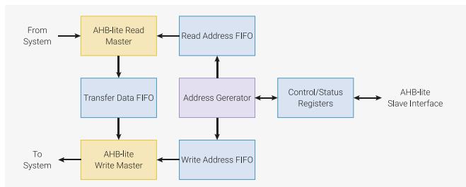
The DMA can perform one read access and one write access, up to 32 bits in size, every clock cycle. There are 12 independent channels, each which supervise a sequence of bus transfers, usually in one of the following scenarios:
- • Memory-to-peripheral: a peripheral signals the DMA when it needs more data to transmit. The DMA reads data from an array in RAM or flash, and writes to the peripheral's data FIFO.
- • Peripheral-to-memory: a peripheral signals the DMA when it has received data. The DMA reads this data from the peripheral's data FIFO, and writes it to an array in RAM.
- • Memory-to-memory: the DMA transfers data between two buffers in RAM, as fast as possible.
Each channel has its own control and status registers (CSRs), with which software can program and monitor the channel's progress. When multiple channels are active at the same time, the DMA shares bandwidth evenly between the channels, with round-robin over all channels which are currently requesting data transfers.
The transfer size can be either 32, 16, or 8 bits. This is configured once per channel: source transfer size and destination transfer size are the same. The DMA performs standard byte lane replication on narrow writes, so byte data is available in all 4 bytes of the databus, and halfword data in both halfwords.
Channels can be combined in varied ways for more sophisticated behaviour and greater autonomy. For example, one channel can configure another, loading configuration data from a sequence of control blocks in memory, and the second can then call back to the first via the CHAIN_TO option, when it needs to be reconfigured.
Making the DMA more autonomous means that much less processor supervision is required: overall this allows the system to do more at once, or to dissipate less power.
2.5.1. Configuring Channels
Each channel has four control/status registers:
- • READ_ADDR is a pointer to the next address to be read from
- • WRITE_ADDR is a pointer to the next address to be written to
- • TRANS_COUNT shows the number of transfers remaining in the current transfer sequence, and is used to program the number of transfers in the next transfer sequence (see Section 2.5.1.2 ).
- • CTRL is used to configure all other aspects of the channel's behaviour, to enable/disable it, and to check for completion.
These are live registers: they update continuously as the channel progresses.
2.5.1.1. Read and Write Addresses
READ_ADDR
and
WRITE_ADDR
contain the address the channel will next read from, and write to, respectively. These registers update automatically after each read/write access. They increment by 1, 2 or 4 bytes at a time, depending on the transfer size configured in
CTRL
.
Software should generally program these registers with new start addresses each time a new transfer sequence starts. If
READ_ADDR
and
WRITE_ADDR
are not reprogrammed, the DMA will use the current values as start addresses for the next transfer. For example:
- • If the address does not increment (e.g. it is the address of a peripheral FIFO), and the next transfer sequence is to/from that same address, there is no need to write to the register again.
- • When transferring to/from a consecutive series of buffers in memory (e.g. scattering and gathering), an address register will already have incremented to the start of the next buffer at the completion of a transfer.
By not programming all four CSRs for each transfer sequence, software can use shorter interrupt handlers, and more compact control block formats when used with channel chaining (see register aliases in Section 2.5.2.1 , chaining in Section 2.5.2.2 ).
 CAUTION
READ_ADDR
and
WRITE_ADDR
must always be aligned to the current transfer size, as specified in
CTRL.DATA_SIZE
. It is up to software to ensure the initial values are correctly aligned.
2.5.1.2. Transfer Count
Reading from
TRANS_COUNT
yields the number of transfers remaining in the current transfer sequence. This value updates continuously as the channel progresses. Writing to
TRANS_COUNT
sets the length of the
next
transfer sequence. Up to
\(
2^{32}-1
\)
transfers can be performed in one sequence.
Each time the channel starts a new transfer sequence, the most recent value written to
TRANS_COUNT
is copied to the live transfer counter, which will then start to decrement again as the new transfer sequence makes progress. For debugging purposes, the last value written can be read from the
DBG_TCR
(
TRANS_COUNT
reload value) register.
If the channel is triggered multiple times without intervening writes to
TRANS_COUNT
, it performs the same number of transfers each time. For example, when chained to, one channel might load a fixed-size control block into another channel's CSRs.
TRANS_COUNT
would be programmed once by software, and then reload automatically every time.
Alternatively,
TRANS_COUNT
can be written with a new value before starting each transfer sequence. If
TRANS_COUNT
is the channel trigger (see
Section 2.5.2.1
), the channel will start immediately, and the value just written will be used,
not
the value currently in the reload register.
 NOTE
NOTE
The
TRANS_COUNT
is the number of
transfers
to be performed. The total number of bytes transferred is
TRANS_COUNT
times the size of each transfer in bytes, given by
CTRL.DATA_SIZE
.
2.5.1.3. Control/Status
The
CTRL
register has more, smaller fields than the other 3 registers, and full details of these are given in the
CTRL
register listings. Among other things,
CTRL
is used to:
- • Configure the size of this channel's data transfers, via
CTRL.DATA_SIZE. Reads and writes are the same size. - • Configure if and how
READ_ADDRandWRITE_ADDRincrement after each read or write, viaCTRL.INCR_WRITE,CTRL.INCR_READ,CTRL.RING_SEL,CTRL.RING_SIZE. Ring transfers are available, where one of the address pointers wraps at some power-of-2 boundary.
- • Select another channel (or none) to be triggered when this channel completes, via
CTRL.CHAIN_TO. - • Select a peripheral data request (DREQ) signal to pace this channel's transfers, via
CTRL.TREQ_SEL. - • See when the channel is idle, via
CTRL.BUSY. - • See if the channel has encountered a bus error, e.g. due to a faulty address being accessed, via
CTRL.AHB_ERROR,CTRL.READ_ERROR, orCTRL.WRITE_ERROR.
2.5.2. Starting Channels
There are three ways to start a channel:
- • Writing to a channel trigger register
- • A chain trigger from another channel which has just completed, and has its
CHAIN_TOfield configured - • The
MULTI_CHAN_TRIGGERregister, which can start multiple channels at once
Each of these covers different use cases. For example, trigger registers are simple and efficient when configuring and starting a channel in an interrupt service routine, and
CHAIN_TO
allows one channel to callback to another channel, which can then reconfigure the first channel.
NOTE
Triggering a channel which is already running has no effect.
2.5.2.1. Aliases and Triggers
Table 118. Control register aliases. Each channel has four control/status registers. Each register can be accessed at multiple different addresses. In each naturally-aligned group of four, all four registers appear, in different orders.
| Offset | +0x0 | +0x4 | +0x8 | +0xC (Trigger) |
|---|---|---|---|---|
| 0x00 (Alias 0) | READ_ADDR | WRITE_ADDR | TRANS_COUNT | CTRL_TRIG |
| 0x10 (Alias 1) | CTRL | READ_ADDR | WRITE_ADDR | TRANS_COUNT_TRIG |
| 0x20 (Alias 2) | CTRL | TRANS_COUNT | READ_ADDR | WRITE_ADDR_TRIG |
| 0x30 (Alias 3) | CTRL | WRITE_ADDR | TRANS_COUNT | READ_ADDR_TRIG |
The four CSRs are aliased multiple times in memory. Each alias — of which there are four — exposes the same four physical registers, but in a different order. The final register in each alias (at offset
+0xC
, highlighted) is a trigger register. Writing to the trigger register starts the channel.
Often, only alias 0 is used, and aliases 1-3 can be ignored. The channel is configured
and
started by writing
READ_ADDR
,
WRITE_ADDR
,
TRANS_COUNT
and finally
CTRL
. Since
CTRL
is the trigger register in alias 0, this starts the channel.
The other aliases allow more compact control block lists when using one channel to configure another, and more efficient reconfiguration and launch in interrupt handlers:
- • Each CSR is a trigger register in one of the aliases:
- ◦ When gathering fixed-size buffers into a peripheral, the DMA channel can be configured and launched by writing only
READ_ADDR_TRIG. - ◦ When scattering from a peripheral to fixed-size buffers, the channel can be configured and launched by writing only
WRITE_ADDR_TRIG.
- ◦ When gathering fixed-size buffers into a peripheral, the DMA channel can be configured and launched by writing only
- • Useful combinations of registers appear as naturally-aligned tuples which contain a trigger register. In conjunction with channel chaining and address wrapping, these implement compressed control block formats, e.g.:
- ◦
(WRITE_ADDR, TRANS_COUNT_TRIG)for peripheral scatter operations
- ◦
- ◦ ( TRANS_COUNT , READ_ADDR_TRIG ) for peripheral gather operations, or calculating CRCs on a list of buffers
- ◦ ( READ_ADDR , WRITE_ADDR_TRIG ) for manipulating fixed-size buffers in memory
Trigger registers do not start the channel if:
- • The channel is disabled via CTRL.EN . (If the trigger is CTRL , the just-written value of EN is used, not the value currently in the CTRL register.)
- • The channel is already running
- • The value 0 is written to the trigger register. (This is useful for ending control block chains. See null triggers, Section 2.5.2.3 )
2.5.2.2. Chaining
When a channel completes, it can name a different channel to immediately be triggered. This can be used as a callback for the second channel to reconfigure and restart the first.
This feature is configured through the CHAIN_TO field in the channel CTRL register. This 4-bit value selects a channel that will start when this one finishes. A channel can not chain to itself. Setting CHAIN_TO to a channel's own index means no chaining will take place.
Chain triggers behave the same as triggers from other sources, such as trigger registers. For example, they cause TRANS_COUNT to reload, and they are ignored if the targeted channel is already running.
One application for CHAIN_TO is for a channel to request reconfiguration by another channel, from a sequence of control blocks in memory. Channel A is configured to perform a wrapped transfer from memory to channel B's control registers (including a trigger register), and channel B is configured to chain back to channel A when it completes each transfer sequence. This is shown more explicitly in the DMA control blocks example ( Section 2.5.6.2 ).
Use of the register aliases ( Section 2.5.2.1 ) enables compact formats for DMA control blocks: as little as one word in some cases.
Another use of chaining is a "ping-pong" configuration, where two channels each trigger one another. The processor can respond to the channel completion interrupts, and reconfigure each channel after it completes; however, the chained channel, which has already been configured, starts immediately. In other words, channel configuration and channel operation are pipelined. Performance can improve dramatically where many short transfer sequences are required.
The Section 2.5.6 goes into more detail on the possibilities of chain triggers, in the real world.
2.5.2.3. Null Triggers and Chain Interrupts
As mentioned in Section 2.5.2.1 , writing all-zeroes to a trigger register does not start the channel. This is called a null trigger, and it has two purposes:
- • Cause a halt at the end of an array of control blocks, by appending an all-zeroes block
- • Reduce the number of interrupts generated when control blocks are used
By default, a channel will generate an interrupt each time it finishes a transfer sequence, unless that channel's IRQ is masked in INTE0 or INTE1 . The rate of interrupts can be excessive, particularly as processor attention is generally not required while a sequence of control blocks are in progress; however, processor attention is required at the end of a chain.
The channel CTRL register has a field called IRQ_QUIET . Its default value is 0. When this set to 1, channels generate an interrupt when they receive a null trigger, and at no other time. The interrupt is generated by the channel which receives the trigger.
2.5.3. Data Request (DREQ)
Peripherals produce or consume data at their own pace. If the DMA simply transferred data as fast as possible, loss or corruption of data would ensue. DREQs are a communication channel between peripherals and the DMA, which enables the DMA to pace transfers according to the needs of the peripheral.
The
CTRL.TREQ_SEL
(transfer request) field selects an external DREQ. It can also be used to select one of the internal pacing timers, or select no TREQ at all (the transfer proceeds as fast as possible), e.g. for memory-to-memory transfers.
2.5.3.1. System DREQ Table
There is a global assignment of DREQ numbers to peripheral DREQ channels.
Table 119. DREQs
| DREQ | DREQ Channel | DREQ | DREQ Channel | DREQ | DREQ Channel | DREQ | DREQ Channel |
|---|---|---|---|---|---|---|---|
| 0 | DREQ_PIO0_TX0 | 10 | DREQ_PIO1_TX2 | 20 | DREQ_UART0_TX | 30 | DREQ_PWM_WRAP6 |
| 1 | DREQ_PIO0_TX1 | 11 | DREQ_PIO1_TX3 | 21 | DREQ_UART0_RX | 31 | DREQ_PWM_WRAP7 |
| 2 | DREQ_PIO0_TX2 | 12 | DREQ_PIO1_RX0 | 22 | DREQ_UART1_TX | 32 | DREQ_I2C0_TX |
| 3 | DREQ_PIO0_TX3 | 13 | DREQ_PIO1_RX1 | 23 | DREQ_UART1_RX | 33 | DREQ_I2C0_RX |
| 4 | DREQ_PIO0_RX0 | 14 | DREQ_PIO1_RX2 | 24 | DREQ_PWM_WRAP0 | 34 | DREQ_I2C1_TX |
| 5 | DREQ_PIO0_RX1 | 15 | DREQ_PIO1_RX3 | 25 | DREQ_PWM_WRAP1 | 35 | DREQ_I2C1_RX |
| 6 | DREQ_PIO0_RX2 | 16 | DREQ_SPI0_TX | 26 | DREQ_PWM_WRAP2 | 36 | DREQ_ADC |
| 7 | DREQ_PIO0_RX3 | 17 | DREQ_SPI0_RX | 27 | DREQ_PWM_WRAP3 | 37 | DREQ_XIP_STREAM |
| 8 | DREQ_PIO1_TX0 | 18 | DREQ_SPI1_TX | 28 | DREQ_PWM_WRAP4 | 38 | DREQ_XIP_SSITX |
| 9 | DREQ_PIO1_TX1 | 19 | DREQ_SPI1_RX | 29 | DREQ_PWM_WRAP5 | 39 | DREQ_XIP_SSIRX |
2.5.3.2. Credit-based DREQ Scheme
The RP2040 DMA is designed for systems where:
- • The area and power cost of large peripheral data FIFOs is prohibitive
- • The bandwidth demands of individual peripherals may be high, e.g. >50% bus injection rate for short periods
- • Bus latency is low, but multiple masters may be competing for bus access
In addition, the DMA's transfer FIFOs and dual-master structure permit multiple accesses to the same peripheral to be in flight at once, to improve gross throughput. Choice of DREQ mechanism is therefore critical:
- • The traditional "turn on the tap" method can cause overflow if multiple writes are backed up in the TDF. Some systems solve this by overprovisioning peripheral FIFOs and setting the DREQ threshold below the full level, but this wastes precious area and power
- • The ARM-style single and burst handshake does not permit additional requests to be registered while the current request is being served. This limits performance when FIFOs are very shallow.
The RP2040 DMA uses a credit-based DREQ mechanism. For each peripheral, the DMA attempts to keep as many transfers in flight as the peripheral has capacity for. This enables full bus throughput (1 word per clock) through an 8-deep peripheral FIFO with no possibility of overflow or underflow, in the absence of fabric latency or contention.
For each channel, the DMA maintains a counter. Each 1-clock pulse on the
dreq
signal will increment this counter (saturating). When nonzero, the channel requests a transfer from the DMA's internal arbiter, and the counter is decremented when the transfer is issued to the address FIFOs. At this point the transfer is in flight, but has not yet necessarily completed.
Figure 13. DREQ counting
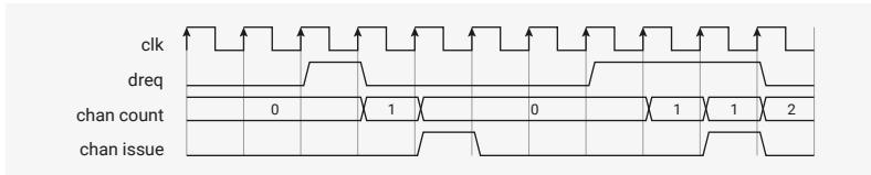
The diagram illustrates the DREQ counting mechanism. It shows four signals over time: clk (clock), dreq (data request), chan count (channel count), and chan issue (channel issue). The clk signal is a regular square wave. The dreq signal is a pulse that occurs at specific clock cycles. The chan count signal is a counter that increments from 0 to 2 as dreq pulses occur. The chan issue signal is a pulse that occurs at the end of each transfer sequence, corresponding to the chan count value.
The effect is to upper bound the number of in-flight transfers based on the amount of room or data available in the peripheral FIFO. In the steady state, this gives maximum throughput, but can't underflow or underflow.
One caveat is that the user must not access a FIFO which is currently being serviced by the DMA. This causes the channel and peripheral to become desynchronised, and can cause corruption or loss of data.
Another caveat is that multiple channels should not be connected to the same DREQ.
2.5.4. Interrupts
Each channel can generate interrupts; these can be masked on a per-channel basis using the INTE0 or INTE1 registers. There are two circumstances where a channel raises an interrupt request:
- • On the completion of each transfer sequence, if CTRL.IRQ_QUIET is disabled
- • On receiving a null trigger, if CTRL.IRQ_QUIET is enabled
The masked interrupt status is visible in the INTS registers; there is one bit for each channel. Interrupts are cleared by writing a bit mask to INTS . One idiom for acknowledging interrupts is to read INTS and then write the same value back, so only enabled interrupts are cleared.
The RP2040 DMA provides two system IRQs, with independent masking and status registers (e.g. INTE0 , INTE1 ). Any combination of channel interrupt requests can be routed to either system IRQ. For example:
- • Some channels can be given a higher priority in the system interrupt controller, if they have particularly tight timing requirements
- • In multiprocessor systems, different channel interrupts can be routed independently to different cores
For debugging purposes, the INTF registers can force either IRQ to be asserted.
2.5.5. Additional Features
2.5.5.1. Pacing Timers
These allow transfer of data roughly once every \( n \) clk_sys clocks instead of using external peripheral DREQ to trigger transfers. A fractional (X/Y) divider is used, and will generate a maximum of 1 request per clk_sys cycle.
There are 4 timers available in RP2040. Each DMA is able to select any of these in CTRL.TREQ_SEL .
2.5.5.2. CRC Calculation
The DMA can watch data from a given channel passing through the data FIFO, and calculate checksums based on this data. This is a purely passive affair: the data is not altered by this hardware, only observed.
The feature is controlled via the SNIFF_CTRL and SNIFF_DATA registers, and can be enabled/disabled per DMA transfer via the CTRL.SNIFF_EN field.
As this hardware cannot place backpressure on the FIFO, it must keep up with the DMA's maximum transfer rate of 32 bits per clock.
The supported checksums are:
- • CRC-32, MSB-first and LSB-first
- • CRC-16-CCITT, MSB-first and LSB-first
- • Simple summation (add to 32-bit accumulator)
- • Even parity
The result register is both readable and writable, so that the initial seed value can be set.
Bit/byte manipulations are available on the result which may aid specific use cases:
- • Bit inversion
- • Bit reversal
- • Byte swap
These manipulations do not affect the CRC calculation, just how the data is presented in the result register.
2.5.5.3. Channel Abort
It is possible for a channel to get into an irrecoverable state: e.g. if commanded to transfer more data than a peripheral will ever request, it will never complete. Clearing the
CTRL.EN
bit merely pauses the channel, and does not solve the problem. This should not occur under normal circumstances, but it is important that there is a mechanism to recover without simply hard-resetting the entire DMA block.
The
CHAN_ABORT
register forces channels to complete early. There is one bit for each channel, and writing a 1 terminates that channel. This clears the transfer counter and forces the channel into an inactive state.
 CAUTION
Due to RP2040-E13 , aborting a DMA channel that is making progress (i.e. not stalled on an inactive DREQ) may cause a completion IRQ to assert. The channel interrupt enable should be cleared before performing the abort, and the interrupt should be checked and cleared after the abort.
At the time an abort is triggered, a channel may have bus transfers currently in flight between the read and write master, and these transfers cannot be revoked. The
CTRL.BUSY
flag stays high until these transfers complete, and the channel reaches a safe state, which generally takes only a few cycles. The channel must not be restarted until its
CTRL.BUSY
flag deasserts. Starting a new sequence of transfers whilst transfers from an old sequence are still in flight can lead to unpredictable behaviour.
2.5.5.4. Debug
Debug registers are available for each DMA channel to show the dreq counter
DBG_CTDREQ
and next transfer count
DBG_TCR
. These can also be used to reset a DMA channel if required.
2.5.6. Example Use Cases
2.5.6.1. Using Interrupts to Reconfigure a Channel
When a channel finishes a block of transfers, it becomes available for making more transfers. Software detects that the channel is no longer busy, and reconfigures and restarts the channel. One approach is to poll the
CTRL.BUSY
bit until the channel is done, but this loses one of the key advantages of the DMA, namely that it does
not
have to operate in lockstep with a processor. By setting the correct bit in
INTE0
or
INTE1
, we can instruct the DMA to raise one of its two interrupt request lines when a given channel completes. Rather than repeatedly asking if a channel is done, we are told.
Having two system interrupt lines allows different channel completion interrupts to be routed to different cores, or to preempt one another on the same core if one channel is more time-critical.
When the interrupt is asserted, the processor can be configured to drop whatever it is doing and call a user-specified handler function. The handler can reconfigure and restart the channel. When the handler exits, the processor returns to the interrupted code running in the foreground.
Pico Examples: https://github.com/raspberrypi/pico-examples/blob/master/dma/channel_irq/channel_irq.c Lines 35 - 52
35 void dma_handler() {
36     static int pwm_level = 0;
37     static uint32_t wavetable[N_PWM_LEVELS];
38     static bool first_run = true;
39     // Entry number 'i' has 'i' one bits and '(32 - i)' zero bits.
40     if (first_run) {
41         first_run = false;
42         for (int i = 0; i < N_PWM_LEVELS; ++i)
43             wavetable[i] = ~(~0u << i);
44     }
45
46     // Clear the interrupt request.
47     dma_hw->ints0 = 1u << dma_chan;
48     // Give the channel a new wave table entry to read from, and re-trigger it
49     dma_channel_set_read_addr(dma_chan, &wavetable[pwm_level], true);
50
51     pwm_level = (pwm_level + 1) % N_PWM_LEVELS;
52 }
In many cases, most of the configuration can be done the first time the channel is started, and only addresses and transfer lengths need reprogramming in the DMA handler.
Pico Examples: https://github.com/raspberrypi/pico-examples/blob/master/dma/channel_irq/channel_irq.c Lines 54 - 94
54 int main() {
55     #ifndef PICO_DEFAULT_LED_PIN
56     //warning dma/channel_irq example requires a board with a regular LED
57     #else
58         // Set up a PIO state machine to serialise our bits
59         uint offset = pio_add_program(pio0, &pio_serialiser_program);
60         pio_serialiser_program_init(pio0, 0, offset, PICO_DEFAULT_LED_PIN, PIO_SERIAL_CLKDIV);
61
62         // Configure a channel to write the same word (32 bits) repeatedly to PIO0
63         // SM0's TX FIFO, paced by the data request signal from that peripheral.
64         dma_chan = dma_claim_unused_channel(true);
65         dma_channel_config c = dma_channel_get_default_config(dma_chan);
66         channel_config_set_transfer_data_size(&c, DMA_SIZE_32);
67         channel_config_set_read_increment(&c, false);
68         channel_config_set_dreq(&c, DREQ_PIO0_TX0);
69
70         dma_channel_configure(
71             dma_chan,
72             &c,
73             &pio0_hw->txf[0], // Write address (only need to set this once)
74             NULL,             // Don't provide a read address yet
75             PWM_REPEAT_COUNT, // Write the same value many times, then halt and interrupt
76             false             // Don't start yet
77         );
78 }
79 // Tell the DMA to raise IRQ line 0 when the channel finishes a block
80 dma_channel_set_irq0_enabled(dma_chan, true);
81
82 // Configure the processor to run dma_handler() when DMA IRQ 0 is asserted
83 irq_set_exclusive_handler(DMA_IRQ_0, dma_handler);
84 irq_set_enabled(DMA_IRQ_0, true);
85
86 // Manually call the handler once, to trigger the first transfer
87 dma_handler();
88
89 // Everything else from this point is interrupt-driven. The processor has
90 // time to sit and think about its early retirement -- maybe open a bakery?
91 while (true)
92     tight_loop_contents();
93 #endif
94 }
One disadvantage of this technique is that we don't start to reconfigure the channel until some time after the channel makes its last transfer. If there is heavy interrupt activity on the processor, this may be quite a long time, and therefore quite a large gap in transfers, which is problematic if we need to sustain a high data throughput.
This is solved by using two channels, with their
CHAIN_TO
fields crossed over, so that channel A triggers channel B when it completes, and vice versa. At any point in time, one of the channels is transferring data, and the other is either already configured to start the next transfer immediately when the current one finishes, or it is in the process of being reconfigured. When channel A completes, it immediately starts the cued-up transfer on channel B. At the same time, the interrupt is fired, and the handler reconfigures channel A so that it is ready for when channel B completes.
2.5.6.2. DMA Control Blocks
Frequently, multiple smaller buffers must be gathered together and sent to the same peripheral. To address this use case, the RP2040 DMA can execute a long and complex sequence of transfers without processor control. One channel repeatedly reconfigures a second channel, and the second channel restarts the first each time it completes block of transfers.
Because the first DMA channel is transferring data directly from memory to the second channel's control registers, the format of the control blocks in memory must match those registers. The last register written to, each time, will be one of the trigger registers (Section 2.5.2.1) which will start the second channel on its programmed block of transfers. The register aliases (Section 2.5.2.1) give some flexibility for the block layout, and more importantly allow some registers to be omitted from the blocks, so they occupy less memory and can be loaded more quickly.
This example shows how multiple buffers can be gathered and transferred to the UART, by reprogramming
TRANS_COUNT
and
READ_ADDR_TRIG
:
Pico Examples: https://github.com/raspberrypi/pico-examples/blob/master/dma/control_blocks/control_blocks.c
1 /**
2  * Copyright (c) 2020 Raspberry Pi (Trading) Ltd.
3  *
4  * SPDX-License-Identifier: BSD-3-Clause
5  */
6
7 // Use two DMA channels to make a programmed sequence of data transfers to the
8 // UART (a data gather operation). One channel is responsible for transferring
9 // the actual data, the other repeatedly reprograms that channel.
10
11 #include <stdio.h>
12 #include "pico/stdlib.h"
13 #include "hardware/dma.h"
14 #include "hardware/structs/uart.h"
15
16 // These buffers will be DMA'd to the UART, one after the other.
17
18 const char word0[] = "Transferring ";
19 const char word1[] = "one ";
20 const char word2[] = "word ";
21 const char word3[] = "at ";
22 const char word4[] = "a ";
23 const char word5[] = "time.\n";
24
25 // Note the order of the fields here: it's important that the length is before
26 // the read address, because the control channel is going to write to the last
27 // two registers in alias 3 on the data channel:
28 //           +0x0      +0x4      +0x8      +0xC (Trigger)
29 // Alias 0:  READ_ADDR  WRITE_ADDR  TRANS_COUNT  CTRL
30 // Alias 1:  CTRL      READ_ADDR  WRITE_ADDR  TRANS_COUNT
31 // Alias 2:  CTRL      TRANS_COUNT  READ_ADDR  WRITE_ADDR
32 // Alias 3:  CTRL      WRITE_ADDR  TRANS_COUNT  READ_ADDR
33 //
34 // This will program the transfer count and read address of the data channel,
35 // and trigger it. Once the data channel completes, it will restart the
36 // control channel (via CHAIN_T0) to load the next two words into its control
37 // registers.
38
39 const struct {uint32_t len; const char *data;} control_blocks[] = {
40     {count_of(word0) - 1, word0}, // Skip null terminator
41     {count_of(word1) - 1, word1},
42     {count_of(word2) - 1, word2},
43     {count_of(word3) - 1, word3},
44     {count_of(word4) - 1, word4},
45     {count_of(word5) - 1, word5},
46     {0, NULL} // Null trigger to end chain.
47 };
48
49 int main() {
50     #ifndef uart_default
51     //warning dma/control_blocks example requires a UART
52     #else
53         stdio_init_all();
54         puts("DMA control block example:");
55
56         // ctrl_chan loads control blocks into data_chan, which executes them.
57         int ctrl_chan = dma_claim_unused_channel(true);
58         int data_chan = dma_claim_unused_channel(true);
59
60         // The control channel transfers two words into the data channel's control
61         // registers, then halts. The write address wraps on a two-word
62         // (eight-byte) boundary, so that the control channel writes the same two
63         // registers when it is next triggered.
64
65         dma_channel_config c = dma_channel_get_default_config(ctrl_chan);
66         channel_config_set_transfer_data_size(&c, DMA_SIZE_32);
67         channel_config_set_read_increment(&c, true);
68         channel_config_set_write_increment(&c, true);
69         channel_config_set_ring(&c, true, 3); // 1 << 3 byte boundary on write ptr
70
71         dma_channel_configure(
72             ctrl_chan,
73             &c,
74             &dma_hw->ch[data_chan].a13_transfer_count, // Initial write address
75             &control_blocks[0], // Initial read address
76             2, // Halt after each control block
77             false // Don't start yet
78         );
79
80 // The data channel is set up to write to the UART FIFO (paced by the
81 // UART's TX data request signal) and then chain to the control channel
82 // once it completes. The control channel programs a new read address and
83 // data length, and retriggers the data channel.
84
85 c = dma_channel_get_default_config(data_chan);
86 channel_config_set_transfer_data_size(&c, DMA_SIZE_8);
87 channel_config_set_dreq(&c, uart_get_dreq(uart_default, true));
88 // Trigger ctrl_chan when data_chan completes
89 channel_config_set_chain_to(&c, ctrl_chan);
90 // Raise the IRQ flag when 0 is written to a trigger register (end of chain):
91 channel_config_set_irq_quiet(&c, true);
92
93 dma_channel_configure(
94     data_chan,
95     &c,
96     &uart_get_hw(uart_default)->dr,
97     NULL,          // Initial read address and transfer count are unimportant;
98     0,             // the control channel will reprogram them each time.
99     false          // Don't start yet.
100 );
101
102 // Everything is ready to go. Tell the control channel to load the first
103 // control block. Everything is automatic from here.
104 dma_start_channel_mask(1u << ctrl_chan);
105
106 // The data channel will assert its IRQ flag when it gets a null trigger,
107 // indicating the end of the control block list. We're just going to wait
108 // for the IRQ flag instead of setting up an interrupt handler.
109 while (!(dma_hw->intr & 1u << data_chan))
110     tight_loop_contents();
111 dma_hw->ints0 = 1u << data_chan;
112
113 puts("DMA finished.");
114 #endif
115 }
2.5.7. List of Registers
The DMA registers start at a base address of
0x50000000
(defined as
DMA_BASE
in SDK).
Table 120. List of DMA registers
| Offset | Name | Info |
|---|---|---|
| 0x000 | CH0_READ_ADDR | DMA Channel 0 Read Address pointer |
| 0x004 | CH0_WRITE_ADDR | DMA Channel 0 Write Address pointer |
| 0x008 | CH0_TRANS_COUNT | DMA Channel 0 Transfer Count |
| 0x00c | CH0_CTRL_TRIG | DMA Channel 0 Control and Status |
| 0x010 | CH0_AL1_CTRL | Alias for channel 0 CTRL register |
| 0x014 | CH0_AL1_READ_ADDR | Alias for channel 0 READ_ADDR register |
| 0x018 | CH0_AL1_WRITE_ADDR | Alias for channel 0 WRITE_ADDR register |
| 0x01c | CH0_AL1_TRANS_COUNT_TRIG | Alias for channel 0 TRANS_COUNT register This is a trigger register (0xc). Writing a nonzero value will reload the channel counter and start the channel. |
| 0x020 | CH0_AL2_CTRL | Alias for channel 0 CTRL register |
| Offset | Name | Info |
|---|---|---|
| 0x024 | CH0_AL2_TRANS_COUNT | Alias for channel 0 TRANS_COUNT register |
| 0x028 | CH0_AL2_READ_ADDR | Alias for channel 0 READ_ADDR register |
| 0x02c | CH0_AL2_WRITE_ADDR_TRIG | Alias for channel 0 WRITE_ADDR register This is a trigger register (0xc). Writing a nonzero value will reload the channel counter and start the channel. |
| 0x030 | CH0_AL3_CTRL | Alias for channel 0 CTRL register |
| 0x034 | CH0_AL3_WRITE_ADDR | Alias for channel 0 WRITE_ADDR register |
| 0x038 | CH0_AL3_TRANS_COUNT | Alias for channel 0 TRANS_COUNT register |
| 0x03c | CH0_AL3_READ_ADDR_TRIG | Alias for channel 0 READ_ADDR register This is a trigger register (0xc). Writing a nonzero value will reload the channel counter and start the channel. |
| 0x040 | CH1_READ_ADDR | DMA Channel 1 Read Address pointer |
| 0x044 | CH1_WRITE_ADDR | DMA Channel 1 Write Address pointer |
| 0x048 | CH1_TRANS_COUNT | DMA Channel 1 Transfer Count |
| 0x04c | CH1_CTRL_TRIG | DMA Channel 1 Control and Status |
| 0x050 | CH1_AL1_CTRL | Alias for channel 1 CTRL register |
| 0x054 | CH1_AL1_READ_ADDR | Alias for channel 1 READ_ADDR register |
| 0x058 | CH1_AL1_WRITE_ADDR | Alias for channel 1 WRITE_ADDR register |
| 0x05c | CH1_AL1_TRANS_COUNT_TRIG | Alias for channel 1 TRANS_COUNT register This is a trigger register (0xc). Writing a nonzero value will reload the channel counter and start the channel. |
| 0x060 | CH1_AL2_CTRL | Alias for channel 1 CTRL register |
| 0x064 | CH1_AL2_TRANS_COUNT | Alias for channel 1 TRANS_COUNT register |
| 0x068 | CH1_AL2_READ_ADDR | Alias for channel 1 READ_ADDR register |
| 0x06c | CH1_AL2_WRITE_ADDR_TRIG | Alias for channel 1 WRITE_ADDR register This is a trigger register (0xc). Writing a nonzero value will reload the channel counter and start the channel. |
| 0x070 | CH1_AL3_CTRL | Alias for channel 1 CTRL register |
| 0x074 | CH1_AL3_WRITE_ADDR | Alias for channel 1 WRITE_ADDR register |
| 0x078 | CH1_AL3_TRANS_COUNT | Alias for channel 1 TRANS_COUNT register |
| 0x07c | CH1_AL3_READ_ADDR_TRIG | Alias for channel 1 READ_ADDR register This is a trigger register (0xc). Writing a nonzero value will reload the channel counter and start the channel. |
| 0x080 | CH2_READ_ADDR | DMA Channel 2 Read Address pointer |
| 0x084 | CH2_WRITE_ADDR | DMA Channel 2 Write Address pointer |
| 0x088 | CH2_TRANS_COUNT | DMA Channel 2 Transfer Count |
| 0x08c | CH2_CTRL_TRIG | DMA Channel 2 Control and Status |
| 0x090 | CH2_AL1_CTRL | Alias for channel 2 CTRL register |
| 0x094 | CH2_AL1_READ_ADDR | Alias for channel 2 READ_ADDR register |
| Offset | Name | Info |
|---|---|---|
| 0x098 | CH2_AL1_WRITE_ADDR | Alias for channel 2 WRITE_ADDR register |
| 0x09c | CH2_AL1_TRANS_COUNT_TRIG | Alias for channel 2 TRANS_COUNT register This is a trigger register (0xc). Writing a nonzero value will reload the channel counter and start the channel. |
| 0x0a0 | CH2_AL2_CTRL | Alias for channel 2 CTRL register |
| 0x0a4 | CH2_AL2_TRANS_COUNT | Alias for channel 2 TRANS_COUNT register |
| 0x0a8 | CH2_AL2_READ_ADDR | Alias for channel 2 READ_ADDR register |
| 0x0ac | CH2_AL2_WRITE_ADDR_TRIG | Alias for channel 2 WRITE_ADDR register This is a trigger register (0xc). Writing a nonzero value will reload the channel counter and start the channel. |
| 0x0b0 | CH2_AL3_CTRL | Alias for channel 2 CTRL register |
| 0x0b4 | CH2_AL3_WRITE_ADDR | Alias for channel 2 WRITE_ADDR register |
| 0x0b8 | CH2_AL3_TRANS_COUNT | Alias for channel 2 TRANS_COUNT register |
| 0x0bc | CH2_AL3_READ_ADDR_TRIG | Alias for channel 2 READ_ADDR register This is a trigger register (0xc). Writing a nonzero value will reload the channel counter and start the channel. |
| 0x0c0 | CH3_READ_ADDR | DMA Channel 3 Read Address pointer |
| 0x0c4 | CH3_WRITE_ADDR | DMA Channel 3 Write Address pointer |
| 0x0c8 | CH3_TRANS_COUNT | DMA Channel 3 Transfer Count |
| 0x0cc | CH3_CTRL_TRIG | DMA Channel 3 Control and Status |
| 0x0d0 | CH3_AL1_CTRL | Alias for channel 3 CTRL register |
| 0x0d4 | CH3_AL1_READ_ADDR | Alias for channel 3 READ_ADDR register |
| 0x0d8 | CH3_AL1_WRITE_ADDR | Alias for channel 3 WRITE_ADDR register |
| 0x0dc | CH3_AL1_TRANS_COUNT_TRIG | Alias for channel 3 TRANS_COUNT register This is a trigger register (0xc). Writing a nonzero value will reload the channel counter and start the channel. |
| 0x0e0 | CH3_AL2_CTRL | Alias for channel 3 CTRL register |
| 0x0e4 | CH3_AL2_TRANS_COUNT | Alias for channel 3 TRANS_COUNT register |
| 0x0e8 | CH3_AL2_READ_ADDR | Alias for channel 3 READ_ADDR register |
| 0x0ec | CH3_AL2_WRITE_ADDR_TRIG | Alias for channel 3 WRITE_ADDR register This is a trigger register (0xc). Writing a nonzero value will reload the channel counter and start the channel. |
| 0x0f0 | CH3_AL3_CTRL | Alias for channel 3 CTRL register |
| 0x0f4 | CH3_AL3_WRITE_ADDR | Alias for channel 3 WRITE_ADDR register |
| 0x0f8 | CH3_AL3_TRANS_COUNT | Alias for channel 3 TRANS_COUNT register |
| 0x0fc | CH3_AL3_READ_ADDR_TRIG | Alias for channel 3 READ_ADDR register This is a trigger register (0xc). Writing a nonzero value will reload the channel counter and start the channel. |
| 0x100 | CH4_READ_ADDR | DMA Channel 4 Read Address pointer |
| 0x104 | CH4_WRITE_ADDR | DMA Channel 4 Write Address pointer |
| Offset | Name | Info |
|---|---|---|
| 0x108 | CH4_TRANS_COUNT | DMA Channel 4 Transfer Count |
| 0x10c | CH4_CTRL_TRIG | DMA Channel 4 Control and Status |
| 0x110 | CH4_AL1_CTRL | Alias for channel 4 CTRL register |
| 0x114 | CH4_AL1_READ_ADDR | Alias for channel 4 READ_ADDR register |
| 0x118 | CH4_AL1_WRITE_ADDR | Alias for channel 4 WRITE_ADDR register |
| 0x11c | CH4_AL1_TRANS_COUNT_TRIG | Alias for channel 4 TRANS_COUNT register This is a trigger register (0xc). Writing a nonzero value will reload the channel counter and start the channel. |
| 0x120 | CH4_AL2_CTRL | Alias for channel 4 CTRL register |
| 0x124 | CH4_AL2_TRANS_COUNT | Alias for channel 4 TRANS_COUNT register |
| 0x128 | CH4_AL2_READ_ADDR | Alias for channel 4 READ_ADDR register |
| 0x12c | CH4_AL2_WRITE_ADDR_TRIG | Alias for channel 4 WRITE_ADDR register This is a trigger register (0xc). Writing a nonzero value will reload the channel counter and start the channel. |
| 0x130 | CH4_AL3_CTRL | Alias for channel 4 CTRL register |
| 0x134 | CH4_AL3_WRITE_ADDR | Alias for channel 4 WRITE_ADDR register |
| 0x138 | CH4_AL3_TRANS_COUNT | Alias for channel 4 TRANS_COUNT register |
| 0x13c | CH4_AL3_READ_ADDR_TRIG | Alias for channel 4 READ_ADDR register This is a trigger register (0xc). Writing a nonzero value will reload the channel counter and start the channel. |
| 0x140 | CH5_READ_ADDR | DMA Channel 5 Read Address pointer |
| 0x144 | CH5_WRITE_ADDR | DMA Channel 5 Write Address pointer |
| 0x148 | CH5_TRANS_COUNT | DMA Channel 5 Transfer Count |
| 0x14c | CH5_CTRL_TRIG | DMA Channel 5 Control and Status |
| 0x150 | CH5_AL1_CTRL | Alias for channel 5 CTRL register |
| 0x154 | CH5_AL1_READ_ADDR | Alias for channel 5 READ_ADDR register |
| 0x158 | CH5_AL1_WRITE_ADDR | Alias for channel 5 WRITE_ADDR register |
| 0x15c | CH5_AL1_TRANS_COUNT_TRIG | Alias for channel 5 TRANS_COUNT register This is a trigger register (0xc). Writing a nonzero value will reload the channel counter and start the channel. |
| 0x160 | CH5_AL2_CTRL | Alias for channel 5 CTRL register |
| 0x164 | CH5_AL2_TRANS_COUNT | Alias for channel 5 TRANS_COUNT register |
| 0x168 | CH5_AL2_READ_ADDR | Alias for channel 5 READ_ADDR register |
| 0x16c | CH5_AL2_WRITE_ADDR_TRIG | Alias for channel 5 WRITE_ADDR register This is a trigger register (0xc). Writing a nonzero value will reload the channel counter and start the channel. |
| 0x170 | CH5_AL3_CTRL | Alias for channel 5 CTRL register |
| 0x174 | CH5_AL3_WRITE_ADDR | Alias for channel 5 WRITE_ADDR register |
| 0x178 | CH5_AL3_TRANS_COUNT | Alias for channel 5 TRANS_COUNT register |
| Offset | Name | Info |
|---|---|---|
| 0x17c | CH5_AL3_READ_ADDR_TRIG | Alias for channel 5 READ_ADDR register This is a trigger register (0xc). Writing a nonzero value will reload the channel counter and start the channel. |
| 0x180 | CH6_READ_ADDR | DMA Channel 6 Read Address pointer |
| 0x184 | CH6_WRITE_ADDR | DMA Channel 6 Write Address pointer |
| 0x188 | CH6_TRANS_COUNT | DMA Channel 6 Transfer Count |
| 0x18c | CH6_CTRL_TRIG | DMA Channel 6 Control and Status |
| 0x190 | CH6_AL1_CTRL | Alias for channel 6 CTRL register |
| 0x194 | CH6_AL1_READ_ADDR | Alias for channel 6 READ_ADDR register |
| 0x198 | CH6_AL1_WRITE_ADDR | Alias for channel 6 WRITE_ADDR register |
| 0x19c | CH6_AL1_TRANS_COUNT_TRIG | Alias for channel 6 TRANS_COUNT register This is a trigger register (0xc). Writing a nonzero value will reload the channel counter and start the channel. |
| 0x1a0 | CH6_AL2_CTRL | Alias for channel 6 CTRL register |
| 0x1a4 | CH6_AL2_TRANS_COUNT | Alias for channel 6 TRANS_COUNT register |
| 0x1a8 | CH6_AL2_READ_ADDR | Alias for channel 6 READ_ADDR register |
| 0x1ac | CH6_AL2_WRITE_ADDR_TRIG | Alias for channel 6 WRITE_ADDR register This is a trigger register (0xc). Writing a nonzero value will reload the channel counter and start the channel. |
| 0x1b0 | CH6_AL3_CTRL | Alias for channel 6 CTRL register |
| 0x1b4 | CH6_AL3_WRITE_ADDR | Alias for channel 6 WRITE_ADDR register |
| 0x1b8 | CH6_AL3_TRANS_COUNT | Alias for channel 6 TRANS_COUNT register |
| 0x1bc | CH6_AL3_READ_ADDR_TRIG | Alias for channel 6 READ_ADDR register This is a trigger register (0xc). Writing a nonzero value will reload the channel counter and start the channel. |
| 0x1c0 | CH7_READ_ADDR | DMA Channel 7 Read Address pointer |
| 0x1c4 | CH7_WRITE_ADDR | DMA Channel 7 Write Address pointer |
| 0x1c8 | CH7_TRANS_COUNT | DMA Channel 7 Transfer Count |
| 0x1cc | CH7_CTRL_TRIG | DMA Channel 7 Control and Status |
| 0x1d0 | CH7_AL1_CTRL | Alias for channel 7 CTRL register |
| 0x1d4 | CH7_AL1_READ_ADDR | Alias for channel 7 READ_ADDR register |
| 0x1d8 | CH7_AL1_WRITE_ADDR | Alias for channel 7 WRITE_ADDR register |
| 0x1dc | CH7_AL1_TRANS_COUNT_TRIG | Alias for channel 7 TRANS_COUNT register This is a trigger register (0xc). Writing a nonzero value will reload the channel counter and start the channel. |
| 0x1e0 | CH7_AL2_CTRL | Alias for channel 7 CTRL register |
| 0x1e4 | CH7_AL2_TRANS_COUNT | Alias for channel 7 TRANS_COUNT register |
| 0x1e8 | CH7_AL2_READ_ADDR | Alias for channel 7 READ_ADDR register |
| Offset | Name | Info |
|---|---|---|
| 0x1ec | CH7_AL2_WRITE_ADDR_TRIG | Alias for channel 7 WRITE_ADDR register This is a trigger register (0xc). Writing a nonzero value will reload the channel counter and start the channel. |
| 0x1f0 | CH7_AL3_CTRL | Alias for channel 7 CTRL register |
| 0x1f4 | CH7_AL3_WRITE_ADDR | Alias for channel 7 WRITE_ADDR register |
| 0x1f8 | CH7_AL3_TRANS_COUNT | Alias for channel 7 TRANS_COUNT register |
| 0x1fc | CH7_AL3_READ_ADDR_TRIG | Alias for channel 7 READ_ADDR register This is a trigger register (0xc). Writing a nonzero value will reload the channel counter and start the channel. |
| 0x200 | CH8_READ_ADDR | DMA Channel 8 Read Address pointer |
| 0x204 | CH8_WRITE_ADDR | DMA Channel 8 Write Address pointer |
| 0x208 | CH8_TRANS_COUNT | DMA Channel 8 Transfer Count |
| 0x20c | CH8_CTRL_TRIG | DMA Channel 8 Control and Status |
| 0x210 | CH8_AL1_CTRL | Alias for channel 8 CTRL register |
| 0x214 | CH8_AL1_READ_ADDR | Alias for channel 8 READ_ADDR register |
| 0x218 | CH8_AL1_WRITE_ADDR | Alias for channel 8 WRITE_ADDR register |
| 0x21c | CH8_AL1_TRANS_COUNT_TRIG | Alias for channel 8 TRANS_COUNT register This is a trigger register (0xc). Writing a nonzero value will reload the channel counter and start the channel. |
| 0x220 | CH8_AL2_CTRL | Alias for channel 8 CTRL register |
| 0x224 | CH8_AL2_TRANS_COUNT | Alias for channel 8 TRANS_COUNT register |
| 0x228 | CH8_AL2_READ_ADDR | Alias for channel 8 READ_ADDR register |
| 0x22c | CH8_AL2_WRITE_ADDR_TRIG | Alias for channel 8 WRITE_ADDR register This is a trigger register (0xc). Writing a nonzero value will reload the channel counter and start the channel. |
| 0x230 | CH8_AL3_CTRL | Alias for channel 8 CTRL register |
| 0x234 | CH8_AL3_WRITE_ADDR | Alias for channel 8 WRITE_ADDR register |
| 0x238 | CH8_AL3_TRANS_COUNT | Alias for channel 8 TRANS_COUNT register |
| 0x23c | CH8_AL3_READ_ADDR_TRIG | Alias for channel 8 READ_ADDR register This is a trigger register (0xc). Writing a nonzero value will reload the channel counter and start the channel. |
| 0x240 | CH9_READ_ADDR | DMA Channel 9 Read Address pointer |
| 0x244 | CH9_WRITE_ADDR | DMA Channel 9 Write Address pointer |
| 0x248 | CH9_TRANS_COUNT | DMA Channel 9 Transfer Count |
| 0x24c | CH9_CTRL_TRIG | DMA Channel 9 Control and Status |
| 0x250 | CH9_AL1_CTRL | Alias for channel 9 CTRL register |
| 0x254 | CH9_AL1_READ_ADDR | Alias for channel 9 READ_ADDR register |
| 0x258 | CH9_AL1_WRITE_ADDR | Alias for channel 9 WRITE_ADDR register |
| Offset | Name | Info |
|---|---|---|
| 0x25c | CH9_AL1_TRANS_COUNT_TRIG | Alias for channel 9 TRANS_COUNT register This is a trigger register (0xc). Writing a nonzero value will reload the channel counter and start the channel. |
| 0x260 | CH9_AL2_CTRL | Alias for channel 9 CTRL register |
| 0x264 | CH9_AL2_TRANS_COUNT | Alias for channel 9 TRANS_COUNT register |
| 0x268 | CH9_AL2_READ_ADDR | Alias for channel 9 READ_ADDR register |
| 0x26c | CH9_AL2_WRITE_ADDR_TRIG | Alias for channel 9 WRITE_ADDR register This is a trigger register (0xc). Writing a nonzero value will reload the channel counter and start the channel. |
| 0x270 | CH9_AL3_CTRL | Alias for channel 9 CTRL register |
| 0x274 | CH9_AL3_WRITE_ADDR | Alias for channel 9 WRITE_ADDR register |
| 0x278 | CH9_AL3_TRANS_COUNT | Alias for channel 9 TRANS_COUNT register |
| 0x27c | CH9_AL3_READ_ADDR_TRIG | Alias for channel 9 READ_ADDR register This is a trigger register (0xc). Writing a nonzero value will reload the channel counter and start the channel. |
| 0x280 | CH10_READ_ADDR | DMA Channel 10 Read Address pointer |
| 0x284 | CH10_WRITE_ADDR | DMA Channel 10 Write Address pointer |
| 0x288 | CH10_TRANS_COUNT | DMA Channel 10 Transfer Count |
| 0x28c | CH10_CTRL_TRIG | DMA Channel 10 Control and Status |
| 0x290 | CH10_AL1_CTRL | Alias for channel 10 CTRL register |
| 0x294 | CH10_AL1_READ_ADDR | Alias for channel 10 READ_ADDR register |
| 0x298 | CH10_AL1_WRITE_ADDR | Alias for channel 10 WRITE_ADDR register |
| 0x29c | CH10_AL1_TRANS_COUNT_TRIG | Alias for channel 10 TRANS_COUNT register This is a trigger register (0xc). Writing a nonzero value will reload the channel counter and start the channel. |
| 0x2a0 | CH10_AL2_CTRL | Alias for channel 10 CTRL register |
| 0x2a4 | CH10_AL2_TRANS_COUNT | Alias for channel 10 TRANS_COUNT register |
| 0x2a8 | CH10_AL2_READ_ADDR | Alias for channel 10 READ_ADDR register |
| 0x2ac | CH10_AL2_WRITE_ADDR_TRIG | Alias for channel 10 WRITE_ADDR register This is a trigger register (0xc). Writing a nonzero value will reload the channel counter and start the channel. |
| 0x2b0 | CH10_AL3_CTRL | Alias for channel 10 CTRL register |
| 0x2b4 | CH10_AL3_WRITE_ADDR | Alias for channel 10 WRITE_ADDR register |
| 0x2b8 | CH10_AL3_TRANS_COUNT | Alias for channel 10 TRANS_COUNT register |
| 0x2bc | CH10_AL3_READ_ADDR_TRIG | Alias for channel 10 READ_ADDR register This is a trigger register (0xc). Writing a nonzero value will reload the channel counter and start the channel. |
| 0x2c0 | CH11_READ_ADDR | DMA Channel 11 Read Address pointer |
| 0x2c4 | CH11_WRITE_ADDR | DMA Channel 11 Write Address pointer |
| 0x2c8 | CH11_TRANS_COUNT | DMA Channel 11 Transfer Count |
| Offset | Name | Info |
|---|---|---|
| 0x2cc | CH11_CTRL_TRIG | DMA Channel 11 Control and Status |
| 0x2d0 | CH11_AL1_CTRL | Alias for channel 11 CTRL register |
| 0x2d4 | CH11_AL1_READ_ADDR | Alias for channel 11 READ_ADDR register |
| 0x2d8 | CH11_AL1_WRITE_ADDR | Alias for channel 11 WRITE_ADDR register |
| 0x2dc | CH11_AL1_TRANS_COUNT_TRIG | Alias for channel 11 TRANS_COUNT register This is a trigger register (0xc). Writing a nonzero value will reload the channel counter and start the channel. |
| 0x2e0 | CH11_AL2_CTRL | Alias for channel 11 CTRL register |
| 0x2e4 | CH11_AL2_TRANS_COUNT | Alias for channel 11 TRANS_COUNT register |
| 0x2e8 | CH11_AL2_READ_ADDR | Alias for channel 11 READ_ADDR register |
| 0x2ec | CH11_AL2_WRITE_ADDR_TRIG | Alias for channel 11 WRITE_ADDR register This is a trigger register (0xc). Writing a nonzero value will reload the channel counter and start the channel. |
| 0x2f0 | CH11_AL3_CTRL | Alias for channel 11 CTRL register |
| 0x2f4 | CH11_AL3_WRITE_ADDR | Alias for channel 11 WRITE_ADDR register |
| 0x2f8 | CH11_AL3_TRANS_COUNT | Alias for channel 11 TRANS_COUNT register |
| 0x2fc | CH11_AL3_READ_ADDR_TRIG | Alias for channel 11 READ_ADDR register This is a trigger register (0xc). Writing a nonzero value will reload the channel counter and start the channel. |
| 0x400 | INTR | Interrupt Status (raw) |
| 0x404 | INTE0 | Interrupt Enables for IRQ 0 |
| 0x408 | INTF0 | Force Interrupts |
| 0x40c | INTS0 | Interrupt Status for IRQ 0 |
| 0x414 | INTE1 | Interrupt Enables for IRQ 1 |
| 0x418 | INTF1 | Force Interrupts for IRQ 1 |
| 0x41c | INTS1 | Interrupt Status (masked) for IRQ 1 |
| 0x420 | TIMER0 | Pacing (X/Y) Fractional Timer The pacing timer produces TREQ assertions at a rate set by \( ((X/Y) * \text{sys\_clk}) \) . This equation is evaluated every sys_clk cycles and therefore can only generate TREQs at a rate of 1 per sys_clk (i.e. permanent TREQ) or less. |
| 0x424 | TIMER1 | Pacing (X/Y) Fractional Timer The pacing timer produces TREQ assertions at a rate set by \( ((X/Y) * \text{sys\_clk}) \) . This equation is evaluated every sys_clk cycles and therefore can only generate TREQs at a rate of 1 per sys_clk (i.e. permanent TREQ) or less. |
| 0x428 | TIMER2 | Pacing (X/Y) Fractional Timer The pacing timer produces TREQ assertions at a rate set by \( ((X/Y) * \text{sys\_clk}) \) . This equation is evaluated every sys_clk cycles and therefore can only generate TREQs at a rate of 1 per sys_clk (i.e. permanent TREQ) or less. |
| Offset | Name | Info |
|---|---|---|
| 0x42c | TIMER3 | Pacing (X/Y) Fractional Timer The pacing timer produces TREQ assertions at a rate set by \( ((X/Y) * \text{sys\_clk}) \) . This equation is evaluated every sys_clk cycles and therefore can only generate TREQs at a rate of 1 per sys_clk (i.e. permanent TREQ) or less. |
| 0x430 | MULTI_CHAN_TRIGGER | Trigger one or more channels simultaneously |
| 0x434 | SNIFF_CTRL | Sniffer Control |
| 0x438 | SNIFF_DATA | Data accumulator for sniff hardware |
| 0x440 | FIFO_LEVELS | Debug RAF, WAF, TDF levels |
| 0x444 | CHAN_ABORT | Abort an in-progress transfer sequence on one or more channels |
| 0x448 | N_CHANNELS | The number of channels this DMA instance is equipped with. This DMA supports up to 16 hardware channels, but can be configured with as few as one, to minimise silicon area. |
| 0x800 | CH0_DBG_CTDREQ | Read: get channel DREQ counter (i.e. how many accesses the DMA expects it can perform on the peripheral without overflow/underflow. Write any value: clears the counter, and cause channel to re-initiate DREQ handshake. |
| 0x804 | CH0_DBG_TCR | Read to get channel TRANS_COUNT reload value, i.e. the length of the next transfer |
| 0x840 | CH1_DBG_CTDREQ | Read: get channel DREQ counter (i.e. how many accesses the DMA expects it can perform on the peripheral without overflow/underflow. Write any value: clears the counter, and cause channel to re-initiate DREQ handshake. |
| 0x844 | CH1_DBG_TCR | Read to get channel TRANS_COUNT reload value, i.e. the length of the next transfer |
| 0x880 | CH2_DBG_CTDREQ | Read: get channel DREQ counter (i.e. how many accesses the DMA expects it can perform on the peripheral without overflow/underflow. Write any value: clears the counter, and cause channel to re-initiate DREQ handshake. |
| 0x884 | CH2_DBG_TCR | Read to get channel TRANS_COUNT reload value, i.e. the length of the next transfer |
| 0x8c0 | CH3_DBG_CTDREQ | Read: get channel DREQ counter (i.e. how many accesses the DMA expects it can perform on the peripheral without overflow/underflow. Write any value: clears the counter, and cause channel to re-initiate DREQ handshake. |
| 0x8c4 | CH3_DBG_TCR | Read to get channel TRANS_COUNT reload value, i.e. the length of the next transfer |
| 0x900 | CH4_DBG_CTDREQ | Read: get channel DREQ counter (i.e. how many accesses the DMA expects it can perform on the peripheral without overflow/underflow. Write any value: clears the counter, and cause channel to re-initiate DREQ handshake. |
| 0x904 | CH4_DBG_TCR | Read to get channel TRANS_COUNT reload value, i.e. the length of the next transfer |
| Offset | Name | Info |
|---|---|---|
| 0x940 | CH5_DBG_CTDREQ | Read: get channel DREQ counter (i.e. how many accesses the DMA expects it can perform on the peripheral without overflow/underflow. Write any value: clears the counter, and cause channel to re-initiate DREQ handshake. |
| 0x944 | CH5_DBG_TCR | Read to get channel TRANS_COUNT reload value, i.e. the length of the next transfer |
| 0x980 | CH6_DBG_CTDREQ | Read: get channel DREQ counter (i.e. how many accesses the DMA expects it can perform on the peripheral without overflow/underflow. Write any value: clears the counter, and cause channel to re-initiate DREQ handshake. |
| 0x984 | CH6_DBG_TCR | Read to get channel TRANS_COUNT reload value, i.e. the length of the next transfer |
| 0x9c0 | CH7_DBG_CTDREQ | Read: get channel DREQ counter (i.e. how many accesses the DMA expects it can perform on the peripheral without overflow/underflow. Write any value: clears the counter, and cause channel to re-initiate DREQ handshake. |
| 0x9c4 | CH7_DBG_TCR | Read to get channel TRANS_COUNT reload value, i.e. the length of the next transfer |
| 0xa00 | CH8_DBG_CTDREQ | Read: get channel DREQ counter (i.e. how many accesses the DMA expects it can perform on the peripheral without overflow/underflow. Write any value: clears the counter, and cause channel to re-initiate DREQ handshake. |
| 0xa04 | CH8_DBG_TCR | Read to get channel TRANS_COUNT reload value, i.e. the length of the next transfer |
| 0xa40 | CH9_DBG_CTDREQ | Read: get channel DREQ counter (i.e. how many accesses the DMA expects it can perform on the peripheral without overflow/underflow. Write any value: clears the counter, and cause channel to re-initiate DREQ handshake. |
| 0xa44 | CH9_DBG_TCR | Read to get channel TRANS_COUNT reload value, i.e. the length of the next transfer |
| 0xa80 | CH10_DBG_CTDREQ | Read: get channel DREQ counter (i.e. how many accesses the DMA expects it can perform on the peripheral without overflow/underflow. Write any value: clears the counter, and cause channel to re-initiate DREQ handshake. |
| 0xa84 | CH10_DBG_TCR | Read to get channel TRANS_COUNT reload value, i.e. the length of the next transfer |
| 0xac0 | CH11_DBG_CTDREQ | Read: get channel DREQ counter (i.e. how many accesses the DMA expects it can perform on the peripheral without overflow/underflow. Write any value: clears the counter, and cause channel to re-initiate DREQ handshake. |
| 0xac4 | CH11_DBG_TCR | Read to get channel TRANS_COUNT reload value, i.e. the length of the next transfer |
DMA: CH0_READ_ADDR, CH1_READ_ADDR, ..., CH10_READ_ADDR, CH11_READ_ADDR Registers
Offsets: 0x000, 0x040, ..., 0x280, 0x2c0
Description DMA Channel N Read Address pointerTable 121.
CH0_READ_ADDR,
CH1_READ_ADDR, ...,
CH10_READ_ADDR,
CH11_READ_ADDR
Registers
| Bits | Description | Type | Reset |
|---|---|---|---|
| 31:0 | This register updates automatically each time a read completes. The current value is the next address to be read by this channel. | RW | 0x00000000 |
Table 122.
CH0_WRITE_ADDR,
CH1_WRITE_ADDR, ...,
CH10_WRITE_ADDR,
CH11_WRITE_ADDR
Registers
| Bits | Description | Type | Reset |
|---|---|---|---|
| 31:0 | This register updates automatically each time a write completes. The current value is the next address to be written by this channel. | RW | 0x00000000 |
Table 123.
CH0_TRANS_COUNT,
CH1_TRANS_COUNT,
...,
CH10_TRANS_COUNT,
CH11_TRANS_COUNT
Registers
| Bits | Description | Type | Reset |
|---|---|---|---|
| 31:0 | Program the number of bus transfers a channel will perform before halting. Note that, if transfers are larger than one byte in size, this is not equal to the number of bytes transferred (see CTRL_DATA_SIZE). When the channel is active, reading this register shows the number of transfers remaining, updating automatically each time a write transfer completes. Writing this register sets the RELOAD value for the transfer counter. Each time this channel is triggered, the RELOAD value is copied into the live transfer counter. The channel can be started multiple times, and will perform the same number of transfers each time, as programmed by most recent write. The RELOAD value can be observed at CHx_DBG_TCR. If TRANS_COUNT is used as a trigger, the written value is used immediately as the length of the new transfer sequence, as well as being written to RELOAD. | RW | 0x00000000 |
Table 124.
CH0_CTRL_TRIG,
CH1_CTRL_TRIG, ...,
CH10_CTRL_TRIG,
CH11_CTRL_TRIG
Registers
| Bits 14:10 9:5 4:0 Bits | Description SHIFT Description | MASK_MSB : The most-significant bit allowed to pass by the mask (inclusive) MASK_LSB : The least-significant bit allowed to pass by the mask (inclusive) : Logical right-shift applied to accumulator before masking | Type RW RW RW Type | Reset 0x00 0x00 0x00 Reset |
|---|---|---|---|---|
| 28:25 | Reserved. | - | - | |
| 24 | BUSY | : This flag goes high when the channel starts a new transfer sequence, BUSY is high pauses the channel, and BUSY will stay high while paused. | RO | 0x0 |
| 23 | SNIFF_EN | : If 1, this channel’s data transfers are visible to the sniff hardware, the sniff hardware is enabled, and has this channel selected. | RW | 0x0 |
| 22 | BSWAP | : Apply byte-swap transformation to DMA data. For byte data, this has no effect. For halfword data, the two bytes of each halfword are swapped. For word data, the four bytes of each word are swapped to reverse order. | RW | 0x0 |
| 21 | IRQ_QUIET | : In QUIET mode, the channel does not generate IRQs at the end of register, indicating the end of a control block chain. This reduces the number of interrupts to be serviced by the CPU when transferring a DMA chain of many small control blocks. | RW | 0x0 |
| 20:15 | TREQ_SEL | : Select a Transfer Request signal. The channel uses the transfer request signal to pace its data transfer rate. Sources for TREQ signals are internal (TIMERS) or external (DREQ, a Data Request from the system). | RW | 0x00 |
| 0x0 to 0x3a 0x3b → 0x3c → | → select DREQ n as TREQ Enumerated values: TIMER0: Select Timer 0 as TREQ TIMER1: Select Timer 1 as TREQ | |||
| 14:11 | 0x3f → 0x3e → 0x3d → CHAIN_TO | PERMANENT: Permanent request, for unpaced transfers. TIMER3: Select Timer 3 as TREQ (Optional) TIMER2: Select Timer 2 as TREQ (Optional) : When this channel completes, it will trigger the channel indicated | RW | 0x0 |
| by CHAIN_TO. Disable by setting CHAIN_TO = | (this channel) . | |||
| 10 | RING_SEL | : Select whether RING_SIZE applies to read or write addresses. addresses are wrapped. | RW | 0x0 |
| Bits | Description | Type | Reset |
|---|---|---|---|
| 9:6 | RING_SIZE: Size of address wrap region. If 0, don't wrap. For values \( n > 0 \) , only the lower \( n \) bits of the address will change. This wraps the address on a \( (1 \ll n) \) byte boundary, facilitating access to naturally-aligned ring buffers. Ring sizes between 2 and 32768 bytes are possible. This can apply to either read or write addresses, based on value of RING_SEL. | RW | 0x0 |
| Enumerated values: | |||
| 0x0 → RING_NONE | |||
| 5 | INCR_WRITE: If 1, the write address increments with each transfer. If 0, each write is directed to the same, initial address. Generally this should be disabled for memory-to-peripheral transfers. | RW | 0x0 |
| 4 | INCR_READ: If 1, the read address increments with each transfer. If 0, each read is directed to the same, initial address. Generally this should be disabled for peripheral-to-memory transfers. | RW | 0x0 |
| 3:2 | DATA_SIZE: Set the size of each bus transfer (byte/halfword/word). READ_ADDR and WRITE_ADDR advance by this amount (1/2/4 bytes) with each transfer. | RW | 0x0 |
| Enumerated values: | |||
| 0x0 → SIZE_BYTE | |||
| 0x1 → SIZE_HALFWORD | |||
| 0x2 → SIZE_WORD | |||
| 1 | HIGH_PRIORITY: HIGH_PRIORITY gives a channel preferential treatment in issue scheduling: in each scheduling round, all high priority channels are considered first, and then only a single low priority channel, before returning to the high priority channels. This only affects the order in which the DMA schedules channels. The DMA's bus priority is not changed. If the DMA is not saturated then a low priority channel will see no loss of throughput. | RW | 0x0 |
| 0 | EN: DMA Channel Enable. When 1, the channel will respond to triggering events, which will cause it to become BUSY and start transferring data. When 0, the channel will ignore triggers, stop issuing transfers, and pause the current transfer sequence (i.e. BUSY will remain high if already high) | RW | 0x0 |
DMA: CH0_AL1_CTRL, CH1_AL1_CTRL, ..., CH10_AL1_CTRL, CH11_AL1_CTRL Registers
Offsets: 0x010, 0x050, ..., 0x290, 0x2d0
Table 125.
CH0_AL1_CTRL,
CH1_AL1_CTRL, ...,
CH10_AL1_CTRL,
CH11_AL1_CTRL
Registers
| Bits | Description | Type | Reset |
|---|---|---|---|
| 31:0 | Alias for channel N CTRL register | RW | - |
DMA:
CH0_AL1_READ_ADDR, CH1_AL1_READ_ADDR, ...,
CH10_AL1_READ_ADDR, CH11_AL1_READ_ADDR Registers
Offsets: 0x014, 0x054, ..., 0x294, 0x2d4
Table 126.
CH0_AL1_READ_ADDR
,
CH1_AL1_READ_ADDR
, ...,
CH10_AL1_READ_ADDR,
CH11_AL1_READ_ADDR
Registers
| Bits | Description | Type | Reset |
|---|---|---|---|
| 31:0 | Alias for channel N READ_ADDR register | RW | - |
DMA:
CH0_AL1_WRITE_ADDR, CH1_AL1_WRITE_ADDR, ...,
CH10_AL1_WRITE_ADDR, CH11_AL1_WRITE_ADDR Registers
Offsets: 0x018, 0x058, ..., 0x298, 0x2d8
Table 127.
CH0_AL1_WRITE_ADDR,
CH1_AL1_WRITE_ADDR,
...,
CH10_AL1_WRITE_ADDR,
CH11_AL1_WRITE_ADDR
Registers
| Bits | Description | Type | Reset |
|---|---|---|---|
| 31:0 | Alias for channel N WRITE_ADDR register | RW | - |
DMA:
CH0_AL1_TRANS_COUNT_TRIG, CH1_AL1_TRANS_COUNT_TRIG, ...,
CH10_AL1_TRANS_COUNT_TRIG, CH11_AL1_TRANS_COUNT_TRIG Registers
Offsets: 0x01c, 0x05c, ..., 0x29c, 0x2dc
Table 128.
CH0_AL1_TRANS_COUNT_TRIG,
CH1_AL1_TRANS_COUNT_TRIG, ...,
CH10_AL1_TRANS_COUNT_TRIG,
CH11_AL1_TRANS_COUNT_TRIG
Registers
| Bits | Description | Type | Reset |
|---|---|---|---|
| 31:0 | Alias for channel N TRANS_COUNT register This is a trigger register (0xc). Writing a nonzero value will reload the channel counter and start the channel. | RW | - |
DMA:
CH0_AL2_CTRL, CH1_AL2_CTRL, ..., CH10_AL2_CTRL, CH11_AL2_CTRL
Registers
Offsets: 0x020, 0x060, ..., 0x2a0, 0x2e0
Table 129.
CH0_AL2_CTRL,
CH1_AL2_CTRL, ...,
CH10_AL2_CTRL,
CH11_AL2_CTRL
Registers
| Bits | Description | Type | Reset |
|---|---|---|---|
| 31:0 | Alias for channel N CTRL register | RW | - |
DMA:
CH0_AL2_TRANS_COUNT, CH1_AL2_TRANS_COUNT, ...,
CH10_AL2_TRANS_COUNT, CH11_AL2_TRANS_COUNT Registers
Offsets: 0x024, 0x064, ..., 0x2a4, 0x2e4
Table 130.
CH0_AL2_TRANS_COUNT,
CH1_AL2_TRANS_COUNT, ...,
CH10_AL2_TRANS_COUNT,
CH11_AL2_TRANS_COUNT
Registers
| Bits | Description | Type | Reset |
|---|---|---|---|
| 31:0 | Alias for channel N TRANS_COUNT register | RW | - |
DMA:
CH0_AL2_READ_ADDR, CH1_AL2_READ_ADDR, ...,
CH10_AL2_READ_ADDR, CH11_AL2_READ_ADDR Registers
Offsets: 0x028, 0x068, ..., 0x2a8, 0x2e8
Table 131.
CH0_AL2_READ_ADDR
,
CH1_AL2_READ_ADDR
, ...,
CH10_AL2_READ_ADDR
,
CH11_AL2_READ_ADDR
Registers
| Bits | Description | Type | Reset |
|---|---|---|---|
| 31:0 | Alias for channel N READ_ADDR register | RW | - |
DMA:
CH0_AL2_WRITE_ADDR_TRIG, CH1_AL2_WRITE_ADDR_TRIG, ...,
CH10_AL2_WRITE_ADDR_TRIG, CH11_AL2_WRITE_ADDR_TRIG Registers
Offsets: 0x02c, 0x06c, ..., 0x2ac, 0x2ec
Table 132.
CH0_AL2_WRITE_ADDR
_TRIG,
CH1_AL2_WRITE_ADDR
_TRIG, ...,
CH10_AL2_WRITE_ADDR
_TRIG,
CH11_AL2_WRITE_ADDR
_TRIG Registers
| Bits | Description | Type | Reset |
|---|---|---|---|
| 31:0 | Alias for channel N WRITE_ADDR register This is a trigger register (0xc). Writing a nonzero value will reload the channel counter and start the channel. | RW | - |
DMA:
CH0_AL3_CTRL, CH1_AL3_CTRL, ..., CH10_AL3_CTRL, CH11_AL3_CTRL
Registers
Offsets: 0x030, 0x070, ..., 0x2b0, 0x2f0
Table 133.
CH0_AL3_CTRL,
CH1_AL3_CTRL, ...,
CH10_AL3_CTRL,
CH11_AL3_CTRL
Registers
| Bits | Description | Type | Reset |
|---|---|---|---|
| 31:0 | Alias for channel N CTRL register | RW | - |
DMA:
CH0_AL3_WRITE_ADDR, CH1_AL3_WRITE_ADDR, ...,
CH10_AL3_WRITE_ADDR, CH11_AL3_WRITE_ADDR Registers
Offsets: 0x034, 0x074, ..., 0x2b4, 0x2f4
Table 134.
CH0_AL3_WRITE_ADDR
,
CH1_AL3_WRITE_ADDR
, ...,
CH10_AL3_WRITE_ADDR
,
CH11_AL3_WRITE_ADDR
Registers
| Bits | Description | Type | Reset |
|---|---|---|---|
| 31:0 | Alias for channel N WRITE_ADDR register | RW | - |
DMA:
CH0_AL3_TRANS_COUNT, CH1_AL3_TRANS_COUNT, ...,
CH10_AL3_TRANS_COUNT, CH11_AL3_TRANS_COUNT Registers
Offsets: 0x038, 0x078, ..., 0x2b8, 0x2f8
Table 135.
CH0_AL3_TRANS_COUNT,
CH1_AL3_TRANS_COUNT,
...,
CH10_AL3_TRANS_COUNT,
CH11_AL3_TRANS_COUNT
Registers
| Bits | Description | Type | Reset |
|---|---|---|---|
| 31:0 | Alias for channel N TRANS_COUNT register | RW | - |
DMA:
CH0_AL3_READ_ADDR_TRIG, CH1_AL3_READ_ADDR_TRIG, ...,
CH10_AL3_READ_ADDR_TRIG, CH11_AL3_READ_ADDR_TRIG Registers
Offsets: 0x03c, 0x07c, ..., 0x2bc, 0x2fc
Table 136.
CH0_AL3_READ_ADDR
_TRIG,
CH1_AL3_READ_ADDR
_TRIG, ...,
CH10_AL3_READ_ADDR
_TRIG,
CH11_AL3_READ_ADDR
_TRIG Registers
| Bits | Description | Type | Reset |
|---|---|---|---|
| 31:0 | Alias for channel N READ_ADDR register This is a trigger register (0xc). Writing a nonzero value will reload the channel counter and start the channel. | RW | - |
DMA: INTR Register
Offset: 0x400
Description
Interrupt Status (raw)
Table 137. INTR Register
| Bits | Description | Type | Reset |
|---|---|---|---|
| 31:16 | Reserved. | - | - |
| 15:0 | Raw interrupt status for DMA Channels 0..15. Bit n corresponds to channel n. Ignores any masking or forcing. Channel interrupts can be cleared by writing a bit mask to INTR, INTS0 or INTS1. Channel interrupts can be routed to either of two system-level IRQs based on INTE0 and INTE1. This can be used vector different channel interrupts to different ISRs: this might be done to allow NVIC IRQ preemption for more time-critical channels, or to spread IRQ load across different cores. It is also valid to ignore this behaviour and just use INTE0/INTS0/IRQ 0. | WC | 0x0000 |
DMA: INTE0 Register
Offset: 0x404
Description
Interrupt Enables for IRQ 0
Table 138. INTE0 Register
| Bits | Description | Type | Reset |
|---|---|---|---|
| 31:16 | Reserved. | - | - |
| 15:0 | Set bit n to pass interrupts from channel n to DMA IRQ 0. | RW | 0x0000 |
DMA: INTF0 Register
Offset: 0x408
Description
Force Interrupts
Table 139. INTF0 Register
| Bits | Description | Type | Reset |
|---|---|---|---|
| 31:16 | Reserved. | - | - |
| 15:0 | Write 1s to force the corresponding bits in INTE0. The interrupt remains asserted until INTF0 is cleared. | RW | 0x0000 |
DMA: INTS0 Register
Offset: 0x40c
Description
Interrupt Status for IRQ 0
Table 140. INTS0 Register
| Bits | Description | Type | Reset |
|---|---|---|---|
| 31:16 | Reserved. | - | - |
| 15:0 | Indicates active channel interrupt requests which are currently causing IRQ 0 to be asserted. Channel interrupts can be cleared by writing a bit mask here. | WC | 0x0000 |
DMA: INTE1 Register
Offset: 0x414
Description
Interrupt Enables for IRQ 1
Table 141. INTE1 Register
| Bits | Description | Type | Reset |
|---|---|---|---|
| 31:16 | Reserved. | - | - |
| 15:0 | Set bit n to pass interrupts from channel n to DMA IRQ 1. | RW | 0x0000 |
DMA: INTF1 Register
Offset: 0x418
Description
Force Interrupts for IRQ 1
Table 142. INTF1 Register
| Bits | Description | Type | Reset |
|---|---|---|---|
| 31:16 | Reserved. | - | - |
| 15:0 | Write 1s to force the corresponding bits in INTE0. The interrupt remains asserted until INTF0 is cleared. | RW | 0x0000 |
DMA: INTS1 Register
Offset: 0x41c
Description
Interrupt Status (masked) for IRQ 1
Table 143. INTS1 Register
| Bits | Description | Type | Reset |
|---|---|---|---|
| 31:16 | Reserved. | - | - |
| 15:0 | Indicates active channel interrupt requests which are currently causing IRQ 1 to be asserted. Channel interrupts can be cleared by writing a bit mask here. | WC | 0x0000 |
DMA: TIMER0, TIMER1, TIMER2, TIMER3 Registers
Offsets: 0x420, 0x424, 0x428, 0x42c
Description
Pacing (X/Y) Fractional Timer
The pacing timer produces TREQ assertions at a rate set by \( ((X/Y) * \text{sys\_clk}) \) . This equation is evaluated every \( \text{sys\_clk} \) cycles and therefore can only generate TREQs at a rate of 1 per \( \text{sys\_clk} \) (i.e. permanent TREQ) or less.
Table 144. TIMER0, TIMER1, TIMER2, TIMER3 Registers
| Bits | Description | Type | Reset |
|---|---|---|---|
| 31:16 | X: Pacing Timer Dividend. Specifies the X value for the (X/Y) fractional timer. | RW | 0x0000 |
| Bits | Description | Type | Reset |
|---|---|---|---|
| 15:0 | Y : Pacing Timer Divisor. Specifies the Y value for the (X/Y) fractional timer. | RW | 0x0000 |
DMA: MULTI_CHAN_TRIGGER Register
Offset: 0x430
Description
Trigger one or more channels simultaneously
Table 145.
MULTI_CHAN_TRIGGER Register
| Bits | Description | Type | Reset |
|---|---|---|---|
| 31:16 | Reserved. | - | - |
| 15:0 | Each bit in this register corresponds to a DMA channel. Writing a 1 to the relevant bit is the same as writing to that channel's trigger register; the channel will start if it is currently enabled and not already busy. | SC | 0x0000 |
DMA: SNIFF_CTRL Register
Offset: 0x434
Description
Sniffer Control
Table 146.
SNIFF_CTRL Register
| Bits | Description | Type | Reset |
|---|---|---|---|
| 31:12 | Reserved. | - | - |
| 11 | OUT_INV : If set, the result appears inverted (bitwise complement) when read. This does not affect the way the checksum is calculated; the result is transformed on-the-fly between the result register and the bus. | RW | 0x0 |
| 10 | OUT_REV : If set, the result appears bit-reversed when read. This does not affect the way the checksum is calculated; the result is transformed on-the-fly between the result register and the bus. | RW | 0x0 |
| 9 | BSWAP
: Locally perform a byte reverse on the sniffed data, before feeding into checksum. Note that the sniff hardware is downstream of the DMA channel byteswap performed in the read master: if channel CTRL_BSWAP and SNIFF_CTRL_BSWAP are both enabled, their effects cancel from the sniffer's point of view. | RW | 0x0 |
| 8:5 | CALC | RW | 0x0 |
| Enumerated values: | |||
| 0x0 → CRC32: Calculate a CRC-32 (IEEE802.3 polynomial) | |||
| 0x1 → CRC32R: Calculate a CRC-32 (IEEE802.3 polynomial) with bit reversed data | |||
| 0x2 → CRC16: Calculate a CRC-16-CCITT | |||
| 0x3 → CRC16R: Calculate a CRC-16-CCITT with bit reversed data | |||
| 0xe → EVEN: XOR reduction over all data. == 1 if the total 1 population count is odd. | |||
| 0xf → SUM: Calculate a simple 32-bit checksum (addition with a 32 bit accumulator) |
| Bits | Description | Type | Reset |
|---|---|---|---|
| 4:1 | DMACH : DMA channel for Sniffer to observe | RW | 0x0 |
| 0 | EN : Enable sniffer | RW | 0x0 |
DMA: SNIFF_DATA Register
Offset: 0x438
Description
Data accumulator for sniff hardware
Table 147.
SNIFF_DATA Register
| Bits | Description | Type | Reset |
|---|---|---|---|
| 31:0 | Write an initial seed value here before starting a DMA transfer on the channel indicated by SNIFF_CTRL_DMACH. The hardware will update this register each time it observes a read from the indicated channel. Once the channel completes, the final result can be read from this register. | RW | 0x00000000 |
DMA: FIFO_LEVELS Register
Offset: 0x440
Description
Debug RAF, WAF, TDF levels
Table 148.
FIFO_LEVELS Register
| Bits | Description | Type | Reset |
|---|---|---|---|
| 31:24 | Reserved. | - | - |
| 23:16 | RAF_LVL : Current Read-Address-FIFO fill level | RO | 0x00 |
| 15:8 | WAF_LVL : Current Write-Address-FIFO fill level | RO | 0x00 |
| 7:0 | TDF_LVL : Current Transfer-Data-FIFO fill level | RO | 0x00 |
DMA: CHAN_ABORT Register
Offset: 0x444
Description
Abort an in-progress transfer sequence on one or more channels
Table 149.
CHAN_ABORT
Register
| Bits | Description | Type | Reset |
|---|---|---|---|
| 31:16 | Reserved. | - | - |
| 15:0 | Each bit corresponds to a channel. Writing a 1 aborts whatever transfer sequence is in progress on that channel. The bit will remain high until any in-flight transfers have been flushed through the address and data FIFOs. After writing, this register must be polled until it returns all-zero. Until this point, it is unsafe to restart the channel. | SC | 0x0000 |
DMA: N_CHANNELS Register
Offset: 0x448
Table 150.
N_CHANNELS Register
| Bits | Description | Type | Reset |
|---|---|---|---|
| 31:5 | Reserved. | - | - |
| Bits | Description | Type | Reset |
|---|---|---|---|
| 4:0 | The number of channels this DMA instance is equipped with. This DMA supports up to 16 hardware channels, but can be configured with as few as one, to minimise silicon area. | RO | - |
DMA: CH0_DBG_CTDREQ, CH1_DBG_CTDREQ, ..., CH10_DBG_CTDREQ, CH11_DBG_CTDREQ Registers
Offsets: 0x800, 0x840, ..., 0xa80, 0xac0
Table 151.
CH0_DBG_CTDREQ,
CH1_DBG_CTDREQ, ...,
CH10_DBG_CTDREQ,
CH11_DBG_CTDREQ
Registers
| Bits | Description | Type | Reset |
|---|---|---|---|
| 31:6 | Reserved. | - | - |
| 5:0 | Read: get channel DREQ counter (i.e. how many accesses the DMA expects it can perform on the peripheral without overflow/underflow. Write any value: clears the counter, and cause channel to re-initiate DREQ handshake. | WC | 0x00 |
DMA: CH0_DBG_TCR, CH1_DBG_TCR, ..., CH10_DBG_TCR, CH11_DBG_TCR Registers
Offsets: 0x804, 0x844, ..., 0xa84, 0xac4
Table 152.
CH0_DBG_TCR,
CH1_DBG_TCR, ...,
CH10_DBG_TCR,
CH11_DBG_TCR
Registers
| Bits | Description | Type | Reset |
|---|---|---|---|
| 31:0 | Read to get channel TRANS_COUNT reload value, i.e. the length of the next transfer | RO | 0x00000000 |
2.6. Memory
RP2040 has embedded ROM and SRAM, and access to external Flash via a QSPI interface. Details of internal memory are given below.
2.6.1. ROM
A 16kB read-only memory (ROM) is at address
0x00000000
. The ROM contents are fixed at the time the silicon is manufactured. It contains:
- • Initial startup routine
- • Flash boot sequence
- • Flash programming routines
- • USB mass storage device with UF2 support
- • Utility libraries such as fast floating point
The boot sequence of the chip is defined in Section 2.8.1 , and the ROM contents is described in more detail in Section 2.8 . The full source code for the RP2040 bootrom is available at:
The ROM offers single-cycle read-only bus access, and is on a dedicated AHB-Lite arbiter, so it can be accessed simultaneously with other memory devices. Attempting to write to the ROM has no effect (no bus fault is generated).
2.6.2. SRAM
There is a total of 264kB of on-chip SRAM. Physically this is partitioned into six banks, as this vastly improves memory bandwidth for multiple masters, but software may treat it as a single 264kB memory region. There are no restrictions on what is stored in each bank: processor code, data buffers, or a mixture. There are four 16k x 32-bit banks (64kB each) and two 1k x 32-bit banks (4kB each).
! IMPORTANT
Banking is a physical partitioning of SRAM which improves performance by allowing multiple simultaneous accesses. Logically there is a single 264kB contiguous memory.
Each SRAM bank is accessed via a dedicated AHB-Lite arbiter. This means different bus masters can access different SRAM banks in parallel, so up to four 32-bit SRAM accesses can take place every system clock cycle (one per master).
SRAM is mapped to system addresses starting at
0x20000000
. The first 256kB address region is word-striped across the four larger banks, which provides a significant memory parallelism benefits for most use cases.
Consecutive words in the system address space are routed to different RAM banks as shown in Table 153 .
Table 153. SRAM bank0/1/2/3 striped mapping.
| System address | SRAM Bank | SRAM word address |
|---|---|---|
0x20000000 | Bank 0 | 0 |
0x20000004 | Bank 1 | 0 |
0x20000008 | Bank 2 | 0 |
0x2000000c | Bank 3 | 0 |
0x20000010 | Bank 0 | 1 |
0x20000014 | Bank 1 | 1 |
0x20000018 | Bank 2 | 1 |
0x2000001c | Bank 3 | 1 |
0x20000020 | Bank 0 | 2 |
0x20000024 | Bank 1 | 2 |
0x20000028 | Bank 2 | 2 |
0x2000002c | Bank 3 | 2 |
| etc |
The next two 4kB regions (starting at
0x20040000
and
0x20041000
) are mapped directly to the smaller, 4kB memory banks. Software
may
choose to use these for per-core purposes, e.g. stack and frequently-executed code, guaranteeing that the processors never stall on these accesses. However, like all SRAM on RP2040, these banks have single-cycle access from
all
masters providing no other masters are accessing the bank in the same cycle, so it is reasonable to treat memory as a single 264kB device.
The four 64kB banks are also available at a non-striped mirror. The four 64kB regions starting at
0x21000000
,
0x21010000
,
0x21020000
,
0x21030000
are each mapped directly to one of the four 64kB SRAM banks. Software can explicitly allocate data and code across the physical memory banks, for improved memory performance in exceptionally demanding cases. This is often unnecessary, as memory striping usually provides sufficient parallelism with less software complexity.
The non-striped mirror starts at an offset of +16MB above the base of SRAM, as this is the maximum offset that allows ARMv6M subroutine calls between the smaller banks and the non-striped larger banks.
2.6.2.1. Other On-chip Memory
Besides the 264kB main memory, there are two other dedicated RAM blocks that may be used in some circumstances:
- • If flash XIP caching is disabled, the cache becomes available as a 16kB memory starting at
0x15000000 - • If the USB is not used, the USB data DPRAM can be used as a 4kB memory starting at
0x50100000
This gives a total of 284kB of on-chip SRAM. There are no restrictions on how these memories are used, e.g. it is possible to execute code from the USB data RAM if you choose.
2.6.3. Flash
External Flash is accessed via the QSPI interface using the execute-in-place (XIP) hardware. This allows an external flash memory to be addressed and accessed by the system as though it were internal memory. Bus reads to a 16MB memory window starting at
0x10000000
are translated into a serial flash transfer, and the result is returned to the master that initiated the read. This process is transparent to the master, so a processor can execute code from the external flash without first copying the code to internal memory, hence "execute in place". An internal cache remembers the contents of recently-accessed flash locations, which accelerates the average bandwidth and latency of the interface.
Once correctly configured by RP2040's bootrom and the flash second stage, the XIP hardware is largely transparent, and software can treat flash as a large read-only memory. However, it does provide a number of additional features to serve more demanding software use cases.
Figure 14. Flash execute-in-place (XIP) subsystem. System accesses via the main AHB-Lite slave are decoded to determine if they are XIP accesses, direct accesses to the SSI e.g. for configuration, or accesses to various other hardware and control registers in the XIP subsystem. XIP accesses are first looked up in the cache, to accelerate accesses to recently-used data. If the data is not found in the cache, an external serial access is generated via the SSI, and the resulting data is stored in the cache and forwarded on to the system bus.
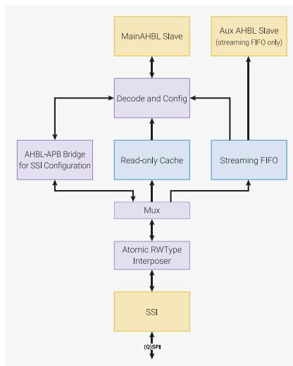
graph TD
    MainAHBL[MainAHBL Slave] <--> Decode[Decode and Config]
    Decode <--> AHBLBridge[AHBL-APB Bridge for SSI Configuration]
    Decode <--> Cache[Read-only Cache]
    Decode <--> StreamingFIFO[Streaming FIFO]
    Cache <--> Mux[Mux]
    Mux <--> Interposer[Atomic RWType Interposer]
    Interposer <--> SSI[SSI]
    SSI <--> QSPI[QSPI]
    StreamingFIFO <--> AuxAHBL[Aux AHBL Slave (streaming FIFO only)]
NOTE
The serial flash interface is configured by the flash second stage when using the SDK to run at an integer divider of the system clock. All the included second stage boot implementations support a
PICO_FLASH_SPI_CLKDIV
setting (e.g. defaulted to 4 in
https://github.com/raspberrypi/pico-sdk/blob/master/src/rp2040/boot_stage2/boot2_w25q080.S
to make the default interface speed
\(
125/4 = 31.25\text{MHz}
\)
). This divider can be overridden by specifying
PICO_FLASH_SPI_CLKDIV
in the particular board config header used with the SDK.
2.6.3.1. XIP Cache
The cache is 16kB, two way set-associative, 1 cycle hit. It is internal to the XIP subsystem, and only affects accesses to XIP flash, so software does not have to consider cache coherence, unless performing flash programming operations. It caches reads from a 24-bit flash address space, which is mirrored multiple times in the RP2040 address space, each alias having different caching behaviour. The eight MSBs of the system address are used for segment decode, leaving 24 bits for flash addressing, so the maximum supported flash size (for XIP operation) is 16MB. The available mirrors
are:
- • 0x10... XIP access, cacheable, allocating - Normal cache operation
- • 0x11... XIP access, cacheable, non-allocating - Check for hit, don't update cache on miss
- • 0x12... XIP access, non-cacheable, allocating - Don't check for hit, always update cache
- • 0x13... XIP access, non-cacheable, non-allocating - Bypass cache completely
- • 0x15... Use XIP cache as SRAM bank, mirrored across entire segment
If the cache is disabled, via the CTRL.EN register bit, then all four of the XIP aliases ( 0x10 to 0x13 ) will bypass the cache, and access the flash directly. This has a significant impact on XIP code execution performance.
Access to the 0x15... segment produces a bus error unless the cache is disabled by clearing CTRL.EN . Once the cache is disabled, this region behaves as an additional 16kB SRAM bank. Reads and writes are one cycle, but there is a wait state on consecutive write-read sequences, i.e. there is no write forwarding buffer.
2.6.3.2. Cache Flushing and Maintenance
The FLUSH register allows the entire cache contents to be flushed. This is necessary if software has reprogrammed the flash contents, and needs to clear out stale data and code, without performing a reboot. Cache flushes are triggered either manually by writing 1 to FLUSH , or automatically when the XIP block is brought out of reset. The flush is implemented by zeroing the cache tag memory using an internal counter, which takes just over 1024 clock cycles (16kB total size / 8 bytes per line / 2 ways per set).
Flushing the cache whilst accessing flash data (perhaps initiating the flush on one core whilst another core may be executing code from flash) is a safe operation, but any master accessing flash data while the flush is in progress will be stalled until completion.
 CAUTION
The cache-as-SRAM alias ( 0x15... ) must not be written whilst a cache flush is in progress. Before writing for the first time, if a cache flush has recently been initiated (e.g. via a watchdog reset), a dummy read from FLUSH is recommended to ensure the cache flush has completed. Writing to cache-as-SRAM whilst a flush is in progress can corrupt the data memory contents.
A complete cache flush dramatically slows subsequent code execution, until the cache "warms up" again. There is an alternative, which allows cache contents corresponding to only a certain address range to be invalidated. A write to the 0x10... mirror will look up the addressed location in the cache, and delete any matching entry found. Writing to all word-aligned locations in an address range (e.g. a flash sector that has just been erased and reprogrammed) therefore eliminates the possibility of stale cached data in this range, without suffering the effects of a complete cache flush.
Pico Examples: https://github.com/raspberrypi/pico-examples/blob/master/flash/cache_perfctr/flash_cache_perfctr.c Lines 30 - 55
30 // Flush cache to make sure we miss the first time we access test_data
31 xip_ctrl_hw->flush = 1;
32 while (!(xip_ctrl_hw->stat & XIP_STAT_FLUSH_READY_BITS))
33     tight_loop_contents();
34
35 // Clear counters (write any value to clear)
36 xip_ctrl_hw->ctr_acc = 1;
37 xip_ctrl_hw->ctr_hit = 1;
38
39 (void) *test_data_ptr;
40 check(xip_ctrl_hw->ctr_hit == 0 && xip_ctrl_hw->ctr_acc == 1,
41     "First access to data should miss");
42
43 (void) *test_data_ptr;
44 check(xip_ctrl_hw->ctr_hit == 1 && xip_ctrl_hw->ctr_acc == 2,
45     "Second access to data should hit");
46
47     // Write to invalidate individual cache lines (64 bits)
48     // Writes must be directed to the cacheable, allocatable alias (address 0x10.....)
49     *test_data_ptr = 0;
50     (void) *test_data_ptr;
51     check(xip_ctrl_hw->ctr_hit == 1 && xip_ctrl_hw->ctr_acc == 3,
52          "Should miss after invalidation");
53     (void) *test_data_ptr;
54     check(xip_ctrl_hw->ctr_hit == 2 && xip_ctrl_hw->ctr_acc == 4,
55          "Second access after invalidation should hit again");
2.6.3.3. SSI
The execute-in-place functionality is provided by the SSI interface, documented in Section 4.10 . It supports 1, 2 or 4-bit SPI flash interfaces (SPI, DSPI and QSPI), and can insert either an instruction prefix or mode continuation bits on each XIP access. This includes the possibility of issuing a standard 03h serial flash read command for each access, allowing virtually any serial flash device to be used. The maximum SPI clock frequency is half the system clock frequency.
The SSI can also be used as a standard FIFO-based SPI master, with DMA support. This mode is used by the bootrom to extract the second stage bootloader from external flash (see Section 2.8.1 ). The bus interposer allows an atomic set, clear or XOR operation to be posted to SSI control registers, in the same manner as other memory-mapped IO on RP2040. This is described in more detail in Section 2.1.2 .
2.6.3.4. Flash Streaming and Auxiliary Bus Slave
As the flash is generally much larger than SRAM, it's often useful to stream chunks of data into memory from flash. It's convenient to have the DMA stream this data in the background while software in the foreground is doing other things, and it's even more convenient if code can continue to execute from flash whilst this takes place.
This doesn't interact well with standard XIP operation, because of the lengthy bus stalls forced on the DMA whilst the SSI is performing serial transfers. These stalls are tolerable for a processor, because an in-order processor tends to have nothing better to do while waiting for an instruction fetch to retire, and because typical code execution tends to have much higher cache hit rates than bulk streaming of infrequently accessed data. In contrast, stalling the DMA prevents any other active DMA channels from making progress during this time, which slows overall DMA throughput.
The STREAM_ADDR and STREAM_CTR registers are used to program a linear sequence of flash reads, which the XIP subsystem will perform in the background in a best-effort fashion. To minimise impact on code being executed from flash whilst the stream is ongoing, the streaming hardware has lower priority access to the SSI than regular XIP accesses, and there is a brief cooldown (seven cycles) between the last XIP cache miss and resuming streaming. This helps to avoid increase in initial access latency on XIP cache miss.
Pico Examples: https://github.com/raspberrypi/pico-examples/blob/master/flash/xip_stream/flash_xip_stream.c Lines 45 - 48
45     while (!(xip_ctrl_hw->stat & XIP_STAT_FIFO_EMPTY))
46         (void) xip_ctrl_hw->stream_fifo;
47     xip_ctrl_hw->stream_addr = (uint32_t) &random_test_data[0];
48     xip_ctrl_hw->stream_ctr = count_of(random_test_data);
The streamed data is pushed to a small FIFO, which generates DREQ signals, telling the DMA to collect the streamed data. As the DMA does not initiate a read until after the data has been read from flash, the DMA is not stalled when accessing the data.
Although this scheme ensures that the data is ready in the streaming FIFO once the DREQ is asserted, the DMA can still be stalled if another master is currently stalled on the XIP slave, e.g. due to a cache miss. This is solved by the auxiliary bus slave, which is a simple bus interface providing access only to the streaming FIFO. This slave is exposed on the
FASTPERI arbiter, which services only native AHB-Lite peripherals which don't generate wait states, so the DMA will never experience stalls when accessing the FIFO at this address, assuming it has high bus priority.
Pico Examples: https://github.com/raspberrypi/pico-examples/blob/master/flash/xip_stream/flash_xip_stream.c Lines 58 - 70
58     const uint dma_chan = 0;
59     dma_channel_config cfg = dma_channel_get_default_config(dma_chan);
60     channel_config_set_read_increment(&cfg, false);
61     channel_config_set_write_increment(&cfg, true);
62     channel_config_set_dreq(&cfg, DREQ_XIP_STREAM);
63     dma_channel_configure(
64         dma_chan,
65         &cfg,
66         (void *) buf,           // Write addr
67         (const void *) XIP_AUX_BASE, // Read addr
68         count_of(random_test_data), // Transfer count
69         true                    // Start immediately!
70     );
2.6.3.5. Performance Counters
The XIP subsystem provides two performance counters. These are 32 bits in size, saturate upon reaching 0xffffffff, and are cleared by writing any value. They count:
- 1. The total number of XIP accesses, to any alias
- 2. The number of XIP accesses which resulted in a cache hit
For common use cases, this allows the cache hit rate to be profiled.
2.6.3.6. List of XIP Registers
The XIP registers start at a base address of 0x14000000 (defined as XIP_CTRL_BASE in SDK).
Table 154. List of XIP registers
| Offset | Name | Info |
|---|---|---|
| 0x00 | CTRL | Cache control |
| 0x04 | FLUSH | Cache Flush control |
| 0x08 | STAT | Cache Status |
| 0x0c | CTR_HIT | Cache Hit counter |
| 0x10 | CTR_ACC | Cache Access counter |
| 0x14 | STREAM_ADDR | FIFO stream address |
| 0x18 | STREAM_CTR | FIFO stream control |
| 0x1c | STREAM_FIFO | FIFO stream data |
XIP: CTRL Register
Offset: 0x00
Description
Cache control
Table 155. CTRL Register
| Bits | Description | Type | Reset |
|---|---|---|---|
| 31:4 | Reserved. | - | - |
| 3 | POWER_DOWN: When 1, the cache memories are powered down. They retain state, but can not be accessed. This reduces static power dissipation. Writing 1 to this bit forces CTRL_EN to 0, i.e. the cache cannot be enabled when powered down. Cache-as-SRAM accesses will produce a bus error response when the cache is powered down. | RW | 0x0 |
| 2 | Reserved. | - | - |
| 1 | ERR_BADWRITE: When 1, writes to any alias other than 0x0 (caching, allocating) will produce a bus fault. When 0, these writes are silently ignored. In either case, writes to the 0x0 alias will deallocate on tag match, as usual. | RW | 0x1 |
| 0 | EN:
When 1, enable the cache. When the cache is disabled, all XIP accesses will go straight to the flash, without querying the cache. When enabled, cacheable XIP accesses will query the cache, and the flash will not be accessed if the tag matches and the valid bit is set. If the cache is enabled, cache-as-SRAM accesses have no effect on the cache data RAM, and will produce a bus error response. | RW | 0x1 |
XIP: FLUSH Register
Offset: 0x04
Description
Cache Flush control
Table 156. FLUSH Register
| Bits | Description | Type | Reset |
|---|---|---|---|
| 31:1 | Reserved. | - | - |
| 0 | Write 1 to flush the cache. This clears the tag memory, but the data memory retains its contents. (This means cache-as-SRAM contents is not affected by flush or reset.) Reading will hold the bus (stall the processor) until the flush completes. Alternatively STAT can be polled until completion. | SC | 0x0 |
XIP: STAT Register
Offset: 0x08
Description
Cache Status
Table 157. STAT Register
| Bits | Description | Type | Reset |
|---|---|---|---|
| 31:3 | Reserved. | - | - |
| 2 | FIFO_FULL: When 1, indicates the XIP streaming FIFO is completely full. The streaming FIFO is 2 entries deep, so the full and empty flag allow its level to be ascertained. | RO | 0x0 |
| 1 | FIFO_EMPTY: When 1, indicates the XIP streaming FIFO is completely empty. | RO | 0x1 |
| Bits | Description | Type | Reset |
|---|---|---|---|
| 0 | FLUSH_READY:
Reads as 0 while a cache flush is in progress, and 1 otherwise. The cache is flushed whenever the XIP block is reset, and also when requested via the FLUSH register. | RO | 0x0 |
XIP: CTR_HIT Register
Offset: 0x0c
Description
Cache Hit counter
Table 158. CTR_HIT Register
| Bits | Description | Type | Reset |
|---|---|---|---|
| 31:0 | A 32 bit saturating counter that increments upon each cache hit, i.e. when an XIP access is serviced directly from cached data. Write any value to clear. | WC | 0x00000000 |
XIP: CTR_ACC Register
Offset: 0x10
Description
Cache Access counter
Table 159. CTR_ACC Register
| Bits | Description | Type | Reset |
|---|---|---|---|
| 31:0 | A 32 bit saturating counter that increments upon each XIP access, whether the cache is hit or not. This includes noncacheable accesses. Write any value to clear. | WC | 0x00000000 |
XIP: STREAM_ADDR Register
Offset: 0x14
Description
FIFO stream address
Table 160. STREAM_ADDR Register
| Bits | Description | Type | Reset |
|---|---|---|---|
| 31:2 | The address of the next word to be streamed from flash to the streaming FIFO. Increments automatically after each flash access. Write the initial access address here before starting a streaming read. | RW | 0x00000000 |
| 1:0 | Reserved. | - | - |
XIP: STREAM_CTR Register
Offset: 0x18
Description
FIFO stream control
Table 161. STREAM_CTR Register
| Bits | Description | Type | Reset |
|---|---|---|---|
| 31:22 | Reserved. | - | - |
| Bits | Description | Type | Reset |
|---|---|---|---|
| 21:0 | Write a nonzero value to start a streaming read. This will then progress in the background, using flash idle cycles to transfer a linear data block from flash to the streaming FIFO. Decrements automatically (1 at a time) as the stream progresses, and halts on reaching 0. Write 0 to halt an in-progress stream, and discard any in-flight read, so that a new stream can immediately be started (after draining the FIFO and reinitialising STREAM_ADDR) | RW | 0x000000 |
XIP: STREAM_FIFO Register
Offset: 0x1c
Description
FIFO stream data
Table 162.
STREAM_FIFO
Register
| Bits | Description | Type | Reset |
|---|---|---|---|
| 31:0 | Streamed data is buffered here, for retrieval by the system DMA. This FIFO can also be accessed via the XIP_AUX slave, to avoid exposing the DMA to bus stalls caused by other XIP traffic. | RF | 0x00000000 |
2.7. Boot Sequence
Several components of the RP2040 work together to get to a point where the processors are out of reset and able to run the bootrom (Section 2.8). The bootrom is software that is built into the chip, performing the "processor controlled" part of the boot sequence. We will refer to the steps before the processor is running as the "hardware controlled" boot sequence.
The hardware controlled boot sequence is as follows:
- • Power is applied to the chip and the RUN pin is high. (If RUN is low then the chip will be held in reset.)
- • The On-Chip Voltage Regulator (Section 2.10) waits until the digital core supply (DVDD) is stable
- • The Power-On State Machine (Section 2.13) is started. To summarise the sequence:
- ◦ The Ring Oscillator (Section 2.17) is started, providing a clock source to the clock generators. clk_sys and clk_ref are now running at a relatively low frequency (typically 6.5MHz).
- ◦ The reset controller (Section 2.14), the execute-in-place hardware (Section 2.6.3), memories (Section 2.6.2 and Section 2.6.1), Bus Fabric (Section 2.1), and Processor Subsystem (Section 2.3) are taken out of reset.
- ◦ Processor core 0 and core 1 begin to execute the bootrom (Section 2.8).
2.8. Bootrom
The Bootrom size is limited to 16kB. It contains:
- • Processor core 0 initial boot sequence.
- • Processor core 1 low power wait and launch protocol.
- • USB MSC class-compliant bootloader with UF2 support for downloading code/data to FLASH or RAM.
- • USB PICOBOT bootloader interface for advanced management.
- • Routines for programming and manipulating the external flash.
- • Fast floating point library.
- • Fast bit counting / manipulation functions.
- • Fast memory fill / copy functions.
Bootrom Source Code
The full source for the RP2040 bootrom can be found at https://github.com/raspberrypi/pico-bootrom .
This includes versions 1, 2 and 3 of the bootrom, which correspond to the B0, B1 and B2 silicon revisions, respectively.
2.8.1. Processor Controlled Boot Sequence
A flow diagram of the boot sequence is given in Figure 15 .
Figure 15. RP2040 Boot Sequence
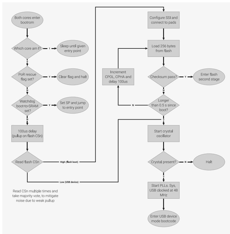
graph TD
    Start([Both cores enter bootrom]) --> CoreID{Which core am I?}
    CoreID -- 1 --> Sleep([Sleep until given entry point])
    CoreID -- 0 --> PoR{PoR rescue flag set?}
    PoR -- Y --> ClearFlag([Clear flag and halt])
    PoR -- N --> Watchdog{Watchdog boot-to-SRAM set?}
    Watchdog -- Y --> SetSP([Set SP and jump to entry point])
    Watchdog -- N --> Delay[100us delay
(pullup on flash CSn)]
    Delay --> ReadCSn{Read flash CSn}
    ReadCSn -- High (flash boot) --> ConfigSSI[Configure SSI and connect to pads]
    ReadCSn -- Low (USB device) --> StartOsc[Start crystal oscillator]
    StartOsc --> CrystalPresent{Crystal present?}
    CrystalPresent -- N --> Halt([Halt])
    CrystalPresent -- Y --> StartPLL[Start PLLs, Sys, USB clocked at 48 MHz]
    StartPLL --> EnterUSB[Enter USB device mode bootcode]
    EnterUSB --> LoadFlash[Load 256 bytes from flash]
    LoadFlash --> Checksum{Checksum pass?}
    Checksum -- Y --> EnterFlash2[Enter flash second stage]
    Checksum -- N --> TimeOut{Longer than 0.5 s since boot?}
    TimeOut -- Y --> EnterFlash2
    TimeOut -- N --> Increment[Increment CPOL, CPHA and delay 100us]
    Increment --> LoadFlash
After the hardware controlled boot sequence described in Section 2.7 , the processor controlled boot sequence starts:
- • Reset to both processors released: both enter ROM at same location
- • Processors check SIO.CPUID
- ◦ Processor 1 goes to sleep (WFE with SCR.SLEEPDEEP enabled) and remains asleep until woken by user code, via the mailbox
- ◦ Processor 0 continues executing from ROM
- • If power up event was from Rescue DP, clear this flag and
halt immediately
- ◦ The debug host (which initiated the rescue) will provide further instruction.
- • If watchdog scratch registers set to indicate pre-loaded code exists in SRAM, jump to that code
- • Check if SPI CS pin is tied low ("bootrom button"), and skip flash boot if so.
- • Set up IO muxing, pad controls on QSPI pins, and initialise Synopsys SSI for standard SPI mode
- • Issue XIP exit sequence, in case flash is still in an XIP mode and has not been power-cycled
- • Copy 256 bytes from SPI to internal SRAM (SRAM5) and check for valid CRC32 checksum
- • If checksum passes, assume what we have loaded is a valid flash second stage
- • Start executing the loaded code from SRAM (SRAM5)
- • If no valid image found in SPI after 0.5 seconds of attempting to boot, drop to USB device boot
- • USB device boot: appear as a USB Mass Storage Device
- ◦ Can program the SPI flash, or load directly into SRAM and run, by dragging and dropping an image in UF2 format.
- ◦ Also supports an extended PICOBOOT interface
2.8.1.1. Watchdog Boot
Watchdog boot allows users to install their own boot handler, and divert control away from the main boot sequence on non-POR/BOR resets. It also simplifies running code over the JTAG test interface. It recognises the following values written to the watchdog's upper scratch registers:
- • Scratch 4: magic number
0xb007c0d3 - • Scratch 5: Entry point XORed with magic
-0xb007c0d3 (0x4ff83f2d) - • Scratch 6: Stack pointer
- • Scratch 7: Entry point
If either of the magic numbers mismatch, watchdog boot does not take place. If the numbers match, the Bootrom zeroes scratch 4 before transferring control, so that the behaviour does not persist over subsequent reboots.
2.8.1.2. Flash Boot Sequence
One of the main challenges of a warm flash boot is forcing the external flash from XIP mode to a mode where it will accept standard SPI commands. There is no standard method to discontinue XIP on an unknown flash. The Bootrom provides a best-effort sequence with broad compatibility, which is as follows:
- •
CSn=1, IO[3:0]=4'b0000(via pull-downs to avoid contention), issue \( \times 32 \) clocks - •
CSn=0, IO[3:0]=4'b1111(via pull-ups to avoid contention), issue \( \times 32 \) clocks - •
CSn=1 - •
CSn=0, MOSI=1'b1(driven low-Z, all other IOs Hi-Z), issue \( \times 16 \) clocks
This is designed to miss the XIP continuation codes on Cypress, Micron and Winbond parts. If the device is already in SPI mode, it interprets this sequence as two
FFh NOP
instructions, which should be ignored.
As this is best effort only, there may be some devices which obstinately remain in XIP mode. There are then two options:
- • Use a less efficient XIP mode where each transfer has an SPI instruction prefix, so the flash device remains communicative in SPI mode.
- • Boot code installs a compatible XIP exit sequence in SRAM, and configures the watchdog such that a warm boot will jump straight into this sequence, foregoing our canned sequence.
After issuing the XIP exit sequence, the Bootrom attempts to read in the second stage from flash using standard
03h
serial read commands, which are near-universally supported. Since the Bootrom is immutable, it aims for compatibility
rather than performance.
2.8.1.3. Flash Second Stage
The flash second stage must configure the SSI and the external flash for the best possible execute-in-place performance. This includes interface width, SCK frequency, SPI instruction prefix and an XIP continuation code for address-data only modes. Generally some operation can be performed on the external flash so that it does not require an instruction prefix on each access, and will simply respond to addresses with data.
Until the SSI is correctly configured for the attached flash device, it is not possible to access flash via the XIP address window. Additionally, the Synopsys SSI can not be reconfigured at all without first disabling it. Therefore the second stage must be copied from flash to SRAM by the bootrom, and executed in SRAM.
Alternatively, the second stage can simply shadow an image from external flash into SRAM, and not configure execute-in-place.
This is the only job of the second stage. All other chip setup (e.g. PLLs, Voltage Regulator) can be performed by platform initialisation code executed over the XIP interface, once the second stage has run.
2.8.1.3.1. Checksum
The last four bytes of the image loaded from flash (which we hope is a valid flash second stage) are a CRC32 checksum of the first 252 bytes. The parameters of the checksum are:
- • Polynomial:
0x04c11db7 - • Input reflection: no
- • Output reflection: no
- • Initial value:
0xffffffff - • Final XOR:
0x00000000 - • Checksum value appears as little-endian integer at end of image
The Bootrom makes 128 attempts of approximately 4ms each for a total of approximately 0.5 seconds before giving up and dropping into USB code to load and checksum the second stage with varying SPI parameters. If it sees a checksum pass it will immediately jump into the 252-byte payload which contains the flash second stage.
2.8.2. Launching Code On Processor Core 1
As described in the introduction to Section 2.8.1 , after reset, processor core 1 "sleeps (WFE with SCR.SLEEPDEEP enabled) and remains asleep until woken by user code, via the mailbox".
If you are using the SDK then you can simply use the
multicore_launch_core1
function to launch code on processor core 1. However this section describes the procedure to launch code on processor core 1 yourself.
The procedure to start running on processor core 1 involves both cores moving in lockstep through a state machine coordinated by passing messages over the inter-processor FIFOs. This state machine is designed to be robust enough to cope with a recently reset processor core 1 which may be anywhere in its boot code, up to and including going to sleep. As result, the procedure may be performed at any point after processor core 1 has been reset (either by system reset, or explicitly resetting just processor core 1).
The following C code is the simplest way to describe the procedure:
// values to be sent in order over the FIFO from core 0 to core 1
//
// vector_table is value for VTOR register
// sp is initial stack pointer (SP)
// entry is the initial program counter (PC) (don't forget to set the thumb bit!)
const uint32_t cmd_sequence[] =
    {0, 0, 1, (uintptr_t) vector_table, (uintptr_t) sp, (uintptr_t) entry};

uint seq = 0;
do {
    uint cmd = cmd_sequence[seq];
    // always drain the READ FIFO (from core 1) before sending a 0
    if (!cmd) {
        // discard data from read FIFO until empty
        multicore_fifo_drain();
        // execute a SEV as core 1 may be waiting for FIFO space
        __sev();
    }
    // write 32 bit value to write FIFO
    multicore_fifo_push_blocking(cmd);
    // read 32 bit value from read FIFO once available
    uint32_t response = multicore_fifo_pop_blocking();
    // move to next state on correct response (echo-d value) otherwise start over
    seq = cmd == response ? seq + 1 : 0;
} while (seq < count_of(cmd_sequence));
2.8.3. Bootrom Contents
Some of the bootrom is dedicated to the implementation of the boot sequence and USB boot interfaces. There is also code in the bootrom useful to user programs. Table 163 shows the fixed memory layout of the first handful of words in the Bootrom which are instrumental in locating other content within the bootrom.
Table 163. Bootrom contents at fixed (well known) addresses
| Address | Contents | Description |
|---|---|---|
| 0x00000000 | 32-bit pointer | Initial boot stack pointer |
| 0x00000004 | 32-bit pointer | Pointer to boot reset handler function |
| 0x00000008 | 32-bit pointer | Pointer to boot NMI handler function |
| 0x0000000c | 32-bit pointer | Pointer to boot Hard fault handler function |
| 0x00000010 | 'M', 'u', 0x01 | Magic |
| 0x00000013 | byte | Bootrom version |
| 0x00000014 | 16-bit pointer | Pointer to a public function lookup table (rom_func_table) |
| 0x00000016 | 16-bit pointer | Pointer to a public data lookup table (rom_data_table) |
| 0x00000018 | 16-bit pointer | Pointer to a helper function (rom_table_lookup()) |
2.8.3.1. Bootrom Functions
The Bootrom contains a number of public functions that provide useful RP2040 functionality that might be needed in the absence of any other code on the device, as well as highly optimized versions of certain key functionality that would otherwise have to take up space in most user binaries.
These functions are normally made available to the user by the SDK, however a lower level method is provided to locate them (their locations may change with each Bootrom release) and call them directly.
Assuming the three bytes starting at address 0x00000010 are ('M', 'u', 0x01) then the three halfwords starting at offset 0x00000014 are valid.
These three values can be used to dynamically locate other functions or data within the Bootrom. The version byte at offset
0x00000013
is informational and should not be used to infer the exact location of any functions.
The following code from the SDK shows how the three 16-bit pointers are used to lookup other functions or data.
SDK: https://github.com/raspberrypi/pico-sdk/blob/master/src/rp2_common/pico_bootrom/bootrom.c Lines 12 - 19
12 void *rom_func_lookup(uint32_t code) {
13     return rom_func_lookup_inline(code);
14 }
15
16 void *rom_data_lookup(uint32_t code) {
17     return rom_data_lookup_inline(code);
18 }
The
code
parameter correspond to the
CODE
values in the tables below, and is calculated as follows:
uint32_t rom_table_code(char c1, char c2) {
    return (c2 << 8) | c1;
}
2.8.3.1.1. Fast Bit Counting / Manipulation Functions
These are optimized versions of common bit counting / manipulation functions.
In general you do not need to call these methods directly as the SDK
pico_bit_ops
library replaces the corresponding standard compiler library functions by default so that the standard functions such as
__builtin_popcount
or
__clzdi2
uses the corresponding Bootrom implementations automatically (see
pico_bit_ops
for more details).
These functions have changed in speed slightly between version 1 (V1) of the bootrom and version 2 (V2).
Table 164. Fast Bit Counting / Manipulation Functions.
| CODE | Cycles Avg V1 | Cycles Avg V2/V3 | Description |
|---|---|---|---|
| 'P', '3' | 18 | 20 | uint32_t _popcount32(uint32_t value) |
Return a count of the number of 1 bits in
value
. | |||
| 'R', '3' | 21 | 22 | uint32_t _reverse32(uint32_t value) |
Return the bits of
value
in the reverse order. | |||
| 'L', '3' | 13 | 9.6 | uint32_t _clz32(uint32_t value) |
Return the number of consecutive high order 0 bits of
value
. If
value
is zero, returns 32. | |||
| 'T', '3' | 12 | 11 | uint32_t _ctz32(uint32_t value) |
Return the number of consecutive low order 0 bits of
value
. If
value
is zero, returns 32. |
2.8.3.1.2. Fast Bulk Memory Fill / Copy Functions
These are highly optimized bulk memory fill and copy functions commonly provided by most language runtimes.
In general you do not need to call these methods directly as the SDK
pico_mem_ops
library replaces the corresponding standard ARM EABI functions by default so that the standard C library functions e.g.
memcpy
or
memset
use the Bootrom implementations automatically (see
pico_mem_ops
for more details).
Table 165. Optimized Bulk Memory Fill / Copy Functions
| CODE | Description |
|---|---|
| 'M', 'S' | uint8_t *_memset(uint8_t *ptr, uint8_t c, uint32_t n)Sets n
bytes start at
ptr
to the value
c
and returns
ptr
. |
| 'S', '4' | uint32_t *_memset4(uint32_t *ptr, uint8_t c, uint32_t n)Sets n
bytes start at
ptr
to the value
c
and returns
ptr
. Note this is a slightly more efficient variant of
_memset
that may only be used if
ptr
is word aligned. |
| 'M', 'C' | uint8_t *_memcpy(uint8_t *dest, uint8_t *src, uint32_t n)Copies n
bytes starting at
src
to
dest
and returns
dest
. The results are undefined if the regions overlap. |
| 'C', '4' | uint8_t *_memcpy44(uint32_t *dest, uint32_t *src, uint32_t n)Copies n
bytes starting at
src
to
dest
and returns
dest
. The results are undefined if the regions overlap. Note this is a slightly more efficient variant of
_memcpy
that may only be used if
dest
and
src
are word aligned. |
2.8.3.1.3. Flash Access Functions
These are low level flash helper functions.
Table 166. Flash Access Functions
| CODE | Description |
|---|---|
| 'I', 'F' | void _connect_internal_flash(void)Restore all QSPI pad controls to their default state, and connect the SSI to the QSPI pads |
| 'E', 'X' | void _flash_exit_xip(void)First set up the SSI for serial-mode operations, then issue the fixed XIP exit sequence described in Section 2.8.1.2 . Note that the bootrom code uses the IO forcing logic to drive the CS pin, which must be cleared before returning the SSI to XIP mode (e.g. by a call to _flash_flush_cache
). This function configures the SSI with a fixed SCK clock divisor of /6. |
| 'R', 'E' | void _flash_range_erase(uint32_t addr, size_t count, uint32_t block_size, uint8_t block_cmd)Erase a count
bytes, starting at
addr
(offset from start of flash). Optionally, pass a block erase command e.g.
08h
block_erase
, and the size of the block erased by this command — this function will use the larger block erase where possible, for much higher erase speed.
addr
must be aligned to a 4096-byte sector, and
count
must be a multiple of 4096 bytes. |
| 'R', 'P' | void flash_range_program(uint32_t addr, const uint8_t *data, size_t count)Program data
to a range of flash addresses starting at
addr
(offset from the start of flash) and
count
bytes in size.
addr
must be aligned to a 256-byte boundary, and
count
must be a multiple of 256. |
| 'F', 'C' | void _flash_flush_cache(void)Flush and enable the XIP cache. Also clears the IO forcing on QSPI CSn, so that the SSI can drive the flash chip select as normal. |
| 'C', 'X' | void _flash_enter_cmd_xip(void)Configure the SSI to generate a standard 03h
serial read command, with 24 address bits, upon each
XIP
access. This is a very slow XIP configuration, but is very widely supported. The debugger calls this function after performing a flash erase/programming operation, so that the freshly-programmed code and data is visible to the debug host, without having to know exactly what kind of flash device is connected. |
A typical call sequence for erasing a flash sector from user code would be:
- •
_connect_internal_flash - •
_flash_exit_xip - •
_flash_range_erase(addr, 1 << 12, 1 << 16, 0xd8) - •
_flash_flush_cache - • Either a call to
_flash_enter_cmd_xipor call into a flash second stage that was previously copied out into SRAM
Note that, in between the first and last calls in this sequence, the SSI is
not
in a state where it can handle XIP accesses, so the code that calls the intervening functions must be located in SRAM. The SDK
hardware_flash
library hides these details.
2.8.3.1.4. Debugging Support Functions
These two methods simplify the task of calling code on the device and then returning control to the debugger.
Table 167. Debugging Support Functions
| CODE | Description |
|---|---|
| 'D', 'T' | _debug_trampoline |
| Simple debugger trampoline for break-on-return. | |
This methods helps the debugger call ROM routines without setting hardware breakpoints. The function address is passed in
r7
and args are passed through
r0 ... r3
as per ABI.This method does not return but executes a BKPT #0
at the end. | |
| 'D', 'E' | _debug_trampoline_end |
This is the address of the final
BKPT #0
instruction of
debug_trampoline
. This can be compared with the program counter to detect completion of the
debug_trampoline
call. |
2.8.3.1.5. Miscellaneous Functions
These remaining functions don't fit in other categories and are exposed in the SDK via the
pico_bootrom
library (see
pico_bootrom
).
Table 168. Miscellaneous Functions
| CODE | Description |
|---|---|
| 'U', 'B' | void _reset_to_usb_boot(uint32_t gpio_activity_pin_mask, uint32_t disable_interface_mask) |
Resets the RP2040 and uses the watchdog facility to re-start in BOOTSEL mode:
|
| 'W', 'V' | _wait_for_vector |
| This is the method that is entered by core 1 on reset to wait to be launched by core 0. There are few cases where you should call this method (resetting core 1 is much better). This method does not return and should only ever be called on core 1. | |
| 'E', 'C' | deprecated |
| Do not use this function which may not be present. |
2.8.3.2. Fast Floating Point Library
The Bootrom contains an optimized single-precision floating point implementation. Additionally V2 onwards also contain an optimized double-precision float point implementation. The function pointers for each precision are kept in a table structure found via the
rom_data_lookup
table (see
Section 2.8.3.3
).
2.8.3.2.1. Implementation Details
There is always a trade-off between speed and size. Whilst the overall goal for the floating-point routines is to achieve good performance within a small footprint, the emphasis is more on improved performance for the basic operations (add, subtract, multiply, divide and square root) and more on reduced footprint for the scientific functions (trigonometric functions, logarithms and exponentials).
The IEEE single- and double-precision data formats are used throughout, but in the interests of reducing code size, input denormals are treated as zero, input NaNs are treated as infinities, output denormals are flushed to zero, and output NaNs are rendered as infinities. Only the round-to-nearest, even-on-tie rounding mode is supported. Traps are not supported.
The five basic operations return results that are always correctly rounded.
The scientific functions always return results within 1 ULP (unit in last place) of the exact result. In many cases results are better.
The scientific functions are calculated using internal fixed-point representations so accuracy (as measured in ULP error rather than in absolute terms) is poorer in situations where converting the result back to floating point entails a large normalising shift. This occurs, for example, when calculating the sine of a value near a multiple of pi, the cosine of a value near an odd multiple of pi/2, or the logarithm of a value near 1. Accuracy of the tangent function is also poorer when the result is very large. Although covering these cases is possible, it would add considerably to the code footprint, and there are few types of program where accuracy in these situations is essential.
The sine, cosine and tangent functions also only operate correctly over a limited range: \( -128 < x < +128 \) for single-precision arguments x and \( -1024 < x < +1024 \) for double-precision x. This is to avoid the need to (at least in effect) store the value of pi to high precision within the code, and hence saves code space. Accurate range reduction over a wider range of arguments can be done externally to the library if required, but again there are few situations where this would be needed.
NOTE
The SDK cos/sin functions perform this range reduction, so accept the full range of arguments, though are slower for inputs outside of these ranges.
2.8.3.2.2. Functions
These functions follow the standard ARM EABI for passing floating point values.
You do not need to call these methods directly as the SDK
pico_float
and
pico_double
libraries used by default replace the
ARM EABI Float functions
such that C/C++ level code (or indirectly code in languages such as
MicroPython
that are implemented in C) use these Bootrom functions automatically for the corresponding floating point operations.
Some of these functions do not behave exactly the same as some of the corresponding C library functions. For that reason if you are using the SDK it is strongly advised that you simply use the regular
math.h
functions or those in
pico/float.h
or
pico/double.h
and not try to call into the bootrom directly.
Note that double-precision floating point support is not present in version 1 (V1) of the bootrom, but the above mentioned
pico_double
library in the SDK will take care of pulling in any extra code needed for V1.
i NOTE
For more information on using floating point in the SDK, and real world timings (noting also that some conversion functions are re-implemented in the SDK to be faster) see floating point support .
Table 169. Single-precision Floating Point Function Table. Timings are average time in us over random (worst case) input. Functions with timing of N/A are not present in that ROM version, and the function pointer should be considered invalid. The functions (and table entries) from offset 0x54 onwards are only present in the V2 ROM.
| Offset | V1 Cycles (Avg) | V2/V3 Cycles (Avg) | Description |
|---|---|---|---|
| Functions common to all versions of the bootrom | |||
| 0x00 | 71 | 71 | float _fadd(float a, float b) |
| Return \( a + b \) | |||
| 0x04 | 74 | 74 | float _fsub(float a, float b) |
| Return \( a - b \) | |||
| 0x08 | 69 | 58 | float _fmul(float a, float b) |
| Return \( a * b \) | |||
| 0x0c | 71 | 71 | float _fdiv(float a, float b) |
| Return \( a / b \) | |||
| 0x10 | N/A | N/A | deprecated |
| Do not use this function | |||
| 0x14 | N/A | N/A | deprecated |
| Do not use this function | |||
| 0x18 | 63 | 63 | float _fsqrt(float v) |
| Return \( \sqrt{v} \) or -Infinity if \( v \) is negative. (Note V1 returns +Infinity in this case) | |||
| 0x1c | 37 | 40 | int _float2int(float v) |
Convert a float to a signed integer, rounding towards
-Infinity
, and clamping the result to lie within the range
-0x80000000
to
0x7FFFFFFF | |||
| 0x20 | 36 | 39 | int _float2fix(float v, int n) |
Convert a float to a signed fixed point integer representation where
\(
n
\)
specifies the position of the binary point in the resulting fixed point representation - e.g.
_float2fix(0.5f, 16) == 0x8000
. This method rounds towards
-Infinity
, and clamps the resulting integer to lie within the range
-0x80000000
to
0x7FFFFFFF | |||
| 0x24 | 38 | 39 | uint _float2uint(float v) |
Convert a float to an unsigned integer, rounding towards
-Infinity
, and clamping the result to lie within the range
0x00000000
to
0xFFFFFFFF | |||
| 0x28 | 38 | 38 | uint_float2ufix(float v, int n) |
Convert a float to an unsigned fixed point integer representation where
\(
n
\)
specifies the position of the binary point in the resulting fixed point representation, e.g.
_float2ufix(0.5f, 16) == 0x8000
. This method rounds towards
-Infinity
, and clamps the resulting integer to lie within the range
0x00000000
to
0xFFFFFFFF | |||
| 0x2c | 55 | 55 | float_int2float(int v) |
| Convert a signed integer to the nearest float value, rounding to even on tie | |||
| 0x30 | 53 | 53 | float_fix2float(int32_t v, int n) |
| Convert a signed fixed point integer representation to the nearest float value, rounding to even on tie. \( n \) specifies the position of the binary point in fixed point, so \( f = nearest(v / 2^n) \) | |||
| 0x34 | 54 | 54 | float_uint2float(uint32_t v) |
| Convert an unsigned integer to the nearest float value, rounding to even on tie | |||
| 0x38 | 52 | 52 | float_ufix2float(uint32_t v, int n) |
| Convert an unsigned fixed point integer representation to the nearest float value, rounding to even on tie. \( n \) specifies the position of the binary point in fixed point, so \( f = nearest(v / 2^n) \) | |||
| 0x3c | 603 | 587 | float_fcos(float angle) |
| Return the cosine of angle . angle is in radians, and must be in the range -128 to 128 | |||
| 0x40 | 593 | 577 | float_fsin(float angle) |
| Return the sine of angle . angle is in radians, and must be in the range -128 to 128 | |||
| 0x44 | 669 | 653 | float_ftan(float angle) |
| Return the tangent of angle . angle is in radians, and must be in the range -128 to 128 | |||
| 0x48 | N/A | N/A | deprecated |
| Do not use this function | |||
| 0x4c | 542 | 524 | float_fexp(float v) |
| Return the exponential value of \( v \) , i.e. so \( e^v \) | |||
| 0x50 | 810 | 789 | float_fln( float v) |
| Return the natural logarithm of \( v \) . If \( v < 0 \) return -Infinity | |||
| Functions (and table entries) present in the V2/V3 bootrom only | |||
| 0x54 | N/A | 25 | int_fcmp(float a, float b) |
Compares two floating point numbers, returning:
| |||
| 0x58 | N/A | 667 | float_fatan2(float y, float x) |
| Computes the arc tangent of \( y/x \) using the signs of arguments to determine the correct quadrant | |||
| 0x5c | N/A | 62 | float _int642float(int64_t v) |
| Convert a signed 64-bit integer to the nearest float value, rounding to even on tie | |||
| 0x60 | N/A | 60 | float _fix642float(int64_t v, int n) |
| Convert a signed fixed point 64-bit integer representation to the nearest float value, rounding to even on tie. \( n \) specifies the position of the binary point in fixed point, so \( f = nearest(v / 2^n) \) | |||
| 0x64 | N/A | 58 | float _uint642float(uint64_t v) |
| Convert an unsigned 64-bit integer to the nearest float value, rounding to even on tie | |||
| 0x68 | N/A | 57 | float _ufix642float(uint64_t v, int n) |
| Convert an unsigned fixed point 64-bit integer representation to the nearest float value, rounding to even on tie. \( n \) specifies the position of the binary point in fixed point, so \( f = nearest(v / 2^n) \) | |||
| 0x6c | N/A | 54 | _float2int64 |
Convert a float to a signed 64-bit integer, rounding towards
-Infinity
, and clamping the result to lie within the range
-0x8000000000000000
to
0x7FFFFFFFFFFFFFFF | |||
| 0x70 | N/A | 53 | _float2fix64 |
Convert a float to a signed fixed point 64-bit integer representation where
\(
n
\)
specifies the position of the binary point in the resulting fixed point representation - e.g.
_float2fix(0.5f, 16) == 0x8000
. This method rounds towards
-Infinity
, and clamps the resulting integer to lie within the range
-0x8000000000000000
to
0x7FFFFFFFFFFFFFFF | |||
| 0x74 | N/A | 42 | _float2uint64 |
Convert a float to an unsigned 64-bit integer, rounding towards
-Infinity
, and clamping the result to lie within the range
0x0000000000000000
to
0xFFFFFFFFFFFFFFF | |||
| 0x78 | N/A | 41 | _float2ufix64 |
Convert a float to an unsigned fixed point 64-bit integer representation where
\(
n
\)
specifies the position of the binary point in the resulting fixed point representation, e.g.
_float2ufix(0.5f, 16) == 0x8000
. This method rounds towards
-Infinity
, and clamps the resulting integer to lie within the range
0x0000000000000000
to
0xFFFFFFFFFFFFFFF | |||
| 0x7c | N/A | 15 | double _float2double(float v) |
| Converts a float to a double | |||
| Function present in the V3 bootrom only | |||
| 0x48 (uses previously deprecated slot) | 577 (V3 only) | float (float) _fsincos(float angle) | |
Calculates the sine and cosine of
angle
.
angle
is in radians, and must be in the range -128 to 128. The sine value is returned in register
r0
(and is thus the official function return value), the cosine value is returned in register
r1
. This method is considerably faster than calling
_fsin
and
_fcos
separately. | |||
Note that the V2/V3 bootroms contains an equivalent table of functions for double-precision floating point operations. The offsets are the same, however where there was now float there is double (and vice versa for the float<>double conversion)
Table 170. Double-precision Floating Point Function Table. Timings are average time in us over random (worst case) input. Functions with timing of N/A are not present in that ROM version, and the function pointer should be considered invalid. The functions (and table entries) from offset 0x54 onwards are only present in the V2 and V3 ROMs.
| Offset | Cycles (Avg)* | Description |
|---|---|---|
| 0x00 | 91 | double _dadd(double a, double b) |
| Return a + b | ||
| 0x04 | 95 | double _dsub(double a, double b) |
| Return a - b | ||
| 0x08 | 155 | double _dmul(double a, double b) |
| Return a * b | ||
| 0x0c | 183 | double _ddiv(double a, double b) |
| Return a / b | ||
| 0x10 | N/A | deprecated |
| Do not use this function | ||
| 0x14 | N/A | deprecated |
| Do not use this function | ||
| 0x18 | 169 | double _dsqrt(double v) |
| Return \( \sqrt{v} \) or -Infinity if v is negative. | ||
| 0x1c | 75 | int _double2int(double v) |
| Convert a double to a signed integer, rounding towards -Infinity , and clamping the result to lie within the range -0x80000000 to 0x7FFFFFFF | ||
| 0x20 | 74 | int _double2fix(double v, int n) |
Convert a double to a signed fixed point integer representation where
n
specifies the position of the binary point in the resulting fixed point representation - e.g.
_double2fix(0.5f, 16) == 0x8000
. This method rounds towards
-Infinity
, and clamps the resulting integer to lie within the range -0x80000000 to 0x7FFFFFFF | ||
| 0x24 | 63 | uint _double2uint(double v) |
| Convert a double to an unsigned integer, rounding towards -Infinity , and clamping the result to lie within the range 0x00000000 to 0xFFFFFFFF | ||
| 0x28 | 62 | uint _double2ufix(double v, int n) |
Convert a double to an unsigned fixed point integer representation where
n
specifies the position of the binary point in the resulting fixed point representation, e.g.
_double2ufix(0.5f, 16) == 0x8000
. This method rounds towards
-Infinity
, and clamps the resulting integer to lie within the range 0x00000000 to 0xFFFFFFFF | ||
| 0x2c | 69 | double _int2double(int v) |
| Convert a signed integer to the nearest double value, rounding to even on tie | ||
| 0x30 | 68 | double _fix2double(int32_t v, int n) |
| Convert a signed fixed point integer representation to the nearest double value, rounding to even on tie. n specifies the position of the binary point in fixed point, so \( f = nearest(v / 2^n) \) | ||
| 0x34 | 64 | double _uint2double(uint32_t v) |
| Convert an unsigned integer to the nearest double value, rounding to even on tie |
| Offset | Cycles (Avg)* | Description |
|---|---|---|
| 0x38 | 62 | double _ufix2double(uint32_t v, int n) |
| Convert an unsigned fixed point integer representation to the nearest double value, rounding to even on tie. \( n \) specifies the position of the binary point in fixed point, so \( f = nearest(v / 2^n) \) | ||
| 0x3c | 1617 | double _dcos(double angle) |
| Return the cosine of angle . angle is in radians, and must be in the range -1024 to 1024 | ||
| 0x40 | 1618 | double _dsin(double angle) |
| Return the sine of angle . angle is in radians, and must be in the range -1024 to 1024 | ||
| 0x44 | 1891 | double _dtan(double angle) |
| Return the tangent of angle . angle is in radians, and must be in the range -1024 to 1024 | ||
| 0x48 | N/A | deprecated |
| Do not use this function | ||
| 0x4c | 804 | double _dexp(double v) |
| Return the exponential value of \( v \) , i.e. so \( e^v \) | ||
| 0x50 | 428 | double _dln( double v) |
| Return the natural logarithm of \( v \) . If \( v < 0 \) return -Infinity | ||
| 0x54 | 39 | int _dcmp(double a, double b) |
Compares two floating point numbers, returning:
| ||
| 0x58 | 2168 | double _datan2(double y, double x) |
| Computes the arc tangent of \( y/x \) using the signs of arguments to determine the correct quadrant | ||
| 0x5c | 55 | double _int642double(int64_t v) |
| Convert a signed 64-bit integer to the nearest double value, rounding to even on tie | ||
| 0x60 | 56 | double _dix642double(int64_t v, int n) |
| Convert a signed fixed point 64-bit integer representation to the nearest double value, rounding to even on tie. \( n \) specifies the position of the binary point in fixed point, so \( f = nearest(v / 2^n) \) | ||
| 0x64 | 50 | double _uint642double(uint64_t v) |
| Convert an unsigned 64-bit integer to the nearest double value, rounding to even on tie | ||
| 0x68 | 49 | double _ufix642double(uint64_t v, int n) |
| Convert an unsigned fixed point 64-bit integer representation to the nearest double value, rounding to even on tie. \( n \) specifies the position of the binary point in fixed point, so \( f = nearest(v / 2^n) \) | ||
| 0x6c | 64 | _double2int64 |
Convert a double to a signed 64-bit integer, rounding towards
-Infinity
, and clamping the result to lie within the range
-0x8000000000000000
to
0x7FFFFFFFFFFFFFFF |
| Offset | Cycles (Avg)* | Description |
|---|---|---|
| 0x70 | 63 | _double2fix64 |
Convert a double to a signed fixed point 64-bit integer representation where
n
specifies the position of the binary point in the resulting fixed point representation - e.g.
_double2fix(0.5f, 16) == 0x8000
. This method rounds towards
-Infinity
, and clamps the resulting integer to lie within the range
-0x8000000000000000
to
0x7FFFFFFFFFFFFFFF | ||
| 0x74 | 53 | _double2uint64 |
Convert a double to an unsigned 64-bit integer, rounding towards
-Infinity
, and clamping the result to lie within the range
0x0000000000000000
to
0xFFFFFFFFFFFFFFF | ||
| 0x78 | 52 | _double2ufix64 |
Convert a double to an unsigned fixed point 64-bit integer representation where
n
specifies the position of the binary point in the resulting fixed point representation, e.g.
_double2ufix(0.5f, 16) == 0x8000
. This method rounds towards
-Infinity
, and clamps the resulting integer to lie within the range
0x0000000000000000
to
0xFFFFFFFFFFFFFFF | ||
| 0x7c | 23 | float _double2float(double v) |
| Converts a double to a float | ||
| Function present in the V3 bootrom only | ||
| 0x48 (uses previously deprecated slot) | 1718 (V3 only) | double (,double) _sincos(double angle) |
Calculates the sine and cosine of
angle
.
angle
is in radians, and must be in the range -1024 to 1024. The sine value is returned in registers
r0/r1
(and is thus the official return value), the cosine value is returned in registers
r2/r3
. This method is considerably faster than calling
_sin
and
_cos
separately. | ||
2.8.3.3. Bootrom Data
The Bootrom data table (
rom_data_table
) contains the following pointers.
Table 171. Bootrom data pointers
| CODE | Value (16-bit pointer) | Description |
|---|---|---|
| 'C', 'R' | const char *copyright_string | |
| The Raspberry Pi Trading Ltd copyright string. | ||
| 'G', 'R' | const uint32_t *git_revision | |
| The 8 most significant hex digits of the Bootrom git revision. | ||
| 'F', 'S' | fplib_start | |
The start address of the floating point library code and data. This and
fplib_end
along with the individual function pointers in
soft_float_table
can be used to copy the floating point implementation into RAM if desired. | ||
| 'S', 'F' | soft_float_table | |
| See Table 169 for the contents of this table. | ||
| 'F', 'E' | fplib_end | |
| The end address of the floating point library code and data. |
| 'S', 'D' | soft_double_table |
| This entry is only present in the V2 bootrom. See Table 170 for the contents of this table. | |
| 'P', '8' | deprecated . This entry is not present in the V2 bootrom; do not use it. |
| 'R', '8' | deprecated . This entry is not present in the V2 bootrom; do not use it. |
| 'L', '8' | deprecated . This entry is not present in the V2 bootrom; do not use it. |
| 'T', '8' | deprecated . This entry is not present in the V2 bootrom; do not use it. |
2.8.4. USB Mass Storage Interface
The Bootrom provides a standard USB bootloader that makes a writeable drive available for copying code to the RP2040 using UF2 files (see Section 2.8.4.2 ).
A UF2 file copied to the drive is downloaded and written to Flash or RAM, and the device is automatically rebooted, making it trivial to download and run code on the RP2040 using only a USB connection.
2.8.4.1. The RPI-RP2 Drive
The RP2040 appears as a standard 128MB flash drive named RPI-RP2 formatted as a single partition with FAT16. There are only ever two actual files visible on the drive specified.
- • INFO_UF2.TXT - contains a string description of the UF2 bootloader and version.
- • INDEX.HTM - redirects to information about the RP2040 device.
Any type of files may be written to the USB drive from the host, however in general these are not stored, and only appear to be so because of caching on the host side.
When a UF2 file is written to the device however, the special contents are recognized and data is written to specified locations in RAM or Flash. On the completed download of an entire valid UF2 file, the RP2040 automatically reboots to run the newly downloaded code.
 NOTE
NOTE
The INDEX.HTM file is currently redirected to https://www.raspberrypi.com/documentation/microcontrollers/
2.8.4.2. UF2 Format Details
 TIP
TIP
To generate UF2 files, use the UF2 convert functionality in picotool .
 NOTE
NOTE
Invalid UF2 files may not write at all or only write partially to RP2040 before failing. Not all operating systems notify you of disk write errors after a failed write. You can use picotool to verify that a UF2 file wrote correctly to RP2040.
- • All data destined for the device must be in a UF2 block with familyID present and set to 0xe48bff56 , and a payload_size of 256 .
- • All data must be destined for (and fit entirely within) the following memory ranges (depending on the type of binary being downloaded which is determined by the address of the first UF2 block encountered):
a. A regular flash binary
- ■
0x10000000-0x11000000Flash : All blocks must be targeted at 256 byte alignments. Writes beyond the end of physical flash will wrap back to the beginning of flash.
b. A RAM only binary
- ■
0x20000000-0x20042000Main RAM : Blocks can be positioned with byte alignment. - ■
0x15000000-0x15004000Flash Cache : (since flash is not being targeted, the Flash Cache is available for use as RAM with same properties as Main RAM ).
Image: Note icon
NOTETraditionally UF2 has only been used to write to Flash, but this is more a limitation of using the metadata-free .BIN file as the source to generate the UF2 file. RP2040 takes full advantage of the inherent flexibility of UF2 to support the full range of binaries in the richer .ELF format produced by the build to be used as the source for the UF2 file.
- • The
numBlocksmust specify a total size of the binary that fits in the regions specified above - • A change of
numBlocksor the binary type (determined by UF2 block target address) will discard the current transfer in progress. - • All data must be in blocks without the
UF2_FLAG_NOT_MAIN_FLASHmarking which relates to content to be ignored rather than Flash vs RAM.
The flash is always erased a 4kB sector at a time, so including data for only a subset of the 256-byte pages within a sector in a flash-binary
UF2
will leave the remaining 256-byte pages of the sector erased but undefined. The RP2040 bootrom will accept
UF2
binaries with such partially-filled sectors, however due to a bug (
RP2040-E14
) such binaries may not be written correctly if there is any partially-filled sector other than at the end. Most flash binaries are 4kB aligned and contiguous, and therefore it is usually only the last sector that is partially-filled. If you need to write non-aligned or non-contiguous
UF2
s to flash, then you should make sure to include a full 4kB worth of data for every sector in flash that will be written other than the last. This is handled for you automatically by the
elf2uf2
tool in the SDK version 1.3.1 onwards, which explicitly adds zero-filled pages to the appropriate
partially-filled
sectors.
A binary is considered "downloaded" when each of the
numBlocks
blocks has been seen at least once in the course of a single valid transfer. The data for a block is only written the first time in case of the host resending duplicate blocks.
After downloading a regular flash binary, a reset is performed after which the flash binary second stage (at address
0x10000000
- the start of flash) will be entered (if valid) via the bootrom.
A downloaded RAM only binary is entered by watchdog reset into the start of the binary, which is calculated as the lowest address of a downloaded block (with Main RAM considered lower than Flash Cache if both are present).
Finally it is possible for host software to temporarily disable UF2 writes via the PICOB00T interface to prevent interference with operations being performed via that interface (see below), in which case any UF2 file write in progress will be aborted.
2.8.5. USB PICOB00T Interface
The PICOB00T interface is a low level USB protocol for interacting with the RP2040 while it is in BOOTSEL mode. This interface may be used concurrently with the USB Mass Storage Interface.
It provides for flexible reading from and writing to RAM or Flash, rebooting, executing code on the device and a handful of other management functions.
Constants and structures related to the interface can be found in the SDK header https://github.com/raspberrypi/pico-sdk/blob/master/src/common/boot_picoboot_headers/include/boot_picoboot.h
2.8.5.1. Identifying The Device
A RP2040 device is recognized by the Vendor ID and Product ID in its device descriptor (shown in Table 172 ).
Table 172. RP2040
Boot Device
Descriptor
| Field | Value |
|---|---|
| bLength | 18 |
| bDescriptorType | 1 |
| bcdUSB | 1.10 |
| bDeviceClass | 0 |
| bDeviceSubClass | 0 |
| bDeviceProtocol | 0 |
| bMaxPacketSize0 | 64 |
| idVendor | 0x2e8a |
| idProduct | 0x0003 |
| bcdDevice | 1.00 |
| iManufacturer | 1 |
| iProduct | 2 |
| iSerial | 3 |
| bNumConfigurations | 1 |
2.8.5.2. Identifying The Interface
The PICOBOOT interface is recognized by the "Vendor Specific" Interface Class and the zero Interface Sub Class and Interface Protocol (shown in Table 173 ). Note that you should not rely on the interface number, as that is dependent on whether the device is also exposing the Mass Storage Interface. Note also that the device equally may not be exposing the PICOBOOT interface at all, so you should not assume it is present.
Table 173. PICOBOOT
Interface Descriptor
| Field | Value |
|---|---|
| bLength | 9 |
| bDescriptorType | 4 |
| bInterfaceNumber | varies |
| bAlternateSetting | 0 |
| bNumEndpoints | 2 |
| bInterfaceClass | 0xff (vendor specific) |
| bInterfaceSubClass | 0 |
| bInterfaceProtocol | 0 |
| iInterface | 0 |
2.8.5.3. Identifying The Endpoints
The PICOBOOT interface provides a single BULK OUT and a single BULK IN endpoint. These can be identified by their direction and type. You should not rely on endpoint numbers.
2.8.5.4. PICOBOOT Commands
The two bulk endpoints are used for sending commands and retrieved successful command results. All commands are exactly 32 bytes (see Table 174 ) and sent to the BULK OUT endpoint.
Table 174. PICOBOOT Command Definition
| line_number | code | comment |
|---|---|---|
| exactly 32 bytes (see | Table 174) | and sent to the BULK OUT endpoint. |
| Table 174. PICOBOOT Offset | Name | Description |
| Command Definition 0x00 | dMagic | The value 0x431fd10b |
| 0x04 | dToken | A user provided token to identify this request by |
| 0x08 | bCmdId | The ID of the command. Note that the top bit indicates data transfer direction |
| 0x09 | bCmdSize | (0x80 = IN) Number of bytes of valid data in the args field |
| 0x0a | reserved | 0x0000 |
| 0x0c | dTransferLength | The number of bytes the host expects to send or receive over the bulk channel |
| 0x10 | args | 16 bytes of command specific data padded with zeros |
| via the GET_COMMAND_STATUS | request (see Section 2.8.5.5.2 ). | |
| Following the initial 32 byte packet, if | dTranferLength is non-zero, then that many bytes are transferred over the bulk | |
| pipe and the command is completed with an empty packet in the opposite direction. If | dTransferLength is zero then | |
| The following commands are supported (note common fields | dMagic, dToken, reserved are omitted for clarity) | |
| Table 175. PICOBOOT Offset | Name | Value / Description |
| Exclusive access command structure 0x08 | bCmdId | 0x01 (EXCLUSIVE_ACCESS) |
| 0x09 | bCmdSize | 0x01 |
| 0x0c | dTransferLength | 0x00000000 |
| 0x10 | bExclusive | NOT_EXCLUSIVE (0) No restriction on USB Mass Storage operation EXCLUSIVE (1) |
| see them as write protect failures, but in any case any active UF2 download will be aborted) EXCLUSIVE_AND_EJECT Lock the USB Mass Storage Interface out by | ||
| Table 176. PICOBOOT Offset | Name Value / Description | |
| command structure Reboot access 0x08 | bCmdId 0x02 (REBOOT) | |
| 0x09 | bCmdSize 0x0c |
If a command sent is invalid or not recognized, the bulk endpoints will be stalled. Further information will be available via the GET_COMMAND_STATUS request (see Section 2.8.5.5.2 ).
Following the initial 32 byte packet, if dTransferLength is non-zero, then that many bytes are transferred over the bulk pipe and the command is completed with an empty packet in the opposite direction. If dTransferLength is zero then command success is indicated by an empty IN packet.
The following commands are supported (note common fields dMagic , dToken , reserved are omitted for clarity)
2.8.5.4.1. EXCLUSIVE_ACCESS (0x01)
Claim or release exclusive access for writing to the RP2040 over USB (versus the Mass Storage Interface)
Table 175. PICOBOOT Exclusive access command structure
2.8.5.4.2. REBOOT (0x02)
Reboots the RP2040 out of BOOTSEL mode. Note that BOOTSEL mode might be re-entered if rebooting to flash and no valid second stage bootloader is found.
Table 176. PICOBOOT Reboot access command structure
| 0x0c | dTransferLength | 0x00000000 |
| 0x10 | dPC | The address to start executing from. Valid values are: |
| 0x00000000 Reboot via the standard Flash boot mechanism | ||
| RAM address Reboot via watchdog and start executing at the specified address in RAM | ||
| 0x14 | dSP | Initial stack pointer post reboot (only used if booting into RAM) |
| 0x18 | dDelayMS | Number of milliseconds to delay prior to reboot |
2.8.5.4.3. FLASH_ERASE (0x03)
Erases a contiguous range of flash sectors.
Table 177. PICOB00T
Flash erase command structure
| Offset | Name | Value / Description |
|---|---|---|
| 0x08 | bCmdId | 0x03 (FLASH_ERASE) |
| 0x09 | bCmdSize | 0x08 |
| 0x0c | dTransferLength | 0x00000000 |
| 0x10 | dAddr | The address in flash to erase, starting at this location. This must be sector (4kB) aligned |
| 0x14 | dSize | The number of bytes to erase. This must be an exact multiple number of sectors (4kB) |
2.8.5.4.4. READ (0x84)
Read a contiguous memory (Flash or RAM or ROM) range from the RP2040
Table 178. PICOB00T
Read memory command (Flash, RAM, ROM) structure
| Offset | Name | Value / Description |
|---|---|---|
| 0x08 | bCmdId | 0x84 (READ) |
| 0x09 | bCmdSize | 0x08 |
| 0x0c | dTransferLength | Must be the same as dSize |
| 0x10 | dAddr | The address to read from. May be in Flash or RAM or ROM |
| 0x14 | dSize | The number of bytes to read |
2.8.5.4.5. WRITE (0x05)
Writes a contiguous memory range of memory (Flash or RAM) on the RP2040.
Table 179. PICOB00T
Write memory command (Flash, RAM) structure
| Offset | Name | Value / Description |
|---|---|---|
| 0x08 | bCmdId | 0x05 (WRITE) |
| 0x09 | bCmdSize | 0x08 |
| 0x0c | dTransferLength | Must be the same as dSize |
| Offset | Name | Value / Description |
|---|---|---|
| 0x10 | dAddr | The address to write from. May be in Flash or RAM, however must be page (256 byte) aligned if in Flash. Note the flash must be erased first or the results are undefined. |
| 0x14 | dSize | The number of bytes to write. If writing to flash and the size is not an exact multiple of pages (256 bytes) then the last page is zero-filled to the end. |
2.8.5.4.6. EXIT_XIP (0x06)
Exit Flash XIP mode. This first initialises the SSI for serial transfers, and then issues the XIP exit sequence given in Section 2.8.1.2 , to attempt to make the flash responsive to standard serial SPI commands. The SSI is configured with a fixed clock divisor of /6, so the USB bootloader will drive SCLK at 8MHz.
Table 180. PIC0BOOT
Exit Execute in place
(XIP) command
structure
| Offset | Name | Value / Description |
|---|---|---|
| 0x08 | bCmdId | 0x06 (EXIT_XIP) |
| 0x09 | bCmdSize | 0x00 |
| 0x0c | dTransferLength | 0x00000000 |
2.8.5.4.7. ENTER_XIP (0x07)
Enter Flash XIP mode. This configures the SSI to issue a standard 03h serial read command, with 24 address clocks and 32 data clocks, for every XIP access. This is a slow but very widely supported way to read flash. The intent of this function is to make flash easily accessible (i.e. just access addresses in the 0x10..... segment) without having to know the details of exactly what kind of flash is connected. This mode is suitable for executing code from flash, but is much slower than e.g. QSPI XIP access.
Table 181. PIC0BOOT
Enter Execute in place
(XIP) command
| Offset | Name | Value / Description |
|---|---|---|
| 0x08 | bCmdId | 0x07 (ENTER_XIP) |
| 0x09 | bCmdSize | 0x00 |
| 0x0c | dTransferLength | 0x00000000 |
2.8.5.4.8. EXEC (0x08)
Executes a function on the device. This function takes no arguments and returns no results, so it must communicate via RAM. Execution of this method will block any other commands as well as Mass Storage Interface UF2 writes, so should only be used in exclusive mode and with extreme care (and it should save and restore registers as per the ARM EABI). This method is called from a regular (non-IRQ) context, and has a very limited stack, so the function should use its own.
Table 182. PIC0BOOT
Execute function on
device command
structure
| Offset | Name | Value / Description |
|---|---|---|
| 0x08 | bCmdId | 0x08 (EXEC) |
| 0x09 | bCmdSize | 0x04 |
| 0x0c | dTransferLength | 0x00000000 |
| 0x10 | dAddr | Function address to execute at (a thumb bit will be added for you since you will have forgotten). |
2.8.5.4.9. VECTORIZE_FLASH (0x09)
Requests that the vector table of flash access functions used internally by the Mass Storage and PICOBOOT interfaces be copied into RAM, such that the method implementations can be replaced with custom versions (For example, if the board uses flash that does not support standard commands)
Table 183. PICOBOOT
Vectorise flash
command structure
| Offset | Name | Value / Description |
|---|---|---|
| 0x08 | bCmdId | 0x09 (VECTORIZE_FLASH) |
| 0x09 | bCmdSize | 0x04 |
| 0x0c | dTransferLength | 0x00000000 |
| 0x10 | dAddr | Pointer to where to place vector table in RAM |
Flash function vector table
struct {
    uint32_t size; // 28
    uint32_t (*do_flash_enter_cmd_xip)();
    uint32_t (*do_flash_exit_xip)();
    uint32_t (*do_flash_erase_sector)();
    uint32_t (*do_flash_erase_range)(uint32_t addr, uint32_t size);
    uint32_t (*do_flash_page_program)(uint32_t addr, uint8_t *data);
    uint32_t (*do_flash_page_read)(uint32_t addr, uint8_t *data);
};
These methods have the same signature and arguments as the corresponding flash access functions in the bootrom (see Section 2.8.3.1.3 ).
Note that the host must subsequently update the RAM copy of this table via an EXEC command running on the RP2040 as any write to RAM from the host via a PICOBOOT WRITE that overlaps this (now active in RAM) vector table will cause a reset to the use of the default ROM Flash function vector table.
2.8.5.5. Control Requests
The following requests are sent to the interface via the default control pipe.
2.8.5.5.1. INTERFACE_RESET (0x41)
The host sends this control request to reset the PICOBOOT interface. This command:
- • Clears the HALT condition (if set) on each of the bulk endpoints
- • Aborts any in-process PICOBOOT or Mass Storage transfer and any flash write (this method is the only way to kill a stuck flash transfer).
- • Clears the previous command result
- • Removes EXCLUSIVE_ACCESS and remounts the Mass Storage drive if it was ejected due to exclusivity.
Table 184. PICOBOOT
Reset PICOBOOT
interface control
| bmRequestType | bRequest | wValue | wIndex | wLength | Data |
|---|---|---|---|---|---|
| 01000001b | 01000001b | 0000h | Interface | 0000h | none |
This command responds with an empty packet on success.
2.8.5.5.2. GET_COMMAND_STATUS (0x42)
Retrieve the status of the last command (which may be a command still in progress). Successful completion of a PICOBOOT Protocol Command is acknowledged over the bulk pipe, however if the operation is still in progress or has failed (stalling the bulk pipe), then this method can be used to determine the operation’s status.
Table 185. PICOBOOT
Get last command
status control
| bmRequestType | bRequest | wValue | wIndex | wLength | Data |
|---|---|---|---|---|---|
| 11000001b | 01000010b | 0000h | Interface | 0000h | none |
The command responds with the following 16 byte response
Table 186. PICOBOOT
Get last command
status control
response
| Offset | Name | Description | |
|---|---|---|---|
| 0x00 | dToken | The user token specified with the command | |
| 0x04 | dStatusCode | OK (0) | The command completed successfully (or is in still in progress) |
| UNKNOWN_CMD (1) | The ID of the command was not recognized | ||
| INVALID_CMD_LENGTH (2) | The length of the command request was incorrect | ||
| INVALID_TRANSFER_LENGTH (3) | The data transfer length was incorrect given the command | ||
| INVALID_ADDRESS (4) | The address specified was invalid for the command type; i.e. did not match the type Flash/RAM that the command was expecting | ||
| BAD_ALIGNMENT (5) | The address specified was not correctly aligned according to the requirements of the command | ||
| INTERLEAVED_WRITE (6) | A Mass Storage Interface UF2 write has interfered with the current operation. The command was abandoned with unknown status. Note this will not happen if you have exclusive access. | ||
| REBOOTING (7) | The device is in the process of rebooting, so the command has been ignored. | ||
| UNKNOWN_ERROR (8) | Some other error occurred. | ||
| 0x08 | bCmdId | The ID of the command | |
| 0x09 | bInProgress | 1 if the command is still in progress | 0 otherwise |
| 0x0a | reserved | (6 zero bytes) | |
2.9. Power Supplies
RP2040 requires five separate power supplies. However, in most applications, several of these can be combined and connected to a single power source. In a typical application, only a single 3.3V supply will be required. See Section 2.9.7.1, “Single 3.3V Supply” .
The power supplies and a number of potential power supply schemes are described in the following sections. Detailed power supply parameters are provided in Section 5.6, “Power Supplies” .
2.9.1. Digital IO Supply (IOVDD)
IOVDD supplies the chip's digital IO, and should be powered at a nominal voltage between 1.8V and 3.3V. The supply voltage sets the external signal level for the digital IO and should be chosen based on the signal level required. See Section 5.5.3, "Pin Specifications" for details. All digital IOs share the same power supply and operate at the same signal level.
IOVDD should be decoupled with a 100nF capacitor close to each of the chip's IOVDD pins.
 CAUTION
If the digital IO is powered at a nominal 1.8V, the IO input thresholds should be adjusted via the VOLTAGE_SELECT register. By default, the IO input thresholds are valid when the digital IO is powered at a nominal voltage between 2.5V and 3.3V. See Section 2.19, "GPIO" for details. Powering the IO at 1.8V with input thresholds set for a 2.5V to 3.3V supply is a safe operating mode, but will result in input thresholds that do not meet specification. Powering the IO at voltages greater than a nominal 1.8V with input thresholds set for a 1.8V supply may result in damage to the chip.
2.9.2. Digital Core Supply (DVDD)
DVDD supplies the chip's core digital logic, and should be powered at a nominal 1.1V. A dedicated on-chip voltage regulator is provided to allow DVDD to be generated from the digital IO supply (IOVDD) or another nominally 1.8V to 3.3V supply. The connection between the output pin of the on-chip regulator (VREG_VOUT) and the DVDD supply pins is made off-chip, allowing DVDD to be powered from an off-chip power source if required.
DVDD should be decoupled with a 100nF capacitor close to each of the chip's DVDD pins.
2.9.3. On-Chip Voltage Regulator Input Supply (VREG_VIN)
VREG_VIN is the input supply for the on-chip voltage regulator. It should be powered at a nominal voltage between 1.8V and 3.3V. To reduce the number of external power supplies, VREG_VIN can use the same power source as the digital IO supply (IOVDD).
A 1µF capacitor should be connected between VREG_VIN and ground close to the chip's VREG_VIN pin.
 CAUTION
VREG_VIN also powers the chip's power-on reset and brown-out detection blocks, so it must be powered even if the on-chip voltage regulator is not used.
For more details on the on-chip voltage regulator see Section 2.10, "Core Supply Regulator" .
2.9.4. USB PHY Supply (USB_VDD)
USB_VDD supplies the chip's USB PHY, and should be powered at a nominal 3.3V. To reduce the number of external power supplies, USB_VDD can use the same power source as the digital IO supply (IOVDD), assuming IOVDD is also powered at 3.3V. If IOVDD is not powered at 3.3V, a separate 3.3V supply will be required for the USB PHY, see Section 2.9.7.3, "1.8V Digital IO with Functional USB and ADC" . In applications where the USB PHY is never used, USB_VDD can be tied to any supply with a nominal voltage between 1.8V and 3.3V. See Section 2.9.7.4, "Single 1.8V Supply" for an example. USB_VDD should not be left unconnected.
USB_VDD should be decoupled with a 100nF capacitor close to the chip's USB_VDD pin.
2.9.5. ADC Supply (ADC_AVDD)
ADC_AVDD supplies the chip's Analogue to Digital Converter (ADC). It can be powered at a nominal voltage between 1.8V and 3.3V, but the performance of the ADC will be compromised at voltages below 2.97V. To reduce the number of external power supplies, ADC_AVDD can use from the same power source as the digital IO supply (IOVDD).
i NOTE
It is safe to supply ADC_AVDD at a higher or lower voltage than IOVDD, e.g. to power the ADC at 3.3V, for optimum performance, while supporting 1.8V signal levels on the digital IO. But the voltage on the ADC analogue inputs must not exceed IOVDD, e.g. if IOVDD is powered at 1.8V, the voltage on the ADC inputs should be limited to 1.8V. Voltages greater than IOVDD will result in leakage currents through the ESD protection diodes. See Section 5.5.3, "Pin Specifications" for details.
ADC_AVDD should be decoupled with a 100nF capacitor close to the chip's ADC_AVDD pin.
2.9.6. Power Supply Sequencing
RP2040's power supplies may be powered up or down in any order. However, small transient currents may flow in the ADC supply (ADC_AVDD) if it is powered up before, or powered down after, the digital core supply (DVDD). This will not damage the chip, but can be avoided by powering up DVDD before or at the same time as ADC_AVDD, and powering down DVDD after or at the same time as ADC_AVDD. In the most common power supply scheme, where the chip is powered from a single 3.3V supply, DVDD will be powered up shortly after ADC_AVDD due to the startup time of the on-chip voltage regulator. This is acceptable behaviour. See Section 2.9.7.1, "Single 3.3V Supply" .
2.9.7. Power Supply Schemes
2.9.7.1. Single 3.3V Supply
In most applications, RP2040 will be powered from a single 3.3V supply, as shown in Figure 16 . The digital IO (IOVDD), USB PHY (USB_VDD) and ADC (ADC_AVDD) will be powered directly from the 3.3V supply, and the 1.1V digital core supply (DVDD) will be regulated from the 3.3V supply by the on-chip voltage regulator. Note that the regulator output pin (VREG_VOUT) must be connected to the chip's DVDD pins off-chip.
For more details on the on-chip voltage regulator see Section 2.10, "Core Supply Regulator" .
Figure 16. powering the chip from a single 3.3V supply (simplified diagram omitting decoupling components)
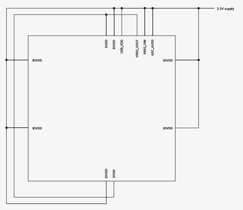
The diagram shows a central RP2040 chip with several pins connected to a single 3.3V supply. The connections are as follows:
-
DVDD
: Connected to the 3.3V supply.
-
IOVDD
: Multiple pins connected to the 3.3V supply.
-
USB_VDD
: Connected to the 3.3V supply.
-
VREG_VOUT
: Connected to the 3.3V supply.
-
VREG_VIN
: Connected to the 3.3V supply.
-
ADC_AVDD
: Connected to the 3.3V supply.
-
DVDD
(bottom): Connected to the 3.3V supply.
-
IOVDD
(bottom): Connected to the 3.3V supply.
The 3.3V supply is represented by a horizontal line at the top of the diagram.
2.9.7.2. External Core Supply
The digital core (DVDD) can be powered directly from an external 1.1V supply, rather than from the on-chip regulator, as shown in Figure 17. This approach may make sense if a suitable external regulator is available elsewhere in the system, or for low power applications where an efficient switched-mode regulator could be used instead of the less efficient linear on-chip voltage regulator.
If an external core supply is used, the output of on-chip voltage regulator (VREG_VOUT) should be left unconnected. However, power must still be provided to the regulator input (VREG_VIN) to supply the chip’s power-on reset and brown-out detection blocks. The on-chip voltage regulator will power-on as soon as VREG_VIN is available, but can be shutdown under software control once the chip is out of reset. See Section 2.10, “Core Supply Regulator” for details.
Figure 17. using an external core supply
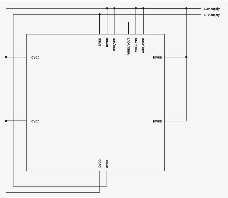
The diagram shows the same RP2040 chip as Figure 16, but with an additional 1.1V supply. The connections are:
-
DVDD
: Connected to the 1.1V supply.
-
IOVDD
: Multiple pins connected to the 3.3V supply.
-
USB_VDD
: Connected to the 3.3V supply.
-
VREG_VOUT
: Left unconnected.
-
VREG_VIN
: Connected to the 3.3V supply.
-
ADC_AVDD
: Connected to the 3.3V supply.
-
DVDD
(bottom): Connected to the 1.1V supply.
-
IOVDD
(bottom): Connected to the 3.3V supply.
The 3.3V supply is represented by a horizontal line at the top, and the 1.1V supply is represented by a horizontal line below it.
2.9.7.3. 1.8V Digital IO with Functional USB and ADC
Applications with digital IO signal levels less than 3.3V will require a separate 3.3V supply for the USB PHY and ADC, as the USB PHY does not meet specification at voltages below 3.135V and ADC performance is compromised at voltages below 2.97V. Figure 18 shows an example application with the digital IO (IOVDD) powered at 1.8V and a separate 3.3V supply for the USB PHY (USB_VDD) and ADC (ADC_AVDD). In this example, the voltage regulator input (VREG_VIN) is connected to the 1.8V supply, though it could equally have been connected to the 3.3V supply. Connecting it to the 1.8V supply will reduce overall power consumption if the 1.8V supply is generated by an efficient switched-mode regulator.
Figure 18. supporting 1.8V IO while using USB and the ADC
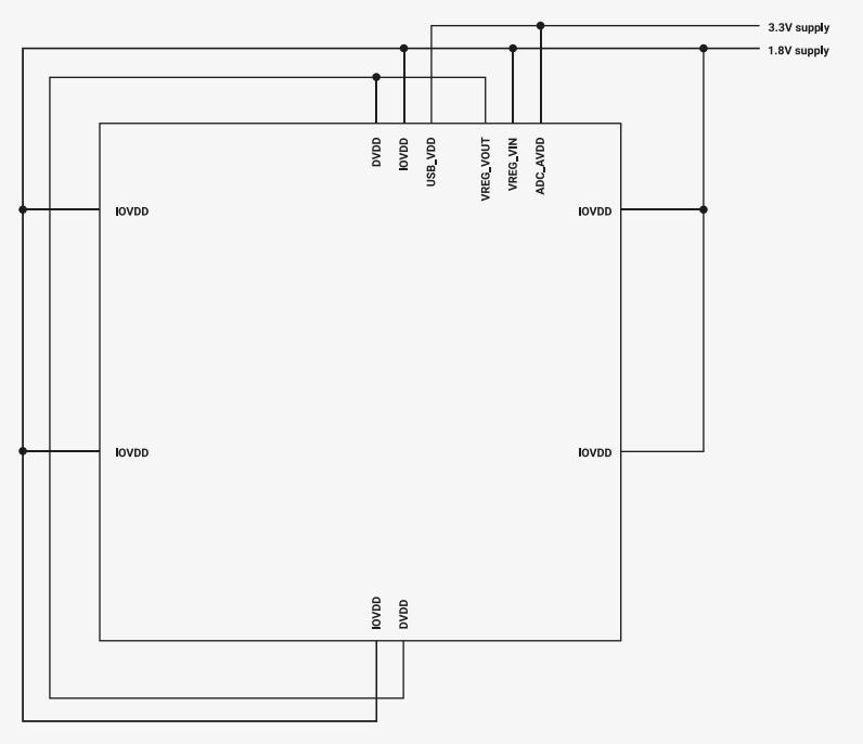
2.9.7.4. Single 1.8V Supply
If a functional USB PHY and optimum ADC performance are not required, RP2040 can be powered from a single supply of less than 3.3V. Figure 19 shows an example with a single 1.8V supply. In this example, the core supply (DVDD) is regulated from the 1.8V supply by the on-chip voltage regulator.
Figure 19. powering
the chip from a single
1.8V supply
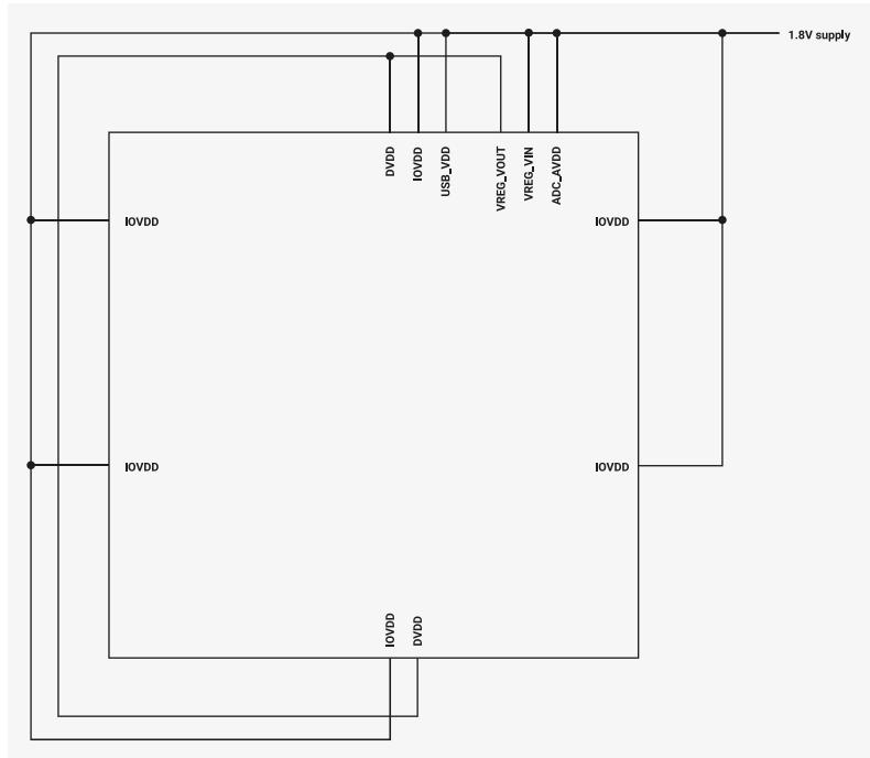
2.10. Core Supply Regulator
RP2040 includes an on-chip voltage regulator, allowing the digital core supply (DVDD) to be generated from an external, nominally 1.8V to 3.3V, power supply. In most cases, the regulator's input supply will share an external power source with the chip's digital IO supply IOVDD, simplifying the overall power supply requirements.
To allow the chip to start up, the voltage regulator is enabled by default and will power-on as soon as its input supply is available. Once the chip is out of reset, the regulator can be disabled, placed into a high impedance state, or have its output voltage adjusted, under software control. The output voltage can be set in the range 0.80V to 1.30V in 50mV steps, but is set to a nominal 1.1V at initial power-on, or after a reset event. The voltage regulator can supply up to 100mA.
Although intended to provide the chip's digital core supply (DVDD), the voltage regulator can be used for other purposes if DVDD is powered directly from an external power supply.
2.10.1. Application Circuit
Figure 20. voltage regulator application circuit
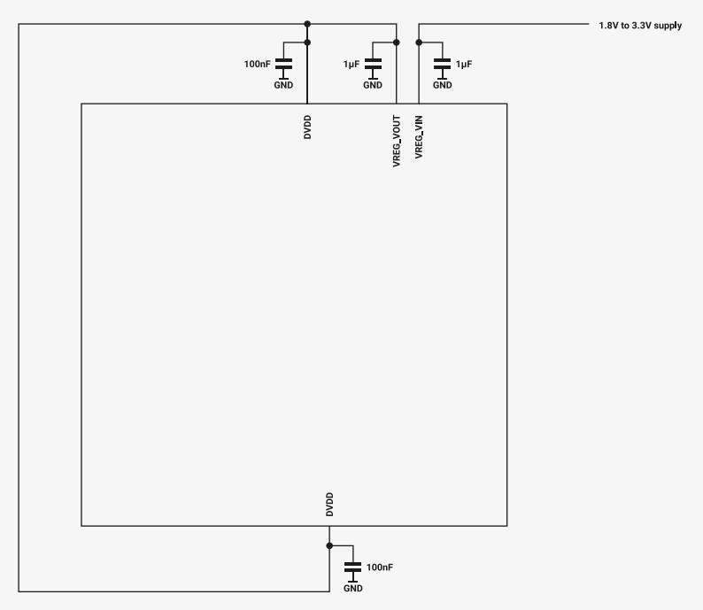
The regulator must have 1µF capacitors placed close to its input (VREG_VIN) and output (VREG_VOUT) pins.
2.10.2. Operating Modes
The voltage regulator operates in one of three modes. The mode to be used being selected by writing to the EN and HIZ fields in the VREG register, as shown in Table 187. At initial power-on, or following a reset event, the voltage regulator will be in Normal Operation mode.
Table 187. Voltage Regulator Mode Select
| Mode | EN | HIZ |
|---|---|---|
| Normal Operation a | 1 | 0 |
| High Impedance | 1 | 1 |
| Shutdown | 0 | X |
a the voltage regulator will be in normal mode at initial power-on or following a reset event
2.10.2.1. Normal Operation Mode
In Normal Operation mode, the voltage regulator’s output is in regulation at the selected voltage, and the regulator is able to supply power.
2.10.2.2. High Impedance Mode
In High Impedance mode, the voltage regulator is disabled and its output pin (VREG_VOUT) is set to a high impedance state. In this mode, the regulator’s power consumption is minimised. This mode allows a load connected to VREG_VOUT to be powered from a power source other than the on-chip regulator. This could allow, for example, the load to be initially powered from the on-chip voltage regulator, and then switched to an external regulator under software control. The external regulator would also need to support a high impedance mode, with only one regulator supplying the load at a time. The supply voltage is maintained by the regulator’s output capacitor during the brief period when both regulators are in high impedance mode.
2.10.2.3. Shutdown Mode
In Shutdown mode, the voltage regulator is disabled, power consumption is minimized and the regulator's output pin (VREG_VOUT) is pulled to 0V.
Shutdown mode is only useful if the voltage regulator is not providing the RP2040's digital core supply (DVDD). If the regulator is supplying DVDD, and brown-out detection is enabled, entering shutdown mode will cause a reset event and the voltage regulator will return to normal mode. If brown-out detection isn't enabled, the voltage regulator will shut down and will remain in shutdown mode until its input supply (VREG_VIN) is power cycled.
2.10.3. Output Voltage Select
The required output voltage can be selected by writing to the VSEL field in the VREG register. The voltage regulator's output voltage can be set in the range 0.80V to 1.30V in 50mV intervals. The regulator output voltage is set to 1.1V at initial power-on or following a reset event. For details, see the VREG register description.
Note that RP2040 may not operate reliably with its digital core supply (DVDD) outside of operating conditions (see Section 5.6 ); it is recommended to set the regulator to 1.10V for most applications.
2.10.4. Status
The VREG register contains a single status field, ROK , which indicates whether the voltage regulator's output is being correctly regulated.
At power on, ROK remains low until the regulator has started up and the output voltage reaches the ROK assertion threshold ( ROK TH.ASSERT ). It then remains high until the voltage drops below the ROK deassertion threshold ( ROK TH.DEASSERT ), remaining low until the output voltage is above the assertion threshold again. ROK TH.ASSERT is nominally 90% of the selected output voltage, 0.99V if the selected output voltage is 1.1V, and ROK TH.DEASSERT is nominally 87% of the selected output voltage, 0.957V if the selected output voltage is 1.1V.
Note that adjusting the output voltage to a higher voltage will cause ROK to go low until the assertion threshold for the higher voltage is reached. ROK will also go low if the regulator is placed in high impedance mode.
2.10.5. Current Limit
The voltage regulator includes a current limit to prevent the load current exceeding the maximum rated value. The output voltage will not be regulated and will drop below the selected value when the current limit is active.
2.10.6. List of Registers
The voltage regulator shares a register address space with the chip-level reset subsystem. The registers for both subsystems are listed here. Only, the VREG register is part of the voltage register subsystem. The BOD and CHIP_RESET registers are part of the chip-level reset subsystem. The shared address space is referred to as vreg_and_chip_reset elsewhere in this document.
The VREG_AND_CHIP_RESET registers start at a base address of 0x40064000 (defined as VREG_AND_CHIP_RESET_BASE in SDK).
Table 188. List of VREG_AND_CHIP_RESET registers
| Offset | Name | Info |
|---|---|---|
| 0x0 | VREG | Voltage regulator control and status |
| 0x4 | BOD | brown-out detection control |
| 0x8 | CHIP_RESET | Chip reset control and status |
VREG_AND_CHIP_RESET: VREG Register
Offset: 0x0
Description
Voltage regulator control and status
Table 189. VREG Register
| Bits | Description | Type | Reset |
|---|---|---|---|
| 31:13 | Reserved. | - | - |
| 12 | ROK
: regulation status 0=not in regulation, 1=in regulation | RO | 0x0 |
| 11:8 | Reserved. | - | - |
| 7:4 | VSEL
: output voltage select 0000 to 0101 - 0.80V 0110 - 0.85V 0111 - 0.90V 1000 - 0.95V 1001 - 1.00V 1010 - 1.05V 1011 - 1.10V (default) 1100 - 1.15V 1101 - 1.20V 1110 - 1.25V 1111 - 1.30V | RW | 0xb |
| 3:2 | Reserved. | - | - |
| 1 | HIZ
: high impedance mode select 0=not in high impedance mode, 1=in high impedance mode | RW | 0x0 |
| 0 | EN
: enable 0=not enabled, 1=enabled | RW | 0x1 |
VREG_AND_CHIP_RESET: BOD Register
Offset: 0x4
Description
brown-out detection control
Table 190. BOD Register
| Bits | Description | Type | Reset |
|---|---|---|---|
| 31:8 | Reserved. | - | - |
| Bits | Description | Type | Reset |
|---|---|---|---|
| 7:4 | VSEL
: threshold select 0000 - 0.473V 0001 - 0.516V 0010 - 0.559V 0011 - 0.602V 0100 - 0.645V 0101 - 0.688V 0110 - 0.731V 0111 - 0.774V 1000 - 0.817V 1001 - 0.860V (default) 1010 - 0.903V 1011 - 0.946V 1100 - 0.989V 1101 - 1.032V 1110 - 1.075V 1111 - 1.118V | RW | 0x9 |
| 3:1 | Reserved. | - | - |
| 0 | EN
: enable 0=not enabled, 1=enabled | RW | 0x1 |
VREG_AND_CHIP_RESET: CHIP_RESET Register
Offset: 0x8
Description
Chip reset control and status
Table 191.
CHIP_RESET Register
| Bits | Description | Type | Reset |
|---|---|---|---|
| 31:25 | Reserved. | - | - |
| 24 | PSM_RESTART_FLAG : This is set by psm_restart from the debugger. Its purpose is to branch bootcode to a safe mode when the debugger has issued a psm_restart in order to recover from a boot lock-up. In the safe mode the debugger can repair the boot code, clear this flag then reboot the processor. | WC | 0x0 |
| 23:21 | Reserved. | - | - |
| 20 | HAD_PSM_RESTART : Last reset was from the debug port | RO | 0x0 |
| 19:17 | Reserved. | - | - |
| 16 | HAD_RUN : Last reset was from the RUN pin | RO | 0x0 |
| 15:9 | Reserved. | - | - |
| 8 | HAD_POR : Last reset was from the power-on reset or brown-out detection blocks | RO | 0x0 |
| 7:0 | Reserved. | - | - |
2.10.7. Detailed Specifications
Table 192. Voltage Regulator Detailed Specifications
| Parameter | Description | Min | Typ | Max | Units |
|---|---|---|---|---|---|
| \( V_{VREG\_VIN} \) | input supply voltage | 1.63 | 1.8 - 3.3 | 3.63 | V |
| \( \Delta V_{VREG\_VOUT} \) | output voltage variation | -3 | +3 | % of selected output voltage | |
| \( I_{MAX} \) | output current | 100 | mA | ||
| \( I_{LIMIT} \) | current limit | 150 | 350 | 450 | mA |
| \( ROK_{TH.ASSERT} \) | ROK assertion threshold | 87 | 90 | 93 | % of selected output voltage |
| \( ROK_{TH.DEASSERT} \) | ROK deassertion threshold | 84 | 87 | 90 | % of selected output voltage |
| \( t_{POWER-ON}^a \) | power-up time | 275 | 350 | \( \mu s \) |
a values will vary with load current and capacitance on VREG_VOUT. Conditions: EN = 1, load current = 0mA, VREG_VIN ramps up in 100 \( \mu s \)
2.11. Power Control
RP2040 provides a range of options for reducing dynamic power:
- • Top-level clock gating of individual peripherals and functional blocks
- • Automatic control of top-level clock gates based on processor sleep state
- • On-the-fly changes to system clock frequency or system clock source (e.g. switch to internal ring oscillator, and disable PLLs and crystal oscillator)
- • Zero-dynamic-power DORMANT state, waking on GPIO event or RTC IRQ
All digital logic on RP2040 is in a single core power domain. The following options are available for static power reduction:
- • Placing memories into state-retaining power down state
- • Power gating on peripherals that support this, e.g. ADC, temperature sensor
2.11.1. Top-level Clock Gates
Each clock domain (for example, the system clock) may drive a large number of distinct hardware blocks, not all of which may be required at once. To avoid unnecessary power dissipation, each individual endpoint of each clock (for example, the UART system clock input) may be disabled at any time.
Enabling and disabling a clock gate is glitch-free. If a peripheral clock is temporarily disabled, and subsequently re-enabled, the peripheral will be in the same state as prior to the clock being disabled. No reset or reinitialisation should be required.
Clock gates are controlled by two sets of registers: the WAKE_ENx registers (starting at WAKE_EN0 ) and SLEEP_ENx registers (starting at SLEEP_EN0 ). These two sets of registers are identical at the bit level, each possessing a flag to control each clock endpoint. The WAKE_EN registers specify which clocks are enabled whilst the system is awake, and the SLEEP_ENx registers select which clocks are enabled while the processor is in the SLEEP state ( Section 2.11.2 ).
The two Cortex-M0+ processors do not have externally-controllable clock gates. Instead, the processors gate the clocks of their subsystems autonomously, based on execution of WFI / WFE instructions, and external Event and IRQ signals.
2.11.2. SLEEP State
RP2040 enters the SLEEP state when all of the following are true:
- • Both processors are asleep (e.g. in a WFE or WFI instruction)
- • The system DMA has no outstanding transfers on any channel
RP2040 exits the SLEEP state when either processor is awoken by an interrupt.
When in the SLEEP state, the top-level clock gates are masked by the SLEEP_ENx registers (starting at SLEEP_EN0 ), rather than the WAKE_ENx registers. This permits more aggressive pruning of the clock tree when the processors are asleep.
i NOTE
Though it is possible for a clock to be enabled during SLEEP and disabled outside of SLEEP, this is generally not useful
For example, if the system is sleeping until a character interrupt from a UART, the entire system except for the UART can be clock-gated (SLEEP_ENx = all-zeroes except for CLK_SYS_UART0 and CLK_PERI_UART0). This includes system infrastructure such as the bus fabric.
When the UART asserts its interrupt, and wakes a processor, RP2040 leaves SLEEP mode, and switches back to the WAKE_ENx clock mask. At the minimum this should include the bus fabric, and the memory devices containing the processor's stack and interrupt vectors.
A system-level clock request handshake holds the processors off the bus until the clocks are re-enabled.
2.11.3. DORMANT State
The DORMANT state is a true zero-dynamic-power sleep state, where all clocks (and all oscillators) are disabled. The system can awake from the DORMANT state upon a GPIO event (high/low level or rising/falling edge), or an RTC interrupt: this restarts one of the oscillators (either ring oscillator or crystal oscillator), and ungates the oscillator output once it is stable. System state is retained, so code execution resumes immediately upon leaving the DORMANT state.
Note that, if relying on the RTC ( Section 4.8 ) to wake from the DORMANT state, the RTC must have some external clock source. The RTC accepts clock frequencies as low as 1Hz.
Note also that DORMANT does not halt PLLs. To avoid unnecessary power dissipation, software should power down PLLs before entering the DORMANT state, and power up and reconfigure the PLLs again after exiting.
The DORMANT state is entered by writing a keyword to the DORMANT register in whichever oscillator is active: ring oscillator ( Section 2.17 ) or crystal oscillator ( Section 2.16 ). If both are active then the one providing the processor clock must be stopped last because it will stop software from executing.
2.11.4. Memory Power Down
The main system memories (SRAM0...5, mapped to bus addresses 0x20000000 to 0x20041fff ), as well as the USB DPRAM, can be powered down via the MEMPOWERDOWN register in the Syscfg registers (see Section 2.21 ). When powered down, memories retain their current contents, but cannot be accessed. Static power is reduced.
Image: Caution icon
CAUTIONMemories must not be accessed when powered down. Doing so can corrupt memory contents.
When powering a memory back up, a 20ns delay is required before accessing the memory again.
The XIP cache (see
Section 2.6.3
) can also be powered down, with
CTRL.POWER_DOWN
. The XIP hardware will not generate cache accesses whilst the cache is powered down. Note that this is unlikely to produce a net power savings if code continues to execute from XIP, due to the comparatively high voltages and switching capacitances of the external QSPI bus.
2.11.5. Programmer's Model
2.11.5.1. Sleep
The
hello_sleep
example,
https://github.com/raspberrypi/pico-playground/blob/master/sleep/hello_sleep/hello_sleep_aon.c
, demonstrates sleep mode. The
hello_sleep
application (and underlying functions) takes the following steps:
- • Run all clocks in the system from XOSC
- • Configure an alarm in the RTC for 10 seconds in the future
- • Set
clk_rtcas the only clock running in sleep mode using theSLEEP_ENxregisters (see SLEEP_EN0 ) - • Enable deep sleep in the processor
- • Call
__wfion processor which will put the processor into deep sleep until woken by the RTC interrupt - • The RTC interrupt clears the alarm and then calls a user supplied callback function
- • The callback function ends the example application
Image: Note icon
NOTEIt is necessary to enable deep sleep on both
proc0
and
proc1
and call
__wfi
, as well as ensure the DMA is stopped to enter sleep mode.
hello_sleep
makes use of functions in
pico_sleep
of the
Pico Extras
. In particular,
sleep_goto_sleep_until
puts the processor to sleep until woken up by an RTC time assumed to be in the future.
Pico Extras: https://github.com/raspberrypi/pico-extras/blob/master/src/rp2_common/pico_sleep/sleep.c Lines 159 - 183
void sleep_goto_sleep_until(struct timespec *ts, aon_timer_alarm_handler_t callback)
{

    // We should have already called the sleep_run_from_dormant_source function
    // This is only needed for dormancy although it saves power running from xosc while sleeping
    //assert(dormant_source_valid(_dormant_source));

    clocks_hw->sleep_en0 = CLOCKS_SLEEP_EN0_CLK_RTC_RTC_BITS;
    clocks_hw->sleep_en1 = 0x0;

    aon_timer_enable_alarm(ts, callback, false);

    stdio_flush();

    // Enable deep sleep at the proc
    processor_deep_sleep();
175
176     // Go to sleep
177     __wfi();
178 }
2.11.5.2. Dormant
The
hello_dormant
example,
https://github.com/raspberrypi/pico-playground/blob/master/sleep/hello_dormant/hello_dormant_gpio.c
, demonstrates dormant mode. The example takes the following steps:
- • Run all clocks in the system from XOSC
- • Configure a GPIO interrupt for the "dormant_wake" hardware which can wake both the ROSC and XOSC from dormant mode
- • Put the XOSC into dormant mode which stops all processor execution (and all other clocked logic on the chip) immediately
- • When GPIO 10 goes high, the XOSC is started again and execution of the program continues
hello_dormant
uses
sleep_goto_dormant_until_pin
under the hood:
Pico Extras: https://github.com/raspberrypi/pico-extras/blob/master/src/rp2_common/pico_sleep/sleep.c Lines 258 - 282
258 void sleep_goto_dormant_until_pin(uint gpio_pin, bool edge, bool high) {
259     bool low = !high;
260     bool level = !edge;
261
262     // Configure the appropriate IRQ at IO bank 0
263     assert(gpio_pin < NUM_BANK0_GPIOS);
264
265     uint32_t event = 0;
266
267     if (level && low) event = IO_BANK0_DORMANT_WAKE_INTE0_GPIO0_LEVEL_LOW_BITS;
268     if (level && high) event = IO_BANK0_DORMANT_WAKE_INTE0_GPIO0_LEVEL_HIGH_BITS;
269     if (edge && high) event = IO_BANK0_DORMANT_WAKE_INTE0_GPIO0_EDGE_HIGH_BITS;
270     if (edge && low) event = IO_BANK0_DORMANT_WAKE_INTE0_GPIO0_EDGE_LOW_BITS;
271
272     gpio_init(gpio_pin);
273     gpio_set_input_enabled(gpio_pin, true);
274     gpio_set_dormant_irq_enabled(gpio_pin, event, true);
275
276     _go_dormant();
277     // Execution stops here until woken up
278
279     // Clear the irq so we can go back to dormant mode again if we want
280     gpio_acknowledge_irq(gpio_pin, event);
281     gpio_set_input_enabled(gpio_pin, false);
282 }
2.12. Chip-Level Reset
2.12.1. Overview
The chip-level reset subsystem resets the whole chip, placing it in a default state. This happens at initial power-on, during a power supply brown-out event or when the chip's RUN pin is taken low. The chip can also be reset via the
Rescue Debug Port. See Section 2.3.4.2, “Rescue DP” for details.
The subsystem has two reset outputs.
rst_n_psm
, which resets the whole chip, except the debug port, and
rst_n_dp
, which only resets the Rescue DP. Both resets are held low at initial power-on, during a brown-out event or when RUN is low.
rst_n_psm
can additionally be held low by the Rescue DP via the subsystem’s
psm_restart
input. This allows the chip to be reset via the Rescue DP without resetting the Rescue DP itself. The subsystem releases chip level reset by taking
rst_n_psm
high, handing control to the Power-on State Machine, which continues to start up the chip. See
Section 2.13, “Power-On State Machine”
for details.
The chip level reset subsystem is shown in Figure 21 , and more information is available in the following sections.
Figure 21. The chip-level reset subsystem
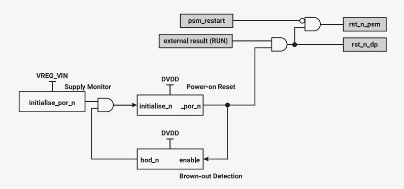
The diagram illustrates the chip-level reset subsystem. It shows the following components and connections:
- VREG_VIN is connected to a Supply Monitor .
- The Supply Monitor output goes to an initialise_por_n block.
- DVDD is connected to the initialise_por_n block.
- The initialise_por_n block outputs to a Power-on Reset block.
- The Power-on Reset block outputs to an initialise_n_por_n block.
- The initialise_n_por_n block outputs to a bod_n block.
- The bod_n block has an enable input and is labeled Brown-out Detection .
- The psm_restart input and the output of the initialise_n_por_n block are connected to an AND gate.
- The output of this AND gate is connected to the rst_n_psm output.
- The output of the initialise_n_por_n block is also connected to another AND gate.
- The output of this second AND gate is connected to the rst_n_dp output.
2.12.2. Power-on Reset
The power-on reset block makes sure the chip starts up cleanly when power is first applied by holding it in reset until the digital core supply (DVDD) can reliably power the chip’s core logic. The block holds its
por_n
output low until DVDD has been above the
power-on reset threshold
(
\(
DVDD_{TH,POR}
\)
) for a period greater than the
power-on reset assertion delay
(
\(
t_{POR,ASSERT}
\)
). Once high,
por_n
remains high even if DVDD subsequently falls below
\(
DVDD_{TH,POR}
\)
, unless brown-out detection is enabled. The behaviour of
por_n
when power is applied is shown in
Figure 22
.
\(
DVDD_{TH,POR}
\)
is fixed at a nominal 0.957V, which should result in a threshold between 0.924V and 0.99V. The threshold assumes a nominal DVDD of 1.1V at initial power-on, and
por_n
may never go high if a lower voltage is used. Once the chip is out of reset, DVDD can be reduced without
por_n
going low, as long as brown-out detection has been disabled or a suitable threshold voltage has been set.
Figure 22. A power-on reset cycle
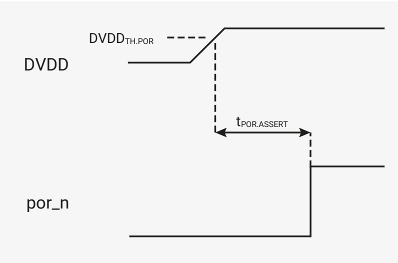
The timing diagram shows the relationship between DVDD and por_n during a power-on reset cycle:
- DVDD is shown as a signal that rises from a low level to a high level.
- por_n is shown as a signal that is initially low.
- A dashed horizontal line indicates the \( DVDD_{TH,POR} \) threshold.
- When DVDD rises above the threshold, por_n transitions from low to high.
- A horizontal double-headed arrow labeled \( t_{POR,ASSERT} \) indicates the time delay between DVDD crossing the threshold and por_n becoming high.
- After por_n becomes high, it remains high even if DVDD subsequently falls below the threshold.
2.12.2.1. Detailed Specifications
Table 193. Power-on Reset Parameters
| Parameter | Description | Min | Typ | Max | Units |
|---|---|---|---|---|---|
| DVDD TH.POR | power-on reset threshold | 0.924 | 0.957 | 0.99 | V |
| t POR.ASSERT | power-on reset assertion delay | 3 | 10 | µs |
2.12.3. Brown-out Detection
The brown-out detection block prevents unreliable operation by initiating a power-on reset cycle if the digital core supply (DVDD) drops below a safe operating level. The block's
bod_n
output is taken low if DVDD drops below the
brown-out detection threshold
(DVDD
TH.BOD
) for a period longer than the
brown-out detection assertion delay
(t
BOD.ASSERT
). This re-initialises the power-on reset block, which resets the chip, by taking its
por_n
output low, and holds it in reset until DVDD returns to a safe operating level. Figure 23 shows a brown-out event and the subsequent power-on reset cycle.
Figure 23. A brown-out detection cycle
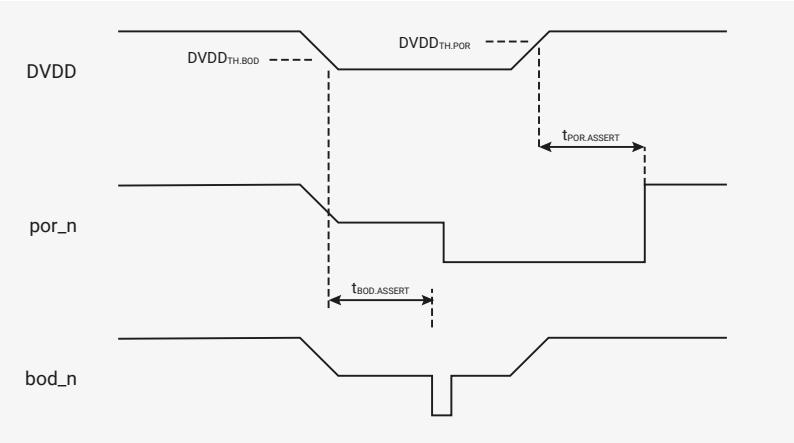
2.12.3.1. Detection Enable
Brown-out detection is automatically enabled at initial power-on or after a brown-out initiated reset. There is, however, a short delay, the
brown-out detection activation delay
(t
BOD.ACTIVE
), between
por_n
going high and detection becoming active. This is shown in Figure 24.
Figure 24. Activation of brown-out detection at initial power-on and following a brown-out event.
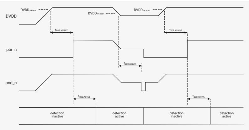
Once the chip is out of reset, detection can be disabled under software control. This also saves a small amount of power. If detection is subsequently re-enabled, there will be another short delay, the brown-out detection enable delay (t BOD.ENABLE ), before it becomes active again. This is shown in Figure 25.
Detection is disabled by writing a zero to the EN field in the BOD register and is re-enabled by writing a one to the same field. The block's bod_n output is high when detection is disabled.
Figure 25. Disabling and enabling brown-out detection
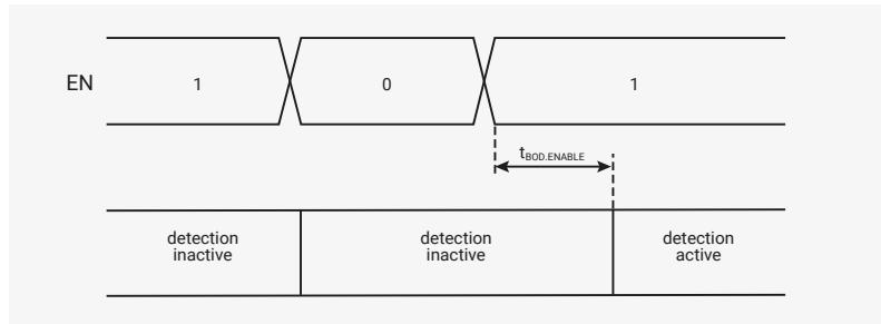
The diagram shows a signal trace for the EN field of the BOD register. The signal starts at 1, transitions to 0, and then transitions back to 1. Below the signal trace, the detection state is indicated: 'detection inactive' when EN is 0, and 'detection active' when EN is 1. A horizontal arrow labeled \( t_{BOD.ENABLE} \) indicates the delay between the EN signal transitioning from 0 to 1 and the detection becoming active.
Detection is re-enabled if the BOD register is reset, as this sets the register's EN field to one. Again, detection will become active after a delay equal to the brown-out detection enable delay ( \( t_{BOD.ENABLE} \) ).
NOTE
If the BOD register is reset by a power-on or brown-out initiated reset, the delay between the register being reset and brown-out detection becoming active will be equal to the brown-out detection activation delay ( \( t_{BOD.ACTIVE} \) ). The delay will be equal to the brown-out detection enable delay ( \( t_{BOD.ENABLE} \) ) for all other reset sources.
2.12.3.2. Adjusting the Detection Threshold
The brown-out detection threshold ( \( DVDD_{TH.BOD} \) ) has a nominal value of 0.86V at initial power-on or after a reset event. This should result in a detection threshold between 0.83V and 0.89V. Once out of reset, the threshold can be adjusted under software control. The new detection threshold will take effect after the brown-out detection programming delay ( \( t_{BOD.PROG} \) ). An example of this is shown in Figure 26 .
The threshold is adjusted by writing to the VSEL field in the BOD register. See the BOD register description for details.
Figure 26. Adjusting the brown-out detection threshold
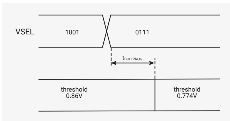
The diagram shows a signal trace for the VSEL field of the BOD register. The signal starts at 1001, transitions to 0111, and then transitions back to 1001. Below the signal trace, the detection threshold is indicated: 'threshold 0.86V' when VSEL is 1001, and 'threshold 0.774V' when VSEL is 0111. A horizontal arrow labeled \( t_{BOD.PROG} \) indicates the delay between the VSEL signal transitioning from 1001 to 0111 and the threshold becoming 0.774V.
2.12.3.3. Detailed Specifications
Table 194. Brown-out Detection Parameters
| Parameter | Description | Min | Typ | Max | Units |
|---|---|---|---|---|---|
| \( DVDD_{TH.BOD} \) | brown-out detection threshold | 96.5 | 100 | 103.5 | % of selected threshold voltage |
| \( t_{BOD.ACTIVE} \) | brown-out detection activation delay | 55 | 80 | \( \mu s \) |
| Parameter | Description | Min | Typ | Max | Units |
|---|---|---|---|---|---|
| \( t_{\text{BOD,ASSERT}} \) | brown-out detection assertion delay | 3 | 10 | \( \mu\text{s} \) | |
| \( t_{\text{BOD,ENABLE}} \) | brown-out detection enable delay | 35 | 55 | \( \mu\text{s} \) | |
| \( t_{\text{BOD,PROG}} \) | brown-out detection programming delay | 20 | 30 | \( \mu\text{s} \) |
2.12.4. Supply Monitor
The power-on and brown-out reset blocks are powered by the on-chip voltage regulator's input supply (VREG_VIN). The blocks are initialised when power is first applied, but may not be reliably re-initialised if power is removed and then reapplied before VREG_VIN has dropped to a sufficiently low level. To prevent this happening, VREG_VIN is monitored and the power-on reset block is re-initialised if it drops below the VREG_VIN activation threshold (VREG_VIN TH,ACTIVE ). VREG_VIN TH,ACTIVE is fixed at a nominal 1.1V, which should result in a threshold between 0.87V and 1.26V. This threshold does not represent a safe operating voltage. It is the voltage that VREG_VIN must drop below to reliably re-initialise the power-on reset block. For safe operation, VREG_VIN must be at a nominal voltage between 1.8V and 3.3V.
2.12.4.1. Detailed Specifications
Table 195. Voltage Regulator Input Supply Monitor Parameters
| Parameter | Description | Min | Typ | Max | Units |
|---|---|---|---|---|---|
| VREG_VIN TH,ACTIVE | VREG_VIN activation threshold | 0.87 | 1.1 | 1.26 | V |
2.12.5. External Reset
The chip can also be reset by taking its RUN pin low. Taking RUN low will hold the chip in reset irrespective of the state of the core power supply (DVDD) and the power-on reset / brown-out detection blocks. The chip will come out of reset as soon as RUN is taken high, if all other reset sources have been released. RUN can be used to extend the initial power-on reset, or can be driven from an external source to start and stop the chip as required. If RUN is not used, it should be tied high.
2.12.6. Rescue Debug Port Reset
The chip can also be reset via the Rescue Debug Port. This allows the chip to be recovered from a locked up state. In addition to resetting the chip, a Rescue Debug Port reset also sets the
PSM_RESTART_FLAG
in the
CHIP_RESET
register. This is checked by the bootcode at startup, causing it to enter a safe state if the bit is set. See
Section 2.3.4.2, "Rescue DP"
for more information.
2.12.7. Source of Last Reset
The source of the most recent chip-level reset can be determined by reading the state of the
HAD_POR
,
HAD_RUN
and
HAD_PSM_RESTART
fields in the
CHIP_RESET
register. A one in the
HAD_POR
field indicates a power supply related reset, i.e. either a power-on or brown-out initiated reset, a one in the
HAD_RUN
field indicates the chip was last reset by the RUN pin, and a one in the
HAD_PSM_RESTART
field indicates the chip has been reset via Rescue Debug Port. There should never be more than one field set to one.
2.12.8. List of Registers
The chip-level reset subsystem shares a register address space with the on-chip voltage regulator. The registers for both subsystems are listed in
Section 2.10.6
. The shared address space is referred to as
vreg_and_chip_reset
elsewhere in this document.
2.13. Power-On State Machine
2.13.1. Overview
The power-on state machine removes the reset from various hardware blocks in a specific order. Each peripheral in the power-on state machine is controlled by an internal
rst_n
active-low reset signal and generates an internal
rst_done
active-high reset done signal. The power-on state machine deasserts the reset to each peripheral, waits for that peripheral to assert its
rst_done
and then deasserts the reset to the next peripheral. An important use of this is to wait for a clock source to be running cleanly in the chip before the reset to the clock generators is deasserted. This avoids potentially glitchy clocks being distributed to the chip.
The power-on state machine is itself taken out of reset when the Chip-Level Reset subsystem confirms that the digital core supply (DVDD) is powered and stable, and the
RUN
pin is high. The power-on state machine takes a number of other blocks out of reset at this point via its
rst_n_run
output. This is used to reset things that need to be reset at start-up but must not be reset if the power-on state machine is restarted. This list includes:
- • Power on logic in the ring oscillator and crystal oscillator
- • Clock dividers which must keep on running during a power-on state machine restart (
clk_refandclk_sys) - • Watchdog (contains scratch registers which need to persist through a soft-restart of the power-on state machine)
2.13.2. Power On Sequence
Figure 27. Power-On State Machine Sequence.
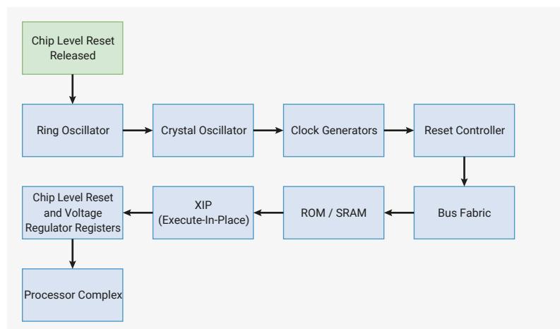
graph TD
    A[Chip Level Reset Released] --> B[Ring Oscillator]
    B --> C[Crystal Oscillator]
    C --> D[Clock Generators]
    D --> E[Reset Controller]
    E --> F[Bus Fabric]
    F --> G[ROM / SRAM]
    G --> H[XIP (Execute-In-Place)]
    H --> I[Chip Level Reset and Voltage Regulator Registers]
    I --> J[Processor Complex]
The power-on state machine sequence is as follows:
- • Chip-Level Reset subsystem deasserts power-on state machine reset once digital core supply (DVDD) is powered and stable, and RUN pin is high ( rst_n_run is also deasserted at this point)
- • Ring Oscillator is started. rst_done is asserted once the ripple counter has seen a sufficient number of clock edges to indicate the ring oscillator is stable
- • Crystal Oscillator reset is deasserted. The crystal oscillator is not started at this point, so rst_done is asserted instantly.
- • clk_ref and clk_sys clock generators are taken out of reset. In the initial configuration clk_ref is running from the ring oscillator with no divider. clk_sys is running from clk_ref . These clocks are needed for the rest of the sequence to progress.
The rest of the sequence is fairly simple, with the following coming out of reset in order one by one:
- • Reset Controller - used to reset all non-boot peripherals
- • Chip-Level Reset and Voltage Regulator registers - used by the bootrom to check the boot state of the chip. In particular, the PSM_RESTART_FLAG flag in the CHIP_RESET register can be set via SWD to indicate to the boot code that there is bad code in flash and it should stop executing. The reset state of the CHIP_RESET register is determined by the Chip-Level Reset subsystem and is not affected by reset coming from the power-on state machine
- • XIP (Execute-In-Place) - used by the bootrom to execute code from an external SPI flash
- • ROM and SRAM - Boot code is executed from the ROM. SRAM is used by processors and Bus Fabric.
- • Bus Fabric - Allows the processors to communicate with peripherals
- • Processor complex - Finally the processors can start running
The final thing to come out of reset is the processor complex. This includes both core0 and core1 . Both cores will start executing the bootcode from ROM. One of the first things the bootrom does is read the core id. At this point, core1 will go to sleep leaving core0 to continue with the bootrom execution. The processor complex has its own reset control and various low-power modes which is why both the core0 and core1 resets are deasserted, despite only core0 being needed for the bootrom.
2.13.3. Register Control
The power-on state machine is a fully automated piece of hardware. It requires no input from the user to work. There are register controls that can be used to override and see the status of the power-on state machine. This allows hardware blocks in the power-on state machine to be reset by software if necessary. There is also a WDSSEL register which is used to control what is reset by a Watchdog reset.
2.13.4. Interaction with Watchdog
The power-on state machine can be restarted from a software-programmable position if the Watchdog fires. For example, in the case the processor is stuck in an infinite loop, or the programmer has somehow misconfigured the chip. It is important to note that if a peripheral in the power-on state machine has the WDSSEL bit set, every peripheral after it in the power-on sequence will also be reset because the rst_done of the selected peripheral will be deasserted, asserting rst_n for the remaining peripherals.
2.13.5. List of Registers
The PSM registers start at a base address of 0x40010000 (defined as PSM_BASE in SDK).
Table 196. List of PSM registers
| Offset | Name | Info |
|---|---|---|
| 0x0 | FRCE_ON | Force block out of reset (i.e. power it on) |
| 0x4 | FRCE_OFF | Force into reset (i.e. power it off) |
| 0x8 | WDSEL | Set to 1 if this peripheral should be reset when the watchdog fires. |
| 0xc | DONE | Indicates the peripheral's registers are ready to access. |
PSM: FRCE_ON Register
Offset: 0x0
Description
Force block out of reset (i.e. power it on)
Table 197. FRCE_ON Register
| Bits | Description | Type | Reset |
|---|---|---|---|
| 31:17 | Reserved. | - | - |
| 16 | PROC1 | RW | 0x0 |
| 15 | PROC0 | RW | 0x0 |
| 14 | SIO | RW | 0x0 |
| 13 | VREG_AND_CHIP_RESET | RW | 0x0 |
| 12 | XIP | RW | 0x0 |
| 11 | SRAM5 | RW | 0x0 |
| 10 | SRAM4 | RW | 0x0 |
| 9 | SRAM3 | RW | 0x0 |
| 8 | SRAM2 | RW | 0x0 |
| 7 | SRAM1 | RW | 0x0 |
| 6 | SRAM0 | RW | 0x0 |
| 5 | ROM | RW | 0x0 |
| 4 | BUSFABRIC | RW | 0x0 |
| 3 | RESETS | RW | 0x0 |
| 2 | CLOCKS | RW | 0x0 |
| 1 | XOSC | RW | 0x0 |
| 0 | ROSC | RW | 0x0 |
PSM: FRCE_OFF Register
Offset: 0x4
Description
Force into reset (i.e. power it off)
Table 198. FRCE_OFF Register
| Bits | Description | Type | Reset |
|---|---|---|---|
| 31:17 | Reserved. | - | - |
| 16 | PROC1 | RW | 0x0 |
| Bits | Description | Type | Reset |
|---|---|---|---|
| 15 | PROC0 | RW | 0x0 |
| 14 | SIO | RW | 0x0 |
| 13 | VREG_AND_CHIP_RESET | RW | 0x0 |
| 12 | XIP | RW | 0x0 |
| 11 | SRAM5 | RW | 0x0 |
| 10 | SRAM4 | RW | 0x0 |
| 9 | SRAM3 | RW | 0x0 |
| 8 | SRAM2 | RW | 0x0 |
| 7 | SRAM1 | RW | 0x0 |
| 6 | SRAM0 | RW | 0x0 |
| 5 | ROM | RW | 0x0 |
| 4 | BUSFABRIC | RW | 0x0 |
| 3 | RESETS | RW | 0x0 |
| 2 | CLOCKS | RW | 0x0 |
| 1 | XOSC | RW | 0x0 |
| 0 | ROSC | RW | 0x0 |
PSM: WDSSEL Register
Offset: 0x8
Description
Set to 1 if this peripheral should be reset when the watchdog fires.
Table 199. WDSSEL Register
| Bits | Description | Type | Reset |
|---|---|---|---|
| 31:17 | Reserved. | - | - |
| 16 | PROC1 | RW | 0x0 |
| 15 | PROC0 | RW | 0x0 |
| 14 | SIO | RW | 0x0 |
| 13 | VREG_AND_CHIP_RESET | RW | 0x0 |
| 12 | XIP | RW | 0x0 |
| 11 | SRAM5 | RW | 0x0 |
| 10 | SRAM4 | RW | 0x0 |
| 9 | SRAM3 | RW | 0x0 |
| 8 | SRAM2 | RW | 0x0 |
| 7 | SRAM1 | RW | 0x0 |
| 6 | SRAM0 | RW | 0x0 |
| 5 | ROM | RW | 0x0 |
| 4 | BUSFABRIC | RW | 0x0 |
| Bits | Description | Type | Reset |
|---|---|---|---|
| 3 | RESETS | RW | 0x0 |
| 2 | CLOCKS | RW | 0x0 |
| 1 | XOSC | RW | 0x0 |
| 0 | ROSC | RW | 0x0 |
PSM: DONE Register
Offset: 0xc
Description
Indicates the peripheral's registers are ready to access.
Table 200. DONE Register
| Bits | Description | Type | Reset |
|---|---|---|---|
| 31:17 | Reserved. | - | - |
| 16 | PROC1 | RO | 0x0 |
| 15 | PROC0 | RO | 0x0 |
| 14 | SIO | RO | 0x0 |
| 13 | VREG_AND_CHIP_RESET | RO | 0x0 |
| 12 | XIP | RO | 0x0 |
| 11 | SRAM5 | RO | 0x0 |
| 10 | SRAM4 | RO | 0x0 |
| 9 | SRAM3 | RO | 0x0 |
| 8 | SRAM2 | RO | 0x0 |
| 7 | SRAM1 | RO | 0x0 |
| 6 | SRAM0 | RO | 0x0 |
| 5 | ROM | RO | 0x0 |
| 4 | BUSFABRIC | RO | 0x0 |
| 3 | RESETS | RO | 0x0 |
| 2 | CLOCKS | RO | 0x0 |
| 1 | XOSC | RO | 0x0 |
| 0 | ROSC | RO | 0x0 |
2.14. Subsystem Resets
2.14.1. Overview
The reset controller allows software control of the resets to all of the peripherals that are not critical to boot the processor in RP2040. This includes:
- • USB Controller
- • PIO
- • Peripherals such as UART, I2C, SPI, PWM, Timer, ADC
- • PLLs
- • IO and Pad registers
The full list can be seen in the register descriptions.
Every peripheral reset by the reset controller is held in reset at power-up. It is up to software to deassert the reset of peripherals it intends to use. Note that if you are using the SDK some peripherals may already be out of reset.
2.14.2. Programmer's Model
The SDK defines a struct to represent the resets registers.
SDK: https://github.com/raspberrypi/pico-sdk/blob/master/src/rp2040/hardware_structs/include/hardware/structs/resets.h Lines 59 - 146
59 typedef struct {
60     _REG_(RESETS_RESET_OFFSET) // RESETS_RESET
61     // Reset control.
62     // 0x01000000 [24] USBCTRL      (1)
63     // 0x00800000 [23] UART1       (1)
64     // 0x00400000 [22] UART0       (1)
65     // 0x00200000 [21] TIMER       (1)
66     // 0x00100000 [20] TBMAN        (1)
67     // 0x00080000 [19] SYSINFO      (1)
68     // 0x00040000 [18] SYSCFG       (1)
69     // 0x00020000 [17] SPI1         (1)
70     // 0x00010000 [16] SPI0         (1)
71     // 0x00008000 [15] RTC          (1)
72     // 0x00004000 [14] PWM          (1)
73     // 0x00002000 [13] PLL_USB      (1)
74     // 0x00001000 [12] PLL_SYS      (1)
75     // 0x00000800 [11] PIO1         (1)
76     // 0x00000400 [10] PIO0         (1)
77     // 0x00000200 [9] PADS_QSPI     (1)
78     // 0x00000100 [8] PADS_BANK0    (1)
79     // 0x00000080 [7] JTAG          (1)
80     // 0x00000040 [6] IO_QSPI       (1)
81     // 0x00000020 [5] IO_BANK0      (1)
82     // 0x00000010 [4] I2C1          (1)
83     // 0x00000008 [3] I2C0          (1)
84     // 0x00000004 [2] DMA           (1)
85     // 0x00000002 [1] BUSCTRL       (1)
86     // 0x00000001 [0] ADC           (1)
87     io_rw_32 reset;
88
89     _REG_(RESETS_WDSEL_OFFSET) // RESETS_WDSEL
90     // Watchdog select.
91     // 0x01000000 [24] USBCTRL      (0)
92     // 0x00800000 [23] UART1       (0)
93     // 0x00400000 [22] UART0       (0)
94     // 0x00200000 [21] TIMER       (0)
95     // 0x00100000 [20] TBMAN        (0)
96     // 0x00080000 [19] SYSINFO      (0)
97     // 0x00040000 [18] SYSCFG       (0)
98     // 0x00020000 [17] SPI1         (0)
99     // 0x00010000 [16] SPI0         (0)
100    // 0x00008000 [15] RTC          (0)
101    // 0x00004000 [14] PWM          (0)
102    // 0x00002000 [13] PLL_USB      (0)
103 // 0x00001000 [12] PLL_SYS (0)
104 // 0x00000800 [11] PIO1 (0)
105 // 0x00000400 [10] PIO0 (0)
106 // 0x00000200 [9] PADS_QSPI (0)
107 // 0x00000100 [8] PADS_BANK0 (0)
108 // 0x00000080 [7] JTAG (0)
109 // 0x00000040 [6] IO_QSPI (0)
110 // 0x00000020 [5] IO_BANK0 (0)
111 // 0x00000010 [4] I2C1 (0)
112 // 0x00000008 [3] I2C0 (0)
113 // 0x00000004 [2] DMA (0)
114 // 0x00000002 [1] BUSCTRL (0)
115 // 0x00000001 [0] ADC (0)
116 io_rw_32 wdsel;
117
118 _REG(RESETS_RESET_DONE_OFFSET) // RESETS_RESET_DONE
119 // Reset done.
120 // 0x01000000 [24] USBCTRL (0)
121 // 0x00800000 [23] UART1 (0)
122 // 0x00400000 [22] UART0 (0)
123 // 0x00200000 [21] TIMER (0)
124 // 0x00100000 [20] TBMAN (0)
125 // 0x00080000 [19] SYSINFO (0)
126 // 0x00040000 [18] SYSCFG (0)
127 // 0x00020000 [17] SPI1 (0)
128 // 0x00010000 [16] SPI0 (0)
129 // 0x00008000 [15] RTC (0)
130 // 0x00004000 [14] PWM (0)
131 // 0x00002000 [13] PLL_USB (0)
132 // 0x00001000 [12] PLL_SYS (0)
133 // 0x00000800 [11] PIO1 (0)
134 // 0x00000400 [10] PIO0 (0)
135 // 0x00000200 [9] PADS_QSPI (0)
136 // 0x00000100 [8] PADS_BANK0 (0)
137 // 0x00000080 [7] JTAG (0)
138 // 0x00000040 [6] IO_QSPI (0)
139 // 0x00000020 [5] IO_BANK0 (0)
140 // 0x00000010 [4] I2C1 (0)
141 // 0x00000008 [3] I2C0 (0)
142 // 0x00000004 [2] DMA (0)
143 // 0x00000002 [1] BUSCTRL (0)
144 // 0x00000001 [0] ADC (0)
145 io_ro_32 reset_done;
146 } resets_hw_t;
Three registers are defined:
- • reset : this register contains a bit for each peripheral that can be reset. If the bit is set to 1 then the reset is asserted. If the bit is cleared then the reset is deasserted.
- • wdsel : if the bit is set then this peripheral will be reset if the watchdog fires (note that the power on state machine can potentially reset the whole reset controller, which will reset everything)
- • reset_done : a bit for each peripheral, that gets set once the peripheral is out of reset. This allows software to wait for this status bit in case the peripheral has some initialisation to do before it can be used.
The reset functions in the SDK are defined as follows:
SDK: https://github.com/raspberrypi/pico-sdk/blob/master/src/rp2-common/hardware_resets/include/hardware/resets.h Lines 121 - 123
121 static __force_inline void reset_block(uint32_t bits) {
122     reset_block_mask(bits);
123 }
SDK: https://github.com/raspberrypi/pico-sdk/blob/master/src/rp2_common/hardware_resets/include/hardware/resets.h Lines 125 - 127
125 static __force_inline void unreset_block(uint32_t bits) {
126     unreset_block_mask(bits);
127 }
SDK: https://github.com/raspberrypi/pico-sdk/blob/master/src/rp2_common/hardware_resets/include/hardware/resets.h Lines 129 - 131
129 static __force_inline void unreset_block_wait(uint32_t bits) {
130     return unreset_block_mask_wait_blocking(bits);
131 }
An example use of these is in the UART driver, where the driver defines a
uart_reset
function, selecting a different bit of the reset register depending on the uart specified:
SDK: https://github.com/raspberrypi/pico-sdk/blob/master/src/rp2_common/hardware_uart/uart.c Lines 32 - 38
32 static inline void uart_reset(uart_inst_t *uart) {
33     reset_block_num(uart_get_reset_num(uart));
34 }
35
36 static inline void uart_unreset(uart_inst_t *uart) {
37     unreset_block_num_wait_blocking(uart_get_reset_num(uart));
38 }
2.14.3. List of Registers
The reset controller registers start at a base address of
0x4000c000
(defined as
RESETS_BASE
in SDK).
Table 201. List of RESETS registers
| Offset | Name | Info |
|---|---|---|
| 0x0 | RESET | Reset control. |
| 0x4 | WDSEL | Watchdog select. |
| 0x8 | RESET_DONE | Reset done. |
RESETS: RESET Register
Offset: 0x0
Description
Reset control. If a bit is set it means the peripheral is in reset. 0 means the peripheral's reset is deasserted.
Table 202. RESET Register
| Bits | Description | Type | Reset |
|---|---|---|---|
| 31:25 | Reserved. | - | - |
| 24 | USBCTRL | RW | 0x1 |
| 23 | UART1 | RW | 0x1 |
| 22 | UART0 | RW | 0x1 |
| 21 | TIMER | RW | 0x1 |
| Bits | Description | Type | Reset |
|---|---|---|---|
| 20 | TBMAN | RW | 0x1 |
| 19 | SYSINFO | RW | 0x1 |
| 18 | SYSCFG | RW | 0x1 |
| 17 | SPI1 | RW | 0x1 |
| 16 | SPI0 | RW | 0x1 |
| 15 | RTC | RW | 0x1 |
| 14 | PWM | RW | 0x1 |
| 13 | PLL_USB | RW | 0x1 |
| 12 | PLL_SYS | RW | 0x1 |
| 11 | PIO1 | RW | 0x1 |
| 10 | PIO0 | RW | 0x1 |
| 9 | PADS_QSPI | RW | 0x1 |
| 8 | PADS_BANK0 | RW | 0x1 |
| 7 | JTAG | RW | 0x1 |
| 6 | IO_QSPI | RW | 0x1 |
| 5 | IO_BANK0 | RW | 0x1 |
| 4 | I2C1 | RW | 0x1 |
| 3 | I2C0 | RW | 0x1 |
| 2 | DMA | RW | 0x1 |
| 1 | BUSCTRL | RW | 0x1 |
| 0 | ADC | RW | 0x1 |
RESETS: WDSSEL Register
Offset: 0x4
Description
Watchdog select. If a bit is set then the watchdog will reset this peripheral when the watchdog fires.
Table 203. WDSSEL Register
| Bits | Description | Type | Reset |
|---|---|---|---|
| 31:25 | Reserved. | - | - |
| 24 | USBCTRL | RW | 0x0 |
| 23 | UART1 | RW | 0x0 |
| 22 | UART0 | RW | 0x0 |
| 21 | TIMER | RW | 0x0 |
| 20 | TBMAN | RW | 0x0 |
| 19 | SYSINFO | RW | 0x0 |
| 18 | SYSCFG | RW | 0x0 |
| 17 | SPI1 | RW | 0x0 |
| Bits | Description | Type | Reset |
|---|---|---|---|
| 16 | SPI0 | RW | 0x0 |
| 15 | RTC | RW | 0x0 |
| 14 | PWM | RW | 0x0 |
| 13 | PLL_USB | RW | 0x0 |
| 12 | PLL_SYS | RW | 0x0 |
| 11 | PIO1 | RW | 0x0 |
| 10 | PIO0 | RW | 0x0 |
| 9 | PADS_QSPI | RW | 0x0 |
| 8 | PADS_BANK0 | RW | 0x0 |
| 7 | JTAG | RW | 0x0 |
| 6 | IO_QSPI | RW | 0x0 |
| 5 | IO_BANK0 | RW | 0x0 |
| 4 | I2C1 | RW | 0x0 |
| 3 | I2C0 | RW | 0x0 |
| 2 | DMA | RW | 0x0 |
| 1 | BUSCTRL | RW | 0x0 |
| 0 | ADC | RW | 0x0 |
RESETS: RESET_DONE Register
Offset: 0x8
Description
Reset done. If a bit is set then a reset done signal has been returned by the peripheral. This indicates that the peripheral's registers are ready to be accessed.
Table 204.
RESET_DONE Register
| Bits | Description | Type | Reset |
|---|---|---|---|
| 31:25 | Reserved. | - | - |
| 24 | USBCTRL | RO | 0x0 |
| 23 | UART1 | RO | 0x0 |
| 22 | UART0 | RO | 0x0 |
| 21 | TIMER | RO | 0x0 |
| 20 | TBMAN | RO | 0x0 |
| 19 | SYSINFO | RO | 0x0 |
| 18 | SYSCFG | RO | 0x0 |
| 17 | SPI1 | RO | 0x0 |
| 16 | SPI0 | RO | 0x0 |
| 15 | RTC | RO | 0x0 |
| 14 | PWM | RO | 0x0 |
| 13 | PLL_USB | RO | 0x0 |
| Bits | Description | Type | Reset |
|---|---|---|---|
| 12 | PLL_SYS | RO | 0x0 |
| 11 | PIO1 | RO | 0x0 |
| 10 | PIO0 | RO | 0x0 |
| 9 | PADS_QSPI | RO | 0x0 |
| 8 | PADS_BANK0 | RO | 0x0 |
| 7 | JTAG | RO | 0x0 |
| 6 | IO_QSPI | RO | 0x0 |
| 5 | IO_BANK0 | RO | 0x0 |
| 4 | I2C1 | RO | 0x0 |
| 3 | I2C0 | RO | 0x0 |
| 2 | DMA | RO | 0x0 |
| 1 | BUSCTRL | RO | 0x0 |
| 0 | ADC | RO | 0x0 |
2.15. Clocks
2.15.1. Overview
The clocks block provides independent clocks to on-chip and external components. It takes inputs from a variety of clock sources allowing the user to trade off performance against cost, board area and power consumption. From these sources it uses multiple clock generators to provide the required clocks. This architecture allows the user flexibility to start and stop clocks independently and to vary some clock frequencies whilst maintaining others at their optimum frequencies.
Figure 28. Clocks overview
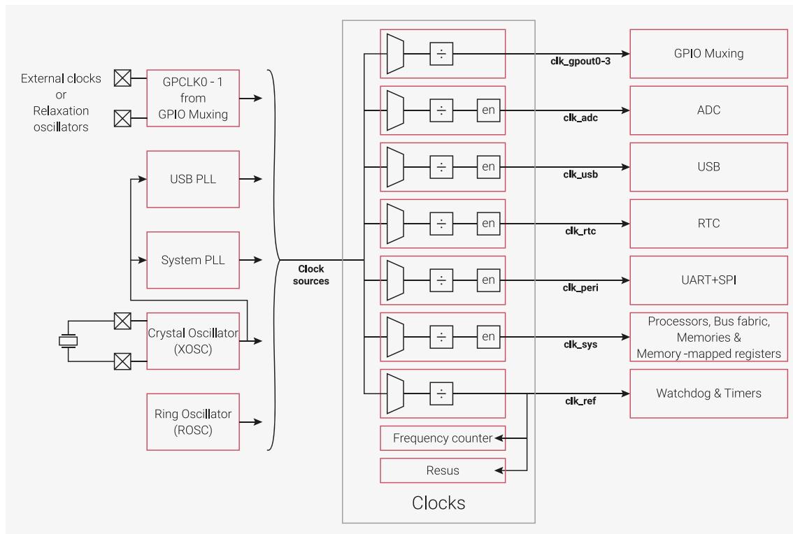
For very low cost or low power applications where precise timing is not required, the chip can be run from the internal Ring Oscillator (ROSC). Alternatively the user can provide external clocks or construct simple relaxation oscillators using the GPIOs and appropriate external passive components. Where timing is more critical, the Crystal Oscillator (XOSC) can provide an accurate reference to the 2 on-chip PLLs to provide fast clocking at precise frequencies.
The clock generators select from the clock sources and optionally divide the selected clock before outputting through enable logic which provides automatic clock disabling in SLEEP mode (see Section 2.11.2 ).
An on-chip frequency counter facilitates debugging of the clock setup and also allows measurement of the frequencies of external clocks. The on-chip resus component restarts the system clock from a known good clock if it is accidentally stopped. This allows the software debugger to access registers and debug the problem.
The chip has an ultra-low power mode called DORMANT (see Section 2.11.3 ) in which all on-chip clock sources are stopped to save power. External sources are not stopped and can be used to provide a clock to the on-chip RTC which can provide an alarm to wake the chip from DORMANT mode. Alternatively the GPIO interrupts can be configured to wake the chip from DORMANT mode in response to an external event.
Up to 4 generated clocks can be output to GPIOs at up to 50MHz. This allows the user to supply clocks to external devices, thus reducing component counts in power, space and cost sensitive applications.
2.15.2. Clock sources
The RP2040 can be run from a variety of clock sources. This flexibility allows the user to optimise the clock setup for performance, cost, board area and power consumption. The sources include the on-chip Ring Oscillator ( Section 2.17 ), the Crystal Oscillator ( Section 2.16 ), external clocks from GPIOs ( Section 2.15.6.4 ) and the PLLs ( Section 2.18 ).
The list of clock sources is different per clock generator and can be found as enumerated values in the CTRL register. See
CLK_SYS_CTRL
as an example.
2.15.2.1. Ring Oscillator
The on-chip Ring Oscillator ( Section 2.17 ) requires no external components. It runs automatically from power-up and is used to clock the chip during the initial boot stages. The startup frequency is typically 6MHz but varies with PVT (Process, Voltage and Temperature). The frequency is likely to be in the range 4-8MHz and is guaranteed to be in the range 1.8-12MHz.
For low cost applications where frequency accuracy is unimportant, the chip can continue to run from the ROSC. If greater performance is required the frequency can be increased by programming the registers as described in Section 2.17 . The frequency will vary with PVT (Process, Voltage and Temperature) so the user must take care to avoid exceeding the maximum frequencies described in the clock generators section. This variation can be mitigated in various ways (see Section 2.15.2.1.1 ) if the user wants to continue running from the ROSC at a frequency close to the maximum. Alternatively, the user can use an external clock or the XOSC to provide a stable reference clock and use the PLLs to generate higher frequencies. This will require external components, which will cost board area and increase power consumption.
If an external clock or the XOSC is used then the ROSC can be stopped to save power. However, the reference clock generator and the system clock generator must be switched to an alternate source before doing so.
The ROSC is not affected by SLEEP mode. If required the frequency can be reduced before entering SLEEP mode to save power. On entering DORMANT mode the ROSC is automatically stopped and is restarted in the same configuration when exiting DORMANT mode. If the ROSC is driving clocks at close to their maximum frequencies then it is recommended to drop the frequency before entering SLEEP or DORMANT mode to allow for frequency variation due to changes in environmental conditions during SLEEP or DORMANT mode.
If the user wants to use the ROSC clock externally then it can be output to a GPIO pin using one of the clk_gpclk0-3 generators.
The following sections describe techniques for mitigating PVT variation of the ROSC frequency. They also provide some interesting design challenges for use in teaching both the effects of PVT and writing software to control real time functions.
 NOTE
NOTE
The ROSC frequency varies with PVT so the user can send its output to the frequency counter and use it to measure any 1 of these 3 variables if the other 2 are known.
2.15.2.1.1. Mitigating ROSC frequency variation due to process
Process varies for two reasons. Firstly, chips leave the factory with a spread of process parameters which cause variation in the ROSC frequency across chips. Secondly, process parameters vary slightly as the chip ages, though this will only be observable over many thousands of hours of operation. To mitigate for process variation, the user can characterise individual chips and program the ROSC frequency accordingly. This is an adequate solution for small numbers of chips but is not suitable for volume production. In such applications the user should consider using the automatic mitigation techniques described below.
2.15.2.1.2. Mitigating ROSC frequency variation due to voltage
Supply voltage varies for two reasons. Firstly, the power supply itself may vary, and secondly, there will be varying on-chip IR drop as chip activity varies. If the application has a minimum performance target then the user needs to calibrate for that application and adjust the ROSC frequency to ensure it always exceeds the minimum required.
2.15.2.1.3. Mitigating ROSC frequency variation due to temperature
Temperature varies for two reasons. Firstly, the ambient temperature may vary, and secondly, the chip temperature will vary as chip activity varies due to self-heating. This can be mitigated by stabilising the temperature using a temperature
controlled environment and passive or active cooling. Alternatively the user can track the temperature using the on-chip temperature sensor and adjust the ROSC frequency so it remains within the required bounds.
2.15.2.1.4. Automatic mitigation of ROSC frequency variation due to PVT
Techniques for automatic ROSC frequency control avoid the need to calibrate individual chips but require periodic access to a clock reference or to a time reference. If a clock reference is available then it can be used to periodically measure the ROSC frequency and adjust it accordingly. The reference could be the on-chip XOSC which can be turned on periodically for this purpose. This may be useful in a very low power application where it is too costly to run the XOSC continuously and too costly to use the PLLs to achieve high frequencies. If a time reference is available then the user could clock the on-chip RTC from the ROSC and periodically compare it against the time reference, then adjust the ROSC frequency as necessary. Using these techniques the ROSC frequency will drift due to VT variation so the user must take care that these variations do not allow the ROSC frequency to drift out of the acceptable range.
2.15.2.1.5. Automatic overclocking using the ROSC
The datasheet maximum frequencies for any digital device are quoted for worst case PVT. Most chips in most normal environments can run significantly faster than the quoted maximum and can therefore be overclocked. If the RP2040 is running from the ROSC then both the ROSC and the digital components are similarly affected by PVT, so, as the ROSC gets faster, the processors can also run faster. This means the user can overclock from the ROSC then rely on the ROSC frequency tracking with PVT variations. The tracking of ROSC frequency and the processor capability is not perfect and currently there is insufficient data to specify a safe ROSC setting for this mode of operation, so some experimentation is required.
This mode of operation will maximise processor performance but will lead to variations in the time taken to complete a task, which may be unacceptable in some applications. Also, if the user wants to use frequency sensitive interfaces such as USB or UART then the XOSC and PLL must be used to provide a precise clock for those components.
2.15.2.2. Crystal Oscillator
The Crystal Oscillator ( Section 2.16 ) provides a precise, stable clock reference and should be used where accurate timing is required and no suitable external clocks are available. The frequency is determined by the external crystal and the oscillator supports frequencies in the range 1MHz to 15MHz. The on-chip PLLs can be used to synthesise higher frequencies if required. The RP2040 reference design (see the Minimal Design Example in Hardware design with RP2040 ) uses a 12MHz crystal. Using the XOSC and the PLLs, the on-chip components can be run at their maximum frequencies. Appropriate margin is built into the design to tolerate up to 1000ppm variation in the XOSC frequency.
The XOSC is inactive on power up. If required it must be enabled in software. XOSC startup takes several milliseconds and the software must wait for the XOSC_STABLE flag to be set before starting the PLLs and before changing any clock generators to use it. Prior to that the output from the XOSC may be non-existent or may have very short pulse widths which will corrupt logic if used. Once it is running the reference clock (clk_ref) and the system clock (clk_sys) can be switched to run from the XOSC and the ROSC can be stopped to save power.
The XOSC is not affected by SLEEP mode. It is automatically stopped and restarted in the same configuration when entering and exiting DORMANT mode.
If the user wants to use the XOSC clock externally then it can be output to a GPIO pin using one of the clk_gpclk0-3 generators. It cannot be taken directly from the XIN or XOUT pins.
2.15.2.3. External Clocks
If external clocks exist in your hardware design then they can be used to clock the RP2040 either on their own or in conjunction with the XOSC or ROSC. This will potentially save power and will allow components on the RP2040 to be run synchronously with external components to simplify data transfer between chips. External clocks can be input on the
GPIN0 & GPIN1 GPIO inputs and on the XIN input to the XOSC. If the XIN input is used in this way the XOSC must be configured to pass through the XIN signal. All 3 inputs are limited to 50MHz but the on-chip PLLs can be used to synthesise higher frequencies from the XIN input if required. If the frequency accuracy of the external clocks is poorer than 1000ppm then the generated clocks should not be run at their maximum frequencies because they may exceed their design margins.
Once the external clocks are running, the reference clock (clk_ref) and the system clock (clk_sys) can be switched to run from the external clocks and the ROSC can be stopped to save power.
The external clock sources are not affected by SLEEP mode or DORMANT mode.
2.15.2.4. Relaxation Oscillators
If the user wants to use external clocks to replace or supplement the other clock sources but does not have an appropriate clock available, then 1 or 2 relaxation oscillators can be constructed using external passive components. Simply send the clock source (GPIN0 or GPIN1) to one of the gpclk0-3 generators, invert it through the GPIO inverter OUTOVER and connect back to the clock source input via an RC circuit.
Figure 29. Simple relaxation oscillator example
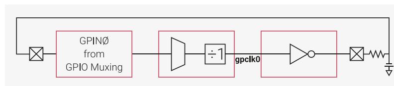
The frequency of clocks generated from relaxation oscillators will depend on the delay through the chip and the drive current from the GPIO output both of which vary with PVT. They will also depend on the quality and accuracy of the external components. It may be possible to improve the frequency accuracy using more elaborate external components such as ceramic resonators but that will increase cost and complexity and can never rival the XOSC. For that reason they are not discussed here. Given that these oscillators will not achieve 1000ppm then they cannot be used to drive internal clocks at their maximum frequencies.
The relaxation oscillators are not affected by SLEEP mode or DORMANT mode.
2.15.2.5. PLLs
The PLLs ( Section 2.18 ) are used to provide fast clocks when running from the XOSC (or an external clock source driven into the XIN pin). In a fully featured application the USB PLL provides a fixed 48MHz clock to the ADC and USB while clk_rtc and clk_ref are driven from the XOSC or external source. This allows the user to drive clk_sys from the system PLL and vary the frequency according to demand to save power without having to change the setups of the other clocks. clk_peri can be driven either from the fixed frequency USB PLL or from the variable frequency system PLL. If clk_sys never needs to exceed 48MHz then one PLL can be used and the divider in the clk_sys clock generator can be used to scale the clk_sys frequency according to demand.
When a PLL is started, its output cannot be used until the PLL locks as indicated by the LOCK bit in the STATUS register. Thereafter the PLL output cannot be used during changes to the reference clock divider, the output dividers or the bypass mode. The output can be used during feedback divisor changes with the proviso that the output frequency may overshoot or undershoot on large changes to the feedback divisor. For more information, see Section 2.18 .
If the PLL reference clock is accurate to 1000ppm then the PLLs can be used to drive clocks at their maximum frequency because the frequency of the generated clocks will be within the margins allowed in the design.
The PLLs are not affected by SLEEP mode. If the user wants to save power in SLEEP mode then all clock generators must be switched away from the PLLs and they must be stopped in software before entering SLEEP mode. The PLLs are not stopped and restarted automatically when entering and exiting DORMANT mode. If they are left running on entry to DORMANT mode they will be corrupted and will generate out of control clocks that will consume power unnecessarily. This happens because their reference clock from XOSC will be stopped. It is therefore essential to switch all clock generators away from the PLLs and stop the PLLs in software before entering DORMANT mode.
2.15.3. Clock Generators
The clock generators are built on a standard design which incorporates clock source multiplexing, division, duty cycle correction and SLEEP mode enabling. To save chip area and power, the individual clock generators do not support all features.
Figure 30. A generic clock generator
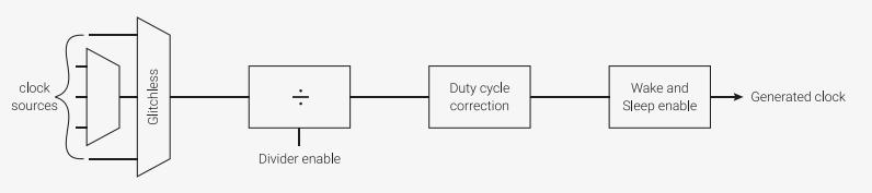
graph LR
    CS[clock sources] --> MUX[multiplexer]
    MUX --> G[Glitchless]
    G --> D[Divider]
    DE[Divider enable] --> D
    D --> DCC[Duty cycle correction]
    DCC --> WSE[Wake and Sleep enable]
WSE --> GC[Generated clock]2.15.3.1. Instances
RP2040 has several clock generators which are listed below.
Table 205. RP2040 clock generators
| Clock | Description | Nominal Frequency |
|---|---|---|
| clk_gpout0 | Clock output to GPIO. Can be used to clock external devices or debug on chip clocks with a logic analyser or oscilloscope. | N/A |
| clk_gpout1 | ||
| clk_gpout2 | ||
| clk_gpout3 | ||
| clk_ref | Reference clock that is always running unless in DORMANT mode. Runs from Ring Oscillator (ROSC) at power-up but can be switched to Crystal Oscillator (XOSC) for more accuracy. | 6 - 12MHz |
| clk_sys | System clock that is always running unless in DORMANT mode. Runs from clk_ref at power-up but is typically switched to a PLL. | 125MHz |
| clk_peri | Peripheral clock. Typically runs from clk_sys but allows peripherals to run at a consistent speed if clk_sys is changed by software. | 12 - 125MHz |
| clk_usb | USB reference clock. Must be 48MHz. | 48MHz |
| clk_adc | ADC reference clock. Must be 48MHz. | 48MHz |
| clk_rtc | RTC reference clock. The RTC divides this clock to generate a 1 second reference. | 46875Hz |
i NOTE
clk_sys (and clk_peri ) have a maximum frequency of 133MHz across all process, voltage and temperature variations. You can achieve 200MHz by running at an elevated core supply (DVDD) and setting VREG VSEL to 1.15V. For more information, see Section 2.10.6 .
For a full list of clock sources for each clock generator see the appropriate CTRL register. For example, CLK_SYS_CTRL .
2.15.3.2. Multiplexers
All clock generators have a multiplexer referred to as the auxiliary (aux) mux. This mux has a conventional design whose output will glitch when changing the select control. Two clock generators (
clk_sys
and
clk_ref
) have an additional multiplexer, referred to as the glitchless mux. The glitchless mux can switch between clock sources without generating a glitch on the output.
Clock glitches should be avoided at all costs because they may corrupt the logic running on that clock. This means that any clock generator with only an aux mux must be disabled while switching the clock source. If the clock generator has a glitchless mux (
clk_sys
and
clk_ref
), then the glitchless mux should switch away from the aux mux while changing the aux mux source. The clock generators require 2 cycles of the source clock to stop the output and 2 cycles of the new source to restart the output. The user must wait for the generator to stop before changing the auxiliary mux, and therefore must be aware of the source clock frequency.
The glitchless mux is only implemented for always-on clocks. On RP2040 the always-on clocks are the reference clock (
clk_ref
) and the system clock (
clk_sys
). Such clocks must run continuously unless the chip is in DORMANT mode. The glitchless mux has a status output (SELECTED) which indicates which source is selected and can be read from software to confirm that a change of clock source has been completed.
The recommended control sequences are as follows.
To switch the glitchless mux:
- • switch the glitchless mux to an alternate source
- • poll the SELECTED register until the switch is completed
To switch the auxiliary mux when the generator has a glitchless mux:
- • switch the glitchless mux to a source that isn't the aux mux
- • poll the SELECTED register until the switch is completed
- • change the auxiliary mux select control
- • switch the glitchless mux back to the aux mux
- • if required, poll the SELECTED register until the switch is completed
To switch the auxiliary mux when the generator does not have a glitchless mux:
- • disable the clock divider
- • wait for the generated clock to stop (2 cycles of the clock source)
- • change the auxiliary mux select control
- • enable the clock divider
- • if required, wait for the clock generator to restart (2 cycles of the clock source)
See Section 2.15.6.1 for a code example of this.
2.15.3.3. Divider
A fully featured divider divides by 1 or a fractional number in the range 2.0 to \( 2^{24} \cdot 0.01 \) . Fractional division is achieved by toggling between 2 integer divisors therefore it yields a jittery clock which may not be suitable for some applications. For example, when dividing by 2.4 the divider will divide by 2 for 3 cycles and by 3 for 2 cycles. For divisors with large integer components the jitter will be much smaller and less critical.
Figure 31. An example of fractional division.
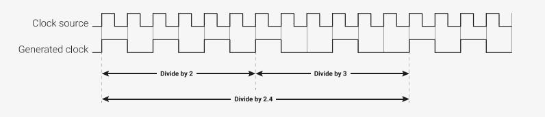
A timing diagram illustrating fractional division. It shows a 'Clock source' as a regular square wave. Below it, the 'Generated clock' is shown as a square wave that changes its period. Horizontal arrows indicate the division factors: 'Divide by 2' for the first segment, 'Divide by 3' for the second segment, and 'Divide by 2.4' for the third segment. The generated clock's period increases when the divisor increases and decreases when the divisor decreases.
All dividers support on-the-fly divisor changes meaning the output clock will switch cleanly from one divisor to another. The clock generator does not need to be stopped during clock divisor changes. It does this by synchronising the divisor change to the end of the clock cycle. Similarly, the enable is synchronised to the end of the clock cycle so will not generate glitches when the clock generator is enabled or disabled. Clock generators for always-on clocks are permanently enabled and therefore do not have an enable control.
In the event that a clock generator locks up and never completes the current clock cycle it can be forced to stop using the KILL control. This may result in an output glitch which may corrupt the logic driven by the clock. It is therefore recommended the destination logic is reset prior to this operation. It is worth mentioning that this clock generator design has been used in numerous chips and has never been known to lock up. The KILL control is inelegant and unnecessary and should not be used as an alternative to the enable. Clock generators for always-on clocks are permanently active and therefore do not have a KILL control.
2.15.3.4. Duty Cycle Correction
The divider operates on the rising edge of the input clock and so does not generate an even duty cycle clock when dividing by odd numbers.
Divide by 3 will give a duty cycle of 33.3%, divide by 5 will be 40% etc. If enabled, the duty cycle correction logic will shift the falling edge of the output clock to the falling edge of the input clock and restore a 50% duty cycle. The duty cycle correction can be enabled and disabled while the clock is running. It will not operate when dividing by an even number.
Figure 32. An example of duty_cycle_correction.
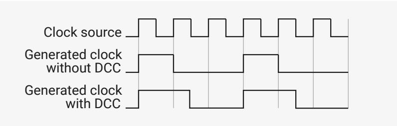
A timing diagram illustrating duty cycle correction. It shows three waveforms: 'Clock source' (a regular square wave), 'Generated clock without DCC' (a square wave with a duty cycle less than 50%), and 'Generated clock with DCC' (a square wave with a 50% duty cycle). The 'Generated clock with DCC' waveform is shifted so that its falling edges align with the falling edges of the 'Clock source'.
2.15.3.5. Clock Enables
Each clock goes to multiple destinations and, with a few exceptions, there are 2 enables for each destination. The
WAKE_EN
registers are used to enable the clocks when the system is awake and the
SLEEP_EN
registers are used to enable the clocks when the system is in sleep mode. The purpose of these enables is to reduce power in the clock distribution networks for components that are not being used. It is worth noting that a component which is not clocked will retain its configuration so can be restarted quickly.
NOTE
The
WAKE_EN
and
SLEEP_EN
registers reset to
0x1
, which means that by default all clocks are enabled. The programmer only needs to use this feature if they desire a low-power design.
2.15.3.5.1. Clock Enable Exceptions
The processor cores do not have clock enables because they require a clock at all times to manage their own power saving features.
clk_sys_busfabric
cannot be disabled in wake mode because that would prevent the cores from accessing any chip registers, including those that control the clock enables.
clk_sys_clocks
does not have a wake mode enable because disabling it would prevent the cores from accessing the clocks control registers.
The gpclks do not have clock enables.
2.15.3.5.2. System Sleep Mode
System sleep mode is entered automatically when both cores are in sleep and the DMA has no outstanding transactions. In system sleep mode, the clock enables described in the previous paragraphs are switched from the
WAKE_EN
registers to the
SLEEP_EN
registers. The intention is to reduce power consumed in the clock distribution networks when the chip is inactive. If the user has not configured the
WAKE_EN
and
SLEEP_EN
registers then system sleep will do nothing.
There is little value in using system sleep without taking other measures to reduce power before the cores are put to sleep. Things to consider include:
- • stop unused clock sources such as the PLLs and Crystal Oscillator
- • reduce the frequencies of generated clocks by increasing the clock divisors
- • stop external clocks
For maximum power saving when the chip is inactive, the user should consider DORMANT (see Section 2.11.3 ) mode in which clocks are sourced from the Crystal Oscillator and/or the Ring Oscillator and those clock sources are stopped.
2.15.4. Frequency Counter
The frequency counter measures the frequency of internal and external clocks by counting the clock edges seen over a test interval. The interval is defined by counting cycles of
clk_ref
which must be driven either from XOSC or from a stable external source of known frequency.
The user can pick between accuracy and test time using the
FC0_INTERVAL
register.
Table 206
shows the trade off.
Table 206. Frequency Counter Test Interval vs Accuracy
| Interval Register | Test Interval | Accuracy |
|---|---|---|
| 0 | 1µs | 2048kHz |
| 1 | 2µs | 1024kHz |
| 2 | 4µs | 512kHz |
| 3 | 8µs | 256kHz |
| 4 | 16µs | 128kHz |
| 5 | 32µs | 64kHz |
| 6 | 64µs | 32kHz |
| 7 | 125µs | 16kHz |
| 8 | 250µs | 8kHz |
| 9 | 500µs | 4kHz |
| 10 | 1ms | 2kHz |
| 11 | 2ms | 1kHz |
| 12 | 4ms | 500Hz |
| 13 | 8ms | 250Hz |
| Interval Register | Test Interval | Accuracy |
|---|---|---|
| 14 | 16ms | 125Hz |
| 15 | 32ms | 62.5Hz |
2.15.5. Resus
It is possible to write software that inadvertently stops
clk_sys
. This will normally cause an unrecoverable lock-up of the cores and the on-chip debugger, leaving the user unable to trace the problem. To mitigate against that, an automatic resuscitation circuit is provided which will switch
clk_sys
to a known good clock source if no edges are detected over a user-defined interval. The known good source is
clk_ref
which can be driven from the XOSC, ROSC or an external source.
The resus block counts edges on
clk_sys
during a timeout interval controlled by
clk_ref
, and forces
clk_sys
to be driven from
clk_ref
if no
clk_sys
edges are detected. The interval is programmable via
CLK_SYS_RESUS_CTRL
.
⚠ WARNING
There is no way for resus to revive the chip if
clk_ref
is also stopped.
To enable the resus, the programmer must set the timeout interval and then set the
ENABLE
bit in
CLK_SYS_RESUS_CTRL
. To detect a resus event, the
CLK_SYS_RESUS
interrupt must be enabled by setting the interrupt enable bit in
INTE
. The
CLOCKS_DEFAULT_IRQ
(see
Section 2.3.2
) must also be enabled at the processor.
Resus is intended as a debugging aid. The intention is for the user to trace the software error that triggered the resus, then correct the error and reboot. It is possible to continue running after a resus event by reconfiguring
clk_sys
then clearing the resus by writing the
CLEAR
bit in
CLK_SYS_RESUS_CTRL
. However, it should be noted that a resus can be triggered by
clk_sys
running more slowly than expected and that could result in a
clk_sys
glitch when resus is triggered. That glitch could corrupt the chip. This would be a rare event but is tolerable in a debugging scenario. However it is unacceptable in normal operation therefore it is recommended to only use resus for debug.
⚠ WARNING
Resus is a debugging aid and should not be used as a means of switching clocks in normal operation.
2.15.6. Programmer's Model
2.15.6.1. Configuring a clock generator
The SDK defines an enum of clocks:
SDK: https://github.com/raspberrypi/pico-sdk/blob/master/src/rp2040/hardware_structs/include/hardware/structs/clocks.h Lines 30 - 42
30 typedef enum clock_num_rp2040 {
31     clk_gpout0 = 0, ///< Select CLK_GPOUT0 as clock source
32     clk_gpout1 = 1, ///< Select CLK_GPOUT1 as clock source
33     clk_gpout2 = 2, ///< Select CLK_GPOUT2 as clock source
34     clk_gpout3 = 3, ///< Select CLK_GPOUT3 as clock source
35     clk_ref = 4,   ///< Select CLK_REF as clock source
36     clk_sys = 5,   ///< Select CLK_SYS as clock source
37     clk_peri = 6,  ///< Select CLK_PERI as clock source
38     clk_usb = 7,   ///< Select CLK_USB as clock source
39     clk_adc = 8,   ///< Select CLK_ADC as clock source
40     clk_rtc = 9,   ///< Select CLK_RTC as clock source
41     CLK_COUNT
42 } clock_num_t;
And also a struct to describe the registers of a clock generator:
SDK: https://github.com/raspberrypi/pico-sdk/blob/master/src/rp2040/hardware_structs/include/hardware/structs/clocks.h Lines 100 - 121
100 typedef struct {
101     _REG_(CLOCKS_CLK_GPOUT0_CTRL_OFFSET) // CLOCKS_CLK_GPOUT0_CTRL
102     // Clock control, can be changed on-the-fly (except for auxsrc)
103     // 0x00100000 [20]  NUDGE      (0) An edge on this signal shifts the phase of the
        output by...
104     // 0x00030000 [17:16] PHASE      (0x0) This delays the enable signal by up to 3 cycles
        of the...
105     // 0x00001000 [12]    DC50      (0) Enables duty cycle correction for odd divisors
106     // 0x00000800 [11]    ENABLE     (0) Starts and stops the clock generator cleanly
107     // 0x00000400 [10]    KILL      (0) Asynchronously kills the clock generator
108     // 0x000001e0 [8:5]   AUXSRC     (0x0) Selects the auxiliary clock source, will glitch
        when switching
109     io_rw_32 ctrl;
110
111     _REG_(CLOCKS_CLK_GPOUT0_DIV_OFFSET) // CLOCKS_CLK_GPOUT0_DIV
112     // Clock divisor, can be changed on-the-fly
113     // 0xffffffff00 [31:8] INT      (0x000001) Integer component of the divisor, 0 ->
        divide by 2^16
114     // 0x000000ff [7:0]   FRAC      (0x00) Fractional component of the divisor
115     io_rw_32 div;
116
117     _REG_(CLOCKS_CLK_GPOUT0_SELECTED_OFFSET) // CLOCKS_CLK_GPOUT0_SELECTED
118     // Indicates which SRC is currently selected by the glitchless mux (one-hot)
119     // 0xffffffff [31:0] CLK_GPOUT0_SELECTED (0x00000001) This slice does not have a
        glitchless mux (only the...
120     io_ro_32 selected;
121 } clock_hw_t;
To configure a clock, we need to know the following pieces of information:
- • The frequency of the clock source
- • The mux / aux mux position of the clock source
- • The desired output frequency
The SDK provides
clock_configure
to configure a clock:
SDK: https://github.com/raspberrypi/pico-sdk/blob/master/src/rp2_common/hardware_clocks/clocks.c Lines 40 - 133
40 static void clock_configure_internal(clock_handle_t clock, uint32_t src, uint32_t auxsrc,
    uint32_t actual_freq, uint32_t div) {
41     clock_hw_t *clock_hw = &clocks_hw->clk[clock];
42
43     // If increasing divisor, set divisor before source. Otherwise set source
44     // before divisor. This avoids a momentary overspeed when e.g. switching
45     // to a faster source and increasing divisor to compensate.
46     if (div > clock_hw->div)
47         clock_hw->div = div;
48
49     // If switching a glitchless slice (ref or sys) to an aux source, switch
50     // away from aux *first* to avoid passing glitches when changing aux mux.
51     // Assume (!!!) glitchless source 0 is no faster than the aux source.
52     if (has_glitchless_mux(clock) && src ==
        CLOCKS_CLK_SYS_CTRL_SRC_VALUE_CLKSRC_CLK_SYS_AUX) {
53         hw_clear_bits(&clock_hw->ctrl, CLOCKS_CLK_REF_CTRL_SRC_BITS);
54     while (!(clock_hw->selected & 1u))
55         tight_loop_contents();
56     }
57     // If no glitchless mux, cleanly stop the clock to avoid glitches
58     // propagating when changing aux mux. Note it would be a really bad idea
59     // to do this on one of the glitchless clocks (clk_sys, clk_ref).
60     else {
61         // Disable clock. On clk_ref and clk_sys this does nothing,
62         // all other clocks have the ENABLE bit in the same position.
63         hw_clear_bits(&clock_hw->ctrl, CLOCKS_CLK_GPOUT0_CTRL_ENABLE_BITS);
64         if (configured_freq[clock] > 0) {
65             // Delay for 3 cycles of the target clock, for ENABLE propagation.
66             // Note XOSC_COUNT is not helpful here because XOSC is not
67             // necessarily running, nor is timer...
68             uint delay_cyc = configured_freq[clk_sys] / configured_freq[clock] + 1;
69             busy_wait_at_least_cycles(delay_cyc * 3);
70         }
71     }
72
73     // Set aux mux first, and then glitchless mux if this clock has one
74     hw_write_masked(&clock_hw->ctrl,
75         (auxsrc << CLOCKS_CLK_SYS_CTRL_AUXSRC_LSB),
76         CLOCKS_CLK_SYS_CTRL_AUXSRC_BITS
77     );
78
79     if (has_glitchless_mux(clock)) {
80         hw_write_masked(&clock_hw->ctrl,
81             src << CLOCKS_CLK_REF_CTRL_SRC_LSB,
82             CLOCKS_CLK_REF_CTRL_SRC_BITS
83         );
84         while (!(clock_hw->selected & (1u << src)))
85             tight_loop_contents();
86     }
87
88     // Enable clock. On clk_ref and clk_sys this does nothing,
89     // all other clocks have the ENABLE bit in the same position.
90     hw_set_bits(&clock_hw->ctrl, CLOCKS_CLK_GPOUT0_CTRL_ENABLE_BITS);
91
92     // Now that the source is configured, we can trust that the user-supplied
93     // divisor is a safe value.
94     clock_hw->div = div;
95     configured_freq[clock] = actual_freq;
96 }
97
98 bool clock_configure(clock_handle_t clock, uint32_t src, uint32_t auxsrc, uint32_t src_freq,
99     uint32_t freq) {
100     assert(src_freq >= freq);
101
102     if (freq > src_freq)
103         return false;
104
105     uint64_t div64 = (((uint64_t) src_freq) << CLOCKS_CLK_GPOUT0_DIV_INT_LSB) / freq;
106     uint32_t div, actual_freq;
107     if (div64 >> 32) {
108         // set div to 0 for maximum clock divider
109         div = 0;
110         actual_freq = src_freq >> (32 - CLOCKS_CLK_GPOUT0_DIV_INT_LSB);
111     } else {
112         div = (uint32_t) div64;
113         // on RP2040 only clock divider of 1, or >= 2 are supported
114         if (div < (2u << CLOCKS_CLK_GPOUT0_DIV_INT_LSB)) {
115             div = (1u << CLOCKS_CLK_GPOUT0_DIV_INT_LSB);
116         }
117         actual_freq = (uint32_t) (((uint64_t) src_freq) << CLOCKS_CLK_GPOUT0_DIV_INT_LSB) /
        div);
117     }
118
119     clock_configure_internal(clock, src, auxsrc, actual_freq, div);
120     // Store the configured frequency
121     return true;
122 }
123
124 void clock_configure_int_divider(clock_handle_t clock, uint32_t src, uint32_t auxsrc,
uint32_t src_freq, uint32_t int_divider) {
125     clock_configure_internal(clock, src, auxsrc, src_freq / int_divider, int_divider <<
CLOCKS_CLK_GPOUT0_DIV_INT_LSB);
126 }
127
128 void clock_configure_undivided(clock_handle_t clock, uint32_t src, uint32_t auxsrc, uint32_t
src_freq) {
129     clock_configure_internal(clock, src, auxsrc, src_freq, 1u <<
CLOCKS_CLK_GPOUT0_DIV_INT_LSB);
130 }
It is called in
clocks_init
for each clock. The following example shows the
clk_sys
configuration:
SDK: https://github.com/raspberrypi/pico-sdk/blob/master/src/rp2_common/pico_runtime_init/runtime_init_clocks.c Lines 100 - 104
100     // CLK SYS = PLL SYS (usually) 125MHz / 1 = 125MHz
101     clock_configure_undivided(clk_sys,
102                             CLOCKS_CLK_SYS_CTRL_SRC_VALUE_CLKSRC_CLK_SYS_AUX,
103                             CLOCKS_CLK_SYS_CTRL_AUXSRC_VALUE_CLKSRC_PLL_SYS,
104                             SYS_CLK_HZ);
Once a clock is configured,
clock_get_hz
can be called to get the output frequency in Hz.
SDK: https://github.com/raspberrypi/pico-sdk/blob/master/src/rp2_common/hardware_clocks/clocks.c Lines 137 - 139
137 uint32_t clock_get_hz(clock_handle_t clock) {
138     return configured_freq[clock];
139 }
⚠ WARNING
It is assumed the source frequency the programmer provides is correct. If it is not then the frequency returned by
clock_get_hz
will be inaccurate.
2.15.6.2. Using the frequency counter
To use the frequency counter, the programmer must:
- • Set the reference frequency:
clk_ref - • Set the mux position of the source they want to measure. See FC0_SRC
- • Wait for the
DONEstatus bit in FC0_STATUS to be set - • Read the result
The SDK defines a
frequency_count
function which takes the source as an argument and returns the frequency in kHz:
SDK: https://github.com/raspberrypi/pico-sdk/blob/master/src/rp2_common/hardware_clocks/clocks.c Lines 147 - 174
147 uint32_t frequency_count_khz(uint src) {
148     fc_hw_t *fc = &clocks_hw->fc0;
149
150     // If frequency counter is running need to wait for it. It runs even if the source is NULL
151     while(fc->status & CLOCKS_FC0_STATUS_RUNNING_BITS) {
152         tight_loop_contents();
153     }
154
155     // Set reference freq
156     fc->ref_khz = clock_get_hz(clk_ref) / 1000;
157
158     // FIXME: Don't pick random interval. Use best interval
159     fc->interval = 10;
160
161     // No min or max
162     fc->min_khz = 0;
163     fc->max_khz = 0xffffffff;
164
165     // Set SRC which automatically starts the measurement
166     fc->src = src;
167
168     while(!(fc->status & CLOCKS_FC0_STATUS_DONE_BITS)) {
169         tight_loop_contents();
170     }
171
172     // Return the result
173     return fc->result >> CLOCKS_FC0_RESULT_KHZ_LSB;
174 }
There is also a wrapper function to change the unit to MHz:
SDK: https://github.com/raspberrypi/pico-sdk/blob/master/src/rp2_common/hardware_clocks/include/hardware/clocks.h Lines 377 - 379
377 static inline float frequency_count_mhz(uint src) {
378     return ((float) (frequency_count_khz(src))) / KHZ;
379 }
i NOTE
The frequency counter can also be used in a test mode. This allows the hardware to check if the frequency is within a minimum frequency and a maximum frequency, set in FC0_MIN_KHZ and FC0_MAX_KHZ . In this mode, the PASS bit in FC0_STATUS will be set when DONE is set if the frequency is within the specified range. Otherwise, either the FAST or SLOW bit will be set.
If the programmer attempts to count a stopped clock, or the clock stops running then the DIED bit will be set. If any of DIED , FAST , or SLOW are set then FAIL will be set.
2.15.6.3. Configuring a GPIO output clock
SDK: https://github.com/raspberrypi/pico-sdk/blob/master/src/rp2_common/hardware_clocks/clocks.c Lines 245 - 276
245 void clock_gpio_init_int_frac16(uint gpio, uint src, uint32_t div_int, uint16_t div_frac16)
246 {
247     // Bit messy but it's as much code to loop through a lookup
248     // table. The sources for each gpout generators are the same
248 // so just call with the sources from GP0
249 uint gpclk = 0;
250 if (gpio == 21) gpclk = clk_gpout0;
251 else if (gpio == 23) gpclk = clk_gpout1;
252 else if (gpio == 24) gpclk = clk_gpout2;
253 else if (gpio == 25) gpclk = clk_gpout3;
254 else {
255     invalid_params_if(HARDWARE_CLOCKS, true);
256 }
257
258 invalid_params_if(HARDWARE_CLOCKS, div_int >> REG_FIELD_WIDTH(
    CLOCKS_CLK_GPOUT0_DIV_INT));
259 // Set up the gpclk generator
260 clocks_hw->clk[gpclk].ctrl = (src << CLOCKS_CLK_GPOUT0_CTRL_AUXSRC_LSB) |
261     CLOCKS_CLK_GPOUT0_CTRL_ENABLE_BITS;
262 #ifdef REG_FIELD_WIDTH(CLOCKS_CLK_GPOUT0_DIV_FRAC) == 16
263     clocks_hw->clk[gpclk].div = (div_int << CLOCKS_CLK_GPOUT0_DIV_INT_LSB) | (div_frac16 <<
        CLOCKS_CLK_GPOUT0_DIV_FRAC_LSB);
264 #elif REG_FIELD_WIDTH(CLOCKS_CLK_GPOUT0_DIV_FRAC) == 8
265     clocks_hw->clk[gpclk].div = (div_int << CLOCKS_CLK_GPOUT0_DIV_INT_LSB) | ((div_frac16
        >> 8u) << CLOCKS_CLK_GPOUT0_DIV_FRAC_LSB);
266 #else
267 #error unsupported number of fractional bits
268 #endif
269
270 // Set gpio pin to gpclock function
271 gpio_set_function(gpio, GPIO_FUNC_GPCK);
272 }
2.15.6.4. Configuring a GPIO input clock
SDK: https://github.com/raspberrypi/pico-sdk/blob/master/src/rp2-common/hardware_clocks/clocks.c Lines 313 - 343
313 bool clock_configure_gpin(clock_handle_t clock, uint gpio, uint32_t src_freq, uint32_t freq)
314 {
315     // Configure a clock to run from a GPIO input
316     uint gpin = 0;
317     if (gpio == 20) gpin = 0;
318     else if (gpio == 22) gpin = 1;
319     else {
320         invalid_params_if(HARDWARE_CLOCKS, true);
321     }
322
323     // Work out sources. GPIN is always an auxsrc
324     uint src = 0;
325
326     // GPIN1 == GPIN0 + 1
327     uint auxsrc = gpin0_src[clock] + gpin;
328
329     if (has_glitchless_mux(clock)) {
330         // AUX src is always 1
331         src = 1;
332     }
333
334     // Set the GPIO function
335     gpio_set_function(gpio, GPIO_FUNC_GPCK);
336
337     // Now we have the src, auxsrc, and configured the gpio input
338     // call clock configure to run the clock from a gpio
339     return clock_configure(clock, src, auxsrc, src_freq, freq);
339 }
2.15.6.5. Enabling resus
SDK: https://github.com/raspberrypi/pico-sdk/blob/master/src/rp2_common/hardware_clocks/clocks.c Lines 221 - 243
221 void clocks_enable_resus(resus_callback_t resus_callback) {
222     // Restart clk_sys if it is stopped by forcing it
223     // to the default source of clk_ref. If clk_ref stops running this will
224     // not work.
225
226     // Store user's resus callback
227     _resus_callback = resus_callback;
228
229     irq_set_exclusive_handler(CLOCKS_IRQ, clocks_irq_handler);
230
231     // Enable the resus interrupt in clocks
232     clocks_hw->inte = CLOCKS_INTE_CLK_SYS_RESUS_BITS;
233
234     // Enable the clocks irq
235     irq_set_enabled(CLOCKS_IRQ, true);
236
237     // 2 * clk_ref freq / clk_sys_min_freq;
238     // assume clk_ref is 3MHz and we want clk_sys to be no lower than 1MHz
239     uint timeout = 2 * 3 * 1;
240
241     // Enable resus with the maximum timeout
242     clocks_hw->resus.ctrl = CLOCKS_CLK_SYS_RESUS_CTRL_ENABLE_BITS | timeout;
243 }
2.15.6.6. Configuring sleep mode
Sleep mode is active when neither processor core or the DMA are requesting clocks. For example, the DMA is not active and both
core0
and
core1
are waiting for an interrupt. The
SLEEP_EN
registers set what clocks are running in sleep mode. The
hello_sleep
example (
https://github.com/raspberrypi/pico-playground/blob/master/sleep/hello_sleep/hello_sleep_aon.c
) illustrates how to put the chip to sleep until the RTC fires. In this case, only the RTC clock is enabled in the
SLEEP_EN0
register.
i NOTE
clk_sys
is always sent to
proc0
and
proc1
during sleep mode as some logic needs to be clocked for the processor to wake up again.
Pico Extras: https://github.com/raspberrypi/pico-extras/blob/master/src/rp2_common/pico_sleep/sleep.c Lines 159 - 183
159 void sleep_goto_sleep_until(struct timespec *ts, aon_timer_alarm_handler_t callback)
160 {
161
162     // We should have already called the sleep_run_from_dormant_source function
163     // This is only needed for dormancy although it saves power running from xosc while
164     // sleeping
165     //assert(dormant_source_valid(_dormant_source));
166
167     clocks_hw->sleep_en0 = CLOCKS_SLEEP_EN0_CLK_RTC_RTC_BITS;
168     clocks_hw->sleep_en1 = 0x0;
168 169 aon_timer_enable_alarm(ts, callback, false); 170 171 stdio_flush(); 172 173 // Enable deep sleep at the proc 174 processor_deep_sleep(); 175 176 // Go to sleep 177 __wfi(); 178 }
2.15.7. List of Registers
The Clocks registers start at a base address of
0x40008000
(defined as
CLOCKS_BASE
in SDK).
Table 207. List of CLOCKS registers
| Offset | Name | Info |
|---|---|---|
| 0x00 | CLK_GPOUT0_CTRL | Clock control, can be changed on-the-fly (except for auxsrc) |
| 0x04 | CLK_GPOUT0_DIV | Clock divisor, can be changed on-the-fly |
| 0x08 | CLK_GPOUT0_SELECTED | Indicates which SRC is currently selected by the glitchless mux (one-hot). |
| 0x0c | CLK_GPOUT1_CTRL | Clock control, can be changed on-the-fly (except for auxsrc) |
| 0x10 | CLK_GPOUT1_DIV | Clock divisor, can be changed on-the-fly |
| 0x14 | CLK_GPOUT1_SELECTED | Indicates which SRC is currently selected by the glitchless mux (one-hot). |
| 0x18 | CLK_GPOUT2_CTRL | Clock control, can be changed on-the-fly (except for auxsrc) |
| 0x1c | CLK_GPOUT2_DIV | Clock divisor, can be changed on-the-fly |
| 0x20 | CLK_GPOUT2_SELECTED | Indicates which SRC is currently selected by the glitchless mux (one-hot). |
| 0x24 | CLK_GPOUT3_CTRL | Clock control, can be changed on-the-fly (except for auxsrc) |
| 0x28 | CLK_GPOUT3_DIV | Clock divisor, can be changed on-the-fly |
| 0x2c | CLK_GPOUT3_SELECTED | Indicates which SRC is currently selected by the glitchless mux (one-hot). |
| 0x30 | CLK_REF_CTRL | Clock control, can be changed on-the-fly (except for auxsrc) |
| 0x34 | CLK_REF_DIV | Clock divisor, can be changed on-the-fly |
| 0x38 | CLK_REF_SELECTED | Indicates which SRC is currently selected by the glitchless mux (one-hot). |
| 0x3c | CLK_SYS_CTRL | Clock control, can be changed on-the-fly (except for auxsrc) |
| 0x40 | CLK_SYS_DIV | Clock divisor, can be changed on-the-fly |
| 0x44 | CLK_SYS_SELECTED | Indicates which SRC is currently selected by the glitchless mux (one-hot). |
| 0x48 | CLK_PERI_CTRL | Clock control, can be changed on-the-fly (except for auxsrc) |
| 0x50 | CLK_PERI_SELECTED | Indicates which SRC is currently selected by the glitchless mux (one-hot). |
| Offset | Name | Info |
|---|---|---|
| 0x54 | CLK_USB_CTRL | Clock control, can be changed on-the-fly (except for auxsrc) |
| 0x58 | CLK_USB_DIV | Clock divisor, can be changed on-the-fly |
| 0x5c | CLK_USB_SELECTED | Indicates which SRC is currently selected by the glitchless mux (one-hot). |
| 0x60 | CLK_ADC_CTRL | Clock control, can be changed on-the-fly (except for auxsrc) |
| 0x64 | CLK_ADC_DIV | Clock divisor, can be changed on-the-fly |
| 0x68 | CLK_ADC_SELECTED | Indicates which SRC is currently selected by the glitchless mux (one-hot). |
| 0x6c | CLK_RTC_CTRL | Clock control, can be changed on-the-fly (except for auxsrc) |
| 0x70 | CLK_RTC_DIV | Clock divisor, can be changed on-the-fly |
| 0x74 | CLK_RTC_SELECTED | Indicates which SRC is currently selected by the glitchless mux (one-hot). |
| 0x78 | CLK_SYS_RESUS_CTRL | |
| 0x7c | CLK_SYS_RESUS_STATUS | |
| 0x80 | FC0_REF_KHZ | Reference clock frequency in kHz |
| 0x84 | FC0_MIN_KHZ | Minimum pass frequency in kHz. This is optional. Set to 0 if you are not using the pass/fail flags |
| 0x88 | FC0_MAX_KHZ | Maximum pass frequency in kHz. This is optional. Set to 0x1fffff if you are not using the pass/fail flags |
| 0x8c | FC0_DELAY | Delays the start of frequency counting to allow the mux to settle Delay is measured in multiples of the reference clock period |
| 0x90 | FC0_INTERVAL | The test interval is
\(
0.98\mu s * 2^{**}interval
\)
, but let's call it
\(
1\mu s * 2^{**}interval
\) The default gives a test interval of 250us |
| 0x94 | FC0_SRC | Clock sent to frequency counter, set to 0 when not required Writing to this register initiates the frequency count |
| 0x98 | FC0_STATUS | Frequency counter status |
| 0x9c | FC0_RESULT | Result of frequency measurement, only valid when status_done=1 |
| 0xa0 | WAKE_EN0 | enable clock in wake mode |
| 0xa4 | WAKE_EN1 | enable clock in wake mode |
| 0xa8 | SLEEP_EN0 | enable clock in sleep mode |
| 0xac | SLEEP_EN1 | enable clock in sleep mode |
| 0xb0 | ENABLED0 | indicates the state of the clock enable |
| 0xb4 | ENABLED1 | indicates the state of the clock enable |
| 0xb8 | INTR | Raw Interrupts |
| 0xbc | INTE | Interrupt Enable |
| 0xc0 | INTF | Interrupt Force |
| 0xc4 | INTS | Interrupt status after masking & forcing |
Clock control, can be changed on-the-fly (except for auxsrc)
Table 208.CLK_GPOUT0_CTRL
Register
| Bits | Description | Type | Reset |
|---|---|---|---|
| 31:21 | Reserved. | - | - |
| 20 | NUDGE:
An edge on this signal shifts the phase of the output by 1 cycle of the input clock This can be done at any time | RW | 0x0 |
| 19:18 | Reserved. | - | - |
| 17:16 | PHASE:
This delays the enable signal by up to 3 cycles of the input clock This must be set before the clock is enabled to have any effect | RW | 0x0 |
| 15:13 | Reserved. | - | - |
| 12 | DC50: Enables duty cycle correction for odd divisors | RW | 0x0 |
| 11 | ENABLE: Starts and stops the clock generator cleanly | RW | 0x0 |
| 10 | KILL: Asynchronously kills the clock generator | RW | 0x0 |
| 9 | Reserved. | - | - |
| 8:5 | AUXSRC: Selects the auxiliary clock source, will glitch when switching | RW | 0x0 |
| Enumerated values: | |||
| 0x0 → CLKSRC_PLL_SYS | |||
| 0x1 → CLKSRC_GPIN0 | |||
| 0x2 → CLKSRC_GPIN1 | |||
| 0x3 → CLKSRC_PLL_USB | |||
| 0x4 → ROSC_CLKSRC | |||
| 0x5 → XOSC_CLKSRC | |||
| 0x6 → CLK_SYS | |||
| 0x7 → CLK_USB | |||
| 0x8 → CLK_ADC | |||
| 0x9 → CLK_RTC | |||
| 0xa → CLK_REF | |||
| 4:0 | Reserved. | - | - |
Clock divisor, can be changed on-the-fly
Table 209.
CLK_GPOUT0_DIV
Register
| Bits | Description | Type | Reset |
|---|---|---|---|
| 31:8 | INT : Integer component of the divisor, 0 → divide by 2 16 | RW | 0x000001 |
| 7:0 | FRAC : Fractional component of the divisor | RW | 0x00 |
CLOCKS: CLK_GPOUT0_SELECTED Register
Offset: 0x08
Description
Indicates which SRC is currently selected by the glitchless mux (one-hot).
Table 210.
CLK_GPOUT0_SELECT
ED Register
| Bits | Description | Type | Reset |
|---|---|---|---|
| 31:0 | This slice does not have a glitchless mux (only the AUX_SRC field is present, not SRC) so this register is hardwired to 0x1. | RO | 0x00000001 |
CLOCKS: CLK_GPOUT1_CTRL Register
Offset: 0x0c
Description
Clock control, can be changed on-the-fly (except for auxsrc)
Table 211.
CLK_GPOUT1_CTRL
Register
| Bits | Description | Type | Reset |
|---|---|---|---|
| 31:21 | Reserved. | - | - |
| 20 | NUDGE
: An edge on this signal shifts the phase of the output by 1 cycle of the input clock This can be done at any time | RW | 0x0 |
| 19:18 | Reserved. | - | - |
| 17:16 | PHASE
: This delays the enable signal by up to 3 cycles of the input clock This must be set before the clock is enabled to have any effect | RW | 0x0 |
| 15:13 | Reserved. | - | - |
| 12 | DC50 : Enables duty cycle correction for odd divisors | RW | 0x0 |
| 11 | ENABLE : Starts and stops the clock generator cleanly | RW | 0x0 |
| 10 | KILL : Asynchronously kills the clock generator | RW | 0x0 |
| 9 | Reserved. | - | - |
| 8:5 | AUXSRC : Selects the auxiliary clock source, will glitch when switching | RW | 0x0 |
| Enumerated values: | |||
| 0x0 → CLKSRC_PLL_SYS | |||
| 0x1 → CLKSRC_GPIN0 | |||
| 0x2 → CLKSRC_GPIN1 | |||
| 0x3 → CLKSRC_PLL_USB | |||
| 0x4 → ROSC_CLKSRC | |||
| 0x5 → XOSC_CLKSRC | |||
| 0x6 → CLK_SYS | |||
| 0x7 → CLK_USB |
| Bits | Description | Type | Reset |
|---|---|---|---|
| 0x8 → CLK_ADC | |||
| 0x9 → CLK_RTC | |||
| 0xa → CLK_REF | |||
| 4:0 | Reserved. | - | - |
CLOCKS: CLK_GPOUT1_DIV Register
Offset: 0x10
Description
Clock divisor, can be changed on-the-fly
Table 212.
CLK_GPOUT1_DIV
Register
| Bits | Description | Type | Reset |
|---|---|---|---|
| 31:8 | INT : Integer component of the divisor, 0 → divide by 2 16 | RW | 0x000001 |
| 7:0 | FRAC : Fractional component of the divisor | RW | 0x00 |
CLOCKS: CLK_GPOUT1_SELECTED Register
Offset: 0x14
Description
Indicates which SRC is currently selected by the glitchless mux (one-hot).
Table 213.
CLK_GPOUT1_SELECTED
Register
| Bits | Description | Type | Reset |
|---|---|---|---|
| 31:0 | This slice does not have a glitchless mux (only the AUX_SRC field is present, not SRC) so this register is hardwired to 0x1. | RO | 0x00000001 |
CLOCKS: CLK_GPOUT2_CTRL Register
Offset: 0x18
Description
Clock control, can be changed on-the-fly (except for auxsrc)
Table 214.
CLK_GPOUT2_CTRL
Register
| Bits | Description | Type | Reset |
|---|---|---|---|
| 31:21 | Reserved. | - | - |
| 20 | NUDGE
: An edge on this signal shifts the phase of the output by 1 cycle of the input clock This can be done at any time | RW | 0x0 |
| 19:18 | Reserved. | - | - |
| 17:16 | PHASE
: This delays the enable signal by up to 3 cycles of the input clock This must be set before the clock is enabled to have any effect | RW | 0x0 |
| 15:13 | Reserved. | - | - |
| 12 | DC50 : Enables duty cycle correction for odd divisors | RW | 0x0 |
| 11 | ENABLE : Starts and stops the clock generator cleanly | RW | 0x0 |
| 10 | KILL : Asynchronously kills the clock generator | RW | 0x0 |
| 9 | Reserved. | - | - |
| Bits | Description | Type | Reset |
|---|---|---|---|
| 8:5 | AUXSRC : Selects the auxiliary clock source, will glitch when switching | RW | 0x0 |
| Enumerated values: | |||
| 0x0 → CLKSRC_PLL_SYS | |||
| 0x1 → CLKSRC_GPIN0 | |||
| 0x2 → CLKSRC_GPIN1 | |||
| 0x3 → CLKSRC_PLL_USB | |||
| 0x4 → ROSC_CLKSRC_PH | |||
| 0x5 → XOSC_CLKSRC | |||
| 0x6 → CLK_SYS | |||
| 0x7 → CLK_USB | |||
| 0x8 → CLK_ADC | |||
| 0x9 → CLK_RTC | |||
| 0xa → CLK_REF | |||
| 4:0 | Reserved. | - | - |
CLOCKS: CLK_GPOUT2_DIV Register
Offset: 0x1c
Description
Clock divisor, can be changed on-the-fly
Table 215.
CLK_GPOUT2_DIV
Register
| Bits | Description | Type | Reset |
|---|---|---|---|
| 31:8 | INT : Integer component of the divisor, 0 → divide by 2 16 | RW | 0x000001 |
| 7:0 | FRAC : Fractional component of the divisor | RW | 0x00 |
CLOCKS: CLK_GPOUT2_SELECTED Register
Offset: 0x20
Description
Indicates which SRC is currently selected by the glitchless mux (one-hot).
Table 216.
CLK_GPOUT2_SELECTED
Register
| Bits | Description | Type | Reset |
|---|---|---|---|
| 31:0 | This slice does not have a glitchless mux (only the AUX_SRC field is present, not SRC) so this register is hardwired to 0x1. | RO | 0x00000001 |
CLOCKS: CLK_GPOUT3_CTRL Register
Offset: 0x24
Description
Clock control, can be changed on-the-fly (except for auxsrc)
Table 217.
CLK_GPOUT3_CTRL
Register
| Bits | Description | Type | Reset |
|---|---|---|---|
| 31:21 | Reserved. | - | - |
| Bits | Description | Type | Reset |
|---|---|---|---|
| 20 | NUDGE
: An edge on this signal shifts the phase of the output by 1 cycle of the input clock This can be done at any time | RW | 0x0 |
| 19:18 | Reserved. | - | - |
| 17:16 | PHASE
: This delays the enable signal by up to 3 cycles of the input clock This must be set before the clock is enabled to have any effect | RW | 0x0 |
| 15:13 | Reserved. | - | - |
| 12 | DC50 : Enables duty cycle correction for odd divisors | RW | 0x0 |
| 11 | ENABLE : Starts and stops the clock generator cleanly | RW | 0x0 |
| 10 | KILL : Asynchronously kills the clock generator | RW | 0x0 |
| 9 | Reserved. | - | - |
| 8:5 | AUXSRC : Selects the auxiliary clock source, will glitch when switching | RW | 0x0 |
| Enumerated values: | |||
| 0x0 → CLKSRC_PLL_SYS | |||
| 0x1 → CLKSRC_GPIN0 | |||
| 0x2 → CLKSRC_GPIN1 | |||
| 0x3 → CLKSRC_PLL_USB | |||
| 0x4 → ROSC_CLKSRC_PH | |||
| 0x5 → XOSC_CLKSRC | |||
| 0x6 → CLK_SYS | |||
| 0x7 → CLK_USB | |||
| 0x8 → CLK_ADC | |||
| 0x9 → CLK_RTC | |||
| 0xa → CLK_REF | |||
| 4:0 | Reserved. | - | - |
CLOCKS: CLK_GPOUT3_DIV Register
Offset: 0x28
Description
Clock divisor, can be changed on-the-fly
Table 218.
CLK_GPOUT3_DIV
Register
| Bits | Description | Type | Reset |
|---|---|---|---|
| 31:8 | INT : Integer component of the divisor, 0 → divide by 2 16 | RW | 0x000001 |
| 7:0 | FRAC : Fractional component of the divisor | RW | 0x00 |
CLOCKS: CLK_GPOUT3_SELECTED Register
Offset: 0x2c
DescriptionIndicates which SRC is currently selected by the glitchless mux (one-hot).
Table 219.
CLK_GPOUT3_SELECT
ED Register
| Bits | Description | Type | Reset |
|---|---|---|---|
| 31:0 | This slice does not have a glitchless mux (only the AUX_SRC field is present, not SRC) so this register is hardwired to 0x1. | RO | 0x00000001 |
Offset: 0x30
DescriptionClock control, can be changed on-the-fly (except for auxsrc)
Table 220.
CLK_REF_CTRL
Register
| Bits | Description | Type | Reset |
|---|---|---|---|
| 31:7 | Reserved. | - | - |
| 6:5 | AUXSRC: Selects the auxiliary clock source, will glitch when switching | RW | 0x0 |
| Enumerated values: | |||
| 0x0 → CLKSRC_PLL_USB | |||
| 0x1 → CLKSRC_GPIN0 | |||
| 0x2 → CLKSRC_GPIN1 | |||
| 4:2 | Reserved. | - | - |
| 1:0 | SRC: Selects the clock source glitchlessly, can be changed on-the-fly | RW | - |
| Enumerated values: | |||
| 0x0 → ROSC_CLKSRC_PH | |||
| 0x1 → CLKSRC_CLK_REF_AUX | |||
| 0x2 → XOSC_CLKSRC |
Offset: 0x34
DescriptionClock divisor, can be changed on-the-fly
Table 221.
CLK_REF_DIV Register
| Bits | Description | Type | Reset |
|---|---|---|---|
| 31:10 | Reserved. | - | - |
| 9:8 | INT: Integer component of the divisor, 0 → divide by 2 16 | RW | 0x1 |
| 7:0 | Reserved. | - | - |
Offset: 0x38
DescriptionIndicates which SRC is currently selected by the glitchless mux (one-hot).
Table 222.
CLK_REF_SELECTED
Register
| Bits | Description | Type | Reset |
|---|---|---|---|
| 31:0 | The glitchless multiplexer does not switch instantaneously (to avoid glitches), so software should poll this register to wait for the switch to complete. This register contains one decoded bit for each of the clock sources enumerated in the CTRL SRC field. At most one of these bits will be set at any time, indicating that clock is currently present at the output of the glitchless mux. Whilst switching is in progress, this register may briefly show all-0s. | RO | 0x00000001 |
CLOCKS: CLK_SYS_CTRL Register
Offset: 0x3c
Description
Clock control, can be changed on-the-fly (except for auxsrc)
Table 223.
CLK_SYS_CTRL
Register
| Bits | Description | Type | Reset |
|---|---|---|---|
| 31:8 | Reserved. | - | - |
| 7:5 | AUXSRC: Selects the auxiliary clock source, will glitch when switching | RW | 0x0 |
| Enumerated values: | |||
| 0x0 → CLKSRC_PLL_SYS | |||
| 0x1 → CLKSRC_PLL_USB | |||
| 0x2 → ROSC_CLKSRC | |||
| 0x3 → XOSC_CLKSRC | |||
| 0x4 → CLKSRC_GPIN0 | |||
| 0x5 → CLKSRC_GPIN1 | |||
| 4:1 | Reserved. | - | - |
| 0 | SRC: Selects the clock source glitchlessly, can be changed on-the-fly | RW | 0x0 |
| Enumerated values: | |||
| 0x0 → CLK_REF | |||
| 0x1 → CLKSRC_CLK_SYS_AUX |
CLOCKS: CLK_SYS_DIV Register
Offset: 0x40
Description
Clock divisor, can be changed on-the-fly
Table 224.
CLK_SYS_DIV Register
| Bits | Description | Type | Reset |
|---|---|---|---|
| 31:8 | INT: Integer component of the divisor, 0 → divide by 2 16 | RW | 0x000001 |
| 7:0 | FRAC: Fractional component of the divisor | RW | 0x00 |
CLOCKS: CLK_SYS_SELECTED Register
Offset: 0x44
Description
Indicates which SRC is currently selected by the glitchless mux (one-hot).
Table 225.
CLK_SYS_SELECTED
Register
| Bits | Description | Type | Reset |
|---|---|---|---|
| 31:0 | The glitchless multiplexer does not switch instantaneously (to avoid glitches), so software should poll this register to wait for the switch to complete. This register contains one decoded bit for each of the clock sources enumerated in the CTRL SRC field. At most one of these bits will be set at any time, indicating that clock is currently present at the output of the glitchless mux. Whilst switching is in progress, this register may briefly show all-0s. | RO | 0x00000001 |
CLOCKS: CLK_PERI_CTRL Register
Offset: 0x48
Description
Clock control, can be changed on-the-fly (except for auxsrc)
Table 226.
CLK_PERI_CTRL
Register
| Bits | Description | Type | Reset |
|---|---|---|---|
| 31:12 | Reserved. | - | - |
| 11 | ENABLE: Starts and stops the clock generator cleanly | RW | 0x0 |
| 10 | KILL: Asynchronously kills the clock generator | RW | 0x0 |
| 9:8 | Reserved. | - | - |
| 7:5 | AUXSRC: Selects the auxiliary clock source, will glitch when switching | RW | 0x0 |
| Enumerated values: | |||
| 0x0 → CLK_SYS | |||
| 0x1 → CLKSRC_PLL_SYS | |||
| 0x2 → CLKSRC_PLL_USB | |||
| 0x3 → ROOSC_CLKSRC_PH | |||
| 0x4 → XOOSC_CLKSRC | |||
| 0x5 → CLKSRC_GPIN0 | |||
| 0x6 → CLKSRC_GPIN1 | |||
| 4:0 | Reserved. | - | - |
CLOCKS: CLK_PERI_SELECTED Register
Offset: 0x50
Description
Indicates which SRC is currently selected by the glitchless mux (one-hot).
Table 227.
CLK_PERI_SELECTED
Register
| Bits | Description | Type | Reset |
|---|---|---|---|
| 31:0 | This slice does not have a glitchless mux (only the AUX_SRC field is present, not SRC) so this register is hardwired to 0x1. | RO | 0x00000001 |
CLOCKS: CLK_USB_CTRL Register
Offset: 0x54
Description
Clock control, can be changed on-the-fly (except for auxsrc)
Table 228.
CLK_USB_CTRL
Register
| Bits | Description | Type | Reset |
|---|---|---|---|
| 31:21 | Reserved. | - | - |
| 20 | NUDGE
: An edge on this signal shifts the phase of the output by 1 cycle of the input clock This can be done at any time | RW | 0x0 |
| 19:18 | Reserved. | - | - |
| 17:16 | PHASE
: This delays the enable signal by up to 3 cycles of the input clock This must be set before the clock is enabled to have any effect | RW | 0x0 |
| 15:12 | Reserved. | - | - |
| 11 | ENABLE : Starts and stops the clock generator cleanly | RW | 0x0 |
| 10 | KILL : Asynchronously kills the clock generator | RW | 0x0 |
| 9:8 | Reserved. | - | - |
| 7:5 | AUXSRC : Selects the auxiliary clock source, will glitch when switching | RW | 0x0 |
| Enumerated values: | |||
| 0x0 → CLKSRC_PLL_USB | |||
| 0x1 → CLKSRC_PLL_SYS | |||
| 0x2 → ROSC_CLKSRC_PH | |||
| 0x3 → XOSC_CLKSRC | |||
| 0x4 → CLKSRC_GPIN0 | |||
| 0x5 → CLKSRC_GPIN1 | |||
| 4:0 | Reserved. | - | - |
CLOCKS: CLK_USB_DIV Register
Offset: 0x58
Description
Clock divisor, can be changed on-the-fly
Table 229.
CLK_USB_DIV Register
| Bits | Description | Type | Reset |
|---|---|---|---|
| 31:10 | Reserved. | - | - |
| 9:8 | INT : Integer component of the divisor, 0 → divide by 2 16 | RW | 0x1 |
| 7:0 | Reserved. | - | - |
CLOCKS: CLK_USB_SELECTED Register
Offset: 0x5c
Description
Indicates which SRC is currently selected by the glitchless mux (one-hot).
Table 230.
CLK_USB_SELECTED
Register
| Bits | Description | Type | Reset |
|---|---|---|---|
| 31:0 | This slice does not have a glitchless mux (only the AUX_SRC field is present, not SRC) so this register is hardwired to 0x1. | RO | 0x00000001 |
CLOCKS: CLK_ADC_CTRL Register
Offset: 0x60
Description
Clock control, can be changed on-the-fly (except for auxsrc)
Table 231.
CLK_ADC_CTRL
Register
| Bits | Description | Type | Reset |
|---|---|---|---|
| 31:21 | Reserved. | - | - |
| 20 | NUDGE
: An edge on this signal shifts the phase of the output by 1 cycle of the input clock This can be done at any time | RW | 0x0 |
| 19:18 | Reserved. | - | - |
| 17:16 | PHASE
: This delays the enable signal by up to 3 cycles of the input clock This must be set before the clock is enabled to have any effect | RW | 0x0 |
| 15:12 | Reserved. | - | - |
| 11 | ENABLE : Starts and stops the clock generator cleanly | RW | 0x0 |
| 10 | KILL : Asynchronously kills the clock generator | RW | 0x0 |
| 9:8 | Reserved. | - | - |
| 7:5 | AUXSRC : Selects the auxiliary clock source, will glitch when switching | RW | 0x0 |
| Enumerated values: | |||
| 0x0 → CLKSRC_PLL_USB | |||
| 0x1 → CLKSRC_PLL_SYS | |||
| 0x2 → ROSC_CLKSRC_PH | |||
| 0x3 → XOSC_CLKSRC | |||
| 0x4 → CLKSRC_GPIN0 | |||
| 0x5 → CLKSRC_GPIN1 | |||
| 4:0 | Reserved. | - | - |
CLOCKS: CLK_ADC_DIV Register
Offset: 0x64
Description
Clock divisor, can be changed on-the-fly
Table 232.
CLK_ADC_DIV Register
| Bits | Description | Type | Reset |
|---|---|---|---|
| 31:10 | Reserved. | - | - |
| 9:8 | INT : Integer component of the divisor, 0 → divide by 2 16 | RW | 0x1 |
| 7:0 | Reserved. | - | - |
Indicates which SRC is currently selected by the glitchless mux (one-hot).
Table 233.
CLK_ADC_SELECTED
Register
| Bits | Description | Type | Reset |
|---|---|---|---|
| 31:0 | This slice does not have a glitchless mux (only the AUX_SRC field is present, not SRC) so this register is hardwired to 0x1. | RO | 0x00000001 |
Clock control, can be changed on-the-fly (except for auxsrc)
Table 234.
CLK_RTC_CTRL
Register
| Bits | Description | Type | Reset |
|---|---|---|---|
| 31:21 | Reserved. | - | - |
| 20 | NUDGE:
An edge on this signal shifts the phase of the output by 1 cycle of the input clock This can be done at any time | RW | 0x0 |
| 19:18 | Reserved. | - | - |
| 17:16 | PHASE:
This delays the enable signal by up to 3 cycles of the input clock This must be set before the clock is enabled to have any effect | RW | 0x0 |
| 15:12 | Reserved. | - | - |
| 11 | ENABLE: Starts and stops the clock generator cleanly | RW | 0x0 |
| 10 | KILL: Asynchronously kills the clock generator | RW | 0x0 |
| 9:8 | Reserved. | - | - |
| 7:5 | AUXSRC: Selects the auxiliary clock source, will glitch when switching | RW | 0x0 |
| Enumerated values: | |||
| 0x0 → CLKSRC_PLL_USB | |||
| 0x1 → CLKSRC_PLL_SYS | |||
| 0x2 → ROSC_CLKSRC_PH | |||
| 0x3 → XOSC_CLKSRC | |||
| 0x4 → CLKSRC_GPIN0 | |||
| 0x5 → CLKSRC_GPIN1 | |||
| 4:0 | Reserved. | - | - |
Clock divisor, can be changed on-the-fly
Table 235.
CLK_RTC_DIV Register
| Bits | Description | Type | Reset |
|---|---|---|---|
| 31:8 | INT : Integer component of the divisor, 0 → divide by 2 16 | RW | 0x000001 |
| 7:0 | FRAC : Fractional component of the divisor | RW | 0x00 |
CLOCKS: CLK_RTC_SELECTED Register
Offset: 0x74
Description
Indicates which SRC is currently selected by the glitchless mux (one-hot).
Table 236.
CLK_RTC_SELECTED Register
| Bits | Description | Type | Reset |
|---|---|---|---|
| 31:0 | This slice does not have a glitchless mux (only the AUX_SRC field is present, not SRC) so this register is hardwired to 0x1. | RO | 0x00000001 |
CLOCKS: CLK_SYS_RESUS_CTRL Register
Offset: 0x78
Table 237.
CLK_SYS_RESUS_CTRL Register
| Bits | Description | Type | Reset |
|---|---|---|---|
| 31:17 | Reserved. | - | - |
| 16 | CLEAR : For clearing the resus after the fault that triggered it has been corrected | RW | 0x0 |
| 15:13 | Reserved. | - | - |
| 12 | FRCE : Force a resus, for test purposes only | RW | 0x0 |
| 11:9 | Reserved. | - | - |
| 8 | ENABLE : Enable resus | RW | 0x0 |
| 7:0 | TIMEOUT : This is expressed as a number of clk_ref cycles and must be >= 2x clk_ref_freq/min_clk_tst_freq | RW | 0xff |
CLOCKS: CLK_SYS_RESUS_STATUS Register
Offset: 0x7c
Table 238.
CLK_SYS_RESUS_STATUS Register
| Bits | Description | Type | Reset |
|---|---|---|---|
| 31:1 | Reserved. | - | - |
| 0 | RESUSSED : Clock has been resuscitated, correct the error then send ctrl_clear=1 | RO | 0x0 |
CLOCKS: FC0_REF_KHZ Register
Offset: 0x80
Table 239.
FC0_REF_KHZ Register
| Bits | Description | Type | Reset |
|---|---|---|---|
| 31:20 | Reserved. | - | - |
| 19:0 | Reference clock frequency in kHz | RW | 0x00000 |
CLOCKS: FC0_MIN_KHZ Register
Offset: 0x84
Table 240.
FC0_MIN_KHZ
Register
| Bits | Description | Type | Reset |
|---|---|---|---|
| 31:25 | Reserved. | - | - |
| 24:0 | Minimum pass frequency in kHz. This is optional. Set to 0 if you are not using the pass/fail flags | RW | 0x0000000 |
CLOCKS: FC0_MAX_KHZ Register
Offset: 0x88
Table 241.
FC0_MAX_KHZ
Register
| Bits | Description | Type | Reset |
|---|---|---|---|
| 31:25 | Reserved. | - | - |
| 24:0 | Maximum pass frequency in kHz. This is optional. Set to 0x1ffffff if you are not using the pass/fail flags | RW | 0x1ffffff |
CLOCKS: FC0_DELAY Register
Offset: 0x8c
Table 242. FC0_DELAY
Register
| Bits | Description | Type | Reset |
|---|---|---|---|
| 31:3 | Reserved. | - | - |
| 2:0 | Delays the start of frequency counting to allow the mux to settle Delay is measured in multiples of the reference clock period | RW | 0x1 |
CLOCKS: FC0_INTERVAL Register
Offset: 0x90
Table 243.
FC0_INTERVAL
Register
| Bits | Description | Type | Reset |
|---|---|---|---|
| 31:4 | Reserved. | - | - |
| 3:0 | The test interval is
\(
0.98\mu s * 2^{**interval}
\)
, but let's call it
\(
1\mu s * 2^{**interval}
\) The default gives a test interval of 250us | RW | 0x8 |
CLOCKS: FC0_SRC Register
Offset: 0x94
Table 244. FC0_SRC
Register
| Bits | Description | Type | Reset |
|---|---|---|---|
| 31:8 | Reserved. | - | - |
| 7:0 | Clock sent to frequency counter, set to 0 when not required Writing to this register initiates the frequency count | RW | 0x00 |
| Enumerated values: | |||
| 0x00 → NULL |
| Bits | Description | Type | Reset |
|---|---|---|---|
| 0x01 → PLL_SYS_CLKSRC_PRIMARY | |||
| 0x02 → PLL_USB_CLKSRC_PRIMARY | |||
| 0x03 → ROSC_CLKSRC | |||
| 0x04 → ROSC_CLKSRC_PH | |||
| 0x05 → XOSC_CLKSRC | |||
| 0x06 → CLKSRC_GPIN0 | |||
| 0x07 → CLKSRC_GPIN1 | |||
| 0x08 → CLK_REF | |||
| 0x09 → CLK_SYS | |||
| 0x0a → CLK_PERI | |||
| 0x0b → CLK_USB | |||
| 0x0c → CLK_ADC | |||
| 0x0d → CLK_RTC |
CLOCKS: FC0_STATUS Register
Offset: 0x98
Description
Frequency counter status
Table 245.
FC0_STATUS Register
| Bits | Description | Type | Reset |
|---|---|---|---|
| 31:29 | Reserved. | - | - |
| 28 | DIED: Test clock stopped during test | RO | 0x0 |
| 27:25 | Reserved. | - | - |
| 24 | FAST: Test clock faster than expected, only valid when status_done=1 | RO | 0x0 |
| 23:21 | Reserved. | - | - |
| 20 | SLOW: Test clock slower than expected, only valid when status_done=1 | RO | 0x0 |
| 19:17 | Reserved. | - | - |
| 16 | FAIL: Test failed | RO | 0x0 |
| 15:13 | Reserved. | - | - |
| 12 | WAITING: Waiting for test clock to start | RO | 0x0 |
| 11:9 | Reserved. | - | - |
| 8 | RUNNING: Test running | RO | 0x0 |
| 7:5 | Reserved. | - | - |
| 4 | DONE: Test complete | RO | 0x0 |
| 3:1 | Reserved. | - | - |
| 0 | PASS: Test passed | RO | 0x0 |
CLOCKS: FC0_RESULT Register
Offset: 0x9c DescriptionResult of frequency measurement, only valid when status_done=1
Table 246.FC0_RESULT Register
| Offset 0x0 0x4 0x8 0xc Bits | Name FRCE_ON FRCE_OFF WDSEL DONE Description | Info Force block out of reset (i.e. power it on) Force into reset (i.e. power it off) Set to 1 if this peripheral should be reset when the watchdog Indicates the peripheral’s registers are ready to access. Type | Reset |
|---|---|---|---|
| 31:30 | Reserved. | - | - |
| 29:5 | KHZ | RO | 0x0000000 |
| 4:0 | FRAC | RO | 0x00 |
| Bits | enable clock in wake mode Description | Type | Reset |
| 31 | CLK_SYS_SRAM3 | RW | 0x1 |
| 30 | CLK_SYS_SRAM2 | RW | 0x1 |
| 29 | CLK_SYS_SRAM1 | RW | 0x1 |
| 28 | CLK_SYS_SRAM0 | RW | 0x1 |
| 27 | CLK_SYS_SPI1 | RW | 0x1 |
| 26 | CLK_PERI_SPI1 | RW | 0x1 |
| 25 | CLK_SYS_SPI0 | RW | 0x1 |
| 24 | CLK_PERI_SPI0 | RW | 0x1 |
| 23 | CLK_SYS_SIO | RW | 0x1 |
| 22 | CLK_SYS_RTC | RW | 0x1 |
| 21 | CLK_RTC_RTC | RW | 0x1 |
| 20 | CLK_SYS_ROSC | RW | 0x1 |
| 19 | CLK_SYS_ROM | RW | 0x1 |
| 18 | CLK_SYS_RESETS | RW | 0x1 |
| 17 | CLK_SYS_PWM | RW | 0x1 |
| 16 | CLK_SYS_PSM | RW | 0x1 |
| 15 | CLK_SYS_PLL_USB | RW | 0x1 |
| 14 | CLK_SYS_PLL_SYS | RW | 0x1 |
| 13 | CLK_SYS_PIO1 | RW | 0x1 |
| 12 | CLK_SYS_PIO0 | RW | 0x1 |
| 11 | CLK_SYS_PADS | RW | 0x1 |
| 10 | CLK_SYS_VREG_AND_CHIP_RESET | RW | 0x1 |
| 9 | CLK_SYS_JTAG | RW | 0x1 |
| 8 | CLK_SYS_IO | RW | 0x1 |
enable clock in wake mode
Table 247. WAKE_EN0Register
| Bits | Description | Type | Reset |
|---|---|---|---|
| 7 | CLK_SYS_I2C1 | RW | 0x1 |
| 6 | CLK_SYS_I2C0 | RW | 0x1 |
| 5 | CLK_SYS_DMA | RW | 0x1 |
| 4 | CLK_SYS_BUSFABRIC | RW | 0x1 |
| 3 | CLK_SYS_BUSCTRL | RW | 0x1 |
| 2 | CLK_SYS_ADC | RW | 0x1 |
| 1 | CLK_ADC_ADC | RW | 0x1 |
| 0 | CLK_SYS_CLOCKS | RW | 0x1 |
CLOCKS: WAKE_EN1 Register
Offset: 0xa4
Description
enable clock in wake mode
Table 248. WAKE_EN1 Register
| Bits | Description | Type | Reset |
|---|---|---|---|
| 31:15 | Reserved. | - | - |
| 14 | CLK_SYS_XOSC | RW | 0x1 |
| 13 | CLK_SYS_XIP | RW | 0x1 |
| 12 | CLK_SYS_WATCHDOG | RW | 0x1 |
| 11 | CLK_USB_USBCTRL | RW | 0x1 |
| 10 | CLK_SYS_USBCTRL | RW | 0x1 |
| 9 | CLK_SYS_UART1 | RW | 0x1 |
| 8 | CLK_PERI_UART1 | RW | 0x1 |
| 7 | CLK_SYS_UART0 | RW | 0x1 |
| 6 | CLK_PERI_UART0 | RW | 0x1 |
| 5 | CLK_SYS_TIMER | RW | 0x1 |
| 4 | CLK_SYS_TBMAN | RW | 0x1 |
| 3 | CLK_SYS_SYSINFO | RW | 0x1 |
| 2 | CLK_SYS_SYSCFG | RW | 0x1 |
| 1 | CLK_SYS_SRAM5 | RW | 0x1 |
| 0 | CLK_SYS_SRAM4 | RW | 0x1 |
CLOCKS: SLEEP_EN0 Register
Offset: 0xa8
Description
enable clock in sleep mode
Table 249. SLEEP_EN0 Register
| Bits | Description | Type | Reset |
|---|---|---|---|
| 31 | CLK_SYS_SRAM3 | RW | 0x1 |
| Bits | Description | Type | Reset |
|---|---|---|---|
| 30 | CLK_SYS_SRAM2 | RW | 0x1 |
| 29 | CLK_SYS_SRAM1 | RW | 0x1 |
| 28 | CLK_SYS_SRAM0 | RW | 0x1 |
| 27 | CLK_SYS_SPI1 | RW | 0x1 |
| 26 | CLK_PERI_SPI1 | RW | 0x1 |
| 25 | CLK_SYS_SPI0 | RW | 0x1 |
| 24 | CLK_PERI_SPI0 | RW | 0x1 |
| 23 | CLK_SYS_SIO | RW | 0x1 |
| 22 | CLK_SYS_RTC | RW | 0x1 |
| 21 | CLK_RTC_RTC | RW | 0x1 |
| 20 | CLK_SYS_ROSC | RW | 0x1 |
| 19 | CLK_SYS_ROM | RW | 0x1 |
| 18 | CLK_SYS_RESETS | RW | 0x1 |
| 17 | CLK_SYS_PWM | RW | 0x1 |
| 16 | CLK_SYS_PSM | RW | 0x1 |
| 15 | CLK_SYS_PLL_USB | RW | 0x1 |
| 14 | CLK_SYS_PLL_SYS | RW | 0x1 |
| 13 | CLK_SYS_PIO1 | RW | 0x1 |
| 12 | CLK_SYS_PIO0 | RW | 0x1 |
| 11 | CLK_SYS_PADS | RW | 0x1 |
| 10 | CLK_SYS_VREG_AND_CHIP_RESET | RW | 0x1 |
| 9 | CLK_SYS_JTAG | RW | 0x1 |
| 8 | CLK_SYS_IO | RW | 0x1 |
| 7 | CLK_SYS_I2C1 | RW | 0x1 |
| 6 | CLK_SYS_I2C0 | RW | 0x1 |
| 5 | CLK_SYS_DMA | RW | 0x1 |
| 4 | CLK_SYS_BUSFABRIC | RW | 0x1 |
| 3 | CLK_SYS_BUSCTRL | RW | 0x1 |
| 2 | CLK_SYS_ADC | RW | 0x1 |
| 1 | CLK_ADC_ADC | RW | 0x1 |
| 0 | CLK_SYS_CLOCKS | RW | 0x1 |
CLOCKS: SLEEP_EN1 Register
Offset: 0xac
Description
enable clock in sleep mode
Table 250. SLEEP_EN1 Register
| Bits | Description | Type | Reset |
|---|---|---|---|
| 31:15 | Reserved. | - | - |
| 14 | CLK_SYS_XOSC | RW | 0x1 |
| 13 | CLK_SYS_XIP | RW | 0x1 |
| 12 | CLK_SYS_WATCHDOG | RW | 0x1 |
| 11 | CLK_USB_USBCTRL | RW | 0x1 |
| 10 | CLK_SYS_USBCTRL | RW | 0x1 |
| 9 | CLK_SYS_UART1 | RW | 0x1 |
| 8 | CLK_PERI_UART1 | RW | 0x1 |
| 7 | CLK_SYS_UART0 | RW | 0x1 |
| 6 | CLK_PERI_UART0 | RW | 0x1 |
| 5 | CLK_SYS_TIMER | RW | 0x1 |
| 4 | CLK_SYS_TBMAN | RW | 0x1 |
| 3 | CLK_SYS_SYSINFO | RW | 0x1 |
| 2 | CLK_SYS_SYSCFG | RW | 0x1 |
| 1 | CLK_SYS_SRAM5 | RW | 0x1 |
| 0 | CLK_SYS_SRAM4 | RW | 0x1 |
CLOCKS: ENABLED0 Register
Offset: 0xb0
Description
indicates the state of the clock enable
Table 251. ENABLED0 Register
| Bits | Description | Type | Reset |
|---|---|---|---|
| 31 | CLK_SYS_SRAM3 | RO | 0x0 |
| 30 | CLK_SYS_SRAM2 | RO | 0x0 |
| 29 | CLK_SYS_SRAM1 | RO | 0x0 |
| 28 | CLK_SYS_SRAM0 | RO | 0x0 |
| 27 | CLK_SYS_SPI1 | RO | 0x0 |
| 26 | CLK_PERI_SPI1 | RO | 0x0 |
| 25 | CLK_SYS_SPI0 | RO | 0x0 |
| 24 | CLK_PERI_SPI0 | RO | 0x0 |
| 23 | CLK_SYS_SIO | RO | 0x0 |
| 22 | CLK_SYS_RTC | RO | 0x0 |
| 21 | CLK_RTC_RTC | RO | 0x0 |
| 20 | CLK_SYS_ROSC | RO | 0x0 |
| 19 | CLK_SYS_ROM | RO | 0x0 |
| 18 | CLK_SYS_RESETS | RO | 0x0 |
| Bits | Description | Type | Reset |
|---|---|---|---|
| 17 | CLK_SYS_PWM | RO | 0x0 |
| 16 | CLK_SYS_PSM | RO | 0x0 |
| 15 | CLK_SYS_PLL_USB | RO | 0x0 |
| 14 | CLK_SYS_PLL_SYS | RO | 0x0 |
| 13 | CLK_SYS_PIO1 | RO | 0x0 |
| 12 | CLK_SYS_PIO0 | RO | 0x0 |
| 11 | CLK_SYS_PADS | RO | 0x0 |
| 10 | CLK_SYS_VREG_AND_CHIP_RESET | RO | 0x0 |
| 9 | CLK_SYS_JTAG | RO | 0x0 |
| 8 | CLK_SYS_IO | RO | 0x0 |
| 7 | CLK_SYS_I2C1 | RO | 0x0 |
| 6 | CLK_SYS_I2C0 | RO | 0x0 |
| 5 | CLK_SYS_DMA | RO | 0x0 |
| 4 | CLK_SYS_BUSFABRIC | RO | 0x0 |
| 3 | CLK_SYS_BUSCTRL | RO | 0x0 |
| 2 | CLK_SYS_ADC | RO | 0x0 |
| 1 | CLK_ADC_ADC | RO | 0x0 |
| 0 | CLK_SYS_CLOCKS | RO | 0x0 |
CLOCKS: ENABLED1 Register
Offset: 0xb4
Description
indicates the state of the clock enable
Table 252. ENABLED1 Register
| Bits | Description | Type | Reset |
|---|---|---|---|
| 31:15 | Reserved. | - | - |
| 14 | CLK_SYS_XOSC | RO | 0x0 |
| 13 | CLK_SYS_XIP | RO | 0x0 |
| 12 | CLK_SYS_WATCHDOG | RO | 0x0 |
| 11 | CLK_USB_USBCTRL | RO | 0x0 |
| 10 | CLK_SYS_USBCTRL | RO | 0x0 |
| 9 | CLK_SYS_UART1 | RO | 0x0 |
| 8 | CLK_PERI_UART1 | RO | 0x0 |
| 7 | CLK_SYS_UART0 | RO | 0x0 |
| 6 | CLK_PERI_UART0 | RO | 0x0 |
| 5 | CLK_SYS_TIMER | RO | 0x0 |
| 4 | CLK_SYS_TBMAN | RO | 0x0 |
| Bits | Description | Type | Reset |
|---|---|---|---|
| 3 | CLK_SYS_SYSINFO | RO | 0x0 |
| 2 | CLK_SYS_SYSCFG | RO | 0x0 |
| 1 | CLK_SYS_SRAM5 | RO | 0x0 |
| 0 | CLK_SYS_SRAM4 | RO | 0x0 |
CLOCKS: INTR Register
Offset: 0xb8
Description
Raw Interrupts
Table 253. INTR Register
| Bits | Description | Type | Reset |
|---|---|---|---|
| 31:1 | Reserved. | - | - |
| 0 | CLK_SYS_RESUS | RO | 0x0 |
CLOCKS: INTE Register
Offset: 0xbc
Description
Interrupt Enable
Table 254. INTE Register
| Bits | Description | Type | Reset |
|---|---|---|---|
| 31:1 | Reserved. | - | - |
| 0 | CLK_SYS_RESUS | RW | 0x0 |
CLOCKS: INTF Register
Offset: 0xc0
Description
Interrupt Force
Table 255. INTF Register
| Bits | Description | Type | Reset |
|---|---|---|---|
| 31:1 | Reserved. | - | - |
| 0 | CLK_SYS_RESUS | RW | 0x0 |
CLOCKS: INTS Register
Offset: 0xc4
Description
Interrupt status after masking & forcing
Table 256. INTS Register
| Bits | Description | Type | Reset |
|---|---|---|---|
| 31:1 | Reserved. | - | - |
| 0 | CLK_SYS_RESUS | RO | 0x0 |
2.16. Crystal Oscillator (XOSC)
2.16.1. Overview
The Crystal Oscillator (XOSC) uses an external crystal to produce an accurate reference clock. The RP2040 supports 1MHz to 15MHz crystals and the RP2040 reference design (see the Minimal Design Example in Hardware design with RP2040 ) uses a 12MHz crystal. The reference clock is distributed to the PLLs, which can be used to multiply the XOSC frequency to provide accurate high speed clocks. For example, they can generate a 48MHz clock which meets the frequency accuracy requirement of the USB interface and a 133MHz maximum speed system clock. The XOSC clock is also a clock source for the clock generators, so can be used directly if required.
If the user already has an accurate clock source then it is possible to drive an external clock directly into XIN (aka XI), and disable the oscillator circuit. In this mode XIN can be driven at up to 50MHz.
If the user wants to use the XOSC clock outside the RP2040 then it must be routed out to a GPIO via a clk_gpout clock generator. It is not recommended to take it directly from XIN (aka XI) or XOUT (aka XO).
Figure 33. XOSC overview
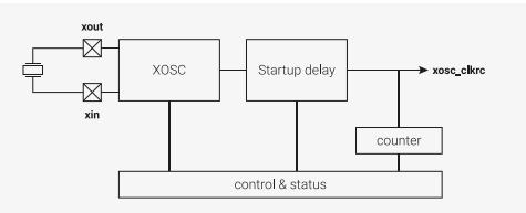
graph LR
    Crystal[Crystal] --- XIN[XIN]
    XOSC[XOSC] --- XOUT[XOUT]
    XOSC --- Startup[Startup delay]
    Startup --- Counter[counter]
    Counter --> xosc_clkrc[xosc_clkrc]
    CS[control & status] --- XOSC
CS --- Counter2.16.1.1. Recommended Crystals
For the best performance and stability across typical operating temperature ranges, it is recommended to use the Abracon ABM8-272-T3. You can source the ABM8-272-T3 directly from Abracon or from an authorised reseller. The Abracon ABM8-272-T3 has the following specifications:
Table 257. Key Crystal Specifications.
| Parameters | Minimum | Typical | Maximum | Units | Notes |
|---|---|---|---|---|---|
| Center Frequency | 12.000 | 12.000 | 12.000 | MHz | |
| Operation Mode | Fundamental-AT | Fundamental-AT | Fundamental-AT | ||
| Operating Temperature | -40 | +85 | °C | ||
| Storage Temperature | -55 | +125 | °C | ||
| Frequency Tolerance (25°C) | -30 | +30 | ppm | ||
| Frequency Stability (25°C) | -30 | +30 | ppm | ||
| Equivalent Series Resistance (R1) | 50 | Ω | |||
| Shunt Capacitance (C0) | 3.0 | pF | |||
| Load Capacitance (CL) | 10 | 10 | 10 | pF | |
| Drive Level | 10 | 200 | μW | ||
| Aging | -5 | +5 | ppm | @25±3°C, 1st year |
| Parameters | Minimum | Typical | Maximum | Units | Notes |
|---|---|---|---|---|---|
| Insulation Resistance | 500 | MΩ | @100Vdc±15V |
Even if you use a crystal with similar specifications, you will need to test the circuit over a range of temperatures to ensure stability.
The crystal oscillator is powered from the VDDIO voltage. As a result, the Abracon crystal and that particular damping resistor are tuned for 3.3V operation. If you use a different IO voltage, you will need to re-tune.
Any changes to crystal parameters risk instability across any components connected to the crystal circuit.
If you can't source the recommended crystal directly from Abracon or a reseller, contact applications@raspberrypi.com .
Raspberry Pi Pico has been specifically tuned for the specifications of the Abracon ABM8-272-T3 crystal. For an example of how to use a crystal with RP2040, see the Raspberry Pi Pico board schematic in Appendix B of the Raspberry Pi Pico Datasheet and the Raspberry Pi Pico design files .
2.16.2. Usage
The XOSC is disabled on chip startup and the RP2040 boots using the Ring Oscillator (ROSC). To start the XOSC, the programmer must set the CTRL_ENABLE register. The XOSC is not immediately usable because it takes time for the oscillations to build to sufficient amplitude. This time will be dependent on the chosen crystal but will be of the order of a few milliseconds. The XOSC incorporates a timer controlled by the STARTUP_DELAY register for automatically managing this and setting a flag (STATUS_STABLE) when the XOSC clock is usable.
2.16.3. Startup Delay
The STARTUP_DELAY register specifies how many clock cycles must be seen from the crystal before it can be used. This is specified in multiples of 256. The SDK
xosc_init
function sets this value. The 1ms default is sufficient for the RP2040 reference design (see the Minimal Design Example in
Hardware design with RP2040
) which runs the XOSC at 12MHz. When the timer expires, the STATUS_STABLE flag will be set to indicate the XOSC output can be used.
Before starting the XOSC the programmer must ensure the STARTUP_DELAY register is correctly configured. The required value can be calculated by:
So with a 12MHz crystal and a 1ms wait time, the calculation is:
NOTE
The value is rounded up to the nearest integer so the wait time will be just over 1ms
2.16.4. XOSC Counter
The COUNT register provides a method of managing short software delays. Writing a value to the COUNT register automatically triggers it to start counting down to zero at the XOSC frequency. The programmer then simply polls the register until it reaches zero. This is preferable to using NOPs in software loops because it is independent of the core clock frequency, the compiler and the execution time of the compiled code.
2.16.5. DORMANT mode
In DORMANT mode (see Section 2.11.3 ) all of the on-chip clocks can be paused to save power. This is particularly useful in battery-powered applications. The RP2040 is woken from DORMANT mode by an interrupt either from an external event such as an edge on a GPIO pin or from the on-chip RTC. This must be configured before entering DORMANT mode. If the RTC is being used to trigger wake-up then it must be clocked from an external source. To enter DORMANT mode the programmer must then switch all internal clocks to be driven from XOSC or ROSC and stop the PLLs. Then a specific 32-bit value must be written to the DORMANT register in the chosen oscillator (XOSC or ROSC) to stop it oscillating. When exiting DORMANT mode the chosen oscillator will restart. If XOSC is chosen then the frequency will be more precise but the restart time is longer due to the startup delay (>1ms on the RP2040 reference design (see the Minimal Design Example in Hardware design with RP2040 )). If ROSC is chosen then the frequency is less precise but the start-up time is very short (approximately 1µs).
 NOTE
NOTE
The PLLs must be stopped before entering DORMANT mode
SDK: https://github.com/raspberrypi/pico-sdk/blob/master/src/rp2_common/hardware_xosc/xosc.c Lines 56 - 63
56 void xosc_dormant(void) {
57 // WARNING: This stops the xosc until woken up by an irq
58 xosc_hw->dormant = XOSC_DORMANT_VALUE_DORMANT;
59 // Wait for it to become stable once woken up
60 while(!(xosc_hw->status & XOSC_STATUS_STABLE_BITS)) {
61 tight_loop_contents();
62 }
63 } WARNING
If no IRQ is configured before going into DORMANT mode the XOSC or ROSC will never restart.
See Section 2.11.5.2 for a complete example of DORMANT mode using the XOSC.
2.16.6. Programmer's Model
SDK: https://github.com/raspberrypi/pico-sdk/blob/master/src/rp2040/hardware_structs/include/hardware/structs/xosc.h Lines 27 - 59
27 typedef struct {
28     _REG_(XOSC_CTRL_OFFSET) // XOSC_CTRL
29     // Crystal Oscillator Control
30     // 0x00fff000 [23:12] ENABLE      (-) On power-up this field is initialised to DISABLE and
the...
31     // 0x0000fff [11:0]  FREQ_RANGE  (-) Frequency range
32     io_rw_32 ctrl;
33
34     _REG_(XOSC_STATUS_OFFSET) // XOSC_STATUS
35     // Crystal Oscillator Status
36     // 0x8000000 [31]    STABLE      (0) Oscillator is running and stable
37     // 0x0100000 [24]    BADWRITE    (0) An invalid value has been written to CTRL_ENABLE
or...
38     // 0x0001000 [12]    ENABLED     (-) Oscillator is enabled but not necessarily running
and...
39     // 0x0000003 [1:0]   FREQ_RANGE  (-) The current frequency range setting, always reads 0
40     io_rw_32 status;
41 }
42 _REG_(XOSC_DORMANT_OFFSET) // XOSC_DORMANT 43 // Crystal Oscillator pause control 44 // 0xffffffff [31:0] DORMANT (-) This is used to save power by pausing the XOSC + 45 io_rw_32 dormant; 46 47 _REG_(XOSC_STARTUP_OFFSET) // XOSC_STARTUP 48 // Controls the startup delay 49 // 0x00100000 [20] X4 (-) Multiplies the startup_delay by 4 50 // 0x00003fff [13:0] DELAY (-) in multiples of 256*xtal_period 51 io_rw_32 startup; 52 53 uint32_t _pad0[3]; 54 55 _REG_(XOSC_COUNT_OFFSET) // XOSC_COUNT 56 // A down counter running at the XOSC frequency which counts to zero and stops. 57 // 0x000000ff [7:0] COUNT (0x00) 58 io_rw_32 count; 59 } xosc_hw_t;
SDK: https://github.com/raspberrypi/pico-sdk/blob/master/src/rp2_common/hardware_xosc/xosc.c Lines 29 - 43
29 void xosc_init(void) {
30     // Assumes 1-15 MHz input, checked above.
31     xosc_hw->ctrl = XOSC_CTRL_FREQ_RANGE_VALUE_1_15MHZ;
32
33     // Set xosc startup delay
34     xosc_hw->startup = STARTUP_DELAY;
35
36     // Set the enable bit now that we have set freq range and startup delay
37     hw_set_bits(&xosc_hw->ctrl, XOSC_CTRL_ENABLE_VALUE_ENABLE << XOSC_CTRL_ENABLE_LSB);
38
39     // Wait for XOSC to be stable
40     while(!(xosc_hw->status & XOSC_STATUS_STABLE_BITS)) {
41         tight_loop_contents();
42     }
43 }
2.16.7. List of Registers
The XOSC registers start at a base address of 0x40024000 (defined as XOSC_BASE in SDK).
Table 258. List of XOSC registers
| Offset | Name | Info |
|---|---|---|
| 0x00 | CTRL | Crystal Oscillator Control |
| 0x04 | STATUS | Crystal Oscillator Status |
| 0x08 | DORMANT | Crystal Oscillator pause control |
| 0x0c | STARTUP | Controls the startup delay |
| 0x1c | COUNT | A down counter running at the XOSC frequency which counts to zero and stops. |
XOSC: CTRL Register
Offset: 0x00
DescriptionCrystal Oscillator Control
Table 259. CTRL Register
| Bits | Description | Type | Reset |
|---|---|---|---|
| 31:24 | Reserved. | - | - |
| 23:12 | ENABLE:
On power-up this field is initialised to DISABLE and the chip runs from the ROSC. If the chip has subsequently been programmed to run from the XOSC then setting this field to DISABLE may lock-up the chip. If this is a concern then run the clk_ref from the ROSC and enable the clk_sys RESUS feature. The 12-bit code is intended to give some protection against accidental writes. An invalid setting will enable the oscillator. | RW | - |
| Enumerated values: | |||
| 0xd1e → DISABLE | |||
| 0xfab → ENABLE | |||
| 11:0 | FREQ_RANGE: Frequency range. This resets to 0xAA0 and cannot be changed. | RW | - |
| Enumerated values: | |||
| 0xaa0 → 1_15MHZ | |||
| 0xaa1 → RESERVED_1 | |||
| 0xaa2 → RESERVED_2 | |||
| 0xaa3 → RESERVED_3 |
Offset: 0x04
DescriptionCrystal Oscillator Status
Table 260. STATUS Register
| Bits | Description | Type | Reset |
|---|---|---|---|
| 31 | STABLE: Oscillator is running and stable | RO | 0x0 |
| 30:25 | Reserved. | - | - |
| 24 | BADWRITE: An invalid value has been written to CTRL_ENABLE or CTRL_FREQ_RANGE or DORMANT | WC | 0x0 |
| 23:13 | Reserved. | - | - |
| 12 | ENABLED: Oscillator is enabled but not necessarily running and stable, resets to 0 | RO | - |
| 11:2 | Reserved. | - | - |
| 1:0 | FREQ_RANGE: The current frequency range setting, always reads 0 | RO | - |
| Enumerated values: | |||
| 0x0 → 1_15MHZ | |||
| 0x1 → RESERVED_1 | |||
| 0x2 → RESERVED_2 | |||
| 0x3 → RESERVED_3 |
XOSC: DORMANT Register
Offset: 0x08
Description
Crystal Oscillator pause control
Table 261. DORMANT Register
| Bits | Description | Type | Reset |
|---|---|---|---|
| 31:0 | This is used to save power by pausing the XOSC On power-up this field is initialised to WAKE An invalid write will also select WAKE WARNING: stop the PLLs before selecting dormant mode WARNING: setup the irq before selecting dormant mode | RW | - |
| Enumerated values: | |||
| 0x63f6d61 → DORMANT | |||
| 0x77616b65 → WAKE |
XOSC: STARTUP Register
Offset: 0x0c
Description
Controls the startup delay
Table 262. STARTUP Register
| Bits | Description | Type | Reset |
|---|---|---|---|
| 31:21 | Reserved. | - | - |
| 20 | X4 : Multiplies the startup_delay by 4. This is of little value to the user given that the delay can be programmed directly. | RW | 0x0 |
| 19:14 | Reserved. | - | - |
| 13:0 | DELAY : in multiples of 256*xtal_period. The reset value of 0xc4 corresponds to approx 50 000 cycles. | RW | 0x00c4 |
XOSC: COUNT Register
Offset: 0x1c
Table 263. COUNT Register
| Bits | Description | Type | Reset |
|---|---|---|---|
| 31:8 | Reserved. | - | - |
| 7:0 | A down counter running at the xosc frequency which counts to zero and stops. To start the counter write a non-zero value. Can be used for short software pauses when setting up time sensitive hardware. | RW | 0x00 |
2.17. Ring Oscillator (ROSC)
2.17.1. Overview
The Ring Oscillator (ROSC) is an on-chip oscillator built from a ring of inverters. It requires no external components and is started automatically during RP2040 power up. It provides the clock to the cores during boot. The frequency of the
ROSC is programmable and it can directly provide a high speed clock to the cores, but the frequency varies with Process, Voltage and Temperature (PVT) so it cannot provide clocks for components which require an accurate frequency such as the RTC, USB and ADC. Methods for mitigating the frequency variation are discussed in Section 2.15 but these are only relevant to very low power design. For most applications requiring accurate clock frequencies it is recommended to switch to the XOSC and PLLs. During boot the ROSC runs at a nominal 6.5MHz and is guaranteed to be in the range 1.8MHz to 12MHz.
Once the chip has booted the programmer can choose to continue running from the ROSC and increase its frequency or start the Crystal Oscillator (XOSC) and PLLs. The ROSC can be disabled after the system clocks have been switched to the XOSC. Each oscillator has advantages and the programmer can switch between them to achieve the best solution for the application.
Figure 34. ROSC overview.
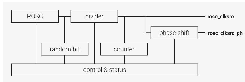
graph TD
    ROSC[ROSC] --- divider[divider]
    divider --- random_bit[random bit]
    divider --- counter[counter]
    random_bit --- counter
    counter --- phase_shift[phase shift]
    phase_shift --- divider
    divider --- rosc_clksrc[rosc_clksrc]
    divider --- rosc_clksrc_ph[rosc_clksrc_ph]
    control_status[control & status]
    ROSC --- control_status
    divider --- control_status
    random_bit --- control_status
    counter --- control_status
    phase_shift --- control_status
2.17.2. ROSC/XOSC trade-offs
The advantages of the ROSC are its flexibility and its low power. Also, there is no requirement for internal or external components when using the ROSC to provide clocks. Its frequency is programmable so it can be used to provide a fast core clock without starting the PLLs and can be divided by clock generators ( Section 2.15 ) to generate slower peripheral clocks. The ROSC starts immediately and responds immediately to the frequency controls. It will retain the frequency setting when entering and exiting the DORMANT state (see Section 2.11.3 ). However, the user must be aware that the frequency may have drifted when exiting the DORMANT state due to changes in the supply voltage and the chip temperature.
The disadvantage of the ROSC is its frequency variation with PVT (Process, Voltage & Temperature) which makes it unsuitable for generating precise clocks or for applications where software execution timing is important. However, the PVT frequency variation can be exploited to provide automatic frequency scaling to maximise performance. This is discussed in Section 2.15 .
The only advantage of the XOSC is its accurate frequency, but this is an overriding requirement in many applications.
The disadvantages of the XOSC are its requirement for external components (a crystal etc), its higher power consumption, slow startup time (>1ms) and fixed, low frequency. PLLs are required to produce higher frequency clocks. They consume more power and take significant time to start up and to change frequency. Exiting DORMANT mode is much slower than for ROSC because the XOSC must be restarted and the PLLs must be reconfigured.
2.17.3. Modifying the frequency
The ROSC is arranged as 8 stages, each with programmable drive. There are 2 methods of controlling the frequency. The frequency range controls the number of stages in the ROSC loop and the FREQA & FREQB registers control the drive strength of the stages.
The frequency range is changed by writing to the
FREQ_RANGE
register which controls the number of stages in the ROSC loop. The default LOW range has 8 (stages 0-7), MEDIUM has 6 (stages 2-7), HIGH has 4 (stages 4-7) and TOOHIGH has 2 (stages 6-7). It is recommended to change
FREQ_RANGE
one step at a time until the desired range is reached. The ROSC output will not glitch when increasing the frequency range, so the output clock can continue to be used. However, that is not true when going back down the frequency range. An alternate clock source must be selected for the modules clocked by ROSC, or they must be held in reset during the transition. The behaviour has not been fully characterised but the MEDIUM range will be approximately 1.33 times the LOW RANGE, the HIGH range will be 2 times
the LOW range and the TOOHIGH range will be 4 times the LOW range. The TOOHIGH range is aptly named. It should not be used because the internal logic of the ROSC will not run at that frequency.
The FREQA & FREQB registers control the drive strength of the stages in the ROSC loop. Increasing the drive strength reduces the delay through the stage and increases the oscillation frequency. Each stage has 3 drive strength control bits. Each bit turns on additional drive, therefore each stage has 4 drive strength settings equal to the number of bits set, with 0 being the default, 1 being double drive, 2 being triple drive and 3 being quadruple drive. Turning on extra drive will not have a linear effect on frequency, setting a second bit will have less impact than setting the first bit and so on. To ensure smooth transitions it is recommended to change one drive strength bit at a time. When
FREQ_RANGE
is used to shorten the ROSC loop, the bypassed stages still propagate the signal and therefore their drive strengths must be set to at least the same level as the lowest drive strength in the stages that are in the loop. This will not affect the oscillation frequency.
2.17.4. ROSC divider
The ROSC frequency is too fast to be used directly so is divided in an integer divider controlled by the DIV register. DIV can be changed while the ROSC is running, the output clock will change frequency without glitching. The default divisor is 16 which ensures the output clock is in the range 1.8 to 12MHz on chip startup.
The divider has 2 outputs,
rosc_clksrc
and
rosc_clksrc_ph
, the second being a phase shifted version of the first. This is primarily intended for use during product development and the outputs will be identical if the PHASE register is left in its default state.
2.17.5. Random Number Generator
If the system clocks are running from the XOSC and/or PLLs the ROSC can be used to generate random numbers. Simply enable the ROSC and read the
RANDBIT
register to get a 1-bit random number and read it
n
times to get an
n
-bit value. This does not meet the requirements of randomness for security systems because it can be compromised, but it may be useful in less critical applications. If the cores are running from the ROSC then the value will not be random because the timing of the register read will be correlated to the phase of the ROSC.
2.17.6. ROSC Counter
The
COUNT
register provides a method of managing short software delays. Writing a value to the
COUNT
register automatically triggers it to start counting down to zero at the ROSC frequency. The programmer then simply polls the register until it reaches zero. This is preferable to using NOPs in software loops because it is independent of the core clock frequency, the compiler and the execution time of the compiled code.
2.17.7. DORMANT mode
In DORMANT mode (see Section 2.11.3 ) all of the on-chip clocks can be paused to save power. This is particularly useful in battery-powered applications. The RP2040 is woken from DORMANT mode by an interrupt either from an external event such as an edge on a GPIO pin or from the on-chip RTC. This must be configured before entering DORMANT mode. If the RTC is being used to trigger wake-up then it must be clocked from an external source. To enter DORMANT mode the programmer must then switch all internal clocks to be driven from XOSC or ROSC and stop the PLLs. Then a specific 32-bit value must be written to the DORMANT register in the chosen oscillator (XOSC or ROSC) to stop it oscillating. When exiting DORMANT mode the chosen oscillator will restart. If XOSC is chosen then the frequency will be more precise but the restart time is longer due to the startup delay (>1ms on the RP2040 reference design (see the Minimal Design Example in Hardware design with RP2040 )). If ROSC is chosen then the frequency is less precise but the start-up time is very short (approximately 1µs).
Pico Extras: https://github.com/raspberrypi/pico-extras/blob/master/src/rp2_common/hardware_rosc/rosc.c Lines 56 - 61
56 void rosc_set_dormant(void) {
57     // WARNING: This stops the rosc until woken up by an irq
58     rosc_write(&rosc_hw->dormant, ROSC_DORMANT_VALUE_DORMANT);
59     // Wait for it to become stable once woken up
60     while(!(rosc_hw->status & ROSC_STATUS_STABLE_BITS));
61 }
WARNING
If no IRQ is configured before going into dormant mode the ROSC will never restart.
See Section 2.11.5.2 for some examples of dormant mode.
2.17.8. List of Registers
The ROSC registers start at a base address of
0x40060000
(defined as
ROSC_BASE
in SDK).
Table 264. List of ROSC registers
| Offset | Name | Info |
|---|---|---|
| 0x00 | CTRL | Ring Oscillator control |
| 0x04 | FREQA | Ring Oscillator frequency control A |
| 0x08 | FREQB | Ring Oscillator frequency control B |
| 0x0c | DORMANT | Ring Oscillator pause control |
| 0x10 | DIV | Controls the output divider |
| 0x14 | PHASE | Controls the phase shifted output |
| 0x18 | STATUS | Ring Oscillator Status |
| 0x1c | RANDOMBIT | Returns a 1 bit random value |
| 0x20 | COUNT | A down counter running at the ROSC frequency which counts to zero and stops. |
ROSC: CTRL Register
Offset: 0x00
Description
Ring Oscillator control
Table 265. CTRL Register
| Bits | Description | Type | Reset |
|---|---|---|---|
| 31:24 | Reserved. | - | - |
| 23:12 | ENABLE:
On power-up this field is initialised to ENABLE The system clock must be switched to another source before setting this field to DISABLE otherwise the chip will lock up The 12-bit code is intended to give some protection against accidental writes. An invalid setting will enable the oscillator. | RW | - |
| Enumerated values: | |||
| 0xd1e → DISABLE | |||
| 0xfab → ENABLE |
| Bits | Description | Type | Reset |
|---|---|---|---|
| 11:0 | FREQ_RANGE
: Controls the number of delay stages in the ROSC ring LOW uses stages 0 to 7 MEDIUM uses stages 2 to 7 HIGH uses stages 4 to 7 TOOHIGH uses stages 6 to 7 and should not be used because its frequency exceeds design specifications The clock output will not glitch when changing the range up one step at a time The clock output will glitch when changing the range down Note: the values here are gray coded which is why HIGH comes before TOOHIGH | RW | 0xaa0 |
| Enumerated values: | |||
| 0xfa4 → LOW | |||
| 0xfa5 → MEDIUM | |||
| 0xfa7 → HIGH | |||
| 0xfa6 → TOOHIGH |
ROSC: FREQA Register
Offset: 0x04
Description
The FREQA & FREQB registers control the frequency by controlling the drive strength of each stage
The drive strength has 4 levels determined by the number of bits set
Increasing the number of bits set increases the drive strength and increases the oscillation frequency
0 bits set is the default drive strength
1 bit set doubles the drive strength
2 bits set triples drive strength
3 bits set quadruples drive strength
Table 266. FREQA Register
| Bits | Description | Type | Reset |
|---|---|---|---|
| 31:16 | PASSWD
: Set to 0x9696 to apply the settings Any other value in this field will set all drive strengths to 0 | RW | 0x0000 |
| Enumerated values: | |||
| 0x9696 → PASS | |||
| 15 | Reserved. | - | - |
| 14:12 | DS3 : Stage 3 drive strength | RW | 0x0 |
| 11 | Reserved. | - | - |
| 10:8 | DS2 : Stage 2 drive strength | RW | 0x0 |
| 7 | Reserved. | - | - |
| 6:4 | DS1 : Stage 1 drive strength | RW | 0x0 |
| 3 | Reserved. | - | - |
| 2:0 | DS0 : Stage 0 drive strength | RW | 0x0 |
ROSC: FREQB Register
Offset: 0x08
Description
For a detailed description see freqa register
Table 267. FREQB Register
| Bits | Description | Type | Reset |
|---|---|---|---|
| 31:16 | PASSWD
: Set to 0x9696 to apply the settings Any other value in this field will set all drive strengths to 0 | RW | 0x0000 |
| Enumerated values: | |||
| 0x9696 → PASS | |||
| 15 | Reserved. | - | - |
| 14:12 | DS7 : Stage 7 drive strength | RW | 0x0 |
| 11 | Reserved. | - | - |
| 10:8 | DS6 : Stage 6 drive strength | RW | 0x0 |
| 7 | Reserved. | - | - |
| 6:4 | DS5 : Stage 5 drive strength | RW | 0x0 |
| 3 | Reserved. | - | - |
| 2:0 | DS4 : Stage 4 drive strength | RW | 0x0 |
ROSC: DORMANT Register
Offset: 0x0c
Description
Ring Oscillator pause control
Table 268. DORMANT Register
| Bits | Description | Type | Reset |
|---|---|---|---|
| 31:0 | This is used to save power by pausing the ROSC On power-up this field is initialised to WAKE An invalid write will also select WAKE Warning: setup the irq before selecting dormant mode | RW | - |
| Enumerated values: | |||
| 0x636f6d61 → DORMANT | |||
| 0x77616b65 → WAKE |
ROSC: DIV Register
Offset: 0x10
Description
Controls the output divider
Table 269. DIV Register
| Bits | Description | Type | Reset |
|---|---|---|---|
| 31:12 | Reserved. | - | - |
| 11:0 | set to 0xaa0 + div where div = 0 divides by 32 div = 1-31 divides by div any other value sets div=31 this register resets to div=16 | RW | - |
| Enumerated values: |
| Bits | Description | Type | Reset |
|---|---|---|---|
| 0xaa0 → PASS |
ROSC: PHASE Register
Offset: 0x14
Description
Controls the phase shifted output
Table 270. PHASE Register
| Bits | Description | Type | Reset |
|---|---|---|---|
| 31:12 | Reserved. | - | - |
| 11:4 | PASSWD
: set to 0xaa any other value enables the output with shift=0 | RW | 0x00 |
| 3 | ENABLE
: enable the phase-shifted output this can be changed on-the-fly | RW | 0x1 |
| 2 | FLIP
: invert the phase-shifted output this is ignored when div=1 | RW | 0x0 |
| 1:0 | SHIFT
: phase shift the phase-shifted output by SHIFT input clocks this can be changed on-the-fly must be set to 0 before setting div=1 | RW | 0x0 |
ROSC: STATUS Register
Offset: 0x18
Description
Ring Oscillator Status
Table 271. STATUS Register
| Bits | Description | Type | Reset |
|---|---|---|---|
| 31 | STABLE : Oscillator is running and stable | RO | 0x0 |
| 30:25 | Reserved. | - | - |
| 24 | BADWRITE : An invalid value has been written to CTRL_ENABLE or CTRL_FREQ_RANGE or FREQA or FREQB or DIV or PHASE or DORMANT | WC | 0x0 |
| 23:17 | Reserved. | - | - |
| 16 | DIV_RUNNING
: post-divider is running this resets to 0 but transitions to 1 during chip startup | RO | - |
| 15:13 | Reserved. | - | - |
| 12 | ENABLED
: Oscillator is enabled but not necessarily running and stable this resets to 0 but transitions to 1 during chip startup | RO | - |
| 11:0 | Reserved. | - | - |
ROSC: RANDOMBIT Register
Offset: 0x1c
Table 272. RANDOMBIT Register
| Bits | Description | Type | Reset |
|---|---|---|---|
| 31:1 | Reserved. | - | - |
| Bits | Description | Type | Reset |
|---|---|---|---|
| 0 | This just reads the state of the oscillator output so randomness is compromised if the ring oscillator is stopped or run at a harmonic of the bus frequency | RO | 0x1 |
ROSC: COUNT Register
Offset: 0x20
Table 273. COUNT Register
| Bits | Description | Type | Reset |
|---|---|---|---|
| 31:8 | Reserved. | - | - |
| 7:0 | A down counter running at the ROSC frequency which counts to zero and stops. To start the counter write a non-zero value. Can be used for short software pauses when setting up time sensitive hardware. | RW | 0x00 |
2.18. PLL
2.18.1. Overview
The PLL is designed to take a reference clock, and multiply it using a VCO (Voltage Controlled Oscillator) with a feedback loop. The VCO must run at high frequencies (between 750 and 1600MHz), so there are two dividers, known as post dividers that can divide the VCO frequency before it is distributed to the clock generators on the chip.
There are two PLLs in RP2040. They are:
- • pll_sys - Used to generate up to a 133MHz system clock
- • pll_usb - Used to generate a 48MHz USB reference clock
Figure 35. On both PLLs, the FREF (reference) input is connected to the crystal oscillator's XI input. The PLL contains a VCO, which is locked to a constant ratio of the reference clock via the feedback loop (phase-frequency detector and loop filter). This can synthesise very high frequencies, which may be divided down by the post-dividers.
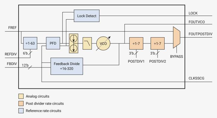
2.18.2. Calculating PLL parameters
To configure the PLL, you must know the frequency of the reference clock, which on RP2040 is routed directly from the crystal oscillator. This will often be a 12MHz crystal, for compatibility with RP2040's USB bootrom. The PLL's final output frequency FOUTPOSTDIV can then be calculated as \( (FREF / REFDIV) \times FBDIV / (POSTDIV1 \times POSTDIV2) \) . With a desired output frequency in mind, you must select PLL parameters according to the following constraints of the PLL design:
- • Minimum reference frequency (FREF / REFDIV) is 5MHz
- • Oscillator frequency ( \( F_{OUTVCO} \) ) must be in the range 750MHz \( \rightarrow \) 1600MHz
- • Feedback divider ( \( FBDIV \) ) must be in the range 16 \( \rightarrow \) 320
- • The post dividers \( POSTDIV1 \) and \( POSTDIV2 \) must be in the range 1 \( \rightarrow \) 7
- • Maximum input frequency ( \( F_{REF} / REFDIV \) ) is VCO frequency divided by 16, due to minimum feedback divisor
Additionally, the maximum frequencies of the chip's clock generators (attached to \( F_{OUTPOSTDIV} \) ) must be respected. For the system PLL this is 133MHz, and for the USB PLL, 48MHz.
 NOTE
NOTE
The crystal oscillator on RP2040 is designed for crystals between 5 and 15MHz, so typically \( REFDIV \) should be 1. If the application circuit drives a faster reference directly into the XI input, and a low VCO frequency is desired, the reference divisor can be increased to keep the PLL input within a suitable range.
 TIP
TIP
When two different values are required for \( POSTDIV1 \) and \( POSTDIV2 \) , it's preferable to assign the higher value to \( POSTDIV1 \) , for lower power consumption.
In the RP2040 reference design (see the Minimal Design Example in Hardware design with RP2040 ), which attaches a 12MHz crystal to the crystal oscillator, this implies that the minimum achievable and legal VCO frequency is \( 12\text{MHz} \times 63 = 756\text{MHz} \) , and the maximum VCO is \( 12\text{MHz} \times 133 = 1596\text{MHz} \) , so \( FBDIV \) must remain in the range 63 \( \rightarrow \) 133. For example, setting \( FBDIV \) to 100 would synthesise a 1200MHz VCO frequency. A \( POSTDIV1 \) value of 6 and a \( POSTDIV2 \) value of 2 would divide this by 12 in total, producing a clean 100MHz at the PLL's final output.
2.18.2.1. Jitter vs Power Consumption
There are often several sets of PLL configuration parameters which achieve, or are very close to, the desired output frequency. It is up to the programmer to decide whether to prioritise low PLL power consumption, or lower jitter , which is cycle-to-cycle variation in the PLL's output clock period. This is not a concern as far as system stability is concerned, because RP2040's digital logic is designed with margin for the worst-case possible jitter on the system clock, but a highly accurate clock is often needed for audio and video applications, or where data is being transmitted and received in accordance with a specification. For example, the USB specification defines a maximum amount of allowable jitter.
Jitter is minimised by running the VCO at the highest possible frequency, so that higher post-divide values can be used. For example, \( 1500\text{MHz VCO} / 6 / 2 = 125\text{MHz} \) . To reduce power consumption, the VCO frequency should be as low as possible. For example: \( 750\text{MHz VCO} / 6 / 1 = 125\text{MHz} \) .
Another consideration here is that slightly adjusting the output frequency may allow a much lower VCO frequency to be achieved, by bringing the output to a closer rational multiple of the input. Indeed the exact desired frequency may not be exactly achievable with any allowable VCO frequency, or combination of divisors.
SDK provides a Python script that searches for the best VCO and post divider options for a desired output frequency:
SDK: https://github.com/raspberrypi/pico-sdk/blob/master/src/rp2-common/hardware_clocks/scripts/vccalc.py
1 #!/usr/bin/env python3
2
3 import argparse
4 import sys
5
6 # Fixed hardware parameters
7 fbdiv_range = range(16, 320 + 1)
8 postdiv_range = range(1, 7 + 1)
9 ref_min = 5
10 refdiv_min = 1
11 refdiv_max = 63
12
13 def validRefdiv(string):
14     if ((int(string) < refdiv_min) or (int(string) > refdiv_max)):
15         raise ValueError("REFDIV must be in the range {} to {}".format(refdiv_min,
16                                 refdiv_max))
17     return int(string)
18
19 parser = argparse.ArgumentParser(description="PLL parameter calculator")
20 parser.add_argument("--input", "-i", default=12, help="Input (reference) frequency. Default
21     12 MHz", type=float)
22 parser.add_argument("--ref-min", default=5, help="Override minimum reference frequency.
23     Default 5 MHz", type=float)
24 parser.add_argument("--vco-max", default=1600, help="Override maximum VCO frequency. Default
25     1600 MHz", type=float)
26 parser.add_argument("--vco-min", default=750, help="Override minimum VCO frequency. Default
27     750 MHz", type=float)
28 parser.add_argument("--cmake", action="store_true", help="Print out a CMake snippet to apply
29     the selected PLL parameters to your program")
30 parser.add_argument("--cmake-only", action="store_true", help="Same as --cmake, but do not
31     print anything other than the CMake output")
32 parser.add_argument("--cmake-executable-name", default="<program>", help="Set the executable
33     name to use in the generated CMake output")
34 parser.add_argument("--lock-refdiv", help="Lock REFDIV to specified number in the range {} to
35     {}".format(refdiv_min, refdiv_max), type=validRefdiv)
36 parser.add_argument("--low-vco", "-l", action="store_true", help="Use a lower VCO frequency
37     when possible. This reduces power consumption, at the cost of increased jitter")
38 parser.add_argument("output", help="Output frequency in MHz.", type=float)
39 args = parser.parse_args()
40
41 refdiv_range = range(refdiv_min, max(refdiv_min, min(refdiv_max, int(args.input / args
42     .ref_min))) + 1)
43 if args.lock_refdiv:
44     print("Locking REFDIV to", args.lock_refdiv)
45     refdiv_range = [args.lock_refdiv]
46
47 best = (0, 0, 0, 0, 0, 0)
48 best_margin = args.output
49
50 for refdiv in refdiv_range:
51     for fbdiv in fbdiv_range:
52         vco = args.input / refdiv * fbdiv
53         if vco < args.vco_min or vco > args.vco_max:
54             continue
55         # pd1 is inner loop so that we prefer higher ratios of pd1:pd2
56         for pd2 in postdiv_range:
57             for pd1 in postdiv_range:
58                 out = vco / pd1 / pd2
59                 margin = abs(out - args.output)
60                 vco_is_better = vco < best[5] if args.low_vco else vco > best[5]
61                 if ((vco * 1000) % (pd1 * pd2)):
62                     continue
63                 if margin < best_margin or (abs(margin - best_margin) < 1e-9 and
64                     vco_is_better):
65                     best = (out, fbdiv, pd1, pd2, refdiv, vco)
66                     best_margin = margin
67
68 best_out, best_fbdiv, best_pd1, best_pd2, best_refdiv, best_vco = best
69
70 if best[0] > 0:
71     cmake_output = \
72 f"""target_compile_definitions({args.cmake_executable_name} PRIVATE
73     PLL_SYS_REFDIV={best_refdiv}
74     PLL_SYS_VCO_FREQ_HZ={int((args.input * 1_000_000) / best_refdiv * best_fbdiv)}
75     PLL_SYS_POSTDIV1={best_pd1}
64     PLL_SYS_POSTDIV2={best_pd2}
65     SYS_CLK_HZ={int((args.input * 1_000_000) / (best_refdiv * best_pd1 * best_pd2) *
    best_fbdiv)}
66 )
67 """
68 if not args.cmake_only:
69     print("Requested: {} MHz".format(args.output))
70     print("Achieved: {} MHz".format(best_out))
71     print("REFDIV: {}".format(best_refdiv))
72     print("FBDIV: {} (VCO = {} MHz)".format(best_fbdiv, args.input / best_refdiv *
    best_fbdiv))
73     print("PD1: {}".format(best_pd1))
74     print("PD2: {}".format(best_pd2))
75     if best_refdiv != 1:
76         print(
77             "\nThis requires a non-default REFDIV value.\n"
78             "Add the following to your CMakeLists.txt to apply the REFDIV:\n"
79         )
80     elif args.cmake or args.cmake_only:
81         print("")
82     if args.cmake or args.cmake_only or best_refdiv != 1:
83         print(cmake_output)
84 else:
85     sys.exit("No solution found")
Given an input and output frequency, this script will find the best possible set of PLL parameters to get as close as possible. Where multiple equally good combinations are found, it returns the parameters which yield the highest VCO frequency, for best output stability. The
-l
or
--low-vco
flag will instead prefer lower frequencies, for reduced power consumption.
Here a 48MHz output is requested:
$ ./vcocalc.py 48
Requested: 48.0 MHz
Achieved: 48.0 MHz
FBDIV: 120 (VCO = 1440 MHz)
PD1: 6
PD2: 5
Asking for a 48MHz output with a lower VCO frequency, if possible:
$ ./vcocalc.py -l 48
Requested: 48.0 MHz
Achieved: 48.0 MHz
FBDIV: 64 (VCO = 768 MHz)
PD1: 4
PD2: 4
For a 125MHz system clock with a 12MHz input, the minimum VCO frequency is quite high.
$ ./vcocalc.py -l 125
Requested: 125.0 MHz
Achieved: 125.0 MHz
FBDIV: 125 (VCO = 1500 MHz)
PD1: 6
PD2: 2
We can restrict the search to lower VCO frequencies, so that the script will consider looser frequency matches. Note that, whilst a 750MHz VCO would be ideal here, we can't achieve exactly 750MHz by multiplying the 12MHz input by an integer, which is why the previous invocation returned such a high VCO frequency.
$ ./vcocalc.py -l 125 --vco-max 800
Requested: 125.0 MHz
Achieved: 126.0 MHz
FBDIV: 63 (VCO = 756 MHz)
PD1: 6
PD2: 1
A 126MHz system clock may be a tolerable deviation from the desired 125MHz, and generating this clock consumes less power at the PLL.
2.18.3. Configuration
The SDK uses the following PLL settings:
SDK: https://github.com/raspberrypi/pico-sdk/blob/master/src/rp2_common/hardware_clocks/include/hardware/clocks.h Lines 143 - 164
143 // There are two PLLs in RP-series microcontrollers:
144 // 1. The 'SYS PLL' generates the system clock, the frequency is defined by `SYS_CLK_KHZ`.
145 // 2. The 'USB PLL' generates the USB clock, the frequency is defined by `USB_CLK_KHZ`.
146 //
147 // The two PLLs use the crystal oscillator output directly as their reference frequency input;
148 // the PLLs reference
149 // frequency cannot be reduced by the dividers present in the clocks block. The crystal
150 // frequency is defined by `XOSC_HZ` (or
151 // `XOSC_KHZ` or `XOSC_MHZ`).
152 //
153 // The system's default definitions are correct for the above frequencies with a 12MHz
154 // crystal frequency. If different frequencies are required, these must be defined in
155 // the board configuration file together with the revised PLL settings
156 // Use `vcocalc.py` to check and calculate new PLL settings if you change any of these
157 // frequencies.
158 //
159 // Default PLL configuration RP2040:
160 //
161 // REF      FBDIV VCO      POSTDIV
162 // PLL SYS: 12 / 1 = 12MHz * 125 = 1500MHz / 6 / 2 = 125MHz
163 // PLL USB: 12 / 1 = 12MHz * 100 = 1200MHz / 5 / 5 = 48MHz
164 //
165 // Default PLL configuration RP2350:
166 //
167 // REF      FBDIV VCO      POSTDIV
168 // PLL SYS: 12 / 1 = 12MHz * 125 = 1500MHz / 5 / 2 = 150MHz
169 // PLL USB: 12 / 1 = 12MHz * 100 = 1200MHz / 5 / 5 = 48MHz
The
pll_init
function in the SDK, which we will examine below, asserts that all of these conditions are true before attempting to configure the PLL.
The SDK defines the PLL control registers as a struct. It then maps them into memory for each instance of the PLL.
SDK: https://github.com/raspberrypi/pico-sdk/blob/master/src/rp2040/hardware_structs/include/hardware/structs/pll.h Lines 27 - 53
27 typedef struct {
28     _REG_(PLL_CS_OFFSET) // PLL_CS
29     // Control and Status
30     // 0x00000000 [31] LOCK          (0) PLL is locked
31     // 0x00000100 [8]  BYPASS        (0) Passes the reference clock to the output instead of
    the...
32     // 0x0000003f [5:0] REFDIV        (0x01) Divides the PLL input reference clock
33     io_rw_32 cs;
34
35     _REG_(PLL_PWR_OFFSET) // PLL_PWR
36     // Controls the PLL power modes
37     // 0x00000020 [5]  VCOPD          (1) PLL VCO powerdown +
38     // 0x00000008 [3]  POSTDIVPD      (1) PLL post divider powerdown +
39     // 0x00000004 [2]  DSMPD          (1) PLL DSM powerdown +
40     // 0x00000001 [0]  PD              (1) PLL powerdown +
41     io_rw_32 pwr;
42
43     _REG_(PLL_FBDIV_INT_OFFSET) // PLL_FBDIV_INT
44     // Feedback divisor
45     // 0x00000fff [11:0] FBDIV_INT    (0x000) see ctrl reg description for constraints
46     io_rw_32 fbdiv_int;
47
48     _REG_(PLL_PRIM_OFFSET) // PLL_PRIM
49     // Controls the PLL post dividers for the primary output
50     // 0x00070000 [18:16] POSTDIV1     (0x7) divide by 1-7
51     // 0x00007000 [14:12] POSTDIV2     (0x7) divide by 1-7
52     io_rw_32 prim;
53 } pll_hw_t;
The SDK defines
pll_init
which is used to configure, or reconfigure a PLL. It starts by clearing any previous power state in the PLL, then calculates the appropriate feedback divider value. There are assertions to check these values satisfy the constraints above.
SDK: https://github.com/raspberrypi/pico-sdk/blob/master/src/rp2_common/hardware_pll/pll.c Lines 13 - 21
13 void pll_init(PLL pll, uint refdiv, uint vco_freq, uint post_div1, uint post_div2) {
14     uint32_t ref_freq = XOSC_HZ / refdiv;
15
16     // Check vco freq is in an acceptable range
17     assert(vco_freq >= PICO_PLL_VCO_MIN_FREQ_HZ && vco_freq <= PICO_PLL_VCO_MAX_FREQ_HZ);
18
19     // What are we multiplying the reference clock by to get the vco freq
20     // (The regs are called div, because you divide the vco output and compare it to the
    refclk)
21     uint32_t fbdiv = vco_freq / ref_freq;
The programming sequence for the PLL is as follows:
- • Program the reference clock divider (is a divide by 1 in the RP2040 case)
- • Program the feedback divider
- • Turn on the main power and VCO
- • Wait for the VCO to lock (i.e. keep its output frequency stable)
- • Set up post dividers and turn them on
SDK: https://github.com/raspberrypi/pico-sdk/blob/master/src/rp2-common/hardware_pll/pll.c Lines 42 - 69
42     if ((pll->cs & PLL_CS_LOCK_BITS) &&
43         (refdiv == (pll->cs & PLL_CS_REFDIV_BITS)) &&
44         (fbdiv == (pll->fbdiv_int & PLL_FBDIV_INT_BITS)) &&
45         (pdiv == (pll->prim & (PLL_PRIM_POSTDIV1_BITS | PLL_PRIM_POSTDIV2_BITS)))) {
46         // do not disrupt PLL that is already correctly configured and operating
47         return;
48     }
49
50     reset_unreset_block_num_wait_blocking(PLL_RESET_NUM(pll));
51
52     // Load VCO-related dividers before starting VCO
53     pll->cs = refdiv;
54     pll->fbdiv_int = fbdiv;
55
56     // Turn on PLL
57     uint32_t power = PLL_PWR_PD_BITS | // Main power
58                   PLL_PWR_VCO_PD_BITS; // VCO Power
59
60     hw_clear_bits(&pll->pwr, power);
61
62     // Wait for PLL to lock
63     while (!(pll->cs & PLL_CS_LOCK_BITS)) tight_loop_contents();
64
65     // Set up post dividers
66     pll->prim = pdiv;
67
68     // Turn on post divider
69     hw_clear_bits(&pll->pwr, PLL_PWR_POSTDIVPD_BITS);
Note the VCO is turned on first, followed by the post dividers so the PLL does not output a dirty clock while the VCO is locking.
2.18.4. List of Registers
The PLL_SYS and PLL_USB registers start at base addresses of
0x40028000
and
0x4002c000
respectively (defined as
PLL_SYS_BASE
and
PLL_USB_BASE
in SDK).
Table 274. List of PLL registers
| Offset | Name | Info |
|---|---|---|
| 0x0 | CS | Control and Status |
| 0x4 | PWR | Controls the PLL power modes. |
| 0x8 | FBDIV_INT | Feedback divisor |
| 0xc | PRIM | Controls the PLL post dividers for the primary output |
PLL: CS Register
Offset: 0x0
Description
Control and Status
GENERAL CONSTRAINTS:
Reference clock frequency min=5MHz, max=800MHz
Feedback divider min=16, max=320
VCO frequency min=750MHz, max=1600MHz
Table 275. CS Register
| Bits | Description | Type | Reset |
|---|---|---|---|
| 31 | LOCK : PLL is locked | RO | 0x0 |
| 30:9 | Reserved. | - | - |
| 8 | BYPASS : Passes the reference clock to the output instead of the divided VCO. The VCO continues to run so the user can switch between the reference clock and the divided VCO but the output will glitch when doing so. | RW | 0x0 |
| 7:6 | Reserved. | - | - |
| 5:0 | REFDIV
: Divides the PLL input reference clock. Behaviour is undefined for div=0. PLL output will be unpredictable during refdiv changes, wait for lock=1 before using it. | RW | 0x01 |
PLL: PWR Register
Offset: 0x4
Description
Controls the PLL power modes.
Table 276. PWR Register
| Bits | Description | Type | Reset |
|---|---|---|---|
| 31:6 | Reserved. | - | - |
| 5 | VCOPD
: PLL VCO powerdown To save power set high when PLL output not required or bypass=1. | RW | 0x1 |
| 4 | Reserved. | - | - |
| 3 | POSTDIVPD
: PLL post divider powerdown To save power set high when PLL output not required or bypass=1. | RW | 0x1 |
| 2 | DSMPD
: PLL DSM powerdown Nothing is achieved by setting this low. | RW | 0x1 |
| 1 | Reserved. | - | - |
| 0 | PD
: PLL powerdown To save power set high when PLL output not required. | RW | 0x1 |
PLL: FBDIV_INT Register
Offset: 0x8
Description
Feedback divisor
(note: this PLL does not support fractional division)
Table 277. FBDIV_INT Register
| Bits | Description | Type | Reset |
|---|---|---|---|
| 31:12 | Reserved. | - | - |
| 11:0 | see ctrl reg description for constraints | RW | 0x000 |
PLL: PRIM Register
Offset: 0xc
Description
Controls the PLL post dividers for the primary output
(note: this PLL does not have a secondary output)
the primary output is driven from VCO divided by postdiv1*postdiv2
Table 278. PRIM
Register
| Bits | Description | Type | Reset |
|---|---|---|---|
| 31:19 | Reserved. | - | - |
| 18:16 | POSTDIV1 : divide by 1-7 | RW | 0x7 |
| 15 | Reserved. | - | - |
| 14:12 | POSTDIV2 : divide by 1-7 | RW | 0x7 |
| 11:0 | Reserved. | - | - |
2.19. GPIO
2.19.1. Overview
RP2040 has 36 multi-functional General Purpose Input / Output (GPIO) pins, divided into two banks. In a typical use case, the pins in the QSPI bank (QSPI_SS, QSPI_SCLK and QSPI_SD0 to QSPI_SD3) are used to execute code from an external flash device, leaving the User bank (GPIO0 to GPIO29) for the programmer to use. All GPIOs support digital input and output, but GPIO26 to GPIO29 can also be used as inputs to the chip's Analogue to Digital Converter (ADC). Each GPIO can be controlled directly by software running on the processors, or by a number of other functional blocks.
The User GPIO bank supports the following functions:
- • Software control via SIO (Single-Cycle IO) - Section 2.3.1.2, "GPIO Control"
- • Programmable IO (PIO) - Chapter 3, PIO
- • 2 × SPI - Section 4.4, "SPI"
- • 2 × UART - Section 4.2, "UART"
- • 2 × I2C (two-wire serial interface) - Section 4.3, "I2C"
- • 8 × two-channel PWM - Section 4.5, "PWM"
- • 2 × external clock inputs - Section 2.15.2.3, "External Clocks"
- • 4 × general purpose clock output - Section 2.15, "Clocks"
- • 4 × input to ADC - Section 4.9, "ADC and Temperature Sensor"
- • USB VBUS management - Section 4.1.2.10, "VBUS Control"
- • External interrupt requests, level or edge-sensitive
The QSPI bank supports the following functions:
- • Software control via SIO (Single-Cycle IO) - Section 2.3.1.2, "GPIO Control"
- • Flash execute in place (XIP) - Section 2.6.3, "Flash"
The logical structure of an example IO is shown in Figure 36 .
Figure 36. Logical structure of a GPIO. Each GPIO can be controlled by one of a number of peripherals, or by software control registers in the SIO. The function select (FSEL) selects which peripheral output is in control of the GPIO's direction and output level, and/or which peripheral input can see this GPIO's input level. These three signals (output level, output enable, input level) can also be inverted, or forced high or low, using the GPIO control registers.
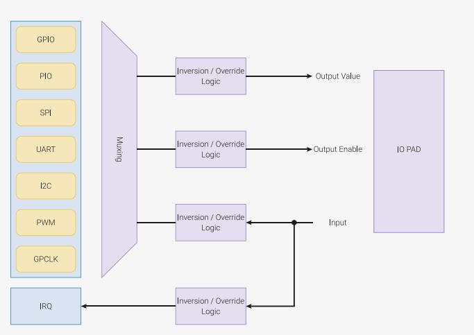
2.19.2. Function Select
The function allocated to each GPIO is selected by writing to the FUNCSEL field in the GPIO's CTRL register. See GPIO0_CTRL as an example. The functions available on each IO are shown in Table 279 and Table 281 .
Table 279. General Purpose Input/Output (GPIO) User Bank Functions
| Function | |||||||||
|---|---|---|---|---|---|---|---|---|---|
| GPIO | F1 | F2 | F3 | F4 | F5 | F6 | F7 | F8 | F9 |
| 0 | SPI0 RX | UART0 TX | I2C0 SDA | PWM0 A | SIO | PIO0 | PIO1 | USB OVCUR DET | |
| 1 | SPI0 CSn | UART0 RX | I2C0 SCL | PWM0 B | SIO | PIO0 | PIO1 | USB VBUS DET | |
| 2 | SPI0 SCK | UART0 CTS | I2C1 SDA | PWM1 A | SIO | PIO0 | PIO1 | USB VBUS EN | |
| 3 | SPI0 TX | UART0 RTS | I2C1 SCL | PWM1 B | SIO | PIO0 | PIO1 | USB OVCUR DET | |
| 4 | SPI0 RX | UART1 TX | I2C0 SDA | PWM2 A | SIO | PIO0 | PIO1 | USB VBUS DET | |
| 5 | SPI0 CSn | UART1 RX | I2C0 SCL | PWM2 B | SIO | PIO0 | PIO1 | USB VBUS EN | |
| 6 | SPI0 SCK | UART1 CTS | I2C1 SDA | PWM3 A | SIO | PIO0 | PIO1 | USB OVCUR DET | |
| 7 | SPI0 TX | UART1 RTS | I2C1 SCL | PWM3 B | SIO | PIO0 | PIO1 | USB VBUS DET | |
| 8 | SPI1 RX | UART1 TX | I2C0 SDA | PWM4 A | SIO | PIO0 | PIO1 | USB VBUS EN | |
| 9 | SPI1 CSn | UART1 RX | I2C0 SCL | PWM4 B | SIO | PIO0 | PIO1 | USB OVCUR DET | |
| 10 | SPI1 SCK | UART1 CTS | I2C1 SDA | PWM5 A | SIO | PIO0 | PIO1 | USB VBUS DET | |
| 11 | SPI1 TX | UART1 RTS | I2C1 SCL | PWM5 B | SIO | PIO0 | PIO1 | USB VBUS EN | |
| 12 | SPI1 RX | UART0 TX | I2C0 SDA | PWM6 A | SIO | PIO0 | PIO1 | USB OVCUR DET | |
| 13 | SPI1 CSn | UART0 RX | I2C0 SCL | PWM6 B | SIO | PIO0 | PIO1 | USB VBUS DET | |
| 14 | SPI1 SCK | UART0 CTS | I2C1 SDA | PWM7 A | SIO | PIO0 | PIO1 | USB VBUS EN | |
| 15 | SPI1 TX | UART0 RTS | I2C1 SCL | PWM7 B | SIO | PIO0 | PIO1 | USB OVCUR DET | |
| 16 | SPI0 RX | UART0 TX | I2C0 SDA | PWM0 A | SIO | PIO0 | PIO1 | USB VBUS DET | |
| 17 | SPI0 CSn | UART0 RX | I2C0 SCL | PWM0 B | SIO | PIO0 | PIO1 | USB VBUS EN | |
| 18 | SPI0 SCK | UART0 CTS | I2C1 SDA | PWM1 A | SIO | PIO0 | PIO1 | USB OVCUR DET | |
| 19 | SPI0 TX | UART0 RTS | I2C1 SCL | PWM1 B | SIO | PIO0 | PIO1 | USB VBUS DET | |
| 20 | SPI0 RX | UART1 TX | I2C0 SDA | PWM2 A | SIO | PIO0 | PIO1 | CLOCK GPIN0 | USB VBUS EN |
| Function | |||||||||
|---|---|---|---|---|---|---|---|---|---|
| 21 | SPI0 CSn | UART1 RX | I2C0 SCL | PWM2 B | SIO | PIO0 | PIO1 | CLOCK GPOUT0 | USB OVCUR DET |
| 22 | SPI0 SCK | UART1 CTS | I2C1 SDA | PWM3 A | SIO | PIO0 | PIO1 | CLOCK GPIN1 | USB VBUS DET |
| 23 | SPI0 TX | UART1 RTS | I2C1 SCL | PWM3 B | SIO | PIO0 | PIO1 | CLOCK GPOUT1 | USB VBUS EN |
| 24 | SPI1 RX | UART1 TX | I2C0 SDA | PWM4 A | SIO | PIO0 | PIO1 | CLOCK GPOUT2 | USB OVCUR DET |
| 25 | SPI1 CSn | UART1 RX | I2C0 SCL | PWM4 B | SIO | PIO0 | PIO1 | CLOCK GPOUT3 | USB VBUS DET |
| 26 | SPI1 SCK | UART1 CTS | I2C1 SDA | PWM5 A | SIO | PIO0 | PIO1 | USB VBUS EN | |
| 27 | SPI1 TX | UART1 RTS | I2C1 SCL | PWM5 B | SIO | PIO0 | PIO1 | USB OVCUR DET | |
| 28 | SPI1 RX | UART0 TX | I2C0 SDA | PWM6 A | SIO | PIO0 | PIO1 | USB VBUS DET | |
| 29 | SPI1 CSn | UART0 RX | I2C0 SCL | PWM6 B | SIO | PIO0 | PIO1 | USB VBUS EN | |
Each GPIO can have one function selected at a time. Likewise, each peripheral input (e.g. UART0 RX) should only be selected on one GPIO at a time. If the same peripheral input is connected to multiple GPIOs, the peripheral sees the logical OR of these GPIO inputs.
Table 280. GPIO User Bank function descriptions
| Function Name | Description |
|---|---|
| SPIx | Connect one of the internal PL022 SPI peripherals to GPIO |
| UARTx | Connect one of the internal PL011 UART peripherals to GPIO |
| I2Cx | Connect one of the internal DW I2C peripherals to GPIO |
| PWMx A/B | Connect a PWM slice to GPIO. There are eight PWM slices, each with two output channels (A/B). The B pin can also be used as an input, for frequency and duty cycle measurement. |
| SIO | Software control of GPIO, from the single-cycle IO (SIO) block. The SIO function (F5) must be selected for the processors to drive a GPIO, but the input is always connected, so software can check the state of GPIOs at any time. |
| PIOx | Connect one of the programmable IO blocks (PIO) to GPIO. PIO can implement a wide variety of interfaces, and has its own internal pin mapping hardware, allowing flexible placement of digital interfaces on user bank GPIOs. The PIO function (F6, F7) must be selected for PIO to drive a GPIO, but the input is always connected, so the PIOs can always see the state of all pins. |
| CLOCK GPINx | General purpose clock inputs. Can be routed to a number of internal clock domains on RP2040, e.g. to provide a 1Hz clock for the RTC, or can be connected to an internal frequency counter. |
| CLOCK GPOUTx | General purpose clock outputs. Can drive a number of internal clocks onto GPIOs, with optional integer divide. |
| USB OVCUR DET/VBUS DET/VBUS EN | USB power control signals to/from the internal USB controller |
Table 281. General Purpose Input/Output (GPIO) QSPI Bank Functions
| Function | ||||||||||
|---|---|---|---|---|---|---|---|---|---|---|
| IO | F0 | F1 | F2 | F3 | F4 | F5 | F6 | F7 | F8 | F9 |
| QSPI SCK | XIP SCK | SIO | ||||||||
| QSPI CSn | XIP CSn | SIO | ||||||||
| QSPI SD0 | XIP SD0 | SIO | ||||||||
| Function | ||||||||||
|---|---|---|---|---|---|---|---|---|---|---|
| QSPI SD1 | XIP SD1 | SIO | ||||||||
| QSPI SD2 | XIP SD2 | SIO | ||||||||
| QSPI SD3 | XIP SD3 | SIO | ||||||||
Table 282. GPIO QSPI Bank function descriptions
| Function Name | Description |
|---|---|
| XIP | Connection to the synchronous serial interface (SSI) inside the flash execute in place (XIP) subsystem. This allows processors to execute code directly from an external SPI, Dual-SPI or Quad-SPI flash |
| SIO | Software control of GPIO, from the single-cycle IO (SIO) block. The SIO function (F5) must be selected for the processors to
drive
a GPIO, but the input is always connected, so software can check the state of GPIOs at any time. The QSPI IOs are controlled via the
SIO_GPIO_HI_x
registers, and are mapped to register bits in the order SCK, CSn, SD0, SD1, SD2, SD3, starting at the LSB. |
The six QSPI Bank GPIO pins are typically used by the XIP peripheral to communicate with an external flash device. However, there are two scenarios where the pins can be used as software-controlled GPIOs:
- • If a SPI or Dual-SPI flash device is used for execute-in-place, then the SD2 and SD3 pins are not used for flash access, and can be used for other GPIO functions on the circuit board.
- • If RP2040 is used in a flashless configuration (USB boot only), then all six pins can be used for software-controlled GPIO functions
2.19.3. Interrupts
An interrupt can be generated for every GPIO pin in four scenarios:
- • Level High: the GPIO pin is a logical 1
- • Level Low: the GPIO pin is a logical 0
- • Edge High: the GPIO has transitioned from a logical 0 to a logical 1
- • Edge Low: the GPIO has transitioned from a logical 1 to a logical 0
The level interrupts are not latched. This means that if the pin is a logical 1 and the level high interrupt is active, it will become inactive as soon as the pin changes to a logical 0. The edge interrupts are stored in the
INTR
register and can be cleared by writing to the
INTR
register.
There are enable, status, and force registers for three interrupt destinations: proc 0, proc 1, and dormant_wake. For proc 0 the registers are enable (
PROC0_INTE0
), status (
PROC0_INTS0
), and force (
PROC0_INTF0
). Dormant wake is used to wake the ROSC or XOSC up from dormant mode. See
Section 2.11.5.2
for more information on dormant mode.
All interrupts are ORed together per-bank per-destination resulting in a total of six GPIO interrupts:
- • IO bank 0 to dormant wake
- • IO bank 0 to proc 0
- • IO bank 0 to proc 1
- • IO QSPI to dormant wake
- • IO QSPI to proc 0
- • IO QSPI to proc 1
This means the user can watch for several GPIO events at once.
2.19.4. Pads
Each GPIO is connected to the off-chip world via a "pad". Pads are the electrical interface between the chip's internal logic and external circuitry. They translate signal voltage levels, support higher currents and offer some protection against electrostatic discharge (ESD) events. Pad electrical behaviour can be adjusted to meet the requirements of the external circuitry. The following adjustments are available:
- • Output drive strength can be set to 2mA, 4mA, 8mA or 12mA
- • Output slew rate can be set to slow or fast
- • Input hysteresis (schmitt trigger mode) can be enabled
- • A pull-up or pull-down can be enabled, to set the output signal level when the output driver is disabled
- • The input buffer can be disabled, to reduce current consumption when the pad is unused, unconnected or connected to an analogue signal.
An example pad is shown in Figure 37 .
Figure 37. Diagram of a single IO pad.
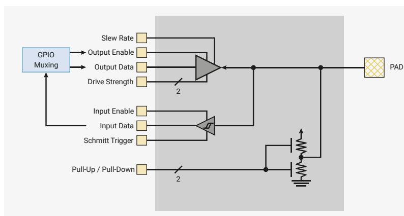
The diagram illustrates the internal structure of a single IO pad. On the left, a 'GPIO Muxing' block is connected to several control signals: Slew Rate, Output Enable, Output Data, Drive Strength (with a '2' indicating a 2-bit bus), Input Enable, Input Data, Schmitt Trigger, and Pull-Up / Pull-Down (also with a '2'). These signals are connected to a central logic block. This block contains an output driver (a PMOS and NMOS transistor pair) and an input buffer (a PMOS and NMOS transistor pair). The output driver's gate is controlled by Output Enable and Output Data. The input buffer's gate is controlled by Input Enable and Input Data. The Schmitt Trigger signal is connected to the input buffer. The Pull-Up / Pull-Down signal is connected to a pull-up/pull-down resistor network. The output of the output driver and the input of the input buffer are connected to the 'PAD' terminal on the right.
The pad's Output Enable, Output Data and Input Data ports are connected, via the IO mux, to the function controlling the pad. All other ports are controlled from the pad control register. The register also allows the pad's output driver to be disabled, by overriding the Output Enable signal from the function controlling the pad. See GPIO0 for an example of a pad control register.
Both the output signal level and acceptable input signal level at the pad are determined by the digital IO supply (IOVDD). IOVDD can be any nominal voltage between 1.8V and 3.3V, but to meet specification when powered at 1.8V, the pad input thresholds must be adjusted by writing a 1 to the pad
VOLTAGE_SELECT
registers. By default the pad input thresholds are valid for an IOVDD voltage between 2.5V and 3.3V. Using a voltage of 1.8V with the default input thresholds is a safe operating mode, though it will result in input thresholds that don't meet specification.
⚠ WARNING
Using IOVDD voltages greater than 1.8V, with the input thresholds set for 1.8V may result in damage to the chip.
Pad input threshold are adjusted on a per bank basis, with separate
VOLTAGE_SELECT
registers for the pads associated with the User IO bank (IO Bank 0) and the QSPI IO bank. However, both banks share the same digital IO supply (IOVDD), so both register should always be set to the same value.
Pad register details are available in Section 2.19.6.3, "Pad Control - User Bank" and Section 2.19.6.4, "Pad Control - QSPI Bank" .
2.19.4.1. Bus Keeper Mode
For each pad, only the pull-up or the pull-down resistor can be enabled at any given time. It is impossible to enable both simultaneously. Instead, if you set both the
GPIO0.PDE
and
GPIO0.PUE
bits simultaneously then you enable
bus keeper
mode, where the pad is:
- • pulled up when its input is high, and
- • pulled down when its input is low
When the output buffer is disabled, and the pad is not driven by any external source, this mode weakly retains the pad's current logical state. The pad does not float to mid-rail.
2.19.5. Software Examples
2.19.5.1. Select an IO function
An IO pin can perform many different functions and must be configured before use. For example, you may want it to be a
UART_TX
pin, or a
PWM
output. The SDK provides
gpio_set_function
for this purpose. Many SDK examples will call
gpio_set_function
at the beginning so that it can print to a UART.
The SDK starts by defining a structure to represent the registers of IO bank 0, the User IO bank. Each IO has a status register, followed by a control register. There are 30 IOs, so the structure containing a status and control register is instantiated as
io[30]
to repeat it 30 times.
SDK: https://github.com/raspberrypi/pico-sdk/blob/master/src/rp2040/hardware_structs/include/hardware_structs/io_bank0.h Lines 181 - 229
181 typedef struct {
182     io_bank0_status_ctrl_hw_t io[30];
183
184     // (Description copied from array index 0 register IO_BANK0_INTR0 applies similarly to
185     // other array indexes)
186     _REG_(IO_BANK0_INTR0_OFFSET) // IO_BANK0_INTR0
187     // Raw Interrupts
188     // 0x80000000 [31]    GPIO7_EDGE_HIGH (0)
189     // 0x40000000 [30]    GPIO7_EDGE_LOW (0)
190     // 0x20000000 [29]    GPIO7_LEVEL_HIGH (0)
191     // 0x10000000 [28]    GPIO7_LEVEL_LOW (0)
192     // 0x08000000 [27]    GPIO6_EDGE_HIGH (0)
193     // 0x04000000 [26]    GPIO6_EDGE_LOW (0)
194     // 0x02000000 [25]    GPIO6_LEVEL_HIGH (0)
195     // 0x01000000 [24]    GPIO6_LEVEL_LOW (0)
196     // 0x00800000 [23]    GPIO5_EDGE_HIGH (0)
197     // 0x00400000 [22]    GPIO5_EDGE_LOW (0)
198     // 0x00200000 [21]    GPIO5_LEVEL_HIGH (0)
199     // 0x00100000 [20]    GPIO5_LEVEL_LOW (0)
200     // 0x00080000 [19]    GPIO4_EDGE_HIGH (0)
201     // 0x00040000 [18]    GPIO4_EDGE_LOW (0)
202     // 0x00020000 [17]    GPIO4_LEVEL_HIGH (0)
203     // 0x00010000 [16]    GPIO4_LEVEL_LOW (0)
204     // 0x00008000 [15]    GPIO3_EDGE_HIGH (0)
205     // 0x00004000 [14]    GPIO3_EDGE_LOW (0)
206     // 0x00002000 [13]    GPIO3_LEVEL_HIGH (0)
207     // 0x00001000 [12]    GPIO3_LEVEL_LOW (0)
208     // 0x00000800 [11]    GPIO2_EDGE_HIGH (0)
209     // 0x00000400 [10]    GPIO2_EDGE_LOW (0)
210     // 0x00000200 [9]     GPIO2_LEVEL_HIGH (0)
211     // 0x00000100 [8]     GPIO2_LEVEL_LOW (0)
212     // 0x00000080 [7]     GPIO1_EDGE_HIGH (0)
213     // 0x00000040 [6]     GPIO1_EDGE_LOW (0)
214     // 0x00000020 [5]     GPIO1_LEVEL_HIGH (0)
215     // 0x00000010 [4]     GPIO1_LEVEL_LOW (0)
216     // 0x00000008 [3]     GPIO0_EDGE_HIGH (0)
217     // 0x00000004 [2]     GPIO0_EDGE_LOW (0)
217 // 0x00000002 [1]      GPIO0_LEVEL_HIGH (0)
218 // 0x00000001 [0]      GPIO0_LEVEL_LOW (0)
219 io_rw_32 intr[4];
220
221 union {
222     struct {
223         io_bank0_irq_ctrl_hw_t proc0_irq_ctrl;
224         io_bank0_irq_ctrl_hw_t proc1_irq_ctrl;
225         io_bank0_irq_ctrl_hw_t dormant_wake_irq_ctrl;
226     };
227     io_bank0_irq_ctrl_hw_t irq_ctrl[3];
228 };
229 } io_bank0_hw_t;
A similar structure is defined for the pad control registers for IO bank 1. By default, all pads come out of reset ready to use, with their input enabled and output disable set to 0. Regardless,
gpio_set_function
in the SDK sets these to make sure the pad is ready to use by the selected function. Finally, the desired function select is written to the IO control register (see
GPIO0_CTRL
for an example of an IO control register).
SDK: https://github.com/raspberrypi/pico-sdk/blob/master/src/rp2_common/hardware_gpio/gpio.c Lines 36 - 53
36 // Select function for this GPIO, and ensure input/output are enabled at the pad.
37 // This also clears the input/output/irq override bits.
38 void gpio_set_function(uint gpio, gpio_function_t fn) {
39     check_gpio_param(gpio);
40     invalid_params_if(HARDWARE_GPIO, ((uint32_t)fn << IO_BANK0_GPIO0_CTRL_FUNCSEL_LSB) &
~IO_BANK0_GPIO0_CTRL_FUNCSEL_BITS);
41     // Set input enable on, output disable off
42     hw_write_masked(&pads_bank0_hw->io[gpio],
43                     PADS_BANK0_GPIO0_IE_BITS,
44                     PADS_BANK0_GPIO0_IE_BITS | PADS_BANK0_GPIO0_OD_BITS
45 );
46     // Zero all fields apart from fsel; we want this IO to do what the peripheral tells it.
47     // This doesn't affect e.g. pullup/pulldown, as these are in pad controls.
48     io_bank0_hw->io[gpio].ctrl = fn << IO_BANK0_GPIO0_CTRL_FUNCSEL_LSB;
49 }
2.19.5.2. Enable a GPIO interrupt
The SDK provides a method of being interrupted when a GPIO pin changes state:
SDK: https://github.com/raspberrypi/pico-sdk/blob/master/src/rp2_common/hardware_gpio/gpio.c Lines 186 - 196
186 void gpio_set_irq_enabled(uint gpio, uint32_t events, bool enabled) {
187     // either this call disables the interrupt or callback should already be set.
188     // this protects against enabling the interrupt without callback set
189     assert(!enabled || irq_has_handler(IO_IRQ_BANK0));
190
191     // Separate mask/force/status per-core, so check which core called, and
192     // set the relevant IRQ controls.
193     io_bank0_irq_ctrl_hw_t *irq_ctrl_base = get_core_num() ?
194                                         &io_bank0_hw->proc1_irq_ctrl : &io_bank0_hw-
>proc0_irq_ctrl;
195     _gpio_set_irq_enabled(gpio, events, enabled, irq_ctrl_base);
196 }
gpio_set_irq_enabled
uses a lower level function
_gpio_set_irq_enabled
:
SDK: https://github.com/raspberrypi/pico-sdk/blob/master/src/rp2-common/hardware_gpio/gpio.c Lines 173 - 184
173 static void _gpio_set_irq_enabled(uint gpio, uint32_t events, bool enabled,
    io_bank0_irq_ctrl_hw_t *irq_ctrl_base) {
174     // Clear stale events which might cause immediate spurious handler entry
175     gpio_acknowledge_irq(gpio, events);
176
177     io_rw_32 *en_reg = &irq_ctrl_base->inte[gpio / 8];
178     events <=<= 4 * (gpio % 8);
179
180     if (enabled)
181         hw_set_bits(en_reg, events);
182     else
183         hw_clear_bits(en_reg, events);
184 }
The user provides a pointer to a callback function that is called when the GPIO event happens. An example application that uses this system is
hello_gpio_irq
:
Pico Examples: https://github.com/raspberrypi/pico-examples/blob/master/gpio/hello_gpio_irq/hello_gpio_irq.c
1 /**
2  * Copyright (c) 2020 Raspberry Pi (Trading) Ltd.
3  *
4  * SPDX-License-Identifier: BSD-3-Clause
5  */
6
7 #include <stdio.h>
8 #include "pico/stdlib.h"
9 #include "hardware/gpio.h"
10
11 #define GPIO_WATCH_PIN 2
12
13 static char event_str[128];
14
15 void gpio_event_string(char *buf, uint32_t events);
16
17 void gpio_callback(uint gpio, uint32_t events) {
18     // Put the GPIO event(s) that just happened into event_str
19     // so we can print it
20     gpio_event_string(event_str, events);
21     printf("GPIO %d %s\n", gpio, event_str);
22 }
23
24 int main() {
25     stdio_init_all();
26
27     printf("Hello GPIO IRQ\n");
28     gpio_init(GPIO_WATCH_PIN);
29     gpio_set_irq_enabled_with_callback(GPIO_WATCH_PIN, GPIO_IRQ_EDGE_RISE |
        GPIO_IRQ_EDGE_FALL, true, &gpio_callback);
30
31     // Wait forever
32     while (1);
33 }
34
35
36 static const char *gpio_irq_str[] = {
37     "LEVEL_LOW", // 0x1
38     "LEVEL_HIGH", // 0x2
39     "EDGE_FALL", // 0x4
40     "EDGE_RISE" // 0x8
41 };
42
43 void gpio_event_string(char *buf, uint32_t events) {
44     for (uint i = 0; i < 4; i++) {
45         uint mask = (1 << i);
46         if (events & mask) {
47             // Copy this event string into the user string
48             const char *event_str = gpio_irq_str[i];
49             while (*event_str != '\0') {
50                 *buf++ = *event_str++;
51             }
52             events &= ~mask;
53
54             // If more events add ", "
55             if (events) {
56                 *buf++ = ',';
57                 *buf++ = ' ';
58             }
59         }
60     }
61     *buf++ = '\0';
62 }
2.19.6. List of Registers
2.19.6.1. IO - User Bank
The User Bank IO registers start at a base address of 0x40014000 (defined as IO_BANK0_BASE in SDK).
Table 283. List of IO_BANK0 registers
| Offset | Name | Info |
|---|---|---|
| 0x000 | GPIO0_STATUS | GPIO status |
| 0x004 | GPIO0_CTRL | GPIO control including function select and overrides. |
| 0x008 | GPIO1_STATUS | GPIO status |
| 0x00c | GPIO1_CTRL | GPIO control including function select and overrides. |
| 0x010 | GPIO2_STATUS | GPIO status |
| 0x014 | GPIO2_CTRL | GPIO control including function select and overrides. |
| 0x018 | GPIO3_STATUS | GPIO status |
| 0x01c | GPIO3_CTRL | GPIO control including function select and overrides. |
| 0x020 | GPIO4_STATUS | GPIO status |
| 0x024 | GPIO4_CTRL | GPIO control including function select and overrides. |
| 0x028 | GPIO5_STATUS | GPIO status |
| 0x02c | GPIO5_CTRL | GPIO control including function select and overrides. |
| 0x030 | GPIO6_STATUS | GPIO status |
| 0x034 | GPIO6_CTRL | GPIO control including function select and overrides. |
| 0x038 | GPIO7_STATUS | GPIO status |
| 0x03c | GPIO7_CTRL | GPIO control including function select and overrides. |
| 0x040 | GPIO8_STATUS | GPIO status |
| Offset | Name | Info |
|---|---|---|
| 0x044 | GPIO8_CTRL | GPIO control including function select and overrides. |
| 0x048 | GPIO9_STATUS | GPIO status |
| 0x04c | GPIO9_CTRL | GPIO control including function select and overrides. |
| 0x050 | GPIO10_STATUS | GPIO status |
| 0x054 | GPIO10_CTRL | GPIO control including function select and overrides. |
| 0x058 | GPIO11_STATUS | GPIO status |
| 0x05c | GPIO11_CTRL | GPIO control including function select and overrides. |
| 0x060 | GPIO12_STATUS | GPIO status |
| 0x064 | GPIO12_CTRL | GPIO control including function select and overrides. |
| 0x068 | GPIO13_STATUS | GPIO status |
| 0x06c | GPIO13_CTRL | GPIO control including function select and overrides. |
| 0x070 | GPIO14_STATUS | GPIO status |
| 0x074 | GPIO14_CTRL | GPIO control including function select and overrides. |
| 0x078 | GPIO15_STATUS | GPIO status |
| 0x07c | GPIO15_CTRL | GPIO control including function select and overrides. |
| 0x080 | GPIO16_STATUS | GPIO status |
| 0x084 | GPIO16_CTRL | GPIO control including function select and overrides. |
| 0x088 | GPIO17_STATUS | GPIO status |
| 0x08c | GPIO17_CTRL | GPIO control including function select and overrides. |
| 0x090 | GPIO18_STATUS | GPIO status |
| 0x094 | GPIO18_CTRL | GPIO control including function select and overrides. |
| 0x098 | GPIO19_STATUS | GPIO status |
| 0x09c | GPIO19_CTRL | GPIO control including function select and overrides. |
| 0x0a0 | GPIO20_STATUS | GPIO status |
| 0x0a4 | GPIO20_CTRL | GPIO control including function select and overrides. |
| 0x0a8 | GPIO21_STATUS | GPIO status |
| 0x0ac | GPIO21_CTRL | GPIO control including function select and overrides. |
| 0x0b0 | GPIO22_STATUS | GPIO status |
| 0x0b4 | GPIO22_CTRL | GPIO control including function select and overrides. |
| 0x0b8 | GPIO23_STATUS | GPIO status |
| 0x0bc | GPIO23_CTRL | GPIO control including function select and overrides. |
| 0x0c0 | GPIO24_STATUS | GPIO status |
| 0x0c4 | GPIO24_CTRL | GPIO control including function select and overrides. |
| 0x0c8 | GPIO25_STATUS | GPIO status |
| 0x0cc | GPIO25_CTRL | GPIO control including function select and overrides. |
| 0x0d0 | GPIO26_STATUS | GPIO status |
| Offset | Name | Info |
|---|---|---|
| 0x0d4 | GPIO26_CTRL | GPIO control including function select and overrides. |
| 0x0d8 | GPIO27_STATUS | GPIO status |
| 0x0dc | GPIO27_CTRL | GPIO control including function select and overrides. |
| 0x0e0 | GPIO28_STATUS | GPIO status |
| 0x0e4 | GPIO28_CTRL | GPIO control including function select and overrides. |
| 0x0e8 | GPIO29_STATUS | GPIO status |
| 0x0ec | GPIO29_CTRL | GPIO control including function select and overrides. |
| 0x0f0 | INTR0 | Raw Interrupts |
| 0x0f4 | INTR1 | Raw Interrupts |
| 0x0f8 | INTR2 | Raw Interrupts |
| 0x0fc | INTR3 | Raw Interrupts |
| 0x100 | PROC0_INTE0 | Interrupt Enable for proc0 |
| 0x104 | PROC0_INTE1 | Interrupt Enable for proc0 |
| 0x108 | PROC0_INTE2 | Interrupt Enable for proc0 |
| 0x10c | PROC0_INTE3 | Interrupt Enable for proc0 |
| 0x110 | PROC0_INTF0 | Interrupt Force for proc0 |
| 0x114 | PROC0_INTF1 | Interrupt Force for proc0 |
| 0x118 | PROC0_INTF2 | Interrupt Force for proc0 |
| 0x11c | PROC0_INTF3 | Interrupt Force for proc0 |
| 0x120 | PROC0_INTS0 | Interrupt status after masking & forcing for proc0 |
| 0x124 | PROC0_INTS1 | Interrupt status after masking & forcing for proc0 |
| 0x128 | PROC0_INTS2 | Interrupt status after masking & forcing for proc0 |
| 0x12c | PROC0_INTS3 | Interrupt status after masking & forcing for proc0 |
| 0x130 | PROC1_INTE0 | Interrupt Enable for proc1 |
| 0x134 | PROC1_INTE1 | Interrupt Enable for proc1 |
| 0x138 | PROC1_INTE2 | Interrupt Enable for proc1 |
| 0x13c | PROC1_INTE3 | Interrupt Enable for proc1 |
| 0x140 | PROC1_INTF0 | Interrupt Force for proc1 |
| 0x144 | PROC1_INTF1 | Interrupt Force for proc1 |
| 0x148 | PROC1_INTF2 | Interrupt Force for proc1 |
| 0x14c | PROC1_INTF3 | Interrupt Force for proc1 |
| 0x150 | PROC1_INTS0 | Interrupt status after masking & forcing for proc1 |
| 0x154 | PROC1_INTS1 | Interrupt status after masking & forcing for proc1 |
| 0x158 | PROC1_INTS2 | Interrupt status after masking & forcing for proc1 |
| 0x15c | PROC1_INTS3 | Interrupt status after masking & forcing for proc1 |
| 0x160 | DORMANT_WAKE_INTE0 | Interrupt Enable for dormant_wake |
| Offset | Name | Info |
|---|---|---|
| 0x164 | DORMANT_WAKE_INTE1 | Interrupt Enable for dormant_wake |
| 0x168 | DORMANT_WAKE_INTE2 | Interrupt Enable for dormant_wake |
| 0x16c | DORMANT_WAKE_INTE3 | Interrupt Enable for dormant_wake |
| 0x170 | DORMANT_WAKE_INTF0 | Interrupt Force for dormant_wake |
| 0x174 | DORMANT_WAKE_INTF1 | Interrupt Force for dormant_wake |
| 0x178 | DORMANT_WAKE_INTF2 | Interrupt Force for dormant_wake |
| 0x17c | DORMANT_WAKE_INTF3 | Interrupt Force for dormant_wake |
| 0x180 | DORMANT_WAKE_INTS0 | Interrupt status after masking & forcing for dormant_wake |
| 0x184 | DORMANT_WAKE_INTS1 | Interrupt status after masking & forcing for dormant_wake |
| 0x188 | DORMANT_WAKE_INTS2 | Interrupt status after masking & forcing for dormant_wake |
| 0x18c | DORMANT_WAKE_INTS3 | Interrupt status after masking & forcing for dormant_wake |
IO_BANK0: GPIO0_STATUS, GPIO1_STATUS, ..., GPIO28_STATUS, GPIO29_STATUS Registers
Offsets: 0x000, 0x008, ..., 0x0e0, 0x0e8
Description
GPIO status
Table 284.
GPIO0_STATUS,
GPIO1_STATUS, ...,
GPIO28_STATUS,
GPIO29_STATUS
Registers
| Bits | Description | Type | Reset |
|---|---|---|---|
| 31:27 | Reserved. | - | - |
| 26 | IRQTOPROC : interrupt to processors, after override is applied | RO | 0x0 |
| 25 | Reserved. | - | - |
| 24 | IRQFROMPAD : interrupt from pad before override is applied | RO | 0x0 |
| 23:20 | Reserved. | - | - |
| 19 | INTOPERI : input signal to peripheral, after override is applied | RO | 0x0 |
| 18 | Reserved. | - | - |
| 17 | INFROMPAD : input signal from pad, before override is applied | RO | 0x0 |
| 16:14 | Reserved. | - | - |
| 13 | OETOPAD : output enable to pad after register override is applied | RO | 0x0 |
| 12 | OEFROMPERI : output enable from selected peripheral, before register override is applied | RO | 0x0 |
| 11:10 | Reserved. | - | - |
| 9 | OUTTOPAD : output signal to pad after register override is applied | RO | 0x0 |
| 8 | OUTFROMPERI : output signal from selected peripheral, before register override is applied | RO | 0x0 |
| 7:0 | Reserved. | - | - |
IO_BANK0: GPIO0_CTRL, GPIO1_CTRL, ..., GPIO28_CTRL, GPIO29_CTRL
Registers
Offsets: 0x004, 0x00c, ..., 0x0e4, 0x0ec
Description
GPIO control including function select and overrides.
Table 285.
GPIO0_CTRL,
GPIO1_CTRL, ...,
GPIO28_CTRL,
GPIO29_CTRL
Registers
| Bits | Description | Type | Reset |
|---|---|---|---|
| 31:30 | Reserved. | - | - |
| 29:28 | IRQOVER | RW | 0x0 |
| Enumerated values: | |||
| 0x0 → NORMAL: don't invert the interrupt | |||
| 0x1 → INVERT: invert the interrupt | |||
| 0x2 → LOW: drive interrupt low | |||
| 0x3 → HIGH: drive interrupt high | |||
| 27:18 | Reserved. | - | - |
| 17:16 | INOVER | RW | 0x0 |
| Enumerated values: | |||
| 0x0 → NORMAL: don't invert the peri input | |||
| 0x1 → INVERT: invert the peri input | |||
| 0x2 → LOW: drive peri input low | |||
| 0x3 → HIGH: drive peri input high | |||
| 15:14 | Reserved. | - | - |
| 13:12 | OEOVER | RW | 0x0 |
| Enumerated values: | |||
| 0x0 → NORMAL: drive output enable from peripheral signal selected by funcsel | |||
| 0x1 → INVERT: drive output enable from inverse of peripheral signal selected by funcsel | |||
| 0x2 → DISABLE: disable output | |||
| 0x3 → ENABLE: enable output | |||
| 11:10 | Reserved. | - | - |
| 9:8 | OUTOVER | RW | 0x0 |
| Enumerated values: | |||
| 0x0 → NORMAL: drive output from peripheral signal selected by funcsel | |||
| 0x1 → INVERT: drive output from inverse of peripheral signal selected by funcsel | |||
| 0x2 → LOW: drive output low | |||
| 0x3 → HIGH: drive output high | |||
| 7:5 | Reserved. | - | - |
| Bits | Description | Type | Reset |
|---|---|---|---|
| 4:0 | FUNCSEL : Function select. 31 == NULL. See GPIO function table for available functions. | RW | 0x1f |
IO_BANK0: INTR0 Register
Offset: 0x0f0
Description
Raw Interrupts
Table 286. INTR0 Register
| Bits | Description | Type | Reset |
|---|---|---|---|
| 31 | GPIO7_EDGE_HIGH | WC | 0x0 |
| 30 | GPIO7_EDGE_LOW | WC | 0x0 |
| 29 | GPIO7_LEVEL_HIGH | RO | 0x0 |
| 28 | GPIO7_LEVEL_LOW | RO | 0x0 |
| 27 | GPIO6_EDGE_HIGH | WC | 0x0 |
| 26 | GPIO6_EDGE_LOW | WC | 0x0 |
| 25 | GPIO6_LEVEL_HIGH | RO | 0x0 |
| 24 | GPIO6_LEVEL_LOW | RO | 0x0 |
| 23 | GPIO5_EDGE_HIGH | WC | 0x0 |
| 22 | GPIO5_EDGE_LOW | WC | 0x0 |
| 21 | GPIO5_LEVEL_HIGH | RO | 0x0 |
| 20 | GPIO5_LEVEL_LOW | RO | 0x0 |
| 19 | GPIO4_EDGE_HIGH | WC | 0x0 |
| 18 | GPIO4_EDGE_LOW | WC | 0x0 |
| 17 | GPIO4_LEVEL_HIGH | RO | 0x0 |
| 16 | GPIO4_LEVEL_LOW | RO | 0x0 |
| 15 | GPIO3_EDGE_HIGH | WC | 0x0 |
| 14 | GPIO3_EDGE_LOW | WC | 0x0 |
| 13 | GPIO3_LEVEL_HIGH | RO | 0x0 |
| 12 | GPIO3_LEVEL_LOW | RO | 0x0 |
| 11 | GPIO2_EDGE_HIGH | WC | 0x0 |
| 10 | GPIO2_EDGE_LOW | WC | 0x0 |
| 9 | GPIO2_LEVEL_HIGH | RO | 0x0 |
| 8 | GPIO2_LEVEL_LOW | RO | 0x0 |
| 7 | GPIO1_EDGE_HIGH | WC | 0x0 |
| 6 | GPIO1_EDGE_LOW | WC | 0x0 |
| 5 | GPIO1_LEVEL_HIGH | RO | 0x0 |
| 4 | GPIO1_LEVEL_LOW | RO | 0x0 |
| 3 | GPIO0_EDGE_HIGH | WC | 0x0 |
| Bits | Description | Type | Reset |
|---|---|---|---|
| 2 | GPIO0_EDGE_LOW | WC | 0x0 |
| 1 | GPIO0_LEVEL_HIGH | RO | 0x0 |
| 0 | GPIO0_LEVEL_LOW | RO | 0x0 |
IO_BANK0: INTR1 Register
Offset: 0x0f4
Description
Raw Interrupts
Table 287. INTR1 Register
| Bits | Description | Type | Reset |
|---|---|---|---|
| 31 | GPIO15_EDGE_HIGH | WC | 0x0 |
| 30 | GPIO15_EDGE_LOW | WC | 0x0 |
| 29 | GPIO15_LEVEL_HIGH | RO | 0x0 |
| 28 | GPIO15_LEVEL_LOW | RO | 0x0 |
| 27 | GPIO14_EDGE_HIGH | WC | 0x0 |
| 26 | GPIO14_EDGE_LOW | WC | 0x0 |
| 25 | GPIO14_LEVEL_HIGH | RO | 0x0 |
| 24 | GPIO14_LEVEL_LOW | RO | 0x0 |
| 23 | GPIO13_EDGE_HIGH | WC | 0x0 |
| 22 | GPIO13_EDGE_LOW | WC | 0x0 |
| 21 | GPIO13_LEVEL_HIGH | RO | 0x0 |
| 20 | GPIO13_LEVEL_LOW | RO | 0x0 |
| 19 | GPIO12_EDGE_HIGH | WC | 0x0 |
| 18 | GPIO12_EDGE_LOW | WC | 0x0 |
| 17 | GPIO12_LEVEL_HIGH | RO | 0x0 |
| 16 | GPIO12_LEVEL_LOW | RO | 0x0 |
| 15 | GPIO11_EDGE_HIGH | WC | 0x0 |
| 14 | GPIO11_EDGE_LOW | WC | 0x0 |
| 13 | GPIO11_LEVEL_HIGH | RO | 0x0 |
| 12 | GPIO11_LEVEL_LOW | RO | 0x0 |
| 11 | GPIO10_EDGE_HIGH | WC | 0x0 |
| 10 | GPIO10_EDGE_LOW | WC | 0x0 |
| 9 | GPIO10_LEVEL_HIGH | RO | 0x0 |
| 8 | GPIO10_LEVEL_LOW | RO | 0x0 |
| 7 | GPIO9_EDGE_HIGH | WC | 0x0 |
| 6 | GPIO9_EDGE_LOW | WC | 0x0 |
| 5 | GPIO9_LEVEL_HIGH | RO | 0x0 |
| Bits | Description | Type | Reset |
|---|---|---|---|
| 4 | GPIO9_LEVEL_LOW | RO | 0x0 |
| 3 | GPIO8_EDGE_HIGH | WC | 0x0 |
| 2 | GPIO8_EDGE_LOW | WC | 0x0 |
| 1 | GPIO8_LEVEL_HIGH | RO | 0x0 |
| 0 | GPIO8_LEVEL_LOW | RO | 0x0 |
IO_BANK0: INTR2 Register
Offset: 0x0f8
Description
Raw Interrupts
Table 288. INTR2 Register
| Bits | Description | Type | Reset |
|---|---|---|---|
| 31 | GPIO23_EDGE_HIGH | WC | 0x0 |
| 30 | GPIO23_EDGE_LOW | WC | 0x0 |
| 29 | GPIO23_LEVEL_HIGH | RO | 0x0 |
| 28 | GPIO23_LEVEL_LOW | RO | 0x0 |
| 27 | GPIO22_EDGE_HIGH | WC | 0x0 |
| 26 | GPIO22_EDGE_LOW | WC | 0x0 |
| 25 | GPIO22_LEVEL_HIGH | RO | 0x0 |
| 24 | GPIO22_LEVEL_LOW | RO | 0x0 |
| 23 | GPIO21_EDGE_HIGH | WC | 0x0 |
| 22 | GPIO21_EDGE_LOW | WC | 0x0 |
| 21 | GPIO21_LEVEL_HIGH | RO | 0x0 |
| 20 | GPIO21_LEVEL_LOW | RO | 0x0 |
| 19 | GPIO20_EDGE_HIGH | WC | 0x0 |
| 18 | GPIO20_EDGE_LOW | WC | 0x0 |
| 17 | GPIO20_LEVEL_HIGH | RO | 0x0 |
| 16 | GPIO20_LEVEL_LOW | RO | 0x0 |
| 15 | GPIO19_EDGE_HIGH | WC | 0x0 |
| 14 | GPIO19_EDGE_LOW | WC | 0x0 |
| 13 | GPIO19_LEVEL_HIGH | RO | 0x0 |
| 12 | GPIO19_LEVEL_LOW | RO | 0x0 |
| 11 | GPIO18_EDGE_HIGH | WC | 0x0 |
| 10 | GPIO18_EDGE_LOW | WC | 0x0 |
| 9 | GPIO18_LEVEL_HIGH | RO | 0x0 |
| 8 | GPIO18_LEVEL_LOW | RO | 0x0 |
| 7 | GPIO17_EDGE_HIGH | WC | 0x0 |
| Bits | Description | Type | Reset |
|---|---|---|---|
| 6 | GPIO17_EDGE_LOW | WC | 0x0 |
| 5 | GPIO17_LEVEL_HIGH | RO | 0x0 |
| 4 | GPIO17_LEVEL_LOW | RO | 0x0 |
| 3 | GPIO16_EDGE_HIGH | WC | 0x0 |
| 2 | GPIO16_EDGE_LOW | WC | 0x0 |
| 1 | GPIO16_LEVEL_HIGH | RO | 0x0 |
| 0 | GPIO16_LEVEL_LOW | RO | 0x0 |
IO_BANK0: INTR3 Register
Offset: 0x0fc
Description
Raw Interrupts
Table 289. INTR3 Register
| Bits | Description | Type | Reset |
|---|---|---|---|
| 31:24 | Reserved. | - | - |
| 23 | GPIO29_EDGE_HIGH | WC | 0x0 |
| 22 | GPIO29_EDGE_LOW | WC | 0x0 |
| 21 | GPIO29_LEVEL_HIGH | RO | 0x0 |
| 20 | GPIO29_LEVEL_LOW | RO | 0x0 |
| 19 | GPIO28_EDGE_HIGH | WC | 0x0 |
| 18 | GPIO28_EDGE_LOW | WC | 0x0 |
| 17 | GPIO28_LEVEL_HIGH | RO | 0x0 |
| 16 | GPIO28_LEVEL_LOW | RO | 0x0 |
| 15 | GPIO27_EDGE_HIGH | WC | 0x0 |
| 14 | GPIO27_EDGE_LOW | WC | 0x0 |
| 13 | GPIO27_LEVEL_HIGH | RO | 0x0 |
| 12 | GPIO27_LEVEL_LOW | RO | 0x0 |
| 11 | GPIO26_EDGE_HIGH | WC | 0x0 |
| 10 | GPIO26_EDGE_LOW | WC | 0x0 |
| 9 | GPIO26_LEVEL_HIGH | RO | 0x0 |
| 8 | GPIO26_LEVEL_LOW | RO | 0x0 |
| 7 | GPIO25_EDGE_HIGH | WC | 0x0 |
| 6 | GPIO25_EDGE_LOW | WC | 0x0 |
| 5 | GPIO25_LEVEL_HIGH | RO | 0x0 |
| 4 | GPIO25_LEVEL_LOW | RO | 0x0 |
| 3 | GPIO24_EDGE_HIGH | WC | 0x0 |
| 2 | GPIO24_EDGE_LOW | WC | 0x0 |
| Bits | Description | Type | Reset |
|---|---|---|---|
| 1 | GPIO24_LEVEL_HIGH | RO | 0x0 |
| 0 | GPIO24_LEVEL_LOW | RO | 0x0 |
IO_BANK0: PROC0_INTE0 Register
Offset: 0x100
Description
Interrupt Enable for proc0
Table 290.
PROC0_INTE0 Register
| Bits | Description | Type | Reset |
|---|---|---|---|
| 31 | GPIO7_EDGE_HIGH | RW | 0x0 |
| 30 | GPIO7_EDGE_LOW | RW | 0x0 |
| 29 | GPIO7_LEVEL_HIGH | RW | 0x0 |
| 28 | GPIO7_LEVEL_LOW | RW | 0x0 |
| 27 | GPIO6_EDGE_HIGH | RW | 0x0 |
| 26 | GPIO6_EDGE_LOW | RW | 0x0 |
| 25 | GPIO6_LEVEL_HIGH | RW | 0x0 |
| 24 | GPIO6_LEVEL_LOW | RW | 0x0 |
| 23 | GPIO5_EDGE_HIGH | RW | 0x0 |
| 22 | GPIO5_EDGE_LOW | RW | 0x0 |
| 21 | GPIO5_LEVEL_HIGH | RW | 0x0 |
| 20 | GPIO5_LEVEL_LOW | RW | 0x0 |
| 19 | GPIO4_EDGE_HIGH | RW | 0x0 |
| 18 | GPIO4_EDGE_LOW | RW | 0x0 |
| 17 | GPIO4_LEVEL_HIGH | RW | 0x0 |
| 16 | GPIO4_LEVEL_LOW | RW | 0x0 |
| 15 | GPIO3_EDGE_HIGH | RW | 0x0 |
| 14 | GPIO3_EDGE_LOW | RW | 0x0 |
| 13 | GPIO3_LEVEL_HIGH | RW | 0x0 |
| 12 | GPIO3_LEVEL_LOW | RW | 0x0 |
| 11 | GPIO2_EDGE_HIGH | RW | 0x0 |
| 10 | GPIO2_EDGE_LOW | RW | 0x0 |
| 9 | GPIO2_LEVEL_HIGH | RW | 0x0 |
| 8 | GPIO2_LEVEL_LOW | RW | 0x0 |
| 7 | GPIO1_EDGE_HIGH | RW | 0x0 |
| 6 | GPIO1_EDGE_LOW | RW | 0x0 |
| 5 | GPIO1_LEVEL_HIGH | RW | 0x0 |
| 4 | GPIO1_LEVEL_LOW | RW | 0x0 |
| Bits | Description | Type | Reset |
|---|---|---|---|
| 3 | GPIO0_EDGE_HIGH | RW | 0x0 |
| 2 | GPIO0_EDGE_LOW | RW | 0x0 |
| 1 | GPIO0_LEVEL_HIGH | RW | 0x0 |
| 0 | GPIO0_LEVEL_LOW | RW | 0x0 |
IO_BANK0: PROC0_INTE1 Register
Offset: 0x104
Description
Interrupt Enable for proc0
Table 291.
PROC0_INTE1 Register
| Bits | Description | Type | Reset |
|---|---|---|---|
| 31 | GPIO15_EDGE_HIGH | RW | 0x0 |
| 30 | GPIO15_EDGE_LOW | RW | 0x0 |
| 29 | GPIO15_LEVEL_HIGH | RW | 0x0 |
| 28 | GPIO15_LEVEL_LOW | RW | 0x0 |
| 27 | GPIO14_EDGE_HIGH | RW | 0x0 |
| 26 | GPIO14_EDGE_LOW | RW | 0x0 |
| 25 | GPIO14_LEVEL_HIGH | RW | 0x0 |
| 24 | GPIO14_LEVEL_LOW | RW | 0x0 |
| 23 | GPIO13_EDGE_HIGH | RW | 0x0 |
| 22 | GPIO13_EDGE_LOW | RW | 0x0 |
| 21 | GPIO13_LEVEL_HIGH | RW | 0x0 |
| 20 | GPIO13_LEVEL_LOW | RW | 0x0 |
| 19 | GPIO12_EDGE_HIGH | RW | 0x0 |
| 18 | GPIO12_EDGE_LOW | RW | 0x0 |
| 17 | GPIO12_LEVEL_HIGH | RW | 0x0 |
| 16 | GPIO12_LEVEL_LOW | RW | 0x0 |
| 15 | GPIO11_EDGE_HIGH | RW | 0x0 |
| 14 | GPIO11_EDGE_LOW | RW | 0x0 |
| 13 | GPIO11_LEVEL_HIGH | RW | 0x0 |
| 12 | GPIO11_LEVEL_LOW | RW | 0x0 |
| 11 | GPIO10_EDGE_HIGH | RW | 0x0 |
| 10 | GPIO10_EDGE_LOW | RW | 0x0 |
| 9 | GPIO10_LEVEL_HIGH | RW | 0x0 |
| 8 | GPIO10_LEVEL_LOW | RW | 0x0 |
| 7 | GPIO9_EDGE_HIGH | RW | 0x0 |
| 6 | GPIO9_EDGE_LOW | RW | 0x0 |
| Bits | Description | Type | Reset |
|---|---|---|---|
| 5 | GPIO9_LEVEL_HIGH | RW | 0x0 |
| 4 | GPIO9_LEVEL_LOW | RW | 0x0 |
| 3 | GPIO8_EDGE_HIGH | RW | 0x0 |
| 2 | GPIO8_EDGE_LOW | RW | 0x0 |
| 1 | GPIO8_LEVEL_HIGH | RW | 0x0 |
| 0 | GPIO8_LEVEL_LOW | RW | 0x0 |
IO_BANK0: PROC0_INTE2 Register
Offset: 0x108
Description
Interrupt Enable for proc0
Table 292.
PROC0_INTE2 Register
| Bits | Description | Type | Reset |
|---|---|---|---|
| 31 | GPIO23_EDGE_HIGH | RW | 0x0 |
| 30 | GPIO23_EDGE_LOW | RW | 0x0 |
| 29 | GPIO23_LEVEL_HIGH | RW | 0x0 |
| 28 | GPIO23_LEVEL_LOW | RW | 0x0 |
| 27 | GPIO22_EDGE_HIGH | RW | 0x0 |
| 26 | GPIO22_EDGE_LOW | RW | 0x0 |
| 25 | GPIO22_LEVEL_HIGH | RW | 0x0 |
| 24 | GPIO22_LEVEL_LOW | RW | 0x0 |
| 23 | GPIO21_EDGE_HIGH | RW | 0x0 |
| 22 | GPIO21_EDGE_LOW | RW | 0x0 |
| 21 | GPIO21_LEVEL_HIGH | RW | 0x0 |
| 20 | GPIO21_LEVEL_LOW | RW | 0x0 |
| 19 | GPIO20_EDGE_HIGH | RW | 0x0 |
| 18 | GPIO20_EDGE_LOW | RW | 0x0 |
| 17 | GPIO20_LEVEL_HIGH | RW | 0x0 |
| 16 | GPIO20_LEVEL_LOW | RW | 0x0 |
| 15 | GPIO19_EDGE_HIGH | RW | 0x0 |
| 14 | GPIO19_EDGE_LOW | RW | 0x0 |
| 13 | GPIO19_LEVEL_HIGH | RW | 0x0 |
| 12 | GPIO19_LEVEL_LOW | RW | 0x0 |
| 11 | GPIO18_EDGE_HIGH | RW | 0x0 |
| 10 | GPIO18_EDGE_LOW | RW | 0x0 |
| 9 | GPIO18_LEVEL_HIGH | RW | 0x0 |
| 8 | GPIO18_LEVEL_LOW | RW | 0x0 |
| Bits | Description | Type | Reset |
|---|---|---|---|
| 7 | GPIO17_EDGE_HIGH | RW | 0x0 |
| 6 | GPIO17_EDGE_LOW | RW | 0x0 |
| 5 | GPIO17_LEVEL_HIGH | RW | 0x0 |
| 4 | GPIO17_LEVEL_LOW | RW | 0x0 |
| 3 | GPIO16_EDGE_HIGH | RW | 0x0 |
| 2 | GPIO16_EDGE_LOW | RW | 0x0 |
| 1 | GPIO16_LEVEL_HIGH | RW | 0x0 |
| 0 | GPIO16_LEVEL_LOW | RW | 0x0 |
IO_BANK0: PROC0_INTE3 Register
Offset: 0x10c
Description
Interrupt Enable for proc0
Table 293.
PROC0_INTE3 Register
| Bits | Description | Type | Reset |
|---|---|---|---|
| 31:24 | Reserved. | - | - |
| 23 | GPIO29_EDGE_HIGH | RW | 0x0 |
| 22 | GPIO29_EDGE_LOW | RW | 0x0 |
| 21 | GPIO29_LEVEL_HIGH | RW | 0x0 |
| 20 | GPIO29_LEVEL_LOW | RW | 0x0 |
| 19 | GPIO28_EDGE_HIGH | RW | 0x0 |
| 18 | GPIO28_EDGE_LOW | RW | 0x0 |
| 17 | GPIO28_LEVEL_HIGH | RW | 0x0 |
| 16 | GPIO28_LEVEL_LOW | RW | 0x0 |
| 15 | GPIO27_EDGE_HIGH | RW | 0x0 |
| 14 | GPIO27_EDGE_LOW | RW | 0x0 |
| 13 | GPIO27_LEVEL_HIGH | RW | 0x0 |
| 12 | GPIO27_LEVEL_LOW | RW | 0x0 |
| 11 | GPIO26_EDGE_HIGH | RW | 0x0 |
| 10 | GPIO26_EDGE_LOW | RW | 0x0 |
| 9 | GPIO26_LEVEL_HIGH | RW | 0x0 |
| 8 | GPIO26_LEVEL_LOW | RW | 0x0 |
| 7 | GPIO25_EDGE_HIGH | RW | 0x0 |
| 6 | GPIO25_EDGE_LOW | RW | 0x0 |
| 5 | GPIO25_LEVEL_HIGH | RW | 0x0 |
| 4 | GPIO25_LEVEL_LOW | RW | 0x0 |
| 3 | GPIO24_EDGE_HIGH | RW | 0x0 |
| Bits | Description | Type | Reset |
|---|---|---|---|
| 2 | GPIO24_EDGE_LOW | RW | 0x0 |
| 1 | GPIO24_LEVEL_HIGH | RW | 0x0 |
| 0 | GPIO24_LEVEL_LOW | RW | 0x0 |
IO_BANK0: PROC0_INTF0 Register
Offset: 0x110
Description
Interrupt Force for proc0
Table 294.
PROC0_INTF0 Register
| Bits | Description | Type | Reset |
|---|---|---|---|
| 31 | GPIO7_EDGE_HIGH | RW | 0x0 |
| 30 | GPIO7_EDGE_LOW | RW | 0x0 |
| 29 | GPIO7_LEVEL_HIGH | RW | 0x0 |
| 28 | GPIO7_LEVEL_LOW | RW | 0x0 |
| 27 | GPIO6_EDGE_HIGH | RW | 0x0 |
| 26 | GPIO6_EDGE_LOW | RW | 0x0 |
| 25 | GPIO6_LEVEL_HIGH | RW | 0x0 |
| 24 | GPIO6_LEVEL_LOW | RW | 0x0 |
| 23 | GPIO5_EDGE_HIGH | RW | 0x0 |
| 22 | GPIO5_EDGE_LOW | RW | 0x0 |
| 21 | GPIO5_LEVEL_HIGH | RW | 0x0 |
| 20 | GPIO5_LEVEL_LOW | RW | 0x0 |
| 19 | GPIO4_EDGE_HIGH | RW | 0x0 |
| 18 | GPIO4_EDGE_LOW | RW | 0x0 |
| 17 | GPIO4_LEVEL_HIGH | RW | 0x0 |
| 16 | GPIO4_LEVEL_LOW | RW | 0x0 |
| 15 | GPIO3_EDGE_HIGH | RW | 0x0 |
| 14 | GPIO3_EDGE_LOW | RW | 0x0 |
| 13 | GPIO3_LEVEL_HIGH | RW | 0x0 |
| 12 | GPIO3_LEVEL_LOW | RW | 0x0 |
| 11 | GPIO2_EDGE_HIGH | RW | 0x0 |
| 10 | GPIO2_EDGE_LOW | RW | 0x0 |
| 9 | GPIO2_LEVEL_HIGH | RW | 0x0 |
| 8 | GPIO2_LEVEL_LOW | RW | 0x0 |
| 7 | GPIO1_EDGE_HIGH | RW | 0x0 |
| 6 | GPIO1_EDGE_LOW | RW | 0x0 |
| 5 | GPIO1_LEVEL_HIGH | RW | 0x0 |
| Bits | Description | Type | Reset |
|---|---|---|---|
| 4 | GPIO1_LEVEL_LOW | RW | 0x0 |
| 3 | GPIO0_EDGE_HIGH | RW | 0x0 |
| 2 | GPIO0_EDGE_LOW | RW | 0x0 |
| 1 | GPIO0_LEVEL_HIGH | RW | 0x0 |
| 0 | GPIO0_LEVEL_LOW | RW | 0x0 |
IO_BANK0: PROC0_INTF1 Register
Offset: 0x114
Description
Interrupt Force for proc0
Table 295.
PROC0_INTF1 Register
| Bits | Description | Type | Reset |
|---|---|---|---|
| 31 | GPIO15_EDGE_HIGH | RW | 0x0 |
| 30 | GPIO15_EDGE_LOW | RW | 0x0 |
| 29 | GPIO15_LEVEL_HIGH | RW | 0x0 |
| 28 | GPIO15_LEVEL_LOW | RW | 0x0 |
| 27 | GPIO14_EDGE_HIGH | RW | 0x0 |
| 26 | GPIO14_EDGE_LOW | RW | 0x0 |
| 25 | GPIO14_LEVEL_HIGH | RW | 0x0 |
| 24 | GPIO14_LEVEL_LOW | RW | 0x0 |
| 23 | GPIO13_EDGE_HIGH | RW | 0x0 |
| 22 | GPIO13_EDGE_LOW | RW | 0x0 |
| 21 | GPIO13_LEVEL_HIGH | RW | 0x0 |
| 20 | GPIO13_LEVEL_LOW | RW | 0x0 |
| 19 | GPIO12_EDGE_HIGH | RW | 0x0 |
| 18 | GPIO12_EDGE_LOW | RW | 0x0 |
| 17 | GPIO12_LEVEL_HIGH | RW | 0x0 |
| 16 | GPIO12_LEVEL_LOW | RW | 0x0 |
| 15 | GPIO11_EDGE_HIGH | RW | 0x0 |
| 14 | GPIO11_EDGE_LOW | RW | 0x0 |
| 13 | GPIO11_LEVEL_HIGH | RW | 0x0 |
| 12 | GPIO11_LEVEL_LOW | RW | 0x0 |
| 11 | GPIO10_EDGE_HIGH | RW | 0x0 |
| 10 | GPIO10_EDGE_LOW | RW | 0x0 |
| 9 | GPIO10_LEVEL_HIGH | RW | 0x0 |
| 8 | GPIO10_LEVEL_LOW | RW | 0x0 |
| 7 | GPIO9_EDGE_HIGH | RW | 0x0 |
| Bits | Description | Type | Reset |
|---|---|---|---|
| 6 | GPIO9_EDGE_LOW | RW | 0x0 |
| 5 | GPIO9_LEVEL_HIGH | RW | 0x0 |
| 4 | GPIO9_LEVEL_LOW | RW | 0x0 |
| 3 | GPIO8_EDGE_HIGH | RW | 0x0 |
| 2 | GPIO8_EDGE_LOW | RW | 0x0 |
| 1 | GPIO8_LEVEL_HIGH | RW | 0x0 |
| 0 | GPIO8_LEVEL_LOW | RW | 0x0 |
IO_BANK0: PROC0_INTF2 Register
Offset: 0x118
Description
Interrupt Force for proc0
Table 296.
PROC0_INTF2 Register
| Bits | Description | Type | Reset |
|---|---|---|---|
| 31 | GPIO23_EDGE_HIGH | RW | 0x0 |
| 30 | GPIO23_EDGE_LOW | RW | 0x0 |
| 29 | GPIO23_LEVEL_HIGH | RW | 0x0 |
| 28 | GPIO23_LEVEL_LOW | RW | 0x0 |
| 27 | GPIO22_EDGE_HIGH | RW | 0x0 |
| 26 | GPIO22_EDGE_LOW | RW | 0x0 |
| 25 | GPIO22_LEVEL_HIGH | RW | 0x0 |
| 24 | GPIO22_LEVEL_LOW | RW | 0x0 |
| 23 | GPIO21_EDGE_HIGH | RW | 0x0 |
| 22 | GPIO21_EDGE_LOW | RW | 0x0 |
| 21 | GPIO21_LEVEL_HIGH | RW | 0x0 |
| 20 | GPIO21_LEVEL_LOW | RW | 0x0 |
| 19 | GPIO20_EDGE_HIGH | RW | 0x0 |
| 18 | GPIO20_EDGE_LOW | RW | 0x0 |
| 17 | GPIO20_LEVEL_HIGH | RW | 0x0 |
| 16 | GPIO20_LEVEL_LOW | RW | 0x0 |
| 15 | GPIO19_EDGE_HIGH | RW | 0x0 |
| 14 | GPIO19_EDGE_LOW | RW | 0x0 |
| 13 | GPIO19_LEVEL_HIGH | RW | 0x0 |
| 12 | GPIO19_LEVEL_LOW | RW | 0x0 |
| 11 | GPIO18_EDGE_HIGH | RW | 0x0 |
| 10 | GPIO18_EDGE_LOW | RW | 0x0 |
| 9 | GPIO18_LEVEL_HIGH | RW | 0x0 |
| Bits | Description | Type | Reset |
|---|---|---|---|
| 8 | GPIO18_LEVEL_LOW | RW | 0x0 |
| 7 | GPIO17_EDGE_HIGH | RW | 0x0 |
| 6 | GPIO17_EDGE_LOW | RW | 0x0 |
| 5 | GPIO17_LEVEL_HIGH | RW | 0x0 |
| 4 | GPIO17_LEVEL_LOW | RW | 0x0 |
| 3 | GPIO16_EDGE_HIGH | RW | 0x0 |
| 2 | GPIO16_EDGE_LOW | RW | 0x0 |
| 1 | GPIO16_LEVEL_HIGH | RW | 0x0 |
| 0 | GPIO16_LEVEL_LOW | RW | 0x0 |
IO_BANK0: PROC0_INTF3 Register
Offset: 0x11c
Description
Interrupt Force for proc0
Table 297.
PROC0_INTF3 Register
| Bits | Description | Type | Reset |
|---|---|---|---|
| 31:24 | Reserved. | - | - |
| 23 | GPIO29_EDGE_HIGH | RW | 0x0 |
| 22 | GPIO29_EDGE_LOW | RW | 0x0 |
| 21 | GPIO29_LEVEL_HIGH | RW | 0x0 |
| 20 | GPIO29_LEVEL_LOW | RW | 0x0 |
| 19 | GPIO28_EDGE_HIGH | RW | 0x0 |
| 18 | GPIO28_EDGE_LOW | RW | 0x0 |
| 17 | GPIO28_LEVEL_HIGH | RW | 0x0 |
| 16 | GPIO28_LEVEL_LOW | RW | 0x0 |
| 15 | GPIO27_EDGE_HIGH | RW | 0x0 |
| 14 | GPIO27_EDGE_LOW | RW | 0x0 |
| 13 | GPIO27_LEVEL_HIGH | RW | 0x0 |
| 12 | GPIO27_LEVEL_LOW | RW | 0x0 |
| 11 | GPIO26_EDGE_HIGH | RW | 0x0 |
| 10 | GPIO26_EDGE_LOW | RW | 0x0 |
| 9 | GPIO26_LEVEL_HIGH | RW | 0x0 |
| 8 | GPIO26_LEVEL_LOW | RW | 0x0 |
| 7 | GPIO25_EDGE_HIGH | RW | 0x0 |
| 6 | GPIO25_EDGE_LOW | RW | 0x0 |
| 5 | GPIO25_LEVEL_HIGH | RW | 0x0 |
| 4 | GPIO25_LEVEL_LOW | RW | 0x0 |
| Bits | Description | Type | Reset |
|---|---|---|---|
| 3 | GPIO24_EDGE_HIGH | RW | 0x0 |
| 2 | GPIO24_EDGE_LOW | RW | 0x0 |
| 1 | GPIO24_LEVEL_HIGH | RW | 0x0 |
| 0 | GPIO24_LEVEL_LOW | RW | 0x0 |
IO_BANK0: PROC0_INTS0 Register
Offset: 0x120
Description
Interrupt status after masking & forcing for proc0
Table 298.
PROC0_INTS0
Register
| Bits | Description | Type | Reset |
|---|---|---|---|
| 31 | GPIO7_EDGE_HIGH | RO | 0x0 |
| 30 | GPIO7_EDGE_LOW | RO | 0x0 |
| 29 | GPIO7_LEVEL_HIGH | RO | 0x0 |
| 28 | GPIO7_LEVEL_LOW | RO | 0x0 |
| 27 | GPIO6_EDGE_HIGH | RO | 0x0 |
| 26 | GPIO6_EDGE_LOW | RO | 0x0 |
| 25 | GPIO6_LEVEL_HIGH | RO | 0x0 |
| 24 | GPIO6_LEVEL_LOW | RO | 0x0 |
| 23 | GPIO5_EDGE_HIGH | RO | 0x0 |
| 22 | GPIO5_EDGE_LOW | RO | 0x0 |
| 21 | GPIO5_LEVEL_HIGH | RO | 0x0 |
| 20 | GPIO5_LEVEL_LOW | RO | 0x0 |
| 19 | GPIO4_EDGE_HIGH | RO | 0x0 |
| 18 | GPIO4_EDGE_LOW | RO | 0x0 |
| 17 | GPIO4_LEVEL_HIGH | RO | 0x0 |
| 16 | GPIO4_LEVEL_LOW | RO | 0x0 |
| 15 | GPIO3_EDGE_HIGH | RO | 0x0 |
| 14 | GPIO3_EDGE_LOW | RO | 0x0 |
| 13 | GPIO3_LEVEL_HIGH | RO | 0x0 |
| 12 | GPIO3_LEVEL_LOW | RO | 0x0 |
| 11 | GPIO2_EDGE_HIGH | RO | 0x0 |
| 10 | GPIO2_EDGE_LOW | RO | 0x0 |
| 9 | GPIO2_LEVEL_HIGH | RO | 0x0 |
| 8 | GPIO2_LEVEL_LOW | RO | 0x0 |
| 7 | GPIO1_EDGE_HIGH | RO | 0x0 |
| 6 | GPIO1_EDGE_LOW | RO | 0x0 |
| Bits | Description | Type | Reset |
|---|---|---|---|
| 5 | GPIO1_LEVEL_HIGH | RO | 0x0 |
| 4 | GPIO1_LEVEL_LOW | RO | 0x0 |
| 3 | GPIO0_EDGE_HIGH | RO | 0x0 |
| 2 | GPIO0_EDGE_LOW | RO | 0x0 |
| 1 | GPIO0_LEVEL_HIGH | RO | 0x0 |
| 0 | GPIO0_LEVEL_LOW | RO | 0x0 |
IO_BANK0: PROC0_INTS1 Register
Offset: 0x124
Description
Interrupt status after masking & forcing for proc0
Table 299.
PROC0_INTS1
Register
| Bits | Description | Type | Reset |
|---|---|---|---|
| 31 | GPIO15_EDGE_HIGH | RO | 0x0 |
| 30 | GPIO15_EDGE_LOW | RO | 0x0 |
| 29 | GPIO15_LEVEL_HIGH | RO | 0x0 |
| 28 | GPIO15_LEVEL_LOW | RO | 0x0 |
| 27 | GPIO14_EDGE_HIGH | RO | 0x0 |
| 26 | GPIO14_EDGE_LOW | RO | 0x0 |
| 25 | GPIO14_LEVEL_HIGH | RO | 0x0 |
| 24 | GPIO14_LEVEL_LOW | RO | 0x0 |
| 23 | GPIO13_EDGE_HIGH | RO | 0x0 |
| 22 | GPIO13_EDGE_LOW | RO | 0x0 |
| 21 | GPIO13_LEVEL_HIGH | RO | 0x0 |
| 20 | GPIO13_LEVEL_LOW | RO | 0x0 |
| 19 | GPIO12_EDGE_HIGH | RO | 0x0 |
| 18 | GPIO12_EDGE_LOW | RO | 0x0 |
| 17 | GPIO12_LEVEL_HIGH | RO | 0x0 |
| 16 | GPIO12_LEVEL_LOW | RO | 0x0 |
| 15 | GPIO11_EDGE_HIGH | RO | 0x0 |
| 14 | GPIO11_EDGE_LOW | RO | 0x0 |
| 13 | GPIO11_LEVEL_HIGH | RO | 0x0 |
| 12 | GPIO11_LEVEL_LOW | RO | 0x0 |
| 11 | GPIO10_EDGE_HIGH | RO | 0x0 |
| 10 | GPIO10_EDGE_LOW | RO | 0x0 |
| 9 | GPIO10_LEVEL_HIGH | RO | 0x0 |
| 8 | GPIO10_LEVEL_LOW | RO | 0x0 |
| Bits | Description | Type | Reset |
|---|---|---|---|
| 7 | GPIO9_EDGE_HIGH | RO | 0x0 |
| 6 | GPIO9_EDGE_LOW | RO | 0x0 |
| 5 | GPIO9_LEVEL_HIGH | RO | 0x0 |
| 4 | GPIO9_LEVEL_LOW | RO | 0x0 |
| 3 | GPIO8_EDGE_HIGH | RO | 0x0 |
| 2 | GPIO8_EDGE_LOW | RO | 0x0 |
| 1 | GPIO8_LEVEL_HIGH | RO | 0x0 |
| 0 | GPIO8_LEVEL_LOW | RO | 0x0 |
IO_BANK0: PROC0_INTS2 Register
Offset: 0x128
Description
Interrupt status after masking & forcing for proc0
Table 300.
PROC0_INTS2
Register
| Bits | Description | Type | Reset |
|---|---|---|---|
| 31 | GPIO23_EDGE_HIGH | RO | 0x0 |
| 30 | GPIO23_EDGE_LOW | RO | 0x0 |
| 29 | GPIO23_LEVEL_HIGH | RO | 0x0 |
| 28 | GPIO23_LEVEL_LOW | RO | 0x0 |
| 27 | GPIO22_EDGE_HIGH | RO | 0x0 |
| 26 | GPIO22_EDGE_LOW | RO | 0x0 |
| 25 | GPIO22_LEVEL_HIGH | RO | 0x0 |
| 24 | GPIO22_LEVEL_LOW | RO | 0x0 |
| 23 | GPIO21_EDGE_HIGH | RO | 0x0 |
| 22 | GPIO21_EDGE_LOW | RO | 0x0 |
| 21 | GPIO21_LEVEL_HIGH | RO | 0x0 |
| 20 | GPIO21_LEVEL_LOW | RO | 0x0 |
| 19 | GPIO20_EDGE_HIGH | RO | 0x0 |
| 18 | GPIO20_EDGE_LOW | RO | 0x0 |
| 17 | GPIO20_LEVEL_HIGH | RO | 0x0 |
| 16 | GPIO20_LEVEL_LOW | RO | 0x0 |
| 15 | GPIO19_EDGE_HIGH | RO | 0x0 |
| 14 | GPIO19_EDGE_LOW | RO | 0x0 |
| 13 | GPIO19_LEVEL_HIGH | RO | 0x0 |
| 12 | GPIO19_LEVEL_LOW | RO | 0x0 |
| 11 | GPIO18_EDGE_HIGH | RO | 0x0 |
| 10 | GPIO18_EDGE_LOW | RO | 0x0 |
| Bits | Description | Type | Reset |
|---|---|---|---|
| 9 | GPIO18_LEVEL_HIGH | RO | 0x0 |
| 8 | GPIO18_LEVEL_LOW | RO | 0x0 |
| 7 | GPIO17_EDGE_HIGH | RO | 0x0 |
| 6 | GPIO17_EDGE_LOW | RO | 0x0 |
| 5 | GPIO17_LEVEL_HIGH | RO | 0x0 |
| 4 | GPIO17_LEVEL_LOW | RO | 0x0 |
| 3 | GPIO16_EDGE_HIGH | RO | 0x0 |
| 2 | GPIO16_EDGE_LOW | RO | 0x0 |
| 1 | GPIO16_LEVEL_HIGH | RO | 0x0 |
| 0 | GPIO16_LEVEL_LOW | RO | 0x0 |
IO_BANK0: PROC0_INTS3 Register
Offset: 0x12c
Description
Interrupt status after masking & forcing for proc0
Table 301.
PROC0_INTS3
Register
| Bits | Description | Type | Reset |
|---|---|---|---|
| 31:24 | Reserved. | - | - |
| 23 | GPIO29_EDGE_HIGH | RO | 0x0 |
| 22 | GPIO29_EDGE_LOW | RO | 0x0 |
| 21 | GPIO29_LEVEL_HIGH | RO | 0x0 |
| 20 | GPIO29_LEVEL_LOW | RO | 0x0 |
| 19 | GPIO28_EDGE_HIGH | RO | 0x0 |
| 18 | GPIO28_EDGE_LOW | RO | 0x0 |
| 17 | GPIO28_LEVEL_HIGH | RO | 0x0 |
| 16 | GPIO28_LEVEL_LOW | RO | 0x0 |
| 15 | GPIO27_EDGE_HIGH | RO | 0x0 |
| 14 | GPIO27_EDGE_LOW | RO | 0x0 |
| 13 | GPIO27_LEVEL_HIGH | RO | 0x0 |
| 12 | GPIO27_LEVEL_LOW | RO | 0x0 |
| 11 | GPIO26_EDGE_HIGH | RO | 0x0 |
| 10 | GPIO26_EDGE_LOW | RO | 0x0 |
| 9 | GPIO26_LEVEL_HIGH | RO | 0x0 |
| 8 | GPIO26_LEVEL_LOW | RO | 0x0 |
| 7 | GPIO25_EDGE_HIGH | RO | 0x0 |
| 6 | GPIO25_EDGE_LOW | RO | 0x0 |
| 5 | GPIO25_LEVEL_HIGH | RO | 0x0 |
| Bits | Description | Type | Reset |
|---|---|---|---|
| 4 | GPIO25_LEVEL_LOW | RO | 0x0 |
| 3 | GPIO24_EDGE_HIGH | RO | 0x0 |
| 2 | GPIO24_EDGE_LOW | RO | 0x0 |
| 1 | GPIO24_LEVEL_HIGH | RO | 0x0 |
| 0 | GPIO24_LEVEL_LOW | RO | 0x0 |
IO_BANK0: PROC1_INTE0 Register
Offset: 0x130
Description
Interrupt Enable for proc1
Table 302.
PROC1_INTE0 Register
| Bits | Description | Type | Reset |
|---|---|---|---|
| 31 | GPIO7_EDGE_HIGH | RW | 0x0 |
| 30 | GPIO7_EDGE_LOW | RW | 0x0 |
| 29 | GPIO7_LEVEL_HIGH | RW | 0x0 |
| 28 | GPIO7_LEVEL_LOW | RW | 0x0 |
| 27 | GPIO6_EDGE_HIGH | RW | 0x0 |
| 26 | GPIO6_EDGE_LOW | RW | 0x0 |
| 25 | GPIO6_LEVEL_HIGH | RW | 0x0 |
| 24 | GPIO6_LEVEL_LOW | RW | 0x0 |
| 23 | GPIO5_EDGE_HIGH | RW | 0x0 |
| 22 | GPIO5_EDGE_LOW | RW | 0x0 |
| 21 | GPIO5_LEVEL_HIGH | RW | 0x0 |
| 20 | GPIO5_LEVEL_LOW | RW | 0x0 |
| 19 | GPIO4_EDGE_HIGH | RW | 0x0 |
| 18 | GPIO4_EDGE_LOW | RW | 0x0 |
| 17 | GPIO4_LEVEL_HIGH | RW | 0x0 |
| 16 | GPIO4_LEVEL_LOW | RW | 0x0 |
| 15 | GPIO3_EDGE_HIGH | RW | 0x0 |
| 14 | GPIO3_EDGE_LOW | RW | 0x0 |
| 13 | GPIO3_LEVEL_HIGH | RW | 0x0 |
| 12 | GPIO3_LEVEL_LOW | RW | 0x0 |
| 11 | GPIO2_EDGE_HIGH | RW | 0x0 |
| 10 | GPIO2_EDGE_LOW | RW | 0x0 |
| 9 | GPIO2_LEVEL_HIGH | RW | 0x0 |
| 8 | GPIO2_LEVEL_LOW | RW | 0x0 |
| 7 | GPIO1_EDGE_HIGH | RW | 0x0 |
| Bits | Description | Type | Reset |
|---|---|---|---|
| 6 | GPIO1_EDGE_LOW | RW | 0x0 |
| 5 | GPIO1_LEVEL_HIGH | RW | 0x0 |
| 4 | GPIO1_LEVEL_LOW | RW | 0x0 |
| 3 | GPIO0_EDGE_HIGH | RW | 0x0 |
| 2 | GPIO0_EDGE_LOW | RW | 0x0 |
| 1 | GPIO0_LEVEL_HIGH | RW | 0x0 |
| 0 | GPIO0_LEVEL_LOW | RW | 0x0 |
IO_BANK0: PROC1_INTE1 Register
Offset: 0x134
Description
Interrupt Enable for proc1
Table 303.
PROC1_INTE1 Register
| Bits | Description | Type | Reset |
|---|---|---|---|
| 31 | GPIO15_EDGE_HIGH | RW | 0x0 |
| 30 | GPIO15_EDGE_LOW | RW | 0x0 |
| 29 | GPIO15_LEVEL_HIGH | RW | 0x0 |
| 28 | GPIO15_LEVEL_LOW | RW | 0x0 |
| 27 | GPIO14_EDGE_HIGH | RW | 0x0 |
| 26 | GPIO14_EDGE_LOW | RW | 0x0 |
| 25 | GPIO14_LEVEL_HIGH | RW | 0x0 |
| 24 | GPIO14_LEVEL_LOW | RW | 0x0 |
| 23 | GPIO13_EDGE_HIGH | RW | 0x0 |
| 22 | GPIO13_EDGE_LOW | RW | 0x0 |
| 21 | GPIO13_LEVEL_HIGH | RW | 0x0 |
| 20 | GPIO13_LEVEL_LOW | RW | 0x0 |
| 19 | GPIO12_EDGE_HIGH | RW | 0x0 |
| 18 | GPIO12_EDGE_LOW | RW | 0x0 |
| 17 | GPIO12_LEVEL_HIGH | RW | 0x0 |
| 16 | GPIO12_LEVEL_LOW | RW | 0x0 |
| 15 | GPIO11_EDGE_HIGH | RW | 0x0 |
| 14 | GPIO11_EDGE_LOW | RW | 0x0 |
| 13 | GPIO11_LEVEL_HIGH | RW | 0x0 |
| 12 | GPIO11_LEVEL_LOW | RW | 0x0 |
| 11 | GPIO10_EDGE_HIGH | RW | 0x0 |
| 10 | GPIO10_EDGE_LOW | RW | 0x0 |
| 9 | GPIO10_LEVEL_HIGH | RW | 0x0 |
| Bits | Description | Type | Reset |
|---|---|---|---|
| 8 | GPIO10_LEVEL_LOW | RW | 0x0 |
| 7 | GPIO9_EDGE_HIGH | RW | 0x0 |
| 6 | GPIO9_EDGE_LOW | RW | 0x0 |
| 5 | GPIO9_LEVEL_HIGH | RW | 0x0 |
| 4 | GPIO9_LEVEL_LOW | RW | 0x0 |
| 3 | GPIO8_EDGE_HIGH | RW | 0x0 |
| 2 | GPIO8_EDGE_LOW | RW | 0x0 |
| 1 | GPIO8_LEVEL_HIGH | RW | 0x0 |
| 0 | GPIO8_LEVEL_LOW | RW | 0x0 |
IO_BANK0: PROC1_INTE2 Register
Offset: 0x138
Description
Interrupt Enable for proc1
Table 304.
PROC1_INTE2 Register
| Bits | Description | Type | Reset |
|---|---|---|---|
| 31 | GPIO23_EDGE_HIGH | RW | 0x0 |
| 30 | GPIO23_EDGE_LOW | RW | 0x0 |
| 29 | GPIO23_LEVEL_HIGH | RW | 0x0 |
| 28 | GPIO23_LEVEL_LOW | RW | 0x0 |
| 27 | GPIO22_EDGE_HIGH | RW | 0x0 |
| 26 | GPIO22_EDGE_LOW | RW | 0x0 |
| 25 | GPIO22_LEVEL_HIGH | RW | 0x0 |
| 24 | GPIO22_LEVEL_LOW | RW | 0x0 |
| 23 | GPIO21_EDGE_HIGH | RW | 0x0 |
| 22 | GPIO21_EDGE_LOW | RW | 0x0 |
| 21 | GPIO21_LEVEL_HIGH | RW | 0x0 |
| 20 | GPIO21_LEVEL_LOW | RW | 0x0 |
| 19 | GPIO20_EDGE_HIGH | RW | 0x0 |
| 18 | GPIO20_EDGE_LOW | RW | 0x0 |
| 17 | GPIO20_LEVEL_HIGH | RW | 0x0 |
| 16 | GPIO20_LEVEL_LOW | RW | 0x0 |
| 15 | GPIO19_EDGE_HIGH | RW | 0x0 |
| 14 | GPIO19_EDGE_LOW | RW | 0x0 |
| 13 | GPIO19_LEVEL_HIGH | RW | 0x0 |
| 12 | GPIO19_LEVEL_LOW | RW | 0x0 |
| 11 | GPIO18_EDGE_HIGH | RW | 0x0 |
| Bits | Description | Type | Reset |
|---|---|---|---|
| 10 | GPIO18_EDGE_LOW | RW | 0x0 |
| 9 | GPIO18_LEVEL_HIGH | RW | 0x0 |
| 8 | GPIO18_LEVEL_LOW | RW | 0x0 |
| 7 | GPIO17_EDGE_HIGH | RW | 0x0 |
| 6 | GPIO17_EDGE_LOW | RW | 0x0 |
| 5 | GPIO17_LEVEL_HIGH | RW | 0x0 |
| 4 | GPIO17_LEVEL_LOW | RW | 0x0 |
| 3 | GPIO16_EDGE_HIGH | RW | 0x0 |
| 2 | GPIO16_EDGE_LOW | RW | 0x0 |
| 1 | GPIO16_LEVEL_HIGH | RW | 0x0 |
| 0 | GPIO16_LEVEL_LOW | RW | 0x0 |
IO_BANK0: PROC1_INTE3 Register
Offset: 0x13c
Description
Interrupt Enable for proc1
Table 305.
PROC1_INTE3 Register
| Bits | Description | Type | Reset |
|---|---|---|---|
| 31:24 | Reserved. | - | - |
| 23 | GPIO29_EDGE_HIGH | RW | 0x0 |
| 22 | GPIO29_EDGE_LOW | RW | 0x0 |
| 21 | GPIO29_LEVEL_HIGH | RW | 0x0 |
| 20 | GPIO29_LEVEL_LOW | RW | 0x0 |
| 19 | GPIO28_EDGE_HIGH | RW | 0x0 |
| 18 | GPIO28_EDGE_LOW | RW | 0x0 |
| 17 | GPIO28_LEVEL_HIGH | RW | 0x0 |
| 16 | GPIO28_LEVEL_LOW | RW | 0x0 |
| 15 | GPIO27_EDGE_HIGH | RW | 0x0 |
| 14 | GPIO27_EDGE_LOW | RW | 0x0 |
| 13 | GPIO27_LEVEL_HIGH | RW | 0x0 |
| 12 | GPIO27_LEVEL_LOW | RW | 0x0 |
| 11 | GPIO26_EDGE_HIGH | RW | 0x0 |
| 10 | GPIO26_EDGE_LOW | RW | 0x0 |
| 9 | GPIO26_LEVEL_HIGH | RW | 0x0 |
| 8 | GPIO26_LEVEL_LOW | RW | 0x0 |
| 7 | GPIO25_EDGE_HIGH | RW | 0x0 |
| 6 | GPIO25_EDGE_LOW | RW | 0x0 |
| Bits | Description | Type | Reset |
|---|---|---|---|
| 5 | GPIO25_LEVEL_HIGH | RW | 0x0 |
| 4 | GPIO25_LEVEL_LOW | RW | 0x0 |
| 3 | GPIO24_EDGE_HIGH | RW | 0x0 |
| 2 | GPIO24_EDGE_LOW | RW | 0x0 |
| 1 | GPIO24_LEVEL_HIGH | RW | 0x0 |
| 0 | GPIO24_LEVEL_LOW | RW | 0x0 |
IO_BANK0: PROC1_INTF0 Register
Offset: 0x140
Description
Interrupt Force for proc1
Table 306.
PROC1_INTF0 Register
| Bits | Description | Type | Reset |
|---|---|---|---|
| 31 | GPIO7_EDGE_HIGH | RW | 0x0 |
| 30 | GPIO7_EDGE_LOW | RW | 0x0 |
| 29 | GPIO7_LEVEL_HIGH | RW | 0x0 |
| 28 | GPIO7_LEVEL_LOW | RW | 0x0 |
| 27 | GPIO6_EDGE_HIGH | RW | 0x0 |
| 26 | GPIO6_EDGE_LOW | RW | 0x0 |
| 25 | GPIO6_LEVEL_HIGH | RW | 0x0 |
| 24 | GPIO6_LEVEL_LOW | RW | 0x0 |
| 23 | GPIO5_EDGE_HIGH | RW | 0x0 |
| 22 | GPIO5_EDGE_LOW | RW | 0x0 |
| 21 | GPIO5_LEVEL_HIGH | RW | 0x0 |
| 20 | GPIO5_LEVEL_LOW | RW | 0x0 |
| 19 | GPIO4_EDGE_HIGH | RW | 0x0 |
| 18 | GPIO4_EDGE_LOW | RW | 0x0 |
| 17 | GPIO4_LEVEL_HIGH | RW | 0x0 |
| 16 | GPIO4_LEVEL_LOW | RW | 0x0 |
| 15 | GPIO3_EDGE_HIGH | RW | 0x0 |
| 14 | GPIO3_EDGE_LOW | RW | 0x0 |
| 13 | GPIO3_LEVEL_HIGH | RW | 0x0 |
| 12 | GPIO3_LEVEL_LOW | RW | 0x0 |
| 11 | GPIO2_EDGE_HIGH | RW | 0x0 |
| 10 | GPIO2_EDGE_LOW | RW | 0x0 |
| 9 | GPIO2_LEVEL_HIGH | RW | 0x0 |
| 8 | GPIO2_LEVEL_LOW | RW | 0x0 |
| Bits | Description | Type | Reset |
|---|---|---|---|
| 7 | GPIO1_EDGE_HIGH | RW | 0x0 |
| 6 | GPIO1_EDGE_LOW | RW | 0x0 |
| 5 | GPIO1_LEVEL_HIGH | RW | 0x0 |
| 4 | GPIO1_LEVEL_LOW | RW | 0x0 |
| 3 | GPIO0_EDGE_HIGH | RW | 0x0 |
| 2 | GPIO0_EDGE_LOW | RW | 0x0 |
| 1 | GPIO0_LEVEL_HIGH | RW | 0x0 |
| 0 | GPIO0_LEVEL_LOW | RW | 0x0 |
IO_BANK0: PROC1_INTF1 Register
Offset: 0x144
Description
Interrupt Force for proc1
Table 307.
PROC1_INTF1 Register
| Bits | Description | Type | Reset |
|---|---|---|---|
| 31 | GPIO15_EDGE_HIGH | RW | 0x0 |
| 30 | GPIO15_EDGE_LOW | RW | 0x0 |
| 29 | GPIO15_LEVEL_HIGH | RW | 0x0 |
| 28 | GPIO15_LEVEL_LOW | RW | 0x0 |
| 27 | GPIO14_EDGE_HIGH | RW | 0x0 |
| 26 | GPIO14_EDGE_LOW | RW | 0x0 |
| 25 | GPIO14_LEVEL_HIGH | RW | 0x0 |
| 24 | GPIO14_LEVEL_LOW | RW | 0x0 |
| 23 | GPIO13_EDGE_HIGH | RW | 0x0 |
| 22 | GPIO13_EDGE_LOW | RW | 0x0 |
| 21 | GPIO13_LEVEL_HIGH | RW | 0x0 |
| 20 | GPIO13_LEVEL_LOW | RW | 0x0 |
| 19 | GPIO12_EDGE_HIGH | RW | 0x0 |
| 18 | GPIO12_EDGE_LOW | RW | 0x0 |
| 17 | GPIO12_LEVEL_HIGH | RW | 0x0 |
| 16 | GPIO12_LEVEL_LOW | RW | 0x0 |
| 15 | GPIO11_EDGE_HIGH | RW | 0x0 |
| 14 | GPIO11_EDGE_LOW | RW | 0x0 |
| 13 | GPIO11_LEVEL_HIGH | RW | 0x0 |
| 12 | GPIO11_LEVEL_LOW | RW | 0x0 |
| 11 | GPIO10_EDGE_HIGH | RW | 0x0 |
| 10 | GPIO10_EDGE_LOW | RW | 0x0 |
| Bits | Description | Type | Reset |
|---|---|---|---|
| 9 | GPIO10_LEVEL_HIGH | RW | 0x0 |
| 8 | GPIO10_LEVEL_LOW | RW | 0x0 |
| 7 | GPIO9_EDGE_HIGH | RW | 0x0 |
| 6 | GPIO9_EDGE_LOW | RW | 0x0 |
| 5 | GPIO9_LEVEL_HIGH | RW | 0x0 |
| 4 | GPIO9_LEVEL_LOW | RW | 0x0 |
| 3 | GPIO8_EDGE_HIGH | RW | 0x0 |
| 2 | GPIO8_EDGE_LOW | RW | 0x0 |
| 1 | GPIO8_LEVEL_HIGH | RW | 0x0 |
| 0 | GPIO8_LEVEL_LOW | RW | 0x0 |
IO_BANK0: PROC1_INTF2 Register
Offset: 0x148
Description
Interrupt Force for proc1
Table 308.
PROC1_INTF2 Register
| Bits | Description | Type | Reset |
|---|---|---|---|
| 31 | GPIO23_EDGE_HIGH | RW | 0x0 |
| 30 | GPIO23_EDGE_LOW | RW | 0x0 |
| 29 | GPIO23_LEVEL_HIGH | RW | 0x0 |
| 28 | GPIO23_LEVEL_LOW | RW | 0x0 |
| 27 | GPIO22_EDGE_HIGH | RW | 0x0 |
| 26 | GPIO22_EDGE_LOW | RW | 0x0 |
| 25 | GPIO22_LEVEL_HIGH | RW | 0x0 |
| 24 | GPIO22_LEVEL_LOW | RW | 0x0 |
| 23 | GPIO21_EDGE_HIGH | RW | 0x0 |
| 22 | GPIO21_EDGE_LOW | RW | 0x0 |
| 21 | GPIO21_LEVEL_HIGH | RW | 0x0 |
| 20 | GPIO21_LEVEL_LOW | RW | 0x0 |
| 19 | GPIO20_EDGE_HIGH | RW | 0x0 |
| 18 | GPIO20_EDGE_LOW | RW | 0x0 |
| 17 | GPIO20_LEVEL_HIGH | RW | 0x0 |
| 16 | GPIO20_LEVEL_LOW | RW | 0x0 |
| 15 | GPIO19_EDGE_HIGH | RW | 0x0 |
| 14 | GPIO19_EDGE_LOW | RW | 0x0 |
| 13 | GPIO19_LEVEL_HIGH | RW | 0x0 |
| 12 | GPIO19_LEVEL_LOW | RW | 0x0 |
| Bits | Description | Type | Reset |
|---|---|---|---|
| 11 | GPIO18_EDGE_HIGH | RW | 0x0 |
| 10 | GPIO18_EDGE_LOW | RW | 0x0 |
| 9 | GPIO18_LEVEL_HIGH | RW | 0x0 |
| 8 | GPIO18_LEVEL_LOW | RW | 0x0 |
| 7 | GPIO17_EDGE_HIGH | RW | 0x0 |
| 6 | GPIO17_EDGE_LOW | RW | 0x0 |
| 5 | GPIO17_LEVEL_HIGH | RW | 0x0 |
| 4 | GPIO17_LEVEL_LOW | RW | 0x0 |
| 3 | GPIO16_EDGE_HIGH | RW | 0x0 |
| 2 | GPIO16_EDGE_LOW | RW | 0x0 |
| 1 | GPIO16_LEVEL_HIGH | RW | 0x0 |
| 0 | GPIO16_LEVEL_LOW | RW | 0x0 |
IO_BANK0: PROC1_INTF3 Register
Offset: 0x14c
Description
Interrupt Force for proc1
Table 309.
PROC1_INTF3 Register
| Bits | Description | Type | Reset |
|---|---|---|---|
| 31:24 | Reserved. | - | - |
| 23 | GPIO29_EDGE_HIGH | RW | 0x0 |
| 22 | GPIO29_EDGE_LOW | RW | 0x0 |
| 21 | GPIO29_LEVEL_HIGH | RW | 0x0 |
| 20 | GPIO29_LEVEL_LOW | RW | 0x0 |
| 19 | GPIO28_EDGE_HIGH | RW | 0x0 |
| 18 | GPIO28_EDGE_LOW | RW | 0x0 |
| 17 | GPIO28_LEVEL_HIGH | RW | 0x0 |
| 16 | GPIO28_LEVEL_LOW | RW | 0x0 |
| 15 | GPIO27_EDGE_HIGH | RW | 0x0 |
| 14 | GPIO27_EDGE_LOW | RW | 0x0 |
| 13 | GPIO27_LEVEL_HIGH | RW | 0x0 |
| 12 | GPIO27_LEVEL_LOW | RW | 0x0 |
| 11 | GPIO26_EDGE_HIGH | RW | 0x0 |
| 10 | GPIO26_EDGE_LOW | RW | 0x0 |
| 9 | GPIO26_LEVEL_HIGH | RW | 0x0 |
| 8 | GPIO26_LEVEL_LOW | RW | 0x0 |
| 7 | GPIO25_EDGE_HIGH | RW | 0x0 |
| Bits | Description | Type | Reset |
|---|---|---|---|
| 6 | GPIO25_EDGE_LOW | RW | 0x0 |
| 5 | GPIO25_LEVEL_HIGH | RW | 0x0 |
| 4 | GPIO25_LEVEL_LOW | RW | 0x0 |
| 3 | GPIO24_EDGE_HIGH | RW | 0x0 |
| 2 | GPIO24_EDGE_LOW | RW | 0x0 |
| 1 | GPIO24_LEVEL_HIGH | RW | 0x0 |
| 0 | GPIO24_LEVEL_LOW | RW | 0x0 |
IO_BANK0: PROC1_INTS0 Register
Offset: 0x150
Description
Interrupt status after masking & forcing for proc1
Table 310.
PROC1_INTS0
Register
| Bits | Description | Type | Reset |
|---|---|---|---|
| 31 | GPIO7_EDGE_HIGH | RO | 0x0 |
| 30 | GPIO7_EDGE_LOW | RO | 0x0 |
| 29 | GPIO7_LEVEL_HIGH | RO | 0x0 |
| 28 | GPIO7_LEVEL_LOW | RO | 0x0 |
| 27 | GPIO6_EDGE_HIGH | RO | 0x0 |
| 26 | GPIO6_EDGE_LOW | RO | 0x0 |
| 25 | GPIO6_LEVEL_HIGH | RO | 0x0 |
| 24 | GPIO6_LEVEL_LOW | RO | 0x0 |
| 23 | GPIO5_EDGE_HIGH | RO | 0x0 |
| 22 | GPIO5_EDGE_LOW | RO | 0x0 |
| 21 | GPIO5_LEVEL_HIGH | RO | 0x0 |
| 20 | GPIO5_LEVEL_LOW | RO | 0x0 |
| 19 | GPIO4_EDGE_HIGH | RO | 0x0 |
| 18 | GPIO4_EDGE_LOW | RO | 0x0 |
| 17 | GPIO4_LEVEL_HIGH | RO | 0x0 |
| 16 | GPIO4_LEVEL_LOW | RO | 0x0 |
| 15 | GPIO3_EDGE_HIGH | RO | 0x0 |
| 14 | GPIO3_EDGE_LOW | RO | 0x0 |
| 13 | GPIO3_LEVEL_HIGH | RO | 0x0 |
| 12 | GPIO3_LEVEL_LOW | RO | 0x0 |
| 11 | GPIO2_EDGE_HIGH | RO | 0x0 |
| 10 | GPIO2_EDGE_LOW | RO | 0x0 |
| 9 | GPIO2_LEVEL_HIGH | RO | 0x0 |
| Bits | Description | Type | Reset |
|---|---|---|---|
| 8 | GPIO2_LEVEL_LOW | RO | 0x0 |
| 7 | GPIO1_EDGE_HIGH | RO | 0x0 |
| 6 | GPIO1_EDGE_LOW | RO | 0x0 |
| 5 | GPIO1_LEVEL_HIGH | RO | 0x0 |
| 4 | GPIO1_LEVEL_LOW | RO | 0x0 |
| 3 | GPIO0_EDGE_HIGH | RO | 0x0 |
| 2 | GPIO0_EDGE_LOW | RO | 0x0 |
| 1 | GPIO0_LEVEL_HIGH | RO | 0x0 |
| 0 | GPIO0_LEVEL_LOW | RO | 0x0 |
IO_BANK0: PROC1_INTS1 Register
Offset: 0x154
Description
Interrupt status after masking & forcing for proc1
Table 311.
PROC1_INTS1
Register
| Bits | Description | Type | Reset |
|---|---|---|---|
| 31 | GPIO15_EDGE_HIGH | RO | 0x0 |
| 30 | GPIO15_EDGE_LOW | RO | 0x0 |
| 29 | GPIO15_LEVEL_HIGH | RO | 0x0 |
| 28 | GPIO15_LEVEL_LOW | RO | 0x0 |
| 27 | GPIO14_EDGE_HIGH | RO | 0x0 |
| 26 | GPIO14_EDGE_LOW | RO | 0x0 |
| 25 | GPIO14_LEVEL_HIGH | RO | 0x0 |
| 24 | GPIO14_LEVEL_LOW | RO | 0x0 |
| 23 | GPIO13_EDGE_HIGH | RO | 0x0 |
| 22 | GPIO13_EDGE_LOW | RO | 0x0 |
| 21 | GPIO13_LEVEL_HIGH | RO | 0x0 |
| 20 | GPIO13_LEVEL_LOW | RO | 0x0 |
| 19 | GPIO12_EDGE_HIGH | RO | 0x0 |
| 18 | GPIO12_EDGE_LOW | RO | 0x0 |
| 17 | GPIO12_LEVEL_HIGH | RO | 0x0 |
| 16 | GPIO12_LEVEL_LOW | RO | 0x0 |
| 15 | GPIO11_EDGE_HIGH | RO | 0x0 |
| 14 | GPIO11_EDGE_LOW | RO | 0x0 |
| 13 | GPIO11_LEVEL_HIGH | RO | 0x0 |
| 12 | GPIO11_LEVEL_LOW | RO | 0x0 |
| 11 | GPIO10_EDGE_HIGH | RO | 0x0 |
| Bits | Description | Type | Reset |
|---|---|---|---|
| 10 | GPIO10_EDGE_LOW | RO | 0x0 |
| 9 | GPIO10_LEVEL_HIGH | RO | 0x0 |
| 8 | GPIO10_LEVEL_LOW | RO | 0x0 |
| 7 | GPIO9_EDGE_HIGH | RO | 0x0 |
| 6 | GPIO9_EDGE_LOW | RO | 0x0 |
| 5 | GPIO9_LEVEL_HIGH | RO | 0x0 |
| 4 | GPIO9_LEVEL_LOW | RO | 0x0 |
| 3 | GPIO8_EDGE_HIGH | RO | 0x0 |
| 2 | GPIO8_EDGE_LOW | RO | 0x0 |
| 1 | GPIO8_LEVEL_HIGH | RO | 0x0 |
| 0 | GPIO8_LEVEL_LOW | RO | 0x0 |
IO_BANK0: PROC1_INTS2 Register
Offset: 0x158
Description
Interrupt status after masking & forcing for proc1
Table 312.
PROC1_INTS2
Register
| Bits | Description | Type | Reset |
|---|---|---|---|
| 31 | GPIO23_EDGE_HIGH | RO | 0x0 |
| 30 | GPIO23_EDGE_LOW | RO | 0x0 |
| 29 | GPIO23_LEVEL_HIGH | RO | 0x0 |
| 28 | GPIO23_LEVEL_LOW | RO | 0x0 |
| 27 | GPIO22_EDGE_HIGH | RO | 0x0 |
| 26 | GPIO22_EDGE_LOW | RO | 0x0 |
| 25 | GPIO22_LEVEL_HIGH | RO | 0x0 |
| 24 | GPIO22_LEVEL_LOW | RO | 0x0 |
| 23 | GPIO21_EDGE_HIGH | RO | 0x0 |
| 22 | GPIO21_EDGE_LOW | RO | 0x0 |
| 21 | GPIO21_LEVEL_HIGH | RO | 0x0 |
| 20 | GPIO21_LEVEL_LOW | RO | 0x0 |
| 19 | GPIO20_EDGE_HIGH | RO | 0x0 |
| 18 | GPIO20_EDGE_LOW | RO | 0x0 |
| 17 | GPIO20_LEVEL_HIGH | RO | 0x0 |
| 16 | GPIO20_LEVEL_LOW | RO | 0x0 |
| 15 | GPIO19_EDGE_HIGH | RO | 0x0 |
| 14 | GPIO19_EDGE_LOW | RO | 0x0 |
| 13 | GPIO19_LEVEL_HIGH | RO | 0x0 |
| Bits | Description | Type | Reset |
|---|---|---|---|
| 12 | GPIO19_LEVEL_LOW | RO | 0x0 |
| 11 | GPIO18_EDGE_HIGH | RO | 0x0 |
| 10 | GPIO18_EDGE_LOW | RO | 0x0 |
| 9 | GPIO18_LEVEL_HIGH | RO | 0x0 |
| 8 | GPIO18_LEVEL_LOW | RO | 0x0 |
| 7 | GPIO17_EDGE_HIGH | RO | 0x0 |
| 6 | GPIO17_EDGE_LOW | RO | 0x0 |
| 5 | GPIO17_LEVEL_HIGH | RO | 0x0 |
| 4 | GPIO17_LEVEL_LOW | RO | 0x0 |
| 3 | GPIO16_EDGE_HIGH | RO | 0x0 |
| 2 | GPIO16_EDGE_LOW | RO | 0x0 |
| 1 | GPIO16_LEVEL_HIGH | RO | 0x0 |
| 0 | GPIO16_LEVEL_LOW | RO | 0x0 |
IO_BANK0: PROC1_INTS3 Register
Offset: 0x15c
Description
Interrupt status after masking & forcing for proc1
Table 313.
PROC1_INTS3
Register
| Bits | Description | Type | Reset |
|---|---|---|---|
| 31:24 | Reserved. | - | - |
| 23 | GPIO29_EDGE_HIGH | RO | 0x0 |
| 22 | GPIO29_EDGE_LOW | RO | 0x0 |
| 21 | GPIO29_LEVEL_HIGH | RO | 0x0 |
| 20 | GPIO29_LEVEL_LOW | RO | 0x0 |
| 19 | GPIO28_EDGE_HIGH | RO | 0x0 |
| 18 | GPIO28_EDGE_LOW | RO | 0x0 |
| 17 | GPIO28_LEVEL_HIGH | RO | 0x0 |
| 16 | GPIO28_LEVEL_LOW | RO | 0x0 |
| 15 | GPIO27_EDGE_HIGH | RO | 0x0 |
| 14 | GPIO27_EDGE_LOW | RO | 0x0 |
| 13 | GPIO27_LEVEL_HIGH | RO | 0x0 |
| 12 | GPIO27_LEVEL_LOW | RO | 0x0 |
| 11 | GPIO26_EDGE_HIGH | RO | 0x0 |
| 10 | GPIO26_EDGE_LOW | RO | 0x0 |
| 9 | GPIO26_LEVEL_HIGH | RO | 0x0 |
| 8 | GPIO26_LEVEL_LOW | RO | 0x0 |
| Bits | Description | Type | Reset |
|---|---|---|---|
| 7 | GPIO25_EDGE_HIGH | RO | 0x0 |
| 6 | GPIO25_EDGE_LOW | RO | 0x0 |
| 5 | GPIO25_LEVEL_HIGH | RO | 0x0 |
| 4 | GPIO25_LEVEL_LOW | RO | 0x0 |
| 3 | GPIO24_EDGE_HIGH | RO | 0x0 |
| 2 | GPIO24_EDGE_LOW | RO | 0x0 |
| 1 | GPIO24_LEVEL_HIGH | RO | 0x0 |
| 0 | GPIO24_LEVEL_LOW | RO | 0x0 |
IO_BANK0: DORMANT_WAKE_INTE0 Register
Offset: 0x160
Description
Interrupt Enable for dormant_wake
Table 314.
DORMANT_WAKE_INTE0 Register
| Bits | Description | Type | Reset |
|---|---|---|---|
| 31 | GPIO7_EDGE_HIGH | RW | 0x0 |
| 30 | GPIO7_EDGE_LOW | RW | 0x0 |
| 29 | GPIO7_LEVEL_HIGH | RW | 0x0 |
| 28 | GPIO7_LEVEL_LOW | RW | 0x0 |
| 27 | GPIO6_EDGE_HIGH | RW | 0x0 |
| 26 | GPIO6_EDGE_LOW | RW | 0x0 |
| 25 | GPIO6_LEVEL_HIGH | RW | 0x0 |
| 24 | GPIO6_LEVEL_LOW | RW | 0x0 |
| 23 | GPIO5_EDGE_HIGH | RW | 0x0 |
| 22 | GPIO5_EDGE_LOW | RW | 0x0 |
| 21 | GPIO5_LEVEL_HIGH | RW | 0x0 |
| 20 | GPIO5_LEVEL_LOW | RW | 0x0 |
| 19 | GPIO4_EDGE_HIGH | RW | 0x0 |
| 18 | GPIO4_EDGE_LOW | RW | 0x0 |
| 17 | GPIO4_LEVEL_HIGH | RW | 0x0 |
| 16 | GPIO4_LEVEL_LOW | RW | 0x0 |
| 15 | GPIO3_EDGE_HIGH | RW | 0x0 |
| 14 | GPIO3_EDGE_LOW | RW | 0x0 |
| 13 | GPIO3_LEVEL_HIGH | RW | 0x0 |
| 12 | GPIO3_LEVEL_LOW | RW | 0x0 |
| 11 | GPIO2_EDGE_HIGH | RW | 0x0 |
| 10 | GPIO2_EDGE_LOW | RW | 0x0 |
| Bits | Description | Type | Reset |
|---|---|---|---|
| 9 | GPIO2_LEVEL_HIGH | RW | 0x0 |
| 8 | GPIO2_LEVEL_LOW | RW | 0x0 |
| 7 | GPIO1_EDGE_HIGH | RW | 0x0 |
| 6 | GPIO1_EDGE_LOW | RW | 0x0 |
| 5 | GPIO1_LEVEL_HIGH | RW | 0x0 |
| 4 | GPIO1_LEVEL_LOW | RW | 0x0 |
| 3 | GPIO0_EDGE_HIGH | RW | 0x0 |
| 2 | GPIO0_EDGE_LOW | RW | 0x0 |
| 1 | GPIO0_LEVEL_HIGH | RW | 0x0 |
| 0 | GPIO0_LEVEL_LOW | RW | 0x0 |
IO_BANK0: DORMANT_WAKE_INTE1 Register
Offset: 0x164
Description
Interrupt Enable for dormant_wake
Table 315.
DORMANT_WAKE_INT
E1 Register
| Bits | Description | Type | Reset |
|---|---|---|---|
| 31 | GPIO15_EDGE_HIGH | RW | 0x0 |
| 30 | GPIO15_EDGE_LOW | RW | 0x0 |
| 29 | GPIO15_LEVEL_HIGH | RW | 0x0 |
| 28 | GPIO15_LEVEL_LOW | RW | 0x0 |
| 27 | GPIO14_EDGE_HIGH | RW | 0x0 |
| 26 | GPIO14_EDGE_LOW | RW | 0x0 |
| 25 | GPIO14_LEVEL_HIGH | RW | 0x0 |
| 24 | GPIO14_LEVEL_LOW | RW | 0x0 |
| 23 | GPIO13_EDGE_HIGH | RW | 0x0 |
| 22 | GPIO13_EDGE_LOW | RW | 0x0 |
| 21 | GPIO13_LEVEL_HIGH | RW | 0x0 |
| 20 | GPIO13_LEVEL_LOW | RW | 0x0 |
| 19 | GPIO12_EDGE_HIGH | RW | 0x0 |
| 18 | GPIO12_EDGE_LOW | RW | 0x0 |
| 17 | GPIO12_LEVEL_HIGH | RW | 0x0 |
| 16 | GPIO12_LEVEL_LOW | RW | 0x0 |
| 15 | GPIO11_EDGE_HIGH | RW | 0x0 |
| 14 | GPIO11_EDGE_LOW | RW | 0x0 |
| 13 | GPIO11_LEVEL_HIGH | RW | 0x0 |
| 12 | GPIO11_LEVEL_LOW | RW | 0x0 |
| Bits | Description | Type | Reset |
|---|---|---|---|
| 11 | GPIO10_EDGE_HIGH | RW | 0x0 |
| 10 | GPIO10_EDGE_LOW | RW | 0x0 |
| 9 | GPIO10_LEVEL_HIGH | RW | 0x0 |
| 8 | GPIO10_LEVEL_LOW | RW | 0x0 |
| 7 | GPIO9_EDGE_HIGH | RW | 0x0 |
| 6 | GPIO9_EDGE_LOW | RW | 0x0 |
| 5 | GPIO9_LEVEL_HIGH | RW | 0x0 |
| 4 | GPIO9_LEVEL_LOW | RW | 0x0 |
| 3 | GPIO8_EDGE_HIGH | RW | 0x0 |
| 2 | GPIO8_EDGE_LOW | RW | 0x0 |
| 1 | GPIO8_LEVEL_HIGH | RW | 0x0 |
| 0 | GPIO8_LEVEL_LOW | RW | 0x0 |
IO_BANK0: DORMANT_WAKE_INTE2 Register
Offset: 0x168
Description
Interrupt Enable for dormant_wake
Table 316.
DORMANT_WAKE_INT
E2 Register
| Bits | Description | Type | Reset |
|---|---|---|---|
| 31 | GPIO23_EDGE_HIGH | RW | 0x0 |
| 30 | GPIO23_EDGE_LOW | RW | 0x0 |
| 29 | GPIO23_LEVEL_HIGH | RW | 0x0 |
| 28 | GPIO23_LEVEL_LOW | RW | 0x0 |
| 27 | GPIO22_EDGE_HIGH | RW | 0x0 |
| 26 | GPIO22_EDGE_LOW | RW | 0x0 |
| 25 | GPIO22_LEVEL_HIGH | RW | 0x0 |
| 24 | GPIO22_LEVEL_LOW | RW | 0x0 |
| 23 | GPIO21_EDGE_HIGH | RW | 0x0 |
| 22 | GPIO21_EDGE_LOW | RW | 0x0 |
| 21 | GPIO21_LEVEL_HIGH | RW | 0x0 |
| 20 | GPIO21_LEVEL_LOW | RW | 0x0 |
| 19 | GPIO20_EDGE_HIGH | RW | 0x0 |
| 18 | GPIO20_EDGE_LOW | RW | 0x0 |
| 17 | GPIO20_LEVEL_HIGH | RW | 0x0 |
| 16 | GPIO20_LEVEL_LOW | RW | 0x0 |
| 15 | GPIO19_EDGE_HIGH | RW | 0x0 |
| 14 | GPIO19_EDGE_LOW | RW | 0x0 |
| Bits | Description | Type | Reset |
|---|---|---|---|
| 13 | GPIO19_LEVEL_HIGH | RW | 0x0 |
| 12 | GPIO19_LEVEL_LOW | RW | 0x0 |
| 11 | GPIO18_EDGE_HIGH | RW | 0x0 |
| 10 | GPIO18_EDGE_LOW | RW | 0x0 |
| 9 | GPIO18_LEVEL_HIGH | RW | 0x0 |
| 8 | GPIO18_LEVEL_LOW | RW | 0x0 |
| 7 | GPIO17_EDGE_HIGH | RW | 0x0 |
| 6 | GPIO17_EDGE_LOW | RW | 0x0 |
| 5 | GPIO17_LEVEL_HIGH | RW | 0x0 |
| 4 | GPIO17_LEVEL_LOW | RW | 0x0 |
| 3 | GPIO16_EDGE_HIGH | RW | 0x0 |
| 2 | GPIO16_EDGE_LOW | RW | 0x0 |
| 1 | GPIO16_LEVEL_HIGH | RW | 0x0 |
| 0 | GPIO16_LEVEL_LOW | RW | 0x0 |
IO_BANK0: DORMANT_WAKE_INTE3 Register
Offset: 0x16c
Description
Interrupt Enable for dormant_wake
Table 317.
DORMANT_WAKE_INTE3 Register
| Bits | Description | Type | Reset |
|---|---|---|---|
| 31:24 | Reserved. | - | - |
| 23 | GPIO29_EDGE_HIGH | RW | 0x0 |
| 22 | GPIO29_EDGE_LOW | RW | 0x0 |
| 21 | GPIO29_LEVEL_HIGH | RW | 0x0 |
| 20 | GPIO29_LEVEL_LOW | RW | 0x0 |
| 19 | GPIO28_EDGE_HIGH | RW | 0x0 |
| 18 | GPIO28_EDGE_LOW | RW | 0x0 |
| 17 | GPIO28_LEVEL_HIGH | RW | 0x0 |
| 16 | GPIO28_LEVEL_LOW | RW | 0x0 |
| 15 | GPIO27_EDGE_HIGH | RW | 0x0 |
| 14 | GPIO27_EDGE_LOW | RW | 0x0 |
| 13 | GPIO27_LEVEL_HIGH | RW | 0x0 |
| 12 | GPIO27_LEVEL_LOW | RW | 0x0 |
| 11 | GPIO26_EDGE_HIGH | RW | 0x0 |
| 10 | GPIO26_EDGE_LOW | RW | 0x0 |
| 9 | GPIO26_LEVEL_HIGH | RW | 0x0 |
| Bits | Description | Type | Reset |
|---|---|---|---|
| 8 | GPIO26_LEVEL_LOW | RW | 0x0 |
| 7 | GPIO25_EDGE_HIGH | RW | 0x0 |
| 6 | GPIO25_EDGE_LOW | RW | 0x0 |
| 5 | GPIO25_LEVEL_HIGH | RW | 0x0 |
| 4 | GPIO25_LEVEL_LOW | RW | 0x0 |
| 3 | GPIO24_EDGE_HIGH | RW | 0x0 |
| 2 | GPIO24_EDGE_LOW | RW | 0x0 |
| 1 | GPIO24_LEVEL_HIGH | RW | 0x0 |
| 0 | GPIO24_LEVEL_LOW | RW | 0x0 |
IO_BANK0: DORMANT_WAKE_INTF0 Register
Offset: 0x170
Description
Interrupt Force for dormant_wake
Table 318.
DORMANT_WAKE_INTF0 Register
| Bits | Description | Type | Reset |
|---|---|---|---|
| 31 | GPIO7_EDGE_HIGH | RW | 0x0 |
| 30 | GPIO7_EDGE_LOW | RW | 0x0 |
| 29 | GPIO7_LEVEL_HIGH | RW | 0x0 |
| 28 | GPIO7_LEVEL_LOW | RW | 0x0 |
| 27 | GPIO6_EDGE_HIGH | RW | 0x0 |
| 26 | GPIO6_EDGE_LOW | RW | 0x0 |
| 25 | GPIO6_LEVEL_HIGH | RW | 0x0 |
| 24 | GPIO6_LEVEL_LOW | RW | 0x0 |
| 23 | GPIO5_EDGE_HIGH | RW | 0x0 |
| 22 | GPIO5_EDGE_LOW | RW | 0x0 |
| 21 | GPIO5_LEVEL_HIGH | RW | 0x0 |
| 20 | GPIO5_LEVEL_LOW | RW | 0x0 |
| 19 | GPIO4_EDGE_HIGH | RW | 0x0 |
| 18 | GPIO4_EDGE_LOW | RW | 0x0 |
| 17 | GPIO4_LEVEL_HIGH | RW | 0x0 |
| 16 | GPIO4_LEVEL_LOW | RW | 0x0 |
| 15 | GPIO3_EDGE_HIGH | RW | 0x0 |
| 14 | GPIO3_EDGE_LOW | RW | 0x0 |
| 13 | GPIO3_LEVEL_HIGH | RW | 0x0 |
| 12 | GPIO3_LEVEL_LOW | RW | 0x0 |
| 11 | GPIO2_EDGE_HIGH | RW | 0x0 |
| Bits | Description | Type | Reset |
|---|---|---|---|
| 10 | GPIO2_EDGE_LOW | RW | 0x0 |
| 9 | GPIO2_LEVEL_HIGH | RW | 0x0 |
| 8 | GPIO2_LEVEL_LOW | RW | 0x0 |
| 7 | GPIO1_EDGE_HIGH | RW | 0x0 |
| 6 | GPIO1_EDGE_LOW | RW | 0x0 |
| 5 | GPIO1_LEVEL_HIGH | RW | 0x0 |
| 4 | GPIO1_LEVEL_LOW | RW | 0x0 |
| 3 | GPIO0_EDGE_HIGH | RW | 0x0 |
| 2 | GPIO0_EDGE_LOW | RW | 0x0 |
| 1 | GPIO0_LEVEL_HIGH | RW | 0x0 |
| 0 | GPIO0_LEVEL_LOW | RW | 0x0 |
IO_BANK0: DORMANT_WAKE_INTF1 Register
Offset: 0x174
Description
Interrupt Force for dormant_wake
Table 319.
DORMANT_WAKE_INT
F1 Register
| Bits | Description | Type | Reset |
|---|---|---|---|
| 31 | GPIO15_EDGE_HIGH | RW | 0x0 |
| 30 | GPIO15_EDGE_LOW | RW | 0x0 |
| 29 | GPIO15_LEVEL_HIGH | RW | 0x0 |
| 28 | GPIO15_LEVEL_LOW | RW | 0x0 |
| 27 | GPIO14_EDGE_HIGH | RW | 0x0 |
| 26 | GPIO14_EDGE_LOW | RW | 0x0 |
| 25 | GPIO14_LEVEL_HIGH | RW | 0x0 |
| 24 | GPIO14_LEVEL_LOW | RW | 0x0 |
| 23 | GPIO13_EDGE_HIGH | RW | 0x0 |
| 22 | GPIO13_EDGE_LOW | RW | 0x0 |
| 21 | GPIO13_LEVEL_HIGH | RW | 0x0 |
| 20 | GPIO13_LEVEL_LOW | RW | 0x0 |
| 19 | GPIO12_EDGE_HIGH | RW | 0x0 |
| 18 | GPIO12_EDGE_LOW | RW | 0x0 |
| 17 | GPIO12_LEVEL_HIGH | RW | 0x0 |
| 16 | GPIO12_LEVEL_LOW | RW | 0x0 |
| 15 | GPIO11_EDGE_HIGH | RW | 0x0 |
| 14 | GPIO11_EDGE_LOW | RW | 0x0 |
| 13 | GPIO11_LEVEL_HIGH | RW | 0x0 |
| Bits | Description | Type | Reset |
|---|---|---|---|
| 12 | GPIO11_LEVEL_LOW | RW | 0x0 |
| 11 | GPIO10_EDGE_HIGH | RW | 0x0 |
| 10 | GPIO10_EDGE_LOW | RW | 0x0 |
| 9 | GPIO10_LEVEL_HIGH | RW | 0x0 |
| 8 | GPIO10_LEVEL_LOW | RW | 0x0 |
| 7 | GPIO9_EDGE_HIGH | RW | 0x0 |
| 6 | GPIO9_EDGE_LOW | RW | 0x0 |
| 5 | GPIO9_LEVEL_HIGH | RW | 0x0 |
| 4 | GPIO9_LEVEL_LOW | RW | 0x0 |
| 3 | GPIO8_EDGE_HIGH | RW | 0x0 |
| 2 | GPIO8_EDGE_LOW | RW | 0x0 |
| 1 | GPIO8_LEVEL_HIGH | RW | 0x0 |
| 0 | GPIO8_LEVEL_LOW | RW | 0x0 |
IO_BANK0: DORMANT_WAKE_INTF2 Register
Offset: 0x178
Description
Interrupt Force for dormant_wake
Table 320.
DORMANT_WAKE_INT
F2 Register
| Bits | Description | Type | Reset |
|---|---|---|---|
| 31 | GPIO23_EDGE_HIGH | RW | 0x0 |
| 30 | GPIO23_EDGE_LOW | RW | 0x0 |
| 29 | GPIO23_LEVEL_HIGH | RW | 0x0 |
| 28 | GPIO23_LEVEL_LOW | RW | 0x0 |
| 27 | GPIO22_EDGE_HIGH | RW | 0x0 |
| 26 | GPIO22_EDGE_LOW | RW | 0x0 |
| 25 | GPIO22_LEVEL_HIGH | RW | 0x0 |
| 24 | GPIO22_LEVEL_LOW | RW | 0x0 |
| 23 | GPIO21_EDGE_HIGH | RW | 0x0 |
| 22 | GPIO21_EDGE_LOW | RW | 0x0 |
| 21 | GPIO21_LEVEL_HIGH | RW | 0x0 |
| 20 | GPIO21_LEVEL_LOW | RW | 0x0 |
| 19 | GPIO20_EDGE_HIGH | RW | 0x0 |
| 18 | GPIO20_EDGE_LOW | RW | 0x0 |
| 17 | GPIO20_LEVEL_HIGH | RW | 0x0 |
| 16 | GPIO20_LEVEL_LOW | RW | 0x0 |
| 15 | GPIO19_EDGE_HIGH | RW | 0x0 |
| Bits | Description | Type | Reset |
|---|---|---|---|
| 14 | GPIO19_EDGE_LOW | RW | 0x0 |
| 13 | GPIO19_LEVEL_HIGH | RW | 0x0 |
| 12 | GPIO19_LEVEL_LOW | RW | 0x0 |
| 11 | GPIO18_EDGE_HIGH | RW | 0x0 |
| 10 | GPIO18_EDGE_LOW | RW | 0x0 |
| 9 | GPIO18_LEVEL_HIGH | RW | 0x0 |
| 8 | GPIO18_LEVEL_LOW | RW | 0x0 |
| 7 | GPIO17_EDGE_HIGH | RW | 0x0 |
| 6 | GPIO17_EDGE_LOW | RW | 0x0 |
| 5 | GPIO17_LEVEL_HIGH | RW | 0x0 |
| 4 | GPIO17_LEVEL_LOW | RW | 0x0 |
| 3 | GPIO16_EDGE_HIGH | RW | 0x0 |
| 2 | GPIO16_EDGE_LOW | RW | 0x0 |
| 1 | GPIO16_LEVEL_HIGH | RW | 0x0 |
| 0 | GPIO16_LEVEL_LOW | RW | 0x0 |
IO_BANK0: DORMANT_WAKE_INTF3 Register
Offset: 0x17c
Description
Interrupt Force for dormant_wake
Table 321.
DORMANT_WAKE_INT
F3 Register
| Bits | Description | Type | Reset |
|---|---|---|---|
| 31:24 | Reserved. | - | - |
| 23 | GPIO29_EDGE_HIGH | RW | 0x0 |
| 22 | GPIO29_EDGE_LOW | RW | 0x0 |
| 21 | GPIO29_LEVEL_HIGH | RW | 0x0 |
| 20 | GPIO29_LEVEL_LOW | RW | 0x0 |
| 19 | GPIO28_EDGE_HIGH | RW | 0x0 |
| 18 | GPIO28_EDGE_LOW | RW | 0x0 |
| 17 | GPIO28_LEVEL_HIGH | RW | 0x0 |
| 16 | GPIO28_LEVEL_LOW | RW | 0x0 |
| 15 | GPIO27_EDGE_HIGH | RW | 0x0 |
| 14 | GPIO27_EDGE_LOW | RW | 0x0 |
| 13 | GPIO27_LEVEL_HIGH | RW | 0x0 |
| 12 | GPIO27_LEVEL_LOW | RW | 0x0 |
| 11 | GPIO26_EDGE_HIGH | RW | 0x0 |
| 10 | GPIO26_EDGE_LOW | RW | 0x0 |
| Bits | Description | Type | Reset |
|---|---|---|---|
| 9 | GPIO26_LEVEL_HIGH | RW | 0x0 |
| 8 | GPIO26_LEVEL_LOW | RW | 0x0 |
| 7 | GPIO25_EDGE_HIGH | RW | 0x0 |
| 6 | GPIO25_EDGE_LOW | RW | 0x0 |
| 5 | GPIO25_LEVEL_HIGH | RW | 0x0 |
| 4 | GPIO25_LEVEL_LOW | RW | 0x0 |
| 3 | GPIO24_EDGE_HIGH | RW | 0x0 |
| 2 | GPIO24_EDGE_LOW | RW | 0x0 |
| 1 | GPIO24_LEVEL_HIGH | RW | 0x0 |
| 0 | GPIO24_LEVEL_LOW | RW | 0x0 |
IO_BANK0: DORMANT_WAKE_INTS0 Register
Offset: 0x180
Description
Interrupt status after masking & forcing for dormant_wake
Table 322.
DORMANT_WAKE_INT
S0 Register
| Bits | Description | Type | Reset |
|---|---|---|---|
| 31 | GPIO7_EDGE_HIGH | RO | 0x0 |
| 30 | GPIO7_EDGE_LOW | RO | 0x0 |
| 29 | GPIO7_LEVEL_HIGH | RO | 0x0 |
| 28 | GPIO7_LEVEL_LOW | RO | 0x0 |
| 27 | GPIO6_EDGE_HIGH | RO | 0x0 |
| 26 | GPIO6_EDGE_LOW | RO | 0x0 |
| 25 | GPIO6_LEVEL_HIGH | RO | 0x0 |
| 24 | GPIO6_LEVEL_LOW | RO | 0x0 |
| 23 | GPIO5_EDGE_HIGH | RO | 0x0 |
| 22 | GPIO5_EDGE_LOW | RO | 0x0 |
| 21 | GPIO5_LEVEL_HIGH | RO | 0x0 |
| 20 | GPIO5_LEVEL_LOW | RO | 0x0 |
| 19 | GPIO4_EDGE_HIGH | RO | 0x0 |
| 18 | GPIO4_EDGE_LOW | RO | 0x0 |
| 17 | GPIO4_LEVEL_HIGH | RO | 0x0 |
| 16 | GPIO4_LEVEL_LOW | RO | 0x0 |
| 15 | GPIO3_EDGE_HIGH | RO | 0x0 |
| 14 | GPIO3_EDGE_LOW | RO | 0x0 |
| 13 | GPIO3_LEVEL_HIGH | RO | 0x0 |
| 12 | GPIO3_LEVEL_LOW | RO | 0x0 |
| Bits | Description | Type | Reset |
|---|---|---|---|
| 11 | GPIO2_EDGE_HIGH | RO | 0x0 |
| 10 | GPIO2_EDGE_LOW | RO | 0x0 |
| 9 | GPIO2_LEVEL_HIGH | RO | 0x0 |
| 8 | GPIO2_LEVEL_LOW | RO | 0x0 |
| 7 | GPIO1_EDGE_HIGH | RO | 0x0 |
| 6 | GPIO1_EDGE_LOW | RO | 0x0 |
| 5 | GPIO1_LEVEL_HIGH | RO | 0x0 |
| 4 | GPIO1_LEVEL_LOW | RO | 0x0 |
| 3 | GPIO0_EDGE_HIGH | RO | 0x0 |
| 2 | GPIO0_EDGE_LOW | RO | 0x0 |
| 1 | GPIO0_LEVEL_HIGH | RO | 0x0 |
| 0 | GPIO0_LEVEL_LOW | RO | 0x0 |
IO_BANK0: DORMANT_WAKE_INTS1 Register
Offset: 0x184
Description
Interrupt status after masking & forcing for dormant_wake
Table 323.
DORMANT_WAKE_INT
S1 Register
| Bits | Description | Type | Reset |
|---|---|---|---|
| 31 | GPIO15_EDGE_HIGH | RO | 0x0 |
| 30 | GPIO15_EDGE_LOW | RO | 0x0 |
| 29 | GPIO15_LEVEL_HIGH | RO | 0x0 |
| 28 | GPIO15_LEVEL_LOW | RO | 0x0 |
| 27 | GPIO14_EDGE_HIGH | RO | 0x0 |
| 26 | GPIO14_EDGE_LOW | RO | 0x0 |
| 25 | GPIO14_LEVEL_HIGH | RO | 0x0 |
| 24 | GPIO14_LEVEL_LOW | RO | 0x0 |
| 23 | GPIO13_EDGE_HIGH | RO | 0x0 |
| 22 | GPIO13_EDGE_LOW | RO | 0x0 |
| 21 | GPIO13_LEVEL_HIGH | RO | 0x0 |
| 20 | GPIO13_LEVEL_LOW | RO | 0x0 |
| 19 | GPIO12_EDGE_HIGH | RO | 0x0 |
| 18 | GPIO12_EDGE_LOW | RO | 0x0 |
| 17 | GPIO12_LEVEL_HIGH | RO | 0x0 |
| 16 | GPIO12_LEVEL_LOW | RO | 0x0 |
| 15 | GPIO11_EDGE_HIGH | RO | 0x0 |
| 14 | GPIO11_EDGE_LOW | RO | 0x0 |
| Bits | Description | Type | Reset |
|---|---|---|---|
| 13 | GPIO11_LEVEL_HIGH | RO | 0x0 |
| 12 | GPIO11_LEVEL_LOW | RO | 0x0 |
| 11 | GPIO10_EDGE_HIGH | RO | 0x0 |
| 10 | GPIO10_EDGE_LOW | RO | 0x0 |
| 9 | GPIO10_LEVEL_HIGH | RO | 0x0 |
| 8 | GPIO10_LEVEL_LOW | RO | 0x0 |
| 7 | GPIO9_EDGE_HIGH | RO | 0x0 |
| 6 | GPIO9_EDGE_LOW | RO | 0x0 |
| 5 | GPIO9_LEVEL_HIGH | RO | 0x0 |
| 4 | GPIO9_LEVEL_LOW | RO | 0x0 |
| 3 | GPIO8_EDGE_HIGH | RO | 0x0 |
| 2 | GPIO8_EDGE_LOW | RO | 0x0 |
| 1 | GPIO8_LEVEL_HIGH | RO | 0x0 |
| 0 | GPIO8_LEVEL_LOW | RO | 0x0 |
IO_BANK0: DORMANT_WAKE_INTS2 Register
Offset: 0x188
Description
Interrupt status after masking & forcing for dormant_wake
Table 324.
DORMANT_WAKE_INT
S2 Register
| Bits | Description | Type | Reset |
|---|---|---|---|
| 31 | GPIO23_EDGE_HIGH | RO | 0x0 |
| 30 | GPIO23_EDGE_LOW | RO | 0x0 |
| 29 | GPIO23_LEVEL_HIGH | RO | 0x0 |
| 28 | GPIO23_LEVEL_LOW | RO | 0x0 |
| 27 | GPIO22_EDGE_HIGH | RO | 0x0 |
| 26 | GPIO22_EDGE_LOW | RO | 0x0 |
| 25 | GPIO22_LEVEL_HIGH | RO | 0x0 |
| 24 | GPIO22_LEVEL_LOW | RO | 0x0 |
| 23 | GPIO21_EDGE_HIGH | RO | 0x0 |
| 22 | GPIO21_EDGE_LOW | RO | 0x0 |
| 21 | GPIO21_LEVEL_HIGH | RO | 0x0 |
| 20 | GPIO21_LEVEL_LOW | RO | 0x0 |
| 19 | GPIO20_EDGE_HIGH | RO | 0x0 |
| 18 | GPIO20_EDGE_LOW | RO | 0x0 |
| 17 | GPIO20_LEVEL_HIGH | RO | 0x0 |
| 16 | GPIO20_LEVEL_LOW | RO | 0x0 |
| Bits | Description | Type | Reset |
|---|---|---|---|
| 15 | GPIO19_EDGE_HIGH | RO | 0x0 |
| 14 | GPIO19_EDGE_LOW | RO | 0x0 |
| 13 | GPIO19_LEVEL_HIGH | RO | 0x0 |
| 12 | GPIO19_LEVEL_LOW | RO | 0x0 |
| 11 | GPIO18_EDGE_HIGH | RO | 0x0 |
| 10 | GPIO18_EDGE_LOW | RO | 0x0 |
| 9 | GPIO18_LEVEL_HIGH | RO | 0x0 |
| 8 | GPIO18_LEVEL_LOW | RO | 0x0 |
| 7 | GPIO17_EDGE_HIGH | RO | 0x0 |
| 6 | GPIO17_EDGE_LOW | RO | 0x0 |
| 5 | GPIO17_LEVEL_HIGH | RO | 0x0 |
| 4 | GPIO17_LEVEL_LOW | RO | 0x0 |
| 3 | GPIO16_EDGE_HIGH | RO | 0x0 |
| 2 | GPIO16_EDGE_LOW | RO | 0x0 |
| 1 | GPIO16_LEVEL_HIGH | RO | 0x0 |
| 0 | GPIO16_LEVEL_LOW | RO | 0x0 |
IO_BANK0: DORMANT_WAKE_INTS3 Register
Offset: 0x18c
Description
Interrupt status after masking & forcing for dormant_wake
Table 325.
DORMANT_WAKE_INT
S3 Register
| Bits | Description | Type | Reset |
|---|---|---|---|
| 31:24 | Reserved. | - | - |
| 23 | GPIO29_EDGE_HIGH | RO | 0x0 |
| 22 | GPIO29_EDGE_LOW | RO | 0x0 |
| 21 | GPIO29_LEVEL_HIGH | RO | 0x0 |
| 20 | GPIO29_LEVEL_LOW | RO | 0x0 |
| 19 | GPIO28_EDGE_HIGH | RO | 0x0 |
| 18 | GPIO28_EDGE_LOW | RO | 0x0 |
| 17 | GPIO28_LEVEL_HIGH | RO | 0x0 |
| 16 | GPIO28_LEVEL_LOW | RO | 0x0 |
| 15 | GPIO27_EDGE_HIGH | RO | 0x0 |
| 14 | GPIO27_EDGE_LOW | RO | 0x0 |
| 13 | GPIO27_LEVEL_HIGH | RO | 0x0 |
| 12 | GPIO27_LEVEL_LOW | RO | 0x0 |
| 11 | GPIO26_EDGE_HIGH | RO | 0x0 |
| Bits | Description | Type | Reset |
|---|---|---|---|
| 10 | GPIO26_EDGE_LOW | RO | 0x0 |
| 9 | GPIO26_LEVEL_HIGH | RO | 0x0 |
| 8 | GPIO26_LEVEL_LOW | RO | 0x0 |
| 7 | GPIO25_EDGE_HIGH | RO | 0x0 |
| 6 | GPIO25_EDGE_LOW | RO | 0x0 |
| 5 | GPIO25_LEVEL_HIGH | RO | 0x0 |
| 4 | GPIO25_LEVEL_LOW | RO | 0x0 |
| 3 | GPIO24_EDGE_HIGH | RO | 0x0 |
| 2 | GPIO24_EDGE_LOW | RO | 0x0 |
| 1 | GPIO24_LEVEL_HIGH | RO | 0x0 |
| 0 | GPIO24_LEVEL_LOW | RO | 0x0 |
2.19.6.2. IO - QSPI Bank
The QSPI Bank IO registers start at a base address of
0x40018000
(defined as
IO_QSPI_BASE
in SDK).
Table 326. List of IO_QSPI registers
| Offset | Name | Info |
|---|---|---|
| 0x00 | GPIO_QSPI_SCLK_STATUS | GPIO status |
| 0x04 | GPIO_QSPI_SCLK_CTRL | GPIO control including function select and overrides. |
| 0x08 | GPIO_QSPI_SS_STATUS | GPIO status |
| 0x0c | GPIO_QSPI_SS_CTRL | GPIO control including function select and overrides. |
| 0x10 | GPIO_QSPI_SD0_STATUS | GPIO status |
| 0x14 | GPIO_QSPI_SD0_CTRL | GPIO control including function select and overrides. |
| 0x18 | GPIO_QSPI_SD1_STATUS | GPIO status |
| 0x1c | GPIO_QSPI_SD1_CTRL | GPIO control including function select and overrides. |
| 0x20 | GPIO_QSPI_SD2_STATUS | GPIO status |
| 0x24 | GPIO_QSPI_SD2_CTRL | GPIO control including function select and overrides. |
| 0x28 | GPIO_QSPI_SD3_STATUS | GPIO status |
| 0x2c | GPIO_QSPI_SD3_CTRL | GPIO control including function select and overrides. |
| 0x30 | INTR | Raw Interrupts |
| 0x34 | PROC0_INTE | Interrupt Enable for proc0 |
| 0x38 | PROC0_INTF | Interrupt Force for proc0 |
| 0x3c | PROC0_INTS | Interrupt status after masking & forcing for proc0 |
| 0x40 | PROC1_INTE | Interrupt Enable for proc1 |
| 0x44 | PROC1_INTF | Interrupt Force for proc1 |
| 0x48 | PROC1_INTS | Interrupt status after masking & forcing for proc1 |
| 0x4c | DORMANT_WAKE_INTE | Interrupt Enable for dormant_wake |
| Bits 14:10 9:5 4:0 Bits | Description SHIFT Description | MASK_MSB : The most-significant bit allowed to pass by the mask (inclusive) MASK_LSB : The least-significant bit allowed to pass by the mask (inclusive) : Logical right-shift applied to accumulator before masking | Type RW RW RW Type | Reset 0x00 0x00 0x00 Reset |
|---|---|---|---|---|
| TUS, 31:27 GPIO_QSPI_SS_STATU | Reserved. | - | - | |
| S, …, 26 GPIO_QSPI_SD2_STAT | IRQTOPROC | : interrupt to processors, after override is applied | RO | 0x0 |
| US, 25 GPIO_QSPI_SD3_STAT | Reserved. | - | - | |
| US Registers 24 | IRQFROMPAD | : interrupt from pad before override is applied | RO | 0x0 |
| 23:20 | Reserved. | - | - | |
| 19 | INTOPERI | : input signal to peripheral, after override is applied | RO | 0x0 |
| 18 | Reserved. | - | - | |
| 17 | INFROMPAD | : input signal from pad, before override is applied | RO | 0x0 |
| 16:14 | Reserved. | - | - | |
| 13 | OETOPAD | : output enable to pad after register override is applied | RO | 0x0 |
| 12 | OEFROMPERI is applied | : output enable from selected peripheral, before register override | RO | 0x0 |
| 11:10 | Reserved. | - | - | |
| 9 | OUTTOPAD | : output signal to pad after register override is applied | RO | 0x0 |
| 8 | OUTFROMPERI | : output signal from selected peripheral, before register override is applied | RO | 0x0 |
| 7:0 | Reserved. | - | - | |
| IO_QSPI | : | GPIO_QSPI_SCLK_CTRL, | GPIO_QSPI_SS_CTRL, | …, |
| Table 328. Bits GPIO_QSPI_SCLK_CTR | Description | Type | Reset | |
| L, 31:30 GPIO_QSPI_SS_CTRL, | Reserved. | - | - | |
| …, 29:28 GPIO_QSPI_SD2_CTRL, | IRQOVER | RW | 0x0 | |
| GPIO_QSPI_SD3_CTRL GPIO_QSPI_SD3_CTRL Registers | Enumerated values: 0x0 → |
IO_QSPI: GPIO_QSPI_SCLK_STATUS, GPIO_QSPI_SS_STATUS, ..., GPIO_QSPI_SD2_STATUS, GPIO_QSPI_SD3_STATUS Registers
Offsets: 0x00, 0x08, ..., 0x20, 0x28
Description
GPIO status
Table 327.
GPIO_QSPI_SCLK_STATUS,
GPIO_QSPI_SS_STATUS,
...,
GPIO_QSPI_SD2_STATUS,
GPIO_QSPI_SD3_STATUS Registers
IO_QSPI: GPIO_QSPI_SCLK_CTRL, GPIO_QSPI_SS_CTRL, ..., GPIO_QSPI_SD2_CTRL, GPIO_QSPI_SD3_CTRL Registers
Offsets: 0x04, 0x0c, ..., 0x24, 0x2c
Description
GPIO control including function select and overrides.
Table 328.
GPIO_QSPI_SCLK_CTRL,
...,
GPIO_QSPI_SS_CTRL,
...,
GPIO_QSPI_SD2_CTRL,
GPIO_QSPI_SD3_CTRL Registers
| Bits | Description | Type | Reset |
|---|---|---|---|
| 0x1 → INVERT: invert the interrupt | |||
| 0x2 → LOW: drive interrupt low | |||
| 0x3 → HIGH: drive interrupt high | |||
| 27:18 | Reserved. | - | - |
| 17:16 | INOVER | RW | 0x0 |
| Enumerated values: | |||
| 0x0 → NORMAL: don't invert the peri input | |||
| 0x1 → INVERT: invert the peri input | |||
| 0x2 → LOW: drive peri input low | |||
| 0x3 → HIGH: drive peri input high | |||
| 15:14 | Reserved. | - | - |
| 13:12 | OEOVER | RW | 0x0 |
| Enumerated values: | |||
| 0x0 → NORMAL: drive output enable from peripheral signal selected by funcsel | |||
| 0x1 → INVERT: drive output enable from inverse of peripheral signal selected by funcsel | |||
| 0x2 → DISABLE: disable output | |||
| 0x3 → ENABLE: enable output | |||
| 11:10 | Reserved. | - | - |
| 9:8 | OUTOVER | RW | 0x0 |
| Enumerated values: | |||
| 0x0 → NORMAL: drive output from peripheral signal selected by funcsel | |||
| 0x1 → INVERT: drive output from inverse of peripheral signal selected by funcsel | |||
| 0x2 → LOW: drive output low | |||
| 0x3 → HIGH: drive output high | |||
| 7:5 | Reserved. | - | - |
| 4:0 | FUNCSEL : Function select. 31 == NULL. See GPIO function table for available functions. | RW | 0x1f |
IO_QSPI: INTR Register
Offset: 0x30
Description
Raw Interrupts
Table 329. INTR Register
| Bits | Description | Type | Reset |
|---|---|---|---|
| 31:24 | Reserved. | - | - |
| 23 | GPIO_QSPI_SD3_EDGE_HIGH | WC | 0x0 |
| Bits | Description | Type | Reset |
|---|---|---|---|
| 22 | GPIO_QSPI_SD3_EDGE_LOW | WC | 0x0 |
| 21 | GPIO_QSPI_SD3_LEVEL_HIGH | RO | 0x0 |
| 20 | GPIO_QSPI_SD3_LEVEL_LOW | RO | 0x0 |
| 19 | GPIO_QSPI_SD2_EDGE_HIGH | WC | 0x0 |
| 18 | GPIO_QSPI_SD2_EDGE_LOW | WC | 0x0 |
| 17 | GPIO_QSPI_SD2_LEVEL_HIGH | RO | 0x0 |
| 16 | GPIO_QSPI_SD2_LEVEL_LOW | RO | 0x0 |
| 15 | GPIO_QSPI_SD1_EDGE_HIGH | WC | 0x0 |
| 14 | GPIO_QSPI_SD1_EDGE_LOW | WC | 0x0 |
| 13 | GPIO_QSPI_SD1_LEVEL_HIGH | RO | 0x0 |
| 12 | GPIO_QSPI_SD1_LEVEL_LOW | RO | 0x0 |
| 11 | GPIO_QSPI_SD0_EDGE_HIGH | WC | 0x0 |
| 10 | GPIO_QSPI_SD0_EDGE_LOW | WC | 0x0 |
| 9 | GPIO_QSPI_SD0_LEVEL_HIGH | RO | 0x0 |
| 8 | GPIO_QSPI_SD0_LEVEL_LOW | RO | 0x0 |
| 7 | GPIO_QSPI_SS_EDGE_HIGH | WC | 0x0 |
| 6 | GPIO_QSPI_SS_EDGE_LOW | WC | 0x0 |
| 5 | GPIO_QSPI_SS_LEVEL_HIGH | RO | 0x0 |
| 4 | GPIO_QSPI_SS_LEVEL_LOW | RO | 0x0 |
| 3 | GPIO_QSPI_SCLK_EDGE_HIGH | WC | 0x0 |
| 2 | GPIO_QSPI_SCLK_EDGE_LOW | WC | 0x0 |
| 1 | GPIO_QSPI_SCLK_LEVEL_HIGH | RO | 0x0 |
| 0 | GPIO_QSPI_SCLK_LEVEL_LOW | RO | 0x0 |
IO_QSPI: PROC0_INTE Register
Offset: 0x34
Description
Interrupt Enable for proc0
Table 330.
PROC0_INTE Register
| Bits | Description | Type | Reset |
|---|---|---|---|
| 31:24 | Reserved. | - | - |
| 23 | GPIO_QSPI_SD3_EDGE_HIGH | RW | 0x0 |
| 22 | GPIO_QSPI_SD3_EDGE_LOW | RW | 0x0 |
| 21 | GPIO_QSPI_SD3_LEVEL_HIGH | RW | 0x0 |
| 20 | GPIO_QSPI_SD3_LEVEL_LOW | RW | 0x0 |
| 19 | GPIO_QSPI_SD2_EDGE_HIGH | RW | 0x0 |
| 18 | GPIO_QSPI_SD2_EDGE_LOW | RW | 0x0 |
| Bits | Description | Type | Reset |
|---|---|---|---|
| 17 | GPIO_QSPI_SD2_LEVEL_HIGH | RW | 0x0 |
| 16 | GPIO_QSPI_SD2_LEVEL_LOW | RW | 0x0 |
| 15 | GPIO_QSPI_SD1_EDGE_HIGH | RW | 0x0 |
| 14 | GPIO_QSPI_SD1_EDGE_LOW | RW | 0x0 |
| 13 | GPIO_QSPI_SD1_LEVEL_HIGH | RW | 0x0 |
| 12 | GPIO_QSPI_SD1_LEVEL_LOW | RW | 0x0 |
| 11 | GPIO_QSPI_SD0_EDGE_HIGH | RW | 0x0 |
| 10 | GPIO_QSPI_SD0_EDGE_LOW | RW | 0x0 |
| 9 | GPIO_QSPI_SD0_LEVEL_HIGH | RW | 0x0 |
| 8 | GPIO_QSPI_SD0_LEVEL_LOW | RW | 0x0 |
| 7 | GPIO_QSPI_SS_EDGE_HIGH | RW | 0x0 |
| 6 | GPIO_QSPI_SS_EDGE_LOW | RW | 0x0 |
| 5 | GPIO_QSPI_SS_LEVEL_HIGH | RW | 0x0 |
| 4 | GPIO_QSPI_SS_LEVEL_LOW | RW | 0x0 |
| 3 | GPIO_QSPI_SCLK_EDGE_HIGH | RW | 0x0 |
| 2 | GPIO_QSPI_SCLK_EDGE_LOW | RW | 0x0 |
| 1 | GPIO_QSPI_SCLK_LEVEL_HIGH | RW | 0x0 |
| 0 | GPIO_QSPI_SCLK_LEVEL_LOW | RW | 0x0 |
IO_QSPI: PROC0_INTF Register
Offset: 0x38
Description
Interrupt Force for proc0
Table 331.
PROC0_INTF Register
| Bits | Description | Type | Reset |
|---|---|---|---|
| 31:24 | Reserved. | - | - |
| 23 | GPIO_QSPI_SD3_EDGE_HIGH | RW | 0x0 |
| 22 | GPIO_QSPI_SD3_EDGE_LOW | RW | 0x0 |
| 21 | GPIO_QSPI_SD3_LEVEL_HIGH | RW | 0x0 |
| 20 | GPIO_QSPI_SD3_LEVEL_LOW | RW | 0x0 |
| 19 | GPIO_QSPI_SD2_EDGE_HIGH | RW | 0x0 |
| 18 | GPIO_QSPI_SD2_EDGE_LOW | RW | 0x0 |
| 17 | GPIO_QSPI_SD2_LEVEL_HIGH | RW | 0x0 |
| 16 | GPIO_QSPI_SD2_LEVEL_LOW | RW | 0x0 |
| 15 | GPIO_QSPI_SD1_EDGE_HIGH | RW | 0x0 |
| 14 | GPIO_QSPI_SD1_EDGE_LOW | RW | 0x0 |
| 13 | GPIO_QSPI_SD1_LEVEL_HIGH | RW | 0x0 |
| Bits | Description | Type | Reset |
|---|---|---|---|
| 12 | GPIO_QSPI_SD1_LEVEL_LOW | RW | 0x0 |
| 11 | GPIO_QSPI_SD0_EDGE_HIGH | RW | 0x0 |
| 10 | GPIO_QSPI_SD0_EDGE_LOW | RW | 0x0 |
| 9 | GPIO_QSPI_SD0_LEVEL_HIGH | RW | 0x0 |
| 8 | GPIO_QSPI_SD0_LEVEL_LOW | RW | 0x0 |
| 7 | GPIO_QSPI_SS_EDGE_HIGH | RW | 0x0 |
| 6 | GPIO_QSPI_SS_EDGE_LOW | RW | 0x0 |
| 5 | GPIO_QSPI_SS_LEVEL_HIGH | RW | 0x0 |
| 4 | GPIO_QSPI_SS_LEVEL_LOW | RW | 0x0 |
| 3 | GPIO_QSPI_SCLK_EDGE_HIGH | RW | 0x0 |
| 2 | GPIO_QSPI_SCLK_EDGE_LOW | RW | 0x0 |
| 1 | GPIO_QSPI_SCLK_LEVEL_HIGH | RW | 0x0 |
| 0 | GPIO_QSPI_SCLK_LEVEL_LOW | RW | 0x0 |
IO_QSPI: PROC0_INTS Register
Offset: 0x3c
Description
Interrupt status after masking & forcing for proc0
Table 332.
PROC0_INTS Register
| Bits | Description | Type | Reset |
|---|---|---|---|
| 31:24 | Reserved. | - | - |
| 23 | GPIO_QSPI_SD3_EDGE_HIGH | RO | 0x0 |
| 22 | GPIO_QSPI_SD3_EDGE_LOW | RO | 0x0 |
| 21 | GPIO_QSPI_SD3_LEVEL_HIGH | RO | 0x0 |
| 20 | GPIO_QSPI_SD3_LEVEL_LOW | RO | 0x0 |
| 19 | GPIO_QSPI_SD2_EDGE_HIGH | RO | 0x0 |
| 18 | GPIO_QSPI_SD2_EDGE_LOW | RO | 0x0 |
| 17 | GPIO_QSPI_SD2_LEVEL_HIGH | RO | 0x0 |
| 16 | GPIO_QSPI_SD2_LEVEL_LOW | RO | 0x0 |
| 15 | GPIO_QSPI_SD1_EDGE_HIGH | RO | 0x0 |
| 14 | GPIO_QSPI_SD1_EDGE_LOW | RO | 0x0 |
| 13 | GPIO_QSPI_SD1_LEVEL_HIGH | RO | 0x0 |
| 12 | GPIO_QSPI_SD1_LEVEL_LOW | RO | 0x0 |
| 11 | GPIO_QSPI_SD0_EDGE_HIGH | RO | 0x0 |
| 10 | GPIO_QSPI_SD0_EDGE_LOW | RO | 0x0 |
| 9 | GPIO_QSPI_SD0_LEVEL_HIGH | RO | 0x0 |
| 8 | GPIO_QSPI_SD0_LEVEL_LOW | RO | 0x0 |
| Bits | Description | Type | Reset |
|---|---|---|---|
| 7 | GPIO_QSPI_SS_EDGE_HIGH | RO | 0x0 |
| 6 | GPIO_QSPI_SS_EDGE_LOW | RO | 0x0 |
| 5 | GPIO_QSPI_SS_LEVEL_HIGH | RO | 0x0 |
| 4 | GPIO_QSPI_SS_LEVEL_LOW | RO | 0x0 |
| 3 | GPIO_QSPI_SCLK_EDGE_HIGH | RO | 0x0 |
| 2 | GPIO_QSPI_SCLK_EDGE_LOW | RO | 0x0 |
| 1 | GPIO_QSPI_SCLK_LEVEL_HIGH | RO | 0x0 |
| 0 | GPIO_QSPI_SCLK_LEVEL_LOW | RO | 0x0 |
IO_QSPI: PROC1_INTE Register
Offset: 0x40
Description
Interrupt Enable for proc1
Table 333.
PROC1_INTE Register
| Bits | Description | Type | Reset |
|---|---|---|---|
| 31:24 | Reserved. | - | - |
| 23 | GPIO_QSPI_SD3_EDGE_HIGH | RW | 0x0 |
| 22 | GPIO_QSPI_SD3_EDGE_LOW | RW | 0x0 |
| 21 | GPIO_QSPI_SD3_LEVEL_HIGH | RW | 0x0 |
| 20 | GPIO_QSPI_SD3_LEVEL_LOW | RW | 0x0 |
| 19 | GPIO_QSPI_SD2_EDGE_HIGH | RW | 0x0 |
| 18 | GPIO_QSPI_SD2_EDGE_LOW | RW | 0x0 |
| 17 | GPIO_QSPI_SD2_LEVEL_HIGH | RW | 0x0 |
| 16 | GPIO_QSPI_SD2_LEVEL_LOW | RW | 0x0 |
| 15 | GPIO_QSPI_SD1_EDGE_HIGH | RW | 0x0 |
| 14 | GPIO_QSPI_SD1_EDGE_LOW | RW | 0x0 |
| 13 | GPIO_QSPI_SD1_LEVEL_HIGH | RW | 0x0 |
| 12 | GPIO_QSPI_SD1_LEVEL_LOW | RW | 0x0 |
| 11 | GPIO_QSPI_SD0_EDGE_HIGH | RW | 0x0 |
| 10 | GPIO_QSPI_SD0_EDGE_LOW | RW | 0x0 |
| 9 | GPIO_QSPI_SD0_LEVEL_HIGH | RW | 0x0 |
| 8 | GPIO_QSPI_SD0_LEVEL_LOW | RW | 0x0 |
| 7 | GPIO_QSPI_SS_EDGE_HIGH | RW | 0x0 |
| 6 | GPIO_QSPI_SS_EDGE_LOW | RW | 0x0 |
| 5 | GPIO_QSPI_SS_LEVEL_HIGH | RW | 0x0 |
| 4 | GPIO_QSPI_SS_LEVEL_LOW | RW | 0x0 |
| 3 | GPIO_QSPI_SCLK_EDGE_HIGH | RW | 0x0 |
| Bits | Description | Type | Reset |
|---|---|---|---|
| 2 | GPIO_QSPI_SCLK_EDGE_LOW | RW | 0x0 |
| 1 | GPIO_QSPI_SCLK_LEVEL_HIGH | RW | 0x0 |
| 0 | GPIO_QSPI_SCLK_LEVEL_LOW | RW | 0x0 |
IO_QSPI: PROC1_INTF Register
Offset: 0x44
Description
Interrupt Force for proc1
Table 334.
PROC1_INTF Register
| Bits | Description | Type | Reset |
|---|---|---|---|
| 31:24 | Reserved. | - | - |
| 23 | GPIO_QSPI_SD3_EDGE_HIGH | RW | 0x0 |
| 22 | GPIO_QSPI_SD3_EDGE_LOW | RW | 0x0 |
| 21 | GPIO_QSPI_SD3_LEVEL_HIGH | RW | 0x0 |
| 20 | GPIO_QSPI_SD3_LEVEL_LOW | RW | 0x0 |
| 19 | GPIO_QSPI_SD2_EDGE_HIGH | RW | 0x0 |
| 18 | GPIO_QSPI_SD2_EDGE_LOW | RW | 0x0 |
| 17 | GPIO_QSPI_SD2_LEVEL_HIGH | RW | 0x0 |
| 16 | GPIO_QSPI_SD2_LEVEL_LOW | RW | 0x0 |
| 15 | GPIO_QSPI_SD1_EDGE_HIGH | RW | 0x0 |
| 14 | GPIO_QSPI_SD1_EDGE_LOW | RW | 0x0 |
| 13 | GPIO_QSPI_SD1_LEVEL_HIGH | RW | 0x0 |
| 12 | GPIO_QSPI_SD1_LEVEL_LOW | RW | 0x0 |
| 11 | GPIO_QSPI_SD0_EDGE_HIGH | RW | 0x0 |
| 10 | GPIO_QSPI_SD0_EDGE_LOW | RW | 0x0 |
| 9 | GPIO_QSPI_SD0_LEVEL_HIGH | RW | 0x0 |
| 8 | GPIO_QSPI_SD0_LEVEL_LOW | RW | 0x0 |
| 7 | GPIO_QSPI_SS_EDGE_HIGH | RW | 0x0 |
| 6 | GPIO_QSPI_SS_EDGE_LOW | RW | 0x0 |
| 5 | GPIO_QSPI_SS_LEVEL_HIGH | RW | 0x0 |
| 4 | GPIO_QSPI_SS_LEVEL_LOW | RW | 0x0 |
| 3 | GPIO_QSPI_SCLK_EDGE_HIGH | RW | 0x0 |
| 2 | GPIO_QSPI_SCLK_EDGE_LOW | RW | 0x0 |
| 1 | GPIO_QSPI_SCLK_LEVEL_HIGH | RW | 0x0 |
| 0 | GPIO_QSPI_SCLK_LEVEL_LOW | RW | 0x0 |
IO_QSPI: PROC1_INTS Register
Offset: 0x48
DescriptionInterrupt status after masking & forcing for proc1
Table 335.PROC1_INTS Register
| Bits | Description | Type | Reset |
|---|---|---|---|
| 31:24 | Reserved. | - | - |
| 23 | GPIO_QSPI_SD3_EDGE_HIGH | RO | 0x0 |
| 22 | GPIO_QSPI_SD3_EDGE_LOW | RO | 0x0 |
| 21 | GPIO_QSPI_SD3_LEVEL_HIGH | RO | 0x0 |
| 20 | GPIO_QSPI_SD3_LEVEL_LOW | RO | 0x0 |
| 19 | GPIO_QSPI_SD2_EDGE_HIGH | RO | 0x0 |
| 18 | GPIO_QSPI_SD2_EDGE_LOW | RO | 0x0 |
| 17 | GPIO_QSPI_SD2_LEVEL_HIGH | RO | 0x0 |
| 16 | GPIO_QSPI_SD2_LEVEL_LOW | RO | 0x0 |
| 15 | GPIO_QSPI_SD1_EDGE_HIGH | RO | 0x0 |
| 14 | GPIO_QSPI_SD1_EDGE_LOW | RO | 0x0 |
| 13 | GPIO_QSPI_SD1_LEVEL_HIGH | RO | 0x0 |
| 12 | GPIO_QSPI_SD1_LEVEL_LOW | RO | 0x0 |
| 11 | GPIO_QSPI_SD0_EDGE_HIGH | RO | 0x0 |
| 10 | GPIO_QSPI_SD0_EDGE_LOW | RO | 0x0 |
| 9 | GPIO_QSPI_SD0_LEVEL_HIGH | RO | 0x0 |
| 8 | GPIO_QSPI_SD0_LEVEL_LOW | RO | 0x0 |
| 7 | GPIO_QSPI_SS_EDGE_HIGH | RO | 0x0 |
| 6 | GPIO_QSPI_SS_EDGE_LOW | RO | 0x0 |
| 5 | GPIO_QSPI_SS_LEVEL_HIGH | RO | 0x0 |
| 4 | GPIO_QSPI_SS_LEVEL_LOW | RO | 0x0 |
| 3 | GPIO_QSPI_SCLK_EDGE_HIGH | RO | 0x0 |
| 2 | GPIO_QSPI_SCLK_EDGE_LOW | RO | 0x0 |
| 1 | GPIO_QSPI_SCLK_LEVEL_HIGH | RO | 0x0 |
| 0 | GPIO_QSPI_SCLK_LEVEL_LOW | RO | 0x0 |
Offset: 0x4c
DescriptionInterrupt Enable for dormant_wake
Table 336.DORMANT_WAKE_INT
E Register
| Bits | Description | Type | Reset |
|---|---|---|---|
| 31:24 | Reserved. | - | - |
| 23 | GPIO_QSPI_SD3_EDGE_HIGH | RW | 0x0 |
| 22 | GPIO_QSPI_SD3_EDGE_LOW | RW | 0x0 |
| Bits | Description | Type | Reset |
|---|---|---|---|
| 21 | GPIO_QSPI_SD3_LEVEL_HIGH | RW | 0x0 |
| 20 | GPIO_QSPI_SD3_LEVEL_LOW | RW | 0x0 |
| 19 | GPIO_QSPI_SD2_EDGE_HIGH | RW | 0x0 |
| 18 | GPIO_QSPI_SD2_EDGE_LOW | RW | 0x0 |
| 17 | GPIO_QSPI_SD2_LEVEL_HIGH | RW | 0x0 |
| 16 | GPIO_QSPI_SD2_LEVEL_LOW | RW | 0x0 |
| 15 | GPIO_QSPI_SD1_EDGE_HIGH | RW | 0x0 |
| 14 | GPIO_QSPI_SD1_EDGE_LOW | RW | 0x0 |
| 13 | GPIO_QSPI_SD1_LEVEL_HIGH | RW | 0x0 |
| 12 | GPIO_QSPI_SD1_LEVEL_LOW | RW | 0x0 |
| 11 | GPIO_QSPI_SD0_EDGE_HIGH | RW | 0x0 |
| 10 | GPIO_QSPI_SD0_EDGE_LOW | RW | 0x0 |
| 9 | GPIO_QSPI_SD0_LEVEL_HIGH | RW | 0x0 |
| 8 | GPIO_QSPI_SD0_LEVEL_LOW | RW | 0x0 |
| 7 | GPIO_QSPI_SS_EDGE_HIGH | RW | 0x0 |
| 6 | GPIO_QSPI_SS_EDGE_LOW | RW | 0x0 |
| 5 | GPIO_QSPI_SS_LEVEL_HIGH | RW | 0x0 |
| 4 | GPIO_QSPI_SS_LEVEL_LOW | RW | 0x0 |
| 3 | GPIO_QSPI_SCLK_EDGE_HIGH | RW | 0x0 |
| 2 | GPIO_QSPI_SCLK_EDGE_LOW | RW | 0x0 |
| 1 | GPIO_QSPI_SCLK_LEVEL_HIGH | RW | 0x0 |
| 0 | GPIO_QSPI_SCLK_LEVEL_LOW | RW | 0x0 |
IO_QSPI: DORMANT_WAKE_INTF Register
Offset: 0x50
Description
Interrupt Force for dormant_wake
Table 337.
DORMANT_WAKE_INTF
Register
| Bits | Description | Type | Reset |
|---|---|---|---|
| 31:24 | Reserved. | - | - |
| 23 | GPIO_QSPI_SD3_EDGE_HIGH | RW | 0x0 |
| 22 | GPIO_QSPI_SD3_EDGE_LOW | RW | 0x0 |
| 21 | GPIO_QSPI_SD3_LEVEL_HIGH | RW | 0x0 |
| 20 | GPIO_QSPI_SD3_LEVEL_LOW | RW | 0x0 |
| 19 | GPIO_QSPI_SD2_EDGE_HIGH | RW | 0x0 |
| 18 | GPIO_QSPI_SD2_EDGE_LOW | RW | 0x0 |
| 17 | GPIO_QSPI_SD2_LEVEL_HIGH | RW | 0x0 |
| Bits | Description | Type | Reset |
|---|---|---|---|
| 16 | GPIO_QSPI_SD2_LEVEL_LOW | RW | 0x0 |
| 15 | GPIO_QSPI_SD1_EDGE_HIGH | RW | 0x0 |
| 14 | GPIO_QSPI_SD1_EDGE_LOW | RW | 0x0 |
| 13 | GPIO_QSPI_SD1_LEVEL_HIGH | RW | 0x0 |
| 12 | GPIO_QSPI_SD1_LEVEL_LOW | RW | 0x0 |
| 11 | GPIO_QSPI_SD0_EDGE_HIGH | RW | 0x0 |
| 10 | GPIO_QSPI_SD0_EDGE_LOW | RW | 0x0 |
| 9 | GPIO_QSPI_SD0_LEVEL_HIGH | RW | 0x0 |
| 8 | GPIO_QSPI_SD0_LEVEL_LOW | RW | 0x0 |
| 7 | GPIO_QSPI_SS_EDGE_HIGH | RW | 0x0 |
| 6 | GPIO_QSPI_SS_EDGE_LOW | RW | 0x0 |
| 5 | GPIO_QSPI_SS_LEVEL_HIGH | RW | 0x0 |
| 4 | GPIO_QSPI_SS_LEVEL_LOW | RW | 0x0 |
| 3 | GPIO_QSPI_SCLK_EDGE_HIGH | RW | 0x0 |
| 2 | GPIO_QSPI_SCLK_EDGE_LOW | RW | 0x0 |
| 1 | GPIO_QSPI_SCLK_LEVEL_HIGH | RW | 0x0 |
| 0 | GPIO_QSPI_SCLK_LEVEL_LOW | RW | 0x0 |
IO_QSPI: DORMANT_WAKE_INTS Register
Offset: 0x54
Description
Interrupt status after masking & forcing for dormant_wake
Table 338.
DORMANT_WAKE_INTS
Register
| Bits | Description | Type | Reset |
|---|---|---|---|
| 31:24 | Reserved. | - | - |
| 23 | GPIO_QSPI_SD3_EDGE_HIGH | RO | 0x0 |
| 22 | GPIO_QSPI_SD3_EDGE_LOW | RO | 0x0 |
| 21 | GPIO_QSPI_SD3_LEVEL_HIGH | RO | 0x0 |
| 20 | GPIO_QSPI_SD3_LEVEL_LOW | RO | 0x0 |
| 19 | GPIO_QSPI_SD2_EDGE_HIGH | RO | 0x0 |
| 18 | GPIO_QSPI_SD2_EDGE_LOW | RO | 0x0 |
| 17 | GPIO_QSPI_SD2_LEVEL_HIGH | RO | 0x0 |
| 16 | GPIO_QSPI_SD2_LEVEL_LOW | RO | 0x0 |
| 15 | GPIO_QSPI_SD1_EDGE_HIGH | RO | 0x0 |
| 14 | GPIO_QSPI_SD1_EDGE_LOW | RO | 0x0 |
| 13 | GPIO_QSPI_SD1_LEVEL_HIGH | RO | 0x0 |
| 12 | GPIO_QSPI_SD1_LEVEL_LOW | RO | 0x0 |
| Bits | Description | Type | Reset |
|---|---|---|---|
| 11 | GPIO_QSPI_SD0_EDGE_HIGH | RO | 0x0 |
| 10 | GPIO_QSPI_SD0_EDGE_LOW | RO | 0x0 |
| 9 | GPIO_QSPI_SD0_LEVEL_HIGH | RO | 0x0 |
| 8 | GPIO_QSPI_SD0_LEVEL_LOW | RO | 0x0 |
| 7 | GPIO_QSPI_SS_EDGE_HIGH | RO | 0x0 |
| 6 | GPIO_QSPI_SS_EDGE_LOW | RO | 0x0 |
| 5 | GPIO_QSPI_SS_LEVEL_HIGH | RO | 0x0 |
| 4 | GPIO_QSPI_SS_LEVEL_LOW | RO | 0x0 |
| 3 | GPIO_QSPI_SCLK_EDGE_HIGH | RO | 0x0 |
| 2 | GPIO_QSPI_SCLK_EDGE_LOW | RO | 0x0 |
| 1 | GPIO_QSPI_SCLK_LEVEL_HIGH | RO | 0x0 |
| 0 | GPIO_QSPI_SCLK_LEVEL_LOW | RO | 0x0 |
2.19.6.3. Pad Control - User Bank
The User Bank Pad Control registers start at a base address of
0x4001c000
(defined as
PADS_BANK0_BASE
in SDK).
Table 339. List of
PADS_BANK0
registers
| Offset | Name | Info |
|---|---|---|
| 0x00 | VOLTAGE_SELECT | Voltage select. Per bank control |
| 0x04 | GPIO0 | Pad control register |
| 0x08 | GPIO1 | Pad control register |
| 0x0c | GPIO2 | Pad control register |
| 0x10 | GPIO3 | Pad control register |
| 0x14 | GPIO4 | Pad control register |
| 0x18 | GPIO5 | Pad control register |
| 0x1c | GPIO6 | Pad control register |
| 0x20 | GPIO7 | Pad control register |
| 0x24 | GPIO8 | Pad control register |
| 0x28 | GPIO9 | Pad control register |
| 0x2c | GPIO10 | Pad control register |
| 0x30 | GPIO11 | Pad control register |
| 0x34 | GPIO12 | Pad control register |
| 0x38 | GPIO13 | Pad control register |
| 0x3c | GPIO14 | Pad control register |
| 0x40 | GPIO15 | Pad control register |
| 0x44 | GPIO16 | Pad control register |
| 0x48 | GPIO17 | Pad control register |
| Offset | Name | Info |
|---|---|---|
| 0x4c | GPIO18 | Pad control register |
| 0x50 | GPIO19 | Pad control register |
| 0x54 | GPIO20 | Pad control register |
| 0x58 | GPIO21 | Pad control register |
| 0x5c | GPIO22 | Pad control register |
| 0x60 | GPIO23 | Pad control register |
| 0x64 | GPIO24 | Pad control register |
| 0x68 | GPIO25 | Pad control register |
| 0x6c | GPIO26 | Pad control register |
| 0x70 | GPIO27 | Pad control register |
| 0x74 | GPIO28 | Pad control register |
| 0x78 | GPIO29 | Pad control register |
| 0x7c | SWCLK | Pad control register |
| 0x80 | SWD | Pad control register |
PADS_BANK0: VOLTAGE_SELECT Register
Offset: 0x00
Table 340.
VOLTAGE_SELECT
Register
| Bits | Description | Type | Reset |
|---|---|---|---|
| 31:1 | Reserved. | - | - |
| 0 | Voltage select. Per bank control | RW | 0x0 |
| Enumerated values: | |||
| 0x0 → 3V3: Set voltage to 3.3V (DVDD ≥ 2V5) | |||
| 0x1 → 1V8: Set voltage to 1.8V (DVDD ≤ 1V8) |
PADS_BANK0: GPIO0, GPIO1, ..., GPIO28, GPIO29 Registers
Offsets: 0x04, 0x08, ..., 0x74, 0x78
Description
Pad control register
Table 341. GPIO0,
GPIO1, ..., GPIO28,
GPIO29 Registers
| Bits | Description | Type | Reset |
|---|---|---|---|
| 31:8 | Reserved. | - | - |
| 7 | OD : Output disable. Has priority over output enable from peripherals | RW | 0x0 |
| 6 | IE : Input enable | RW | 0x1 |
| 5:4 | DRIVE : Drive strength. | RW | 0x1 |
| Enumerated values: | |||
| 0x0 → 2MA | |||
| 0x1 → 4MA |
| Bits | Description | Type | Reset |
|---|---|---|---|
| 0x2 → 8MA | |||
| 0x3 → 12MA | |||
| 3 | PUE : Pull up enable | RW | 0x0 |
| 2 | PDE : Pull down enable | RW | 0x1 |
| 1 | SCHMITT : Enable schmitt trigger | RW | 0x1 |
| 0 | SLEWFAST : Slew rate control. 1 = Fast, 0 = Slow | RW | 0x0 |
PADS_BANK0: SWCLK Register
Offset: 0x7c
Description
Pad control register
Table 342. SWCLK Register
| Bits | Description | Type | Reset |
|---|---|---|---|
| 31:8 | Reserved. | - | - |
| 7 | OD : Output disable. Has priority over output enable from peripherals | RW | 0x1 |
| 6 | IE : Input enable | RW | 0x1 |
| 5:4 | DRIVE : Drive strength. | RW | 0x1 |
| Enumerated values: | |||
| 0x0 → 2MA | |||
| 0x1 → 4MA | |||
| 0x2 → 8MA | |||
| 0x3 → 12MA | |||
| 3 | PUE : Pull up enable | RW | 0x1 |
| 2 | PDE : Pull down enable | RW | 0x0 |
| 1 | SCHMITT : Enable schmitt trigger | RW | 0x1 |
| 0 | SLEWFAST : Slew rate control. 1 = Fast, 0 = Slow | RW | 0x0 |
PADS_BANK0: SWD Register
Offset: 0x80
Description
Pad control register
Table 343. SWD Register
| Bits | Description | Type | Reset |
|---|---|---|---|
| 31:8 | Reserved. | - | - |
| 7 | OD : Output disable. Has priority over output enable from peripherals | RW | 0x0 |
| 6 | IE : Input enable | RW | 0x1 |
| 5:4 | DRIVE : Drive strength. | RW | 0x1 |
| Enumerated values: | |||
| 0x0 → 2MA |
| Bits | Description | Type | Reset |
|---|---|---|---|
| 0x1 → 4MA | |||
| 0x2 → 8MA | |||
| 0x3 → 12MA | |||
| 3 | PUE : Pull up enable | RW | 0x1 |
| 2 | PDE : Pull down enable | RW | 0x0 |
| 1 | SCHMITT : Enable schmitt trigger | RW | 0x1 |
| 0 | SLEWFAST : Slew rate control. 1 = Fast, 0 = Slow | RW | 0x0 |
2.19.6.4. Pad Control - QSPI Bank
The QSPI Bank Pad Control registers start at a base address of
0x40020000
(defined as
PADS_QSPI_BASE
in SDK).
Table 344. List of PADS_QSPI registers
| Offset | Name | Info |
|---|---|---|
| 0x00 | VOLTAGE_SELECT | Voltage select. Per bank control |
| 0x04 | GPIO_QSPI_SCLK | Pad control register |
| 0x08 | GPIO_QSPI_SD0 | Pad control register |
| 0x0c | GPIO_QSPI_SD1 | Pad control register |
| 0x10 | GPIO_QSPI_SD2 | Pad control register |
| 0x14 | GPIO_QSPI_SD3 | Pad control register |
| 0x18 | GPIO_QSPI_SS | Pad control register |
PADS_QSPI : VOLTAGE_SELECT Register
Offset: 0x00
Table 345. VOLTAGE_SELECT Register
| Bits | Description | Type | Reset |
|---|---|---|---|
| 31:1 | Reserved. | - | - |
| 0 | Voltage select. Per bank control | RW | 0x0 |
| Enumerated values: | |||
| 0x0 → 3V3: Set voltage to 3.3V (DVDD ≥ 2V5) | |||
| 0x1 → 1V8: Set voltage to 1.8V (DVDD ≤ 1V8) |
PADS_QSPI : GPIO_QSPI_SCLK Register
Offset: 0x04
Description
Pad control register
Table 346. GPIO_QSPI_SCLK Register
| Bits | Description | Type | Reset |
|---|---|---|---|
| 31:8 | Reserved. | - | - |
| 7 | OD : Output disable. Has priority over output enable from peripherals | RW | 0x0 |
| 6 | IE : Input enable | RW | 0x1 |
| Bits | Description | Type | Reset |
|---|---|---|---|
| 5:4 | DRIVE : Drive strength. | RW | 0x1 |
| Enumerated values: | |||
| 0x0 → 2MA | |||
| 0x1 → 4MA | |||
| 0x2 → 8MA | |||
| 0x3 → 12MA | |||
| 3 | PUE : Pull up enable | RW | 0x0 |
| 2 | PDE : Pull down enable | RW | 0x1 |
| 1 | SCHMITT : Enable schmitt trigger | RW | 0x1 |
| 0 | SLEWFAST : Slew rate control. 1 = Fast, 0 = Slow | RW | 0x0 |
PADS_QSPI:
GPIO_QSPI_SD0,
GPIO_QSPI_SD1,
GPIO_QSPI_SD2,
GPIO_QSPI_SD3 Registers
Offsets: 0x08, 0x0c, 0x10, 0x14
Description
Pad control register
Table 347.
GPIO_QSPI_SD0,
GPIO_QSPI_SD1,
GPIO_QSPI_SD2,
GPIO_QSPI_SD3
Registers
| Bits | Description | Type | Reset |
|---|---|---|---|
| 31:8 | Reserved. | - | - |
| 7 | OD : Output disable. Has priority over output enable from peripherals | RW | 0x0 |
| 6 | IE : Input enable | RW | 0x1 |
| 5:4 | DRIVE : Drive strength. | RW | 0x1 |
| Enumerated values: | |||
| 0x0 → 2MA | |||
| 0x1 → 4MA | |||
| 0x2 → 8MA | |||
| 0x3 → 12MA | |||
| 3 | PUE : Pull up enable | RW | 0x0 |
| 2 | PDE : Pull down enable | RW | 0x0 |
| 1 | SCHMITT : Enable schmitt trigger | RW | 0x1 |
| 0 | SLEWFAST : Slew rate control. 1 = Fast, 0 = Slow | RW | 0x0 |
PADS_QSPI: GPIO_QSPI_SS Register
Offset: 0x18
Description
Pad control register
Table 348.
GPIO_QSPI_SS
Register
| Bits | Description | Type | Reset |
|---|---|---|---|
| 31:8 | Reserved. | - | - |
| 7 | OD : Output disable. Has priority over output enable from peripherals | RW | 0x0 |
| 6 | IE : Input enable | RW | 0x1 |
| 5:4 | DRIVE : Drive strength. | RW | 0x1 |
| Enumerated values: | |||
| 0x0 → 2MA | |||
| 0x1 → 4MA | |||
| 0x2 → 8MA | |||
| 0x3 → 12MA | |||
| 3 | PUE : Pull up enable | RW | 0x1 |
| 2 | PDE : Pull down enable | RW | 0x0 |
| 1 | SCHMITT : Enable schmitt trigger | RW | 0x1 |
| 0 | SLEWFAST : Slew rate control. 1 = Fast, 0 = Slow | RW | 0x0 |
2.20. Sysinfo
2.20.1. Overview
The sysinfo block contains system information. The first register contains the Chip ID, which allows the programmer to know which version of the chip software is running on. The second register will always read as 1 on the device.
2.20.2. List of Registers
The sysinfo registers start at a base address of
0x40000000
(defined as
SYSINFO_BASE
in SDK).
Table 349. List of
SYSINFO registers
| Offset | Name | Info |
|---|---|---|
| 0x00 | CHIP_ID | JEDEC JEP-106 compliant chip identifier. |
| 0x04 | PLATFORM | Platform register. Allows software to know what environment it is running in. |
| 0x40 | GITREF_RP2040 | Git hash of the chip source. Used to identify chip version. |
SYSINFO : CHIP_ID Register
Offset: 0x00
Description
JEDEC JEP-106 compliant chip identifier.
Table 350. CHIP_ID
Register
| Bits | Description | Type | Reset |
|---|---|---|---|
| 31:28 | REVISION | RO | - |
| 27:12 | PART | RO | - |
| Bits | Description | Type | Reset |
|---|---|---|---|
| 11:0 | MANUFACTURER | RO | - |
SYSINFO: PLATFORM Register
Offset: 0x04
Description
Platform register. Allows software to know what environment it is running in.
Table 351. PLATFORM Register
| Bits | Description | Type | Reset |
|---|---|---|---|
| 31:2 | Reserved. | - | - |
| 1 | ASIC | RO | 0x0 |
| 0 | FPGA | RO | 0x0 |
SYSINFO: GITREF_RP2040 Register
Offset: 0x40
Table 352. GITREF_RP2040 Register
| Bits | Description | Type | Reset |
|---|---|---|---|
| 31:0 | Git hash of the chip source. Used to identify chip version. | RO | - |
2.21. Syscfg
2.21.1. Overview
The system config block controls miscellaneous chip settings including:
- • NMI (Non-Maskable-Interrupt) mask to pick sources that generate the NMI
- • Processor config
- ◦ DAP Instance ID (to change the address that the SWD uses to communicate with the core in debug)
- ◦ Processor status (If the processor is halted, which may be useful in debug)
- • Processor IO config
- ◦ Input synchroniser control (to allow input synchronisers to be bypassed to reduce latency where clocks are synchronous)
- • Debug control
- ◦ Provides the ability to control the SWD interface from inside the chip. This means Core 0 could debug Core 1, which may make debug connectivity easier.
- • Memory power down (each memory can be powered down if not being used to save a small amount of extra power).
2.21.2. List of Registers
The system config registers start at a base address of 0x40004000 (defined as SYSCFG_BASE in SDK).
Table 353. List of SYSCFG registers
| Offset | Name | Info |
|---|---|---|
| 0x00 | PROC0_NMI_MASK | Processor core 0 NMI source mask |
| 0x04 | PROC1_NMI_MASK | Processor core 1 NMI source mask |
| 0x08 | PROC_CONFIG | Configuration for processors |
| 0x0c | PROC_IN_SYNC_BYPASS | For each bit, if 1, bypass the input synchronizer between that GPIO and the GPIO input register in the SIO. The input synchronizers should generally be unbypassed, to avoid injecting metastabilities into processors. If you're feeling brave, you can bypass to save two cycles of input latency. This register applies to GPIO 0...29. |
| 0x10 | PROC_IN_SYNC_BYPASS_HI | For each bit, if 1, bypass the input synchronizer between that GPIO and the GPIO input register in the SIO. The input synchronizers should generally be unbypassed, to avoid injecting metastabilities into processors. If you're feeling brave, you can bypass to save two cycles of input latency. This register applies to GPIO 30...35 (the QSPI IOs). |
| 0x14 | DBGFORCE | Directly control the SWD debug port of either processor |
| 0x18 | MEMPOWERDOWN | Control power downs to memories. Set high to power down memories. Use with extreme caution |
SYSCFG: PROC0_NMI_MASK Register
Offset: 0x00
Description
Processor core 0 NMI source mask
Table 354.
PROC0_NMI_MASK
Register
| Bits | Description | Type | Reset |
|---|---|---|---|
| 31:0 | Set a bit high to enable NMI from that IRQ | RW | 0x00000000 |
SYSCFG: PROC1_NMI_MASK Register
Offset: 0x04
Description
Processor core 1 NMI source mask
Table 355.
PROC1_NMI_MASK
Register
| Bits | Description | Type | Reset |
|---|---|---|---|
| 31:0 | Set a bit high to enable NMI from that IRQ | RW | 0x00000000 |
SYSCFG: PROC_CONFIG Register
Offset: 0x08
Description
Configuration for processors
Table 356.
PROC_CONFIG
Register
| Bits | Description | Type | Reset |
|---|---|---|---|
| 31:28 | PROC1_DAP_INSTID
: Configure proc1 DAP instance ID. Recommend that this is NOT changed until you require debug access in multi-chip environment WARNING: do not set to 15 as this is reserved for RescueDP | RW | 0x1 |
| 27:24 | PROC0_DAP_INSTID
: Configure proc0 DAP instance ID. Recommend that this is NOT changed until you require debug access in multi-chip environment WARNING: do not set to 15 as this is reserved for RescueDP | RW | 0x0 |
| 23:2 | Reserved. | - | - |
| 1 | PROC1_HALTED : Indication that proc1 has halted | RO | 0x0 |
| 0 | PROC0_HALTED : Indication that proc0 has halted | RO | 0x0 |
SYSCFG: PROC_IN_SYNC_BYPASS Register
Offset: 0x0c
Table 357.
PROC_IN_SYNC_BYPASS
Register
| Bits | Description | Type | Reset |
|---|---|---|---|
| 31:30 | Reserved. | - | - |
| 29:0 | For each bit, if 1, bypass the input synchronizer between that GPIO and the GPIO input register in the SIO. The input synchronizers should generally be unbypassed, to avoid injecting metastabilities into processors. If you're feeling brave, you can bypass to save two cycles of input latency. This register applies to GPIO 0...29. | RW | 0x00000000 |
SYSCFG: PROC_IN_SYNC_BYPASS_HI Register
Offset: 0x10
Table 358.
PROC_IN_SYNC_BYPASS_HI
Register
| Bits | Description | Type | Reset |
|---|---|---|---|
| 31:6 | Reserved. | - | - |
| 5:0 | For each bit, if 1, bypass the input synchronizer between that GPIO and the GPIO input register in the SIO. The input synchronizers should generally be unbypassed, to avoid injecting metastabilities into processors. If you're feeling brave, you can bypass to save two cycles of input latency. This register applies to GPIO 30...35 (the QSPI I/Os). | RW | 0x00 |
SYSCFG: DBGFORCE Register
Offset: 0x14
Description
Directly control the SWD debug port of either processor
Table 359. DBGFORCE
Register
| Bits | Description | Type | Reset |
|---|---|---|---|
| 31:8 | Reserved. | - | - |
| 7 | PROC1_ATTACH : Attach processor 1 debug port to syscfg controls, and disconnect it from external SWD pads. | RW | 0x0 |
| 6 | PROC1_SWCLK : Directly drive processor 1 SWCLK, if PROC1_ATTACH is set | RW | 0x1 |
| Bits | Description | Type | Reset |
|---|---|---|---|
| 5 | PROC1_SWDI : Directly drive processor 1 SWDIO input, if PROC1_ATTACH is set | RW | 0x1 |
| 4 | PROC1_SWDO : Observe the value of processor 1 SWDIO output. | RO | - |
| 3 | PROC0_ATTACH : Attach processor 0 debug port to syscfg controls, and disconnect it from external SWD pads. | RW | 0x0 |
| 2 | PROC0_SWCLK : Directly drive processor 0 SWCLK, if PROC0_ATTACH is set | RW | 0x1 |
| 1 | PROC0_SWDI : Directly drive processor 0 SWDIO input, if PROC0_ATTACH is set | RW | 0x1 |
| 0 | PROC0_SWDO : Observe the value of processor 0 SWDIO output. | RO | - |
SYSCFG: MEMPOWERDOWN Register
Offset: 0x18
Description
Control power downs to memories. Set high to power down memories.
Use with extreme caution
Table 360.
MEMPOWERDOWN
Register
| Bits | Description | Type | Reset |
|---|---|---|---|
| 31:8 | Reserved. | - | - |
| 7 | ROM | RW | 0x0 |
| 6 | USB | RW | 0x0 |
| 5 | SRAM5 | RW | 0x0 |
| 4 | SRAM4 | RW | 0x0 |
| 3 | SRAM3 | RW | 0x0 |
| 2 | SRAM2 | RW | 0x0 |
| 1 | SRAM1 | RW | 0x0 |
| 0 | SRAM0 | RW | 0x0 |
2.22. TBMAN
TBMAN refers to the testbench manager, which is used during chip development simulations to verify the design. During these simulations TBMAN allows software running on RP2040 to control the testbench and simulation environment. On the real chip it has no effect other than providing a single PLATFORM register to indicate that this is the real chip. This PLATFORM functionality is duplicated in the sysinfo (Section 2.20) registers.
2.22.1. List of Registers
The TBMAN registers start at a base address of 0x4006c000 (defined as TBMAN_BASE in SDK).
Table 361. List of
TBMAN registers
| Offset | Name | Info |
|---|---|---|
| 0x0 | PLATFORM | Indicates the type of platform in use |
TBMAN: PLATFORM Register
Offset: 0x0
Description
Indicates the type of platform in use
Table 362. PLATFORM
Register
| Bits | Description | Type | Reset |
|---|---|---|---|
| 31:2 | Reserved. | - | - |
| 1 | FPGA: Indicates the platform is an FPGA | RO | 0x0 |
| 0 | ASIC: Indicates the platform is an ASIC | RO | 0x1 |