4. Peripherals
4.1. USB
4.1.1. Overview
Prerequisite Knowledge Required
This section requires knowledge of the USB protocol. We recommend USB Made Simple if you are unclear on the terminology used in this section.
RP2040 contains a USB 2.0 controller that can operate as either:
- • a Full Speed device (12Mbps)
- • a host that can communicate with both Low Speed (1.5Mbps) and Full Speed devices. This includes multiple downstream devices connected to a USB hub.
There is an integrated USB 1.1 PHY which interfaces the USB controller with the DP and DM pins of the chip.
4.1.1.1. Features
The USB controller hardware handles the low level USB protocol, meaning the main job of the programmer is to configure the controller and then provide / consume data buffers in response to events on the bus. The controller interrupts the processor when it needs attention. The USB controller has 4kB of DPSRAM which is used for configuration and data buffers.
4.1.1.1.1. Device Mode
- • USB 2.0-compatible Full Speed device (12Mbps)
- • Supports up to 32 endpoints (Endpoints 0 → 15 in both in and out directions)
- • Supports Control , Isochronous , Bulk , and Interrupt endpoint types
- • Supports double buffering
- • 3840 bytes of usable buffer space in DPSRAM. This is equivalent to 60 × 64-byte buffers.
4.1.1.1.2. Host Mode
- • Can communicate with Full Speed (12Mbps) devices and Low Speed devices (1.5Mbps)
- • Can communicate with multiple devices via a USB hub, including Low Speed devices connected to a Full Speed hub
- • Can poll up to 15 interrupt endpoints in hardware. (Interrupt endpoints are used by hubs to notify the host of connect/disconnect events, mice to notify the host of movement etc.)
4.1.2. Architecture
4.1.2.1. Clock speed
This controller requires
clk_usb
to be running at 48MHz.
NOTE
clk_sys
must also be running at > 48MHz. See
RP2040-E16
.
4.1.2.2. Overview
Figure 57. A simplified overview of the USB controller architecture.
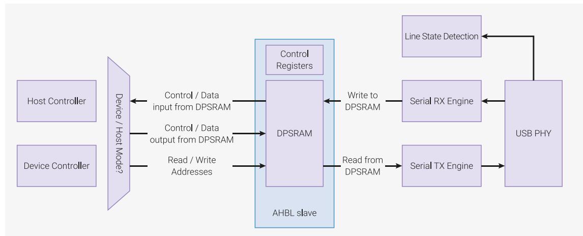
The USB controller is an area efficient design that muxes a device controller or host controller onto a common set of components. Each component is detailed below.
4.1.2.3. USB PHY
The USB PHY provides the electrical interface between the USB DP and DM pins and the digital logic of the controller. The DP and DM pins are a differential pair, meaning the values are always the inverse of each other, except to encode a specific line state ( SE0 , etc). The USB PHY drives the DP and DM pins to transmit data, as well as performing a differential receive of any incoming data. The USB PHY provides both single-ended and differential receive data to the line state detection module.
The USB PHY has built in pull-up and pull-down resistors. If the controller is acting as a Full Speed device then the DP pin is pulled up to indicate to the host that a Full Speed device has been connected. In host mode, a weak pull down is applied to DP and DM so that the lines are pulled to a logical zero until the device pulls up DP for Full Speed or DM for Low Speed.
4.1.2.4. Line state detection
The [2] defines several line states (Bus Reset, Connected, Suspend, Resume, Data 1, Data 0, etc) that need to be detected. The line state detection module has several state machines to detect these states and signal events to the other hardware components. There is no shared clock signal in USB, so the RX data must be sampled by an internal clock. The maximum data rate of USB Full Speed is 12Mbps. The RX data is sampled at 48MHz, giving 4 clock cycles to capture and filter the bus state. The line state detection module distributes the filtered RX data to the Serial RX Engine.
4.1.2.5. Serial RX Engine
The serial receive engine decodes receive data captured by the line state detection module. It produces the following information:
- • The PID of the incoming data packet
- • The device address for the incoming data
- • The device endpoint for the incoming data
- • Data bytes
The serial receive engine also detects errors in RX data by performing a CRC check on the incoming data. Any errors are signalled to the other hardware blocks and can raise an interrupt.
i NOTE
If you disconnect the USB cable during a packet in either host or device mode you will see errors raised by the hardware. Your software will need to take this scenario into account if you enable error interrupts.
4.1.2.6. Serial TX Engine
The serial transmit engine is a mirror of the serial receive engine. It is connected to the currently active controller (either device or host). It creates TOKEN and DATA packets, including calculating the CRC, and transmits them on the bus.
4.1.2.7. DPSRAM
The USB controller has 4kB (4096 bytes) of DPSRAM (Dual Port SRAM). The DPSRAM is used to store control registers and data buffers. The DPSRAM is accessible as a 32-bit wide memory at address 0 of the USB controller ( 0x50100000 ).
The DPSRAM has the following characteristics, which are different to most registers on RP2040:
- • Supports 8/16/32-bit accesses. Registers typically support 32-bit accesses only
- • The DPSRAM does not support set / clear aliases. RP2040 registers typically support these
Data Buffers are typically 64 bytes long as this is the max normal packet size for most FS packets. For Isochronous endpoints a maximum buffer size of 1023 bytes is supported. For other packet types the maximum size is 64 bytes per buffer.
4.1.2.7.1. Concurrent access
The DPSRAM in the USB controller should be considered asynchronous and not atomic. It is a dual port SRAM which means the processor has a port to read/write the memory and the USB controller also has a port to read/write the memory. This means that both the processor and the USB controller can access the same memory address at the same time. One could be writing and one could be reading. It is possible to get inconsistent data if the controller is reading the memory while the processor is writing the memory. Care must be taken to avoid this scenario.
The AVAILABLE bit in the buffer control register is used to indicate who has ownership of a buffer. This bit should be set to 1 by the processor to give the controller ownership of the buffer. The controller will set the bit back to 0 when it has used the buffer. The AVAILABLE bit should be set separately to the rest of the data in the buffer control register, so that the rest of the data in the buffer control register is accurate when the AVAILABLE bit is set.
This is necessary because the processor clock clk_sys can be running several times faster than the clk_usb clock. Therefore clk_sys can update the data during a read by the USB controller on a slower clock. The correct process is:
- • Write buffer information (length, etc.) to buffer control register
- •
nopfor someclk_syscycles to ensure that at least oneclk_usbcycle has passed. For example ifclk_syswas running at 125MHz andclk_usbwas running at 48MHz then 125/48 rounded up would be 3nopinstructions - • Set
AVAILABLEbit
If
clk_sys
and
clk_usb
are running at the same frequency then it is not necessary to set the
AVAILABLE
bit separately.
i NOTE
When the controller is writing status back to the DPSRAM it does a 16 bit write to the lower 2 bytes for buffer 0 and the upper 2 bytes for buffer 1. Therefore, if using double buffered mode, it is safest to treat the buffer control register as two 16 bit registers when updating it in software.
4.1.2.7.2. Layout
Addresses
0x0-0xff
are used for control registers containing configuration data. The remaining space, addresses
0x100-0xffff
(3840 bytes) can be used for data buffers. The controller has control registers that start at address
0x10000
.
The memory layout is different depending on if the controller is in Device or Host mode. In device mode, there are multiple endpoints a host can access so there must be endpoint control and buffer control registers for each endpoint. In host mode, the host software running on the processor is deciding which endpoints and which devices to access, so there only needs to be one set of endpoint control and buffer control registers. As well as software driven transfers, the host controller can poll up to 15 interrupt endpoints and has a register for each of these interrupt endpoints.
Table 394. DPSRAM layout
| Offset | Device Function | Host Function |
|---|---|---|
| 0x0 | Setup packet (8 bytes) | |
| 0x8 | EP1 in control | Interrupt endpoint control 1 |
| 0xc | EP1 out control | Spare |
| 0x10 | EP2 in control | Interrupt endpoint control 2 |
| 0x14 | EP2 out control | Spare |
| 0x18 | EP3 in control | Interrupt endpoint control 3 |
| 0x1c | EP3 out control | Spare |
| 0x20 | EP4 in control | Interrupt endpoint control 4 |
| 0x24 | EP4 out control | Spare |
| 0x28 | EP5 in control | Interrupt endpoint control 5 |
| 0x2c | EP5 out control | Spare |
| 0x30 | EP6 in control | Interrupt endpoint control 6 |
| 0x34 | EP6 out control | Spare |
| 0x38 | EP7 in control | Interrupt endpoint control 7 |
| 0x3c | EP7 out control | Spare |
| 0x40 | EP8 in control | Interrupt endpoint control 8 |
| 0x44 | EP8 out control | Spare |
| 0x48 | EP9 in control | Interrupt endpoint control 9 |
| 0x4c | EP9 out control | Spare |
| 0x50 | EP10 in control | Interrupt endpoint control 10 |
| 0x54 | EP10 out control | Spare |
| Offset | Device Function | Host Function |
|---|---|---|
| 0x58 | EP11 in control | Interrupt endpoint control 11 |
| 0x5c | EP11 out control | Spare |
| 0x60 | EP12 in control | Interrupt endpoint control 12 |
| 0x64 | EP12 out control | Spare |
| 0x68 | EP13 in control | Interrupt endpoint control 13 |
| 0x6c | EP13 out control | Spare |
| 0x70 | EP14 in control | Interrupt endpoint control 14 |
| 0x74 | EP14 out control | Spare |
| 0x78 | EP15 in control | Interrupt endpoint control 15 |
| 0x7c | EP15 out control | Spare |
| 0x80 | EP0 in buffer control | EPx buffer control |
| 0x84 | EP0 out buffer control | Spare |
| 0x88 | EP1 in buffer control | Interrupt endpoint buffer control 1 |
| 0x8c | EP1 out buffer control | Spare |
| 0x90 | EP2 in buffer control | Interrupt endpoint buffer control 2 |
| 0x94 | EP2 out buffer control | Spare |
| 0x98 | EP3 in buffer control | Interrupt endpoint buffer control 3 |
| 0x9c | EP3 out buffer control | Spare |
| 0xa0 | EP4 in buffer control | Interrupt endpoint buffer control 4 |
| 0xa4 | EP4 out buffer control | Spare |
| 0xa8 | EP5 in buffer control | Interrupt endpoint buffer control 5 |
| 0xac | EP5 out buffer control | Spare |
| 0xb0 | EP6 in buffer control | Interrupt endpoint buffer control 6 |
| 0xb4 | EP6 out buffer control | Spare |
| 0xb8 | EP7 in buffer control | Interrupt endpoint buffer control 7 |
| 0xbc | EP7 out buffer control | Spare |
| 0xc0 | EP8 in buffer control | Interrupt endpoint buffer control 8 |
| 0xc4 | EP8 out buffer control | Spare |
| 0xc8 | EP9 in buffer control | Interrupt endpoint buffer control 9 |
| 0xcc | EP9 out buffer control | Spare |
| 0xd0 | EP10 in buffer control | Interrupt endpoint buffer control 10 |
| 0xd4 | EP10 out buffer control | Spare |
| 0xd8 | EP11 in buffer control | Interrupt endpoint buffer control 11 |
| 0xdc | EP11 out buffer control | Spare |
| 0xe0 | EP12 in buffer control | Interrupt endpoint buffer control 12 |
| 0xe4 | EP12 out buffer control | Spare |
| clk_sys_busfabric clk_sys_clocks WAKE_EN registers to the • • • stop external clocks Interval Register | SLEEP_EN when the chip is inactive. If the user has not configured the stop unused clock sources such as the PLLs and Crystal Oscillator reduce the frequencies of generated clocks by increasing the clock divisors For maximum power saving when the chip is inactive, the user should consider DORMANT (see test interval. The interval is defined by counting cycles of The user can pick between accuracy and test time using the Test Interval | registers. The intention is to reduce power consumed in the clock distribution networks WAKE_EN and SLEEP_EN registers then system sleep will do Section 2.11.3) mode in clk_ref which must be driven either from XOSC or from a FC0_INTERVAL register. Table 206 shows the trade off. Accuracy |
|---|---|---|
| Offset | Device Function | Host Function |
| 0xe8 | EP13 in buffer control | Interrupt endpoint buffer control 13 |
| 0xec | EP13 out buffer control | Spare |
| 0xf0 | EP14 in buffer control | Interrupt endpoint buffer control 14 |
| 0xf4 | EP14 out buffer control | Spare |
| 0xf8 | EP15 in buffer control | Interrupt endpoint buffer control 15 |
| 0xfc | EP15 out buffer control | Spare |
| 0x100 | EP0 buffer 0 (shared between in and out) | EPx control |
| 0x140 | Optional EP0 buffer 1 | Spare |
| 0x180 0x180 | Data buffers Data buffers | |
| endpoint control register for EP0. Its buffers begin at | 0x100 . All other endpoints can have either single or dual buffers | |
| controls for EP0 come from Table 395. Endpoint Bit(s) control register layout | SIE_CTRL. Device Function | Host Function |
| 31 | Endpoint Enable Endpoint Enable | |
| 30 | Single buffered (64 bytes) = 0, Double buffered (64 bytes x 2) = 1 Single buffered (64 bytes) = 0, Double buffered (64 bytes x 2) = 1 | |
| 29 | Enable Interrupt for every transferred buffer Enable Interrupt for every transferred buffer | |
| 28 | Enable Interrupt for every 2 transferred buffers (valid for double buffered only) | |
| 27:26 27:26 | Endpoint Type: Control = 0, ISO = 1, Bulk = 2, Interrupt = 3 Endpoint Type: Control = 0, ISO = 1, Bulk = 2, Interrupt = 3 | |
| 25:18 | N/A | The interval the host controller should poll this endpoint. Only applicable for interrupt |
| 17 | Interrupt on Stall Interrupt on Stall | |
| 16 | Interrupt on NAK | value of 9 would poll the endpoint every 10ms. |
| 15:6 15:6 | Address base offset in DPSRAM of data buffer(s) Address base offset in DPSRAM of data buffer(s) |
4.1.2.7.3. Endpoint control register
The endpoint control register is used to configure an endpoint. It contains:
- • The endpoint type
- • The base address of its data buffer, or data buffers if double buffered
- • Interrupts events on the endpoint should trigger
A device must support Endpoint 0 so that it can reply to SETUP packets and be enumerated. As a result, there is no endpoint control register for EP0. Its buffers begin at
0x100
. All other endpoints can have either single or dual buffers and are mapped at the base address programmed. As EP0 has no endpoint control register, the interrupt enable controls for EP0 come from
SIE_CTRL
.
Table 395. Endpoint control register layout
i NOTE
The data buffer base address must be 64-byte aligned as bits 0-5 are ignored
4.1.2.7.4. Buffer control register
The buffer control register contains information about the state of the data buffers for that endpoint. It is shared between the processor and the controller. If the endpoint is configured to be single buffered, only the first half (bits 0-15) of the buffer are used.
If double buffering, the buffer select starts at buffer 0. From then on, the buffer select flips between buffer 0 and 1 unless the "reset buffer select" bit is set (which resets the buffer select to buffer 0). The value of the buffer select is internal to the controller and not accessible by the processor.
For host interrupt and isochronous packets on EPx, the buffer full bit will be set on completion even if the transfer was unsuccessful. The error bits in the SIE_STATUS register can be read to determine the error.
Table 396. Buffer control register layout
| Bit(s) | Function |
|---|---|
| 31 | Buffer 1 full. Should be set to 1 by the processor for an IN transaction and 0 for an OUT transaction. The controller sets this to 1 for an OUT transaction because it has filled the buffer. The controller sets it to 0 for an IN transaction because it has emptied the buffer. Only valid for double buffered |
| 30 | Last buffer of transfer for buffer 1 - only valid for double buffered |
| 29 | Data PID for buffer 1 - DATA0 = 0, DATA1 = 1 - only valid for double buffered |
| 27:28 | Double buffer offset for Isochronous mode (0 = 128, 1 = 256, 2 = 512, 3 = 1024) |
| 26 | Buffer 1 available. Whether the buffer can be used by the controller for a transfer. The processor sets this to 1 when the buffer is configured. The controller sets to 0 when it has used the buffer. i.e. has sent the data to the host for an IN transaction or has filled the buffer with data from the host for an OUT transaction. Only valid for double buffered. |
| 25:16 | Buffer 1 transfer length - only valid for double buffered |
| 15 | Buffer 0 full. Should be set to 1 by the processor for an IN transaction and 0 for an OUT transaction. The controller sets this to 1 for an OUT transaction because it has filled the buffer. The controller sets it to 0 for an IN transaction because it has emptied the buffer. |
| 14 | Last buffer of transfer for buffer 0 |
| 13 | Data PID for buffer 0 - DATA0 = 0, DATA1 = 1 |
| 12 | Reset buffer select to buffer 0 - cleared at end of transfer. For DEVICE ONLY |
| 11 | Send STALL for device, STALL received for host |
| 10 | Buffer 0 available. Whether the buffer can be used by the controller for a transfer. The processor sets this to 1 when the buffer is configured. The controller sets to 0 when it has used the buffer. i.e. has sent the data to the host for an IN transaction or has filled the buffer with data from the host for an OUT transaction. |
| 9:0 | Buffer 0 transfer length |
⚠ WARNING
If running
clk_sys
and
clk_usb
at different speeds, the available and stall bits should be set after the other data in the buffer control register. Otherwise the controller may initiate a transaction with data from a previous packet. That is to say, the controller could see the available bit set but get the data pid or length from the previous packet.
4.1.2.8. Device Controller
This section details how the device controller operates when it receives various packet types from the host.
4.1.2.8.1. SETUP
The device controller MUST always accept a setup packet from the host. That is why the first 8 bytes of the DPSRAM has dedicated space for the setup packet.
The [2] states that receiving a setup packet also clears any stall bits on EP0. For this reason, the stall bits for EP0 are gated with two bits in the
EP_STALL_ARM
register. These bits are cleared when a setup packet is received. This means that to send a stall on EP0, you have to set both the stall bit in the buffer control register, and the appropriate bit in
EP_STALL_ARM
.
Barring any errors, the setup packet will be put into the setup packet buffer at DPSRAM offset
0x0
. The device controller will then reply with an ACK.
Finally,
SIE_STATUS.SETUP_REC
is set to indicate that a setup packet has been received. This will trigger an interrupt if the programmer has enabled the
SETUP_REC
interrupt (see
INTE
).
4.1.2.8.2. IN
From the device's point of view, an IN transfer means transferring data INTO the host. When an IN token is received from the host the request is handled as follows:
TOKEN phase:
- • If
STALL
is set in the buffer control register (and if EP0, the appropriate
EP_STALL_ARMbit is set) then send a STALL response and go back to idle. - • If AVAILABLE and FULL bits are set in buffer control move to the phase
- • Otherwise send NAK unless this is an Isochronous endpoint, in which case go to idle.
DATA phase:
- • Send DATA. If Isochronous go to idle. Otherwise move to ACK phase.
ACK phase:
- • Wait for ACK packet from host. If there is a timeout then raise a timeout error. If ACK is received then the packet is done, so move to status phase.
STATUS phase:
- • If this was the last buffer in the transfer (i.e. if the
LAST_BUFFERbit in the buffer control register was set), setSIE_STATUS.TRANS_COMPLETE. - • If the endpoint is double buffered, flip the buffer select to the other buffer.
- • Set a bit in
BUFF_STATUSto indicate the buffer is done. When handling this event, the programmer should readBUFF_CPU_SHOULD_HANDLEto see if it is buffer 0 or buffer 1 that is finished. If the endpoint is double buffered it is possible to have both buffers done. The clearedBUFF_STATUSbit will be set again, andBUFF_CPU_SHOULD_HANDLEwill change in this instance. - • Update status in the appropriate half of the buffer control register: length, pid, and last_buff are set. Everything else is written to zero.
If a NAK gets sent to the host the host will retry again later.
4.1.2.8.3. OUT
When an OUT token is received from the host, the request is handled as follows:
TOKEN phase:
- • Is the DATA pid what is specified in the buffer control register? If not raise
SIE_STATUS.DATA_SEQ_ERROR. (The data pid for an Isochronous endpoint is not checked because Isochronous data is always sent with a DATA0 pid.) - • Is the AVAILABLE bit set and the FULL bit unset. If so go to the data phase, unless the STALL bit is set in which case the device controller will reply with a STALL .
DATA phase:
- • Store received data in buffer. If Isochronous go to STATUS phase. Otherwise go to ACK phase.
ACK phase:
- • Send ACK. Go to STATUS phase.
STATUS phase:
See status phase from Section 4.1.2.8.2 . The only difference is that the FULL bit is set in the buffer control register to indicate that data has been received whereas in the IN case the FULL bit is cleared to indicate that data has been sent.
4.1.2.8.4. Suspend and Resume
The USB device controller supports both suspend and resume, as well as remote resume (triggered with SIE_CTRL.RESUME ), where the device initiates the resume. There is an interrupt / status bit in SIE_STATUS . It is not necessary to enable the suspend and resume interrupts, as most devices do not need to care about suspend and resume.
The device goes into suspend when it does not see any start of frame packets (transmitted every 1ms) from the host.
i NOTE
If you enable the suspend interrupt, it is likely you will see a suspend interrupt when the device is first connected but the bus is idle. The bus can be idle for a few ms before the host begins sending start of frame packets. You will also see a suspend interrupt when the device is disconnected if you do not have a VBUS detect circuit connected. This is because without VBUS detection, it is impossible to tell the difference between being disconnected and suspended.
4.1.2.8.5. Errata
There are two hardware issues with the device controller, both of which have software workarounds on RP2040B0, RP2040B1, and are fixed in hardware on RP2040B2. See RP2040-E2 and RP2040-E5 for more information.
4.1.2.9. Host Controller
The host controller design is similar to the device controller. All transactions are started by the host, so the host is always dealing with transactions it has started. For this reason there is only one set of endpoint control / endpoint buffer control registers. There is also additional hardware to poll interrupt endpoints in the background when there are no software controlled transactions taking place.
The host needs to send keep-alive packets to the device every 1ms to keep the device from suspending. In Full Speed mode this is done by sending a SOF (start of frame) packet. In Low Speed mode, an EOP (end of packet) is sent. When setting up the controller, SIE_CTRL.KEEP_ALIVE_EN and SIE_CTRL.SOF_EN should be set to enable these packets.
Several bits in SIE_CTRL are used to begin a host transaction:
- • SEND_SETUP - Send a setup packet. This is typically used in conjunction with RECEIVE_TRANS so the setup packet will be sent followed by the additional data transaction expected from the device.
- • SEND_TRANS - This transfer is OUT from the host
- • RECEIVE_TRANS - This transfer is IN to the host
- • START_TRANS - Start the transfer - non-latching
- • STOP_TRANS - Stop the current transfer - non-latching
- • PREAMBLE_ENABLE - Use this to send a packet to a Low Speed device on a Full Speed hub. This will send a PRE token packet before every packet the host sends (i.e. pre, token, pre, data, pre, ack).
- • SOF_SYNC - The SOF Sync bit is used to delay the transaction until after the next SOF. This is useful for interrupt and isochronous endpoints. The Host controller prevents a transaction of 64bytes from clashing with the SOF packets.
For longer Isochronous packet the software is responsible for preventing a collision by using the SOF Sync bit and limiting the number of packets sent in one frame. If a transaction is set up with multiple packets the SOF Sync bit only applies to the first packet.
⚠ WARNING
The
START_TRANS
bit is synchronised separately to other control bits in the
SIE_CTRL
register. The
START_TRANS
bit should be set separately to the rest of the data in the
SIE_CTRL
register, so that the register contents are stable when the controller is prompted to start a transfer. This is necessary because the processor clock
clk_sys
can be asynchronous to the
clk_usb
clock.
- • Write fields in
SIE_CTRLapart fromSTART_TRANS - •
nopfor someclk_syscycles to ensure that at least twoclk_usbcycles have passed. For example ifclk_syswas running at 125MHz andclk_usbwas running at 48MHz then 125/48 rounded up would be 6nopinstructions - • Set the
START_TRANSbit.
4.1.2.9.1. SETUP
The
SETUP
packet sent from the host always comes from the dedicated 8 bytes of space at offset
0x0
of the DPSRAM. Like the device controller, there are no control registers associated with the setup packet. The parameters are hard coded and loaded into the hardware when you write to
START_TRANS
with the
SEND_SETUP
bit set. Once the setup packet has been sent, the host state machine will wait for an
ACK
from the device. If there is a timeout then an
RX_TIMEOUT
error will be raised. If the
SEND_TRANS
bit is set then the host state machine will move to the
OUT
phase. Most commonly the
SEND_SETUP
packet is used in conjunction with the
RECEIVE_TRANS
bit and will therefore move to the
IN
phase after sending a setup packet.
4.1.2.9.2. IN
An
IN
transfer is triggered with the
RECEIVE_TRANS
bit set when the
START_TRANS
bit is set. This may be preceded by a
SETUP
packet being sent if the
SEND_SETUP
bit was set.
CONTROL phase:
- • Read
EPx control
register located at
0x80to get the endpoint information:- ◦ Are we double buffered?
- ◦ What interrupts to enable
- ◦ Base address of the data buffer, or data buffers if in double buffered mode
- ◦ Endpoint type
- • Read
EPx buffer control
register at
0x100to get the endpoint buffer information such as transfer length and data pid. The host state machine still checks for the presence of theAVAILABLEbit, so this needs to be set andFULLneeds to be unset. The transaction will not happen until this is the case.
TOKEN phase:
- • Send the
INtoken packet to the device. The target device address and endpoint come from theADDR_ENDPregister.
DATA phase:
- • Receive the first data packet from the device. Raise RX timeout error if the device doesn't reply. Raise DATA SEQ ERROR if the data packet has wrong DATA PID.
ACK phase:
- • Send ACK to device
STATUS phase:
- • Set BUFF_STATUS bit and update buffer control register. Will set FULL , LAST_BUFF if applicable, DATA_PID , WR_LEN . TRANS_COMPLETE will be set if this is the last buffer in the transfer.
CONTROL phase (pt 2):
- • The host state machine will keep performing IN transactions until LAST_BUFF is seen in the buffer_control register. If the host is in double buffered mode then the host controller will toggle between BUF0 and BUF1 sections of the buffer control register. Otherwise it will keep reading the buffer control register for buffer 0 and wait for the FULL to be unset and AVAILABLE to be set before starting the next IN transaction (i.e. wait in the control phase). The device can send a zero length packet to the host to indicate that it has no more data. In which case the host state machine will stop listening for more data regardless of if the LAST_BUFF flag was set or not. The host software can tell this has happened because BUFF_DONE will be set with a data length of 0 in the buffer control register.
⚠ WARNING
The USB host controller has a bug ( RP2040-E4 ) that means the status written back to the buffer control register can appear in the wrong half of the register. Bits 0-15 are for buffer 0, and bits 16-31 are for buffer 1. The host controller has a buffer selector that is flipped after each transfer is complete. This buffer selector is incorrectly used when writing status information back to the buffer control register even in single buffered mode. The buffer selector is not used when reading the buffer control register. The implication of this is that host software needs to keep track of the buffer selector and shift the buffer control register to the right by 16 bits if the buffer selector is 1.
For more information, see RP2040-E4 .
4.1.2.9.3. OUT
An OUT transfer is triggered with the SEND_TRANS bit set when the START_TRANS bit is set. This may be preceded by a SETUP packet being sent if the SEND_SETUP bit was set.
CONTROL phase:
- • Read EPx control to get endpoint information (same as Section 4.1.2.9.2 )
- • Read EPx buffer control to get the transfer length, data pid. AVAILABLE and FULL must be set for the transfer to start.
TOKEN phase
- • Send OUT packet to the device. The target device address and endpoint come from the ADDR_ENDP register.
DATA phase:
- • Send the first data packet to the device. If the endpoint type is Isochronous then there is no ACK phase so the host controller will go straight to status phase. If
ACK
received then go to status phase. Otherwise:
- ◦ If no reply is received then raise SIE_STATUS.RX_TIMEOUT .
- ◦ If NAK received raise SIE_STATUS.NAK_REC and send the data packet again.
- ◦ If STALL received then raise SIE_STATUS.STALL_REC and go to idle.
STATUS phase:
- • Set BUFF_STATUS bit and update buffer control register. FULL will be set to 0. TRANS_COMPLETE will be set if this is the last buffer in the transfer.
⚠ WARNING
The bug mentioned above ( RP2040-E4 ) in the IN section also applies to the OUT section.
CONTROL phase (pt 2):
If this isn't the last buffer in the transfer then wait for FULL and AVAILABLE to be set in the EPx buffer control register again.
4.1.2.9.4. Interrupt Endpoints
The host controller can poll interrupt endpoints on many devices (up to a maximum of 15 endpoints). To enable these, the programmer must:
- • Pick the next free interrupt endpoint slot on the host controller (starting at 1, to a maximum of 15)
- • Program the appropriate endpoint control register and buffer control register like you would with a normal IN or OUT transfer. Note that interrupt endpoints are only single buffered so the BUF1 part of the buffer control register is invalid.
- • Set the address and endpoint of the device in the appropriate ADDR_ENDP register ( ADDR_ENDP1 to ADDR_ENDP15 ). The preamble bit should be set if the device is Low Speed but attached to a Full Speed hub. The endpoint direction bit should also be set.
- • Set the interrupt endpoint active bit in INT_EP_CTRL (i.e. set bit 1 to 15 of that register)
Typically an interrupt endpoint will be an IN transfer. For example, a USB hub would be polled to see if the state of any of its ports have changed. If there is no change the hub will reply with a NAK to the controller and nothing will happen. Similarly, a mouse will reply with a NAK unless the mouse has been moved since the last time the interrupt endpoint was polled.
Interrupt endpoints are polled by the controller once a SOF packet has been sent by the host controller.
The controller loops from 1 to 15 and will attempt to poll any interrupt endpoint with the EP_ACTIVE bit set to 1 in INT_EP_CTRL . The controller will then read the endpoint control register, and buffer control register to see if there is an available buffer (i.e. FULL + AVAILABLE if an OUT transfer and NOT FULL + AVAILABLE for an IN transfer). If not, the controller will move onto the next interrupt endpoint slot.
If there is an available buffer, then the transfer is dealt with the same as a normal IN or OUT transfer and the BUFF_DONE flag in BUFF_STATUS will be set when the interrupt endpoint has a valid buffer. BUFF_CPU_SHOULD_HANDLE is invalid for interrupt endpoints as there is only a single buffer that can ever be done ( RP2040-E3 ).
4.1.2.10. VBUS Control
The USB controller can be connected up to GPIO pins (see Section 2.19 ) for the purpose of VBUS control:
- • VBUS enable, used to enable VBUS in host mode. VBUS enable is set in SIE_CTRL
- • VBUS detect, used to detect that VBUS is present in device mode. VBUS detect is a bit in SIE_STATUS and can also raise a VBUS_DETECT interrupt (enabled in INTE )
- • VBUS overcurrent, used to detect an overcurrent event. Applicable to both device and host. VBUS overcurrent is a bit in SIE_STATUS .
It is not necessary to connect up any of these pins to GPIO. The host can permanently supply VBUS and detect a device being connected when either the DP or DM pin is pulled high. VBUS detect can be forced in USB_PWR .
4.1.3. Programmer's Model
4.1.3.1. TinyUSB
The RP2040 TinyUSB port should be considered as the reference implementation for this USB controller. This port can be found in:
https://github.com/hathach/tinyusb/blob/master/src/portable/raspberrypi/rp2040/dcd_rp2040.c
https://github.com/hathach/tinyusb/blob/master/src/portable/raspberrypi/rp2040/hcd_rp2040.c
https://github.com/hathach/tinyusb/blob/master/src/portable/raspberrypi/rp2040/rp2040_usb.h
4.1.3.2. Standalone device example
A standalone USB device example,
dev_lowlevel
, makes it easier to understand how to interact with the USB controller without needing to understand the TinyUSB abstractions. In addition to endpoint 0, the standalone device has two bulk endpoints: EP1 OUT and EP2 IN. The device is designed to send whatever data it receives on EP1 to EP2. The example comes with a small Python script that writes "Hello World" into EP1 and checks that it is correctly received on EP2.
The code included in this section will walk you through setting up to the USB device controller to receive a setup packet, and then respond to the setup packet.
Figure 58. USB analyser trace of the
dev_lowlevel
USB device example. The control transfers are the device enumeration. The first bulk OUT (out from the host) transfer, highlighted in blue, is the host sending "Hello World" to the device. The second bulk transfer IN (in to the host), is the device returning "Hello World" to the host.
| Ch0 | Packet 522 | H | Reset | 15.006 ms | ||||
| Transfer 0 | F | Control | ADDR 0 | ENDP 0 | bRequest GET_DESCRIPTOR | wValue DEVICE type | wIndex 0x0000 | Descriptors |
| Transfer 1 | S | Control | ADDR 7 | ENDP 0 | bRequest SET_ADDRESS | wValue New address 7 | wIndex 0x0000 | wLength 0 |
| Transfer 2 | F | Control | ADDR 7 | ENDP 0 | bRequest GET_DESCRIPTOR | wValue DEVICE type | wIndex 0x0000 | Descriptors |
| Transfer 3 | S | Control | ADDR 7 | ENDP 0 | bRequest GET_DESCRIPTOR | wValue CONFIGURATION type, Index 0 | wIndex 0x0000 | Descriptors |
| Transfer 4 | F | Control | ADDR 7 | ENDP 0 | bRequest GET_DESCRIPTOR | wValue CONFIGURATION type, Index 0 | wIndex 0x0000 | 4 Descriptors |
| Transfer 5 | S | Control | ADDR 7 | ENDP 0 | bRequest GET_DESCRIPTOR | wValue STRING type, LANGID codes requested | wIndex Language ID 0x0000 | Lang Supported |
| Transfer 6 | F | Control | ADDR 7 | ENDP 0 | bRequest GET_DESCRIPTOR | wValue STRING type, Index 2 | wIndex Language ID 0x0409 | Pico Test Device |
| Transfer 7 | S | Control | ADDR 7 | ENDP 0 | bRequest GET_DESCRIPTOR | wValue STRING type, Index 1 | wIndex Language ID 0x0409 | Raspberry Pi |
| Transfer 8 | F | Control | ADDR 7 | ENDP 0 | bRequest SET_CONFIGURATION | wValue New Configuration 1 | wIndex 0x0000 | wLength 0 |
| Transfer 9 | S | Bulk | ADDR 7 | ENDP 1 | Bytes Transferred | 12 | ||
| Transfer 10 | F | Bulk | ADDR 7 | ENDP 2 | Bytes Transferred | 12 | ||
4.1.3.2.1. Device controller initialisation
The following code initialises the USB device.
Pico Examples: https://github.com/raspberrypi/pico-examples/blob/master/usb/device/dev_lowlevel/dev_lowlevel.c Lines 183 - 217
183 void usb_device_init() {
184     // Reset usb controller
185     reset_unreset_block_num_wait_blocking(RESET_USBCTRL);
186
187     // Clear any previous state in dpram just in case
188     memset(usb_dpram, 0, sizeof(*usb_dpram)); ①
189
190     // Enable USB interrupt at processor
191     irq_set_enabled(USBCTRL_IRQ, true);
192
193     // Mux the controller to the onboard usb phy
194     usb_hw->muxing = USB_USB_MUXING_TO_PHY_BITS | USB_USB_MUXING_SOFTCON_BITS;
195
196     // Force VBUS detect so the device thinks it is plugged into a host
197     usb_hw->pwr = USB_USB_PWR_VBUS_DETECT_BITS | USB_USB_PWR_VBUS_DETECT_OVERRIDE_EN_BITS;
198
199     // Enable the USB controller in device mode.
200     usb_hw->main_ctrl = USB_MAIN_CTRL_CONTROLLER_EN_BITS;
201
202     // Enable an interrupt per EP0 transaction
203     usb_hw->sie_ctrl = USB_SIE_CTRL_EP0_INT_1BUF_BITS; ②
204
205     // Enable interrupts for when a buffer is done, when the bus is reset,
206     // and when a setup packet is received
207     usb_hw->inte = USB_INTS_BUFF_STATUS_BITS |
208                   USB_INTS_BUS_RESET_BITS |
209                   USB_INTS_SETUP_REQ_BITS;
210
211     // Set up endpoints (endpoint control registers)
212     // described by device configuration
213     usb_setup_endpoints();
214
215     // Present full speed device by enabling pull up on DP
216     usb_hw_set->sie_ctrl = USB_SIE_CTRL_PULLUP_EN_BITS;
217 }
4.1.3.2.2. Configuring the endpoint control registers for EP1 and EP2
The function
usb_configure_endpoints
loops through each endpoint defined in the device configuration (including EP0 in and EP0 out, which don't have an endpoint control register defined) and calls the
usb_configure_endpoint
function. This sets up the endpoint control register for that endpoint:
Pico Examples: https://github.com/raspberrypi/pico-examples/blob/master/usb/device/dev_lowlevel/dev_lowlevel.c Lines 149 - 164
149 void usb_setup_endpoint(const struct usb_endpoint_configuration *ep) {
150     printf("Set up endpoint 0x%x with buffer address 0x%p\n", ep->descriptor-
151           >bEndpointAddress, ep->data_buffer);
152
153     // EP0 doesn't have one so return if that is the case
154     if (!ep->endpoint_control) {
155         return;
156     }
157
158     // Get the data buffer as an offset of the USB controller's DPRAM
159     uint32_t dpram_offset = usb_buffer_offset(ep->data_buffer);
160     uint32_t reg = EP_CTRL_ENABLE_BITS
161                 | EP_CTRL_INTERRUPT_PER_BUFFER
162                 | (ep->descriptor->bmAttributes << EP_CTRL_BUFFER_TYPE_LSB)
163                 | dpram_offset;
164     *ep->endpoint_control = reg;
165 }
4.1.3.2.3. Receiving a setup packet
An interrupt is raised when a setup packet is received, so the interrupt handler must handle this event:
Pico Examples: https://github.com/raspberrypi/pico-examples/blob/master/usb/device/dev_lowlevel/dev_lowlevel.c Lines 494 - 504
494 void isr_usbctrl(void) {
495     // USB interrupt handler
496     uint32_t status = usb_hw->ints;
497     uint32_t handled = 0;
498
499     // Setup packet received
500     if (status & USB_INTS_SETUP_REQ_BITS) {
501         handled |= USB_INTS_SETUP_REQ_BITS;
502         usb_hw_clear->sie_status = USB_SIE_STATUS_SETUP_REC_BITS;
503         usb_handle_setup_packet();
504     }
The setup packet gets written to the first 8 bytes of the USB ram, so the setup packet handler casts that area of memory to
struct usb_setup_packet *
.
Pico Examples: https://github.com/raspberrypi/pico-examples/blob/master/usb/device/dev_lowlevel/dev_lowlevel.c Lines 383 - 427
383 void usb_handle_setup_packet(void) {
384     volatile struct usb_setup_packet *pkt = (volatile struct usb_setup_packet *) &usb_dpram
->setup_packet;
385     uint8_t req_direction = pkt->bmRequestType;
386     uint8_t req = pkt->bRequest;
387
388     // Reset PID to 1 for EP0 IN
389     usb_get_endpoint_configuration(EP0_IN_ADDR)->next_pid = 1u;
390
391     if (req_direction == USB_DIR_OUT) {
392         if (req == USB_REQUEST_SET_ADDRESS) {
393             usb_set_device_address(pkt);
394         } else if (req == USB_REQUEST_SET_CONFIGURATION) {
395             usb_set_device_configuration(pkt);
396         } else {
397             usb_acknowledge_out_request();
398             printf("Other OUT request (0x%x)\r\n", pkt->bRequest);
399         }
400     } else if (req_direction == USB_DIR_IN) {
401         if (req == USB_REQUEST_GET_DESCRIPTOR) {
402             uint16_t descriptor_type = pkt->wValue >> 8;
403
404             switch (descriptor_type) {
405                 case USB_DT_DEVICE:
406                     usb_handle_device_descriptor(pkt);
407                     printf("GET DEVICE DESCRIPTOR\r\n");
408                     break;
409
410                 case USB_DT_CONFIG:
411                     usb_handle_config_descriptor(pkt);
412                     printf("GET CONFIG DESCRIPTOR\r\n");
413                     break;
414
415                 case USB_DT_STRING:
416                     usb_handle_string_descriptor(pkt);
417                     printf("GET STRING DESCRIPTOR\r\n");
418                     break;
419
420                 default:
421                     printf("Unhandled GET_DESCRIPTOR type 0x%x\r\n", descriptor_type);
422             }
423         } else {
424             printf("Other IN request (0x%x)\r\n", pkt->bRequest);
425     }
426 }
427 }
4.1.3.2.4. Replying to a setup packet on EP0 IN
The first thing a host will request is the device descriptor, the following code handles that setup request.
Pico Examples: https://github.com/raspberrypi/pico-examples/blob/master/usb/device/dev_lowlevel/dev_lowlevel.c Lines 266 - 273
266 void usb_handle_device_descriptor(volatile struct usb_setup_packet *pkt) {
267     const struct usb_device_descriptor *d = dev_config.device_descriptor;
268     // EP0 in
269     struct usb_endpoint_configuration *ep = usb_get_endpoint_configuration(EP0_IN_ADDR);
270     // Always respond with pid 1
271     ep->next_pid = 1;
272     usb_start_transfer(ep, (uint8_t *) d, MIN(sizeof(struct usb_device_descriptor), pkt->wLength));
273 }
The
usb_start_transfer
function copies the data to send into the appropriate hardware buffer, and configures the buffer control register. Once the buffer control register has been written to, the device controller will respond to the host with the data. Before this point, the device will reply with a
NAK
.
Pico Examples: https://github.com/raspberrypi/pico-examples/blob/master/usb/device/dev_lowlevel/dev_lowlevel.c Lines 238 - 260
238 void usb_start_transfer(struct usb_endpoint_configuration *ep, uint8_t *buf, uint16_t len) {
239     // We are asserting that the length is <= 64 bytes for simplicity of the example.
240     // For multi packet transfers see the tinyusb port.
241     assert(len <= 64);
242
243     printf("Start transfer of len %d on ep addr 0x%x\n", len, ep->descriptor->bEndpointAddress);
244
245     // Prepare buffer control register value
246     uint32_t val = len | USB_BUF_CTRL_AVAIL;
247
248     if (ep_is_tx(ep)) {
249         // Need to copy the data from the user buffer to the usb memory
250         memcpy((void *) ep->data_buffer, (void *) buf, len);
251         // Mark as full
252         val |= USB_BUF_CTRL_FULL;
253     }
254
255     // Set pid and flip for next transfer
256     val |= ep->next_pid ? USB_BUF_CTRL_DATA1_PID : USB_BUF_CTRL_DATA0_PID;
257     ep->next_pid ^= 1u;
258
259     *ep->buffer_control = val;
260 }
4.1.4. List of Registers
The USB registers start at a base address of
0x50110000
(defined as
USBCTRL_REGS_BASE
in SDK).
Table 397. List of USB registers
| Offset | Name | Info |
|---|---|---|
| 0x00 | ADDR_ENDP | Device address and endpoint control |
| 0x04 | ADDR_ENDP1 | Interrupt endpoint 1. Only valid for HOST mode. |
| 0x08 | ADDR_ENDP2 | Interrupt endpoint 2. Only valid for HOST mode. |
| 0x0c | ADDR_ENDP3 | Interrupt endpoint 3. Only valid for HOST mode. |
| 0x10 | ADDR_ENDP4 | Interrupt endpoint 4. Only valid for HOST mode. |
| 0x14 | ADDR_ENDP5 | Interrupt endpoint 5. Only valid for HOST mode. |
| 0x18 | ADDR_ENDP6 | Interrupt endpoint 6. Only valid for HOST mode. |
| 0x1c | ADDR_ENDP7 | Interrupt endpoint 7. Only valid for HOST mode. |
| 0x20 | ADDR_ENDP8 | Interrupt endpoint 8. Only valid for HOST mode. |
| 0x24 | ADDR_ENDP9 | Interrupt endpoint 9. Only valid for HOST mode. |
| 0x28 | ADDR_ENDP10 | Interrupt endpoint 10. Only valid for HOST mode. |
| 0x2c | ADDR_ENDP11 | Interrupt endpoint 11. Only valid for HOST mode. |
| 0x30 | ADDR_ENDP12 | Interrupt endpoint 12. Only valid for HOST mode. |
| 0x34 | ADDR_ENDP13 | Interrupt endpoint 13. Only valid for HOST mode. |
| 0x38 | ADDR_ENDP14 | Interrupt endpoint 14. Only valid for HOST mode. |
| 0x3c | ADDR_ENDP15 | Interrupt endpoint 15. Only valid for HOST mode. |
| 0x40 | MAIN_CTRL | Main control register |
| 0x44 | SOF_WR | Set the SOF (Start of Frame) frame number in the host controller. The SOF packet is sent every 1ms and the host will increment the frame number by 1 each time. |
| 0x48 | SOF_RD | Read the last SOF (Start of Frame) frame number seen. In device mode the last SOF received from the host. In host mode the last SOF sent by the host. |
| 0x4c | SIE_CTRL | SIE control register |
| 0x50 | SIE_STATUS | SIE status register |
| 0x54 | INT_EP_CTRL | interrupt endpoint control register |
| 0x58 | BUFF_STATUS | Buffer status register. A bit set here indicates that a buffer has completed on the endpoint (if the buffer interrupt is enabled). It is possible for 2 buffers to be completed, so clearing the buffer status bit may instantly re set it on the next clock cycle. |
| 0x5c | BUFF_CPU_SHOULD_HANDLE | Which of the double buffers should be handled. Only valid if using an interrupt per buffer (i.e. not per 2 buffers). Not valid for host interrupt endpoint polling because they are only single buffered. |
| 0x60 | EP_ABORT | Device only: Can be set to ignore the buffer control register for this endpoint in case you would like to revoke a buffer. A NAK will be sent for every access to the endpoint until this bit is cleared. A corresponding bit in EP_ABORT_DONE is set when it is safe to modify the buffer control register. |
| Offset | Name | Info |
|---|---|---|
| 0x64 | EP_ABORT_DONE | Device only: Used in conjunction with EP_ABORT . Set once an endpoint is idle so the programmer knows it is safe to modify the buffer control register. |
| 0x68 | EP_STALL_ARM | Device: this bit must be set in conjunction with the STALL bit in the buffer control register to send a STALL on EP0. The device controller clears these bits when a SETUP packet is received because the USB spec requires that a STALL condition is cleared when a SETUP packet is received. |
| 0x6c | NAK_POLL | Used by the host controller. Sets the wait time in microseconds before trying again if the device replies with a NAK. |
| 0x70 | EP_STATUS_STALL_NAK | Device: bits are set when the IRQ_ON_NAK or IRQ_ON_STALL bits are set. For EP0 this comes from SIE_CTRL . For all other endpoints it comes from the endpoint control register. |
| 0x74 | USB_MUXING | Where to connect the USB controller. Should be to_phy by default. |
| 0x78 | USB_PWR | Overrides for the power signals in the event that the VBUS signals are not hooked up to GPIO. Set the value of the override and then the override enable to switch over to the override value. |
| 0x7c | USBPHY_DIRECT | This register allows for direct control of the USB phy. Use in conjunction with usbphy_direct_override register to enable each override bit. |
| 0x80 | USBPHY_DIRECT_OVERRIDE | Override enable for each control in usbphy_direct |
| 0x84 | USBPHY_TRIM | Used to adjust trim values of USB phy pull down resistors. |
| 0x8c | INTR | Raw Interrupts |
| 0x90 | INTE | Interrupt Enable |
| 0x94 | INTF | Interrupt Force |
| 0x98 | INTS | Interrupt status after masking & forcing |
USB: ADDR_ENDP Register
Offset: 0x00
Description
Device address and endpoint control
Table 398.
ADDR_ENDP Register
| Bits | Description | Type | Reset |
|---|---|---|---|
| 31:20 | Reserved. | - | - |
| 19:16 | ENDPOINT: Device endpoint to send data to. Only valid for HOST mode. | RW | 0x0 |
| 15:7 | Reserved. | - | - |
| 6:0 | ADDRESS: In device mode, the address that the device should respond to. Set in response to a SET_ADDR setup packet from the host. In host mode set to the address of the device to communicate with. | RW | 0x00 |
USB: ADDR_ENDP1, ADDR_ENDP2, ..., ADDR_ENDP14, ADDR_ENDP15 Registers
Offsets: 0x04, 0x08, ..., 0x38, 0x3c
Description
Interrupt endpoint N . Only valid for HOST mode.
Table 399.
ADDR_ENDP1,
ADDR_ENDP2, ...,
ADDR_ENDP14,
ADDR_ENDP15
Registers
| Bits | Description | Type | Reset |
|---|---|---|---|
| 31:27 | Reserved. | - | - |
| 26 | INTEP_PREAMBLE: Interrupt EP requires preamble (is a low speed device on a full speed hub) | RW | 0x0 |
| 25 | INTEP_DIR: Direction of the interrupt endpoint. In=0, Out=1 | RW | 0x0 |
| 24:20 | Reserved. | - | - |
| 19:16 | ENDPOINT: Endpoint number of the interrupt endpoint | RW | 0x0 |
| 15:7 | Reserved. | - | - |
| 6:0 | ADDRESS: Device address | RW | 0x00 |
USB: MAIN_CTRL Register
Offset: 0x40
Description
Main control register
Table 400.
MAIN_CTRL Register
| Bits | Description | Type | Reset |
|---|---|---|---|
| 31 | SIM_TIMING: Reduced timings for simulation | RW | 0x0 |
| 30:2 | Reserved. | - | - |
| 1 | HOST_NDEVICE: Device mode = 0, Host mode = 1 | RW | 0x0 |
| 0 | CONTROLLER_EN: Enable controller | RW | 0x0 |
USB: SOF_WR Register
Offset: 0x44
Description
Set the SOF (Start of Frame) frame number in the host controller. The SOF packet is sent every 1ms and the host will increment the frame number by 1 each time.
Table 401. SOF_WR
Register
| Bits | Description | Type | Reset |
|---|---|---|---|
| 31:11 | Reserved. | - | - |
| 10:0 | COUNT | WF | 0x000 |
USB: SOF_RD Register
Offset: 0x48
Description
Read the last SOF (Start of Frame) frame number seen. In device mode the last SOF received from the host. In host mode the last SOF sent by the host.
Table 402. SOF_RD
Register
| Bits | Description | Type | Reset |
|---|---|---|---|
| 31:11 | Reserved. | - | - |
| Bits 14:10 9:5 4:0 Bits | Description SHIFT Description | MASK_MSB : The most-significant bit allowed to pass by the mask (inclusive) MASK_LSB : The least-significant bit allowed to pass by the mask (inclusive) : Logical right-shift applied to accumulator before masking | Type RW RW RW Type | Reset 0x00 0x00 0x00 Reset |
|---|---|---|---|---|
| 28 | EP0_INT_2BUF on EP0 | : Device: Set bit in BUFF_STATUS for every 2 buffers completed | RW | 0x0 |
| 27 | EP0_INT_NAK NAK | : Device: Set bit in EP_STATUS_STALL_NAK when EP0 sends a | RW | 0x0 |
| 26 | DIRECT_EN | : Direct bus drive enable | RW | 0x0 |
| 25 | DIRECT_DP | : Direct control of DP | RW | 0x0 |
| 24 | DIRECT_DM | : Direct control of DM | RW | 0x0 |
| 23:19 | Reserved. | - | - | |
| 18 | TRANSCEIVER_PD | : Power down bus transceiver | RW | 0x0 |
| 17 | RPU_OPT | : Device: Pull-up strength (0=1K2, 1=2k3) | RW | 0x0 |
| 16 | PULLUP_EN | : Device: Enable pull up resistor | RW | 0x0 |
| 15 | PULLDOWN_EN | : Host: Enable pull down resistors | RW | 0x0 |
| 14 | Reserved. | - | - | |
| 13 | RESET_BUS | : Host: Reset bus | SC | 0x0 |
| 12 | RESUME suspend. | : Device: Remote wakeup. Device can initiate its own resume after | SC | 0x0 |
| 11 | VBUS_EN | : Host: Enable VBUS | RW | 0x0 |
| 10 | KEEP_ALIVE_EN | : Host: Enable keep alive packet (for low speed bus) | RW | 0x0 |
| 9 | SOF_EN | : Host: Enable SOF generation (for full speed bus) | RW | 0x0 |
| 8 | SOF_SYNC | : Host: Delay packet(s) until after SOF | RW | 0x0 |
| 7 | Reserved. | - | - | |
| 6 | PREAMBLE_EN | : Host: Preable enable for LS device on FS hub | RW | 0x0 |
| 5 | Reserved. | - | - | |
| 4 | STOP_TRANS | : Host: Stop transaction | SC | 0x0 |
| 3 | RECEIVE_DATA | : Host: Receive transaction (IN to host) | RW | 0x0 |
| 2 | SEND_DATA | : Host: Send transaction (OUT from host) | RW | 0x0 |
USB: SIE_CTRL Register
Offset: 0x4c
Description
SIE control register
Table 403. SIE_CTRL Register
| Bits 14:10 9:5 4:0 Bits | Description SHIFT Description | MASK_MSB : The most-significant bit allowed to pass by the mask (inclusive) MASK_LSB : The least-significant bit allowed to pass by the mask (inclusive) : Logical right-shift applied to accumulator before masking | Type RW RW RW Type | Reset 0x00 0x00 0x00 Reset |
|---|---|---|---|---|
| 29 | STALL_REC | : Host: STALL received | WC | 0x0 |
| 28 | NAK_REC | : Host: NAK received | WC | 0x0 |
| 27 | RX_TIMEOUT | : RX timeout is raised by both the host and device if an ACK is not received in the maximum time specified by the USB spec. | WC | 0x0 |
| 26 | RX_OVERFLOW | : RX overflow is raised by the Serial RX engine if the incoming data is too fast. | WC | 0x0 |
| 25 | BIT_STUFF_ERROR | : Bit Stuff Error. Raised by the Serial RX engine. | WC | 0x0 |
| 24 | CRC_ERROR | : CRC Error. Raised by the Serial RX engine. | WC | 0x0 |
| 23:20 | Reserved. | - | - | |
| 19 | BUS_RESET | : Device: bus reset received | WC | 0x0 |
| 18 | TRANS_COMPLETE | : Transaction complete. | WC | 0x0 |
| * An IN or OUT packet is sent with the register | LAST_BUFF | bit set in the buffer control | ||
| IN packet is received and the | LAST_BUFF bit is set in the buffer control register * An IN packet is received with zero length * An OUT packet is sent and the | |||
| 17 | LAST_BUFF SETUP_REC | bit is set : Device: Setup packet received | WC | 0x0 |
USB: SIE_STATUS Register
Offset: 0x50
Description
SIE status register
Table 404.
SIE_STATUS Register
| Bits | Description | Type | Reset |
|---|---|---|---|
| 16 | CONNECTED: Device: connected | WC | 0x0 |
| 15:12 | Reserved. | - | - |
| 11 | RESUME: Host: Device has initiated a remote resume. Device: host has initiated a resume. | WC | 0x0 |
| 10 | VBUS_OVER_CURR: VBUS over current detected | RO | 0x0 |
| 9:8 | SPEED: Host: device speed. Disconnected = 00, LS = 01, FS = 10 | WC | 0x0 |
| 7:5 | Reserved. | - | - |
| 4 | SUSPENDED: Bus in suspended state. Valid for device and host. Host and device will go into suspend if neither Keep Alive / SOF frames are enabled. | WC | 0x0 |
| 3:2 | LINE_STATE: USB bus line state | RO | 0x0 |
| 1 | Reserved. | - | - |
| 0 | VBUS_DETECTED: Device: VBUS Detected | RO | 0x0 |
USB: INT_EP_CTRL Register
Offset: 0x54
Description
interrupt endpoint control register
Table 405.
INT_EP_CTRL Register
| Bits | Description | Type | Reset |
|---|---|---|---|
| 31:16 | Reserved. | - | - |
| 15:1 | INT_EP_ACTIVE: Host: Enable interrupt endpoint 1 → 15 | RW | 0x0000 |
| 0 | Reserved. | - | - |
USB: BUFF_STATUS Register
Offset: 0x58
Description
Buffer status register. A bit set here indicates that a buffer has completed on the endpoint (if the buffer interrupt is enabled). It is possible for 2 buffers to be completed, so clearing the buffer status bit may instantly re set it on the next clock cycle.
Table 406.
BUFF_STATUS
Register
| Bits | Description | Type | Reset |
|---|---|---|---|
| 31 | EP15_OUT | WC | 0x0 |
| 30 | EP15_IN | WC | 0x0 |
| 29 | EP14_OUT | WC | 0x0 |
| 28 | EP14_IN | WC | 0x0 |
| 27 | EP13_OUT | WC | 0x0 |
| 26 | EP13_IN | WC | 0x0 |
| 25 | EP12_OUT | WC | 0x0 |
| 24 | EP12_IN | WC | 0x0 |
| Bits | Description | Type | Reset |
|---|---|---|---|
| 23 | EP11_OUT | WC | 0x0 |
| 22 | EP11_IN | WC | 0x0 |
| 21 | EP10_OUT | WC | 0x0 |
| 20 | EP10_IN | WC | 0x0 |
| 19 | EP9_OUT | WC | 0x0 |
| 18 | EP9_IN | WC | 0x0 |
| 17 | EP8_OUT | WC | 0x0 |
| 16 | EP8_IN | WC | 0x0 |
| 15 | EP7_OUT | WC | 0x0 |
| 14 | EP7_IN | WC | 0x0 |
| 13 | EP6_OUT | WC | 0x0 |
| 12 | EP6_IN | WC | 0x0 |
| 11 | EP5_OUT | WC | 0x0 |
| 10 | EP5_IN | WC | 0x0 |
| 9 | EP4_OUT | WC | 0x0 |
| 8 | EP4_IN | WC | 0x0 |
| 7 | EP3_OUT | WC | 0x0 |
| 6 | EP3_IN | WC | 0x0 |
| 5 | EP2_OUT | WC | 0x0 |
| 4 | EP2_IN | WC | 0x0 |
| 3 | EP1_OUT | WC | 0x0 |
| 2 | EP1_IN | WC | 0x0 |
| 1 | EP0_OUT | WC | 0x0 |
| 0 | EP0_IN | WC | 0x0 |
USB: BUFF_CPU_SHOULD_HANDLE Register
Offset: 0x5c
Description
Which of the double buffers should be handled. Only valid if using an interrupt per buffer (i.e. not per 2 buffers). Not valid for host interrupt endpoint polling because they are only single buffered.
Table 407.
BUFF_CPU_SHOULD_H
ANDLE Register
| Bits | Description | Type | Reset |
|---|---|---|---|
| 31 | EP15_OUT | RO | 0x0 |
| 30 | EP15_IN | RO | 0x0 |
| 29 | EP14_OUT | RO | 0x0 |
| 28 | EP14_IN | RO | 0x0 |
| 27 | EP13_OUT | RO | 0x0 |
| 26 | EP13_IN | RO | 0x0 |
| Bits | Description | Type | Reset |
|---|---|---|---|
| 25 | EP12_OUT | RO | 0x0 |
| 24 | EP12_IN | RO | 0x0 |
| 23 | EP11_OUT | RO | 0x0 |
| 22 | EP11_IN | RO | 0x0 |
| 21 | EP10_OUT | RO | 0x0 |
| 20 | EP10_IN | RO | 0x0 |
| 19 | EP9_OUT | RO | 0x0 |
| 18 | EP9_IN | RO | 0x0 |
| 17 | EP8_OUT | RO | 0x0 |
| 16 | EP8_IN | RO | 0x0 |
| 15 | EP7_OUT | RO | 0x0 |
| 14 | EP7_IN | RO | 0x0 |
| 13 | EP6_OUT | RO | 0x0 |
| 12 | EP6_IN | RO | 0x0 |
| 11 | EP5_OUT | RO | 0x0 |
| 10 | EP5_IN | RO | 0x0 |
| 9 | EP4_OUT | RO | 0x0 |
| 8 | EP4_IN | RO | 0x0 |
| 7 | EP3_OUT | RO | 0x0 |
| 6 | EP3_IN | RO | 0x0 |
| 5 | EP2_OUT | RO | 0x0 |
| 4 | EP2_IN | RO | 0x0 |
| 3 | EP1_OUT | RO | 0x0 |
| 2 | EP1_IN | RO | 0x0 |
| 1 | EP0_OUT | RO | 0x0 |
| 0 | EP0_IN | RO | 0x0 |
USB: EP_ABORT Register
Offset: 0x60
Description
Device only: Can be set to ignore the buffer control register for this endpoint in case you would like to revoke a buffer. A NAK will be sent for every access to the endpoint until this bit is cleared. A corresponding bit in EP_ABORT_DONE is set when it is safe to modify the buffer control register.
Table 408. EP_ABORT Register
| Bits | Description | Type | Reset |
|---|---|---|---|
| 31 | EP15_OUT | RW | 0x0 |
| 30 | EP15_IN | RW | 0x0 |
| 29 | EP14_OUT | RW | 0x0 |
| Bits | Description | Type | Reset |
|---|---|---|---|
| 28 | EP14_IN | RW | 0x0 |
| 27 | EP13_OUT | RW | 0x0 |
| 26 | EP13_IN | RW | 0x0 |
| 25 | EP12_OUT | RW | 0x0 |
| 24 | EP12_IN | RW | 0x0 |
| 23 | EP11_OUT | RW | 0x0 |
| 22 | EP11_IN | RW | 0x0 |
| 21 | EP10_OUT | RW | 0x0 |
| 20 | EP10_IN | RW | 0x0 |
| 19 | EP9_OUT | RW | 0x0 |
| 18 | EP9_IN | RW | 0x0 |
| 17 | EP8_OUT | RW | 0x0 |
| 16 | EP8_IN | RW | 0x0 |
| 15 | EP7_OUT | RW | 0x0 |
| 14 | EP7_IN | RW | 0x0 |
| 13 | EP6_OUT | RW | 0x0 |
| 12 | EP6_IN | RW | 0x0 |
| 11 | EP5_OUT | RW | 0x0 |
| 10 | EP5_IN | RW | 0x0 |
| 9 | EP4_OUT | RW | 0x0 |
| 8 | EP4_IN | RW | 0x0 |
| 7 | EP3_OUT | RW | 0x0 |
| 6 | EP3_IN | RW | 0x0 |
| 5 | EP2_OUT | RW | 0x0 |
| 4 | EP2_IN | RW | 0x0 |
| 3 | EP1_OUT | RW | 0x0 |
| 2 | EP1_IN | RW | 0x0 |
| 1 | EP0_OUT | RW | 0x0 |
| 0 | EP0_IN | RW | 0x0 |
USB: EP_ABORT_DONE Register
Offset: 0x64
Description
Device only: Used in conjunction with EP_ABORT . Set once an endpoint is idle so the programmer knows it is safe to modify the buffer control register.
Table 409.
EP_ABORT_DONE
Register
| Bits | Description | Type | Reset |
|---|---|---|---|
| 31 | EP15_OUT | WC | 0x0 |
| 30 | EP15_IN | WC | 0x0 |
| 29 | EP14_OUT | WC | 0x0 |
| 28 | EP14_IN | WC | 0x0 |
| 27 | EP13_OUT | WC | 0x0 |
| 26 | EP13_IN | WC | 0x0 |
| 25 | EP12_OUT | WC | 0x0 |
| 24 | EP12_IN | WC | 0x0 |
| 23 | EP11_OUT | WC | 0x0 |
| 22 | EP11_IN | WC | 0x0 |
| 21 | EP10_OUT | WC | 0x0 |
| 20 | EP10_IN | WC | 0x0 |
| 19 | EP9_OUT | WC | 0x0 |
| 18 | EP9_IN | WC | 0x0 |
| 17 | EP8_OUT | WC | 0x0 |
| 16 | EP8_IN | WC | 0x0 |
| 15 | EP7_OUT | WC | 0x0 |
| 14 | EP7_IN | WC | 0x0 |
| 13 | EP6_OUT | WC | 0x0 |
| 12 | EP6_IN | WC | 0x0 |
| 11 | EP5_OUT | WC | 0x0 |
| 10 | EP5_IN | WC | 0x0 |
| 9 | EP4_OUT | WC | 0x0 |
| 8 | EP4_IN | WC | 0x0 |
| 7 | EP3_OUT | WC | 0x0 |
| 6 | EP3_IN | WC | 0x0 |
| 5 | EP2_OUT | WC | 0x0 |
| 4 | EP2_IN | WC | 0x0 |
| 3 | EP1_OUT | WC | 0x0 |
| 2 | EP1_IN | WC | 0x0 |
| 1 | EP0_OUT | WC | 0x0 |
| 0 | EP0_IN | WC | 0x0 |
USB: EP_STALL_ARM Register
Offset: 0x68
DescriptionDevice: this bit must be set in conjunction with the STALL bit in the buffer control register to send a STALL on EP0. The device controller clears these bits when a SETUP packet is received because the USB spec requires that a STALL condition is cleared when a SETUP packet is received.
Table 410.
EP_STALL_ARM
Register
| Bits | Description | Type | Reset |
|---|---|---|---|
| 31:2 | Reserved. | - | - |
| 1 | EP0_OUT | RW | 0x0 |
| 0 | EP0_IN | RW | 0x0 |
Offset: 0x6c
DescriptionUsed by the host controller. Sets the wait time in microseconds before trying again if the device replies with a NAK.
Table 411. NAK_POLL
Register
| Bits | Description | Type | Reset |
|---|---|---|---|
| 31:26 | Reserved. | - | - |
| 25:16 | DELAY_FS: NAK polling interval for a full speed device | RW | 0x010 |
| 15:10 | Reserved. | - | - |
| 9:0 | DELAY_LS: NAK polling interval for a low speed device | RW | 0x010 |
Offset: 0x70
DescriptionDevice: bits are set when the IRQ_ON_NAK or IRQ_ON_STALL bits are set. For EP0 this comes from SIE_CTRL . For all other endpoints it comes from the endpoint control register.
Table 412.
EP_STATUS_STALL_NAK
Register
| Bits | Description | Type | Reset |
|---|---|---|---|
| 31 | EP15_OUT | WC | 0x0 |
| 30 | EP15_IN | WC | 0x0 |
| 29 | EP14_OUT | WC | 0x0 |
| 28 | EP14_IN | WC | 0x0 |
| 27 | EP13_OUT | WC | 0x0 |
| 26 | EP13_IN | WC | 0x0 |
| 25 | EP12_OUT | WC | 0x0 |
| 24 | EP12_IN | WC | 0x0 |
| 23 | EP11_OUT | WC | 0x0 |
| 22 | EP11_IN | WC | 0x0 |
| 21 | EP10_OUT | WC | 0x0 |
| 20 | EP10_IN | WC | 0x0 |
| 19 | EP9_OUT | WC | 0x0 |
| 18 | EP9_IN | WC | 0x0 |
| Bits | Description | Type | Reset |
|---|---|---|---|
| 17 | EP8_OUT | WC | 0x0 |
| 16 | EP8_IN | WC | 0x0 |
| 15 | EP7_OUT | WC | 0x0 |
| 14 | EP7_IN | WC | 0x0 |
| 13 | EP6_OUT | WC | 0x0 |
| 12 | EP6_IN | WC | 0x0 |
| 11 | EP5_OUT | WC | 0x0 |
| 10 | EP5_IN | WC | 0x0 |
| 9 | EP4_OUT | WC | 0x0 |
| 8 | EP4_IN | WC | 0x0 |
| 7 | EP3_OUT | WC | 0x0 |
| 6 | EP3_IN | WC | 0x0 |
| 5 | EP2_OUT | WC | 0x0 |
| 4 | EP2_IN | WC | 0x0 |
| 3 | EP1_OUT | WC | 0x0 |
| 2 | EP1_IN | WC | 0x0 |
| 1 | EP0_OUT | WC | 0x0 |
| 0 | EP0_IN | WC | 0x0 |
USB: USB_MUXING Register
Offset: 0x74
Description
Where to connect the USB controller. Should be to_phy by default.
Table 413.
USB_MUXING Register
| Bits | Description | Type | Reset |
|---|---|---|---|
| 31:4 | Reserved. | - | - |
| 3 | SOFTCON | RW | 0x0 |
| 2 | TO_DIGITAL_PAD | RW | 0x0 |
| 1 | TO_EXTPHY | RW | 0x0 |
| 0 | TO_PHY | RW | 0x0 |
USB: USB_PWR Register
Offset: 0x78
Description
Overrides for the power signals in the event that the VBUS signals are not hooked up to GPIO. Set the value of the override and then the override enable to switch over to the override value.
Table 414. USB_PWR Register
| Bits | Description | Type | Reset |
|---|---|---|---|
| 31:6 | Reserved. | - | - |
| Bits | Description | Type | Reset |
|---|---|---|---|
| 5 | OVERCURR_DETECT_EN | RW | 0x0 |
| 4 | OVERCURR_DETECT | RW | 0x0 |
| 3 | VBUS_DETECT_OVERRIDE_EN | RW | 0x0 |
| 2 | VBUS_DETECT | RW | 0x0 |
| 1 | VBUS_EN_OVERRIDE_EN | RW | 0x0 |
| 0 | VBUS_EN | RW | 0x0 |
USB: USBPHY_DIRECT Register
Offset: 0x7c
Description
This register allows for direct control of the USB phy. Use in conjunction with usbphy_direct_override register to enable each override bit.
Table 415.
USBPHY_DIRECT
Register
| Bits | Description | Type | Reset |
|---|---|---|---|
| 31:23 | Reserved. | - | - |
| 22 | DM_OVV : DM over voltage | RO | 0x0 |
| 21 | DP_OVV : DP over voltage | RO | 0x0 |
| 20 | DM_OVCN : DM overcurrent | RO | 0x0 |
| 19 | DP_OVCN : DP overcurrent | RO | 0x0 |
| 18 | RX_DM : DPM pin state | RO | 0x0 |
| 17 | RX_DP : DPP pin state | RO | 0x0 |
| 16 | RX_DD : Differential RX | RO | 0x0 |
| 15 | TX_DIFFMODE
: TX_DIFFMODE=0: Single ended mode TX_DIFFMODE=1: Differential drive mode (TX_DM, TX_DM_OE ignored) | RW | 0x0 |
| 14 | TX_FSSLEW
: TX_FSSLEW=0: Low speed slew rate TX_FSSLEW=1: Full speed slew rate | RW | 0x0 |
| 13 | TX_PD : TX power down override (if override enable is set). 1 = powered down. | RW | 0x0 |
| 12 | RX_PD : RX power down override (if override enable is set). 1 = powered down. | RW | 0x0 |
| 11 | TX_DM
: Output data. TX_DIFFMODE=1, Ignored TX_DIFFMODE=0, Drives DPM only. TX_DM_OE=1 to enable drive. DPM=TX_DM | RW | 0x0 |
| 10 | TX_DP
: Output data. If TX_DIFFMODE=1, Drives DPP/DPM diff pair. TX_DP_OE=1 to enable drive. DPP=TX_DP, DPM=~TX_DP If TX_DIFFMODE=0, Drives DPP only. TX_DP_OE=1 to enable drive. DPP=TX_DP | RW | 0x0 |
| 9 | TX_DM_OE
: Output enable. If TX_DIFFMODE=1, Ignored. If TX_DIFFMODE=0, OE for DPM only. 0 - DPM in Hi-Z state; 1 - DPM driving | RW | 0x0 |
| 8 | TX_DP_OE
: Output enable. If TX_DIFFMODE=1, OE for DPP/DPM diff pair. 0 - DPP/DPM in Hi-Z state; 1 - DPP/DPM driving If TX_DIFFMODE=0, OE for DPP only. 0 - DPP in Hi-Z state; 1 - DPP driving | RW | 0x0 |
| 7 | Reserved. | - | - |
| Bits | Description | Type | Reset |
|---|---|---|---|
| 6 | DM_PULLDN_EN : DM pull down enable | RW | 0x0 |
| 5 | DM_PULLUP_EN : DM pull up enable | RW | 0x0 |
| 4 | DM_PULLUP_HISEL : Enable the second DM pull up resistor. 0 - Pull = Rpu2; 1 - Pull = Rpu1 + Rpu2 | RW | 0x0 |
| 3 | Reserved. | - | - |
| 2 | DP_PULLDN_EN : DP pull down enable | RW | 0x0 |
| 1 | DP_PULLUP_EN : DP pull up enable | RW | 0x0 |
| 0 | DP_PULLUP_HISEL : Enable the second DP pull up resistor. 0 - Pull = Rpu2; 1 - Pull = Rpu1 + Rpu2 | RW | 0x0 |
USB: USBPHY_DIRECT_OVERRIDE Register
Offset: 0x80
Description
Override enable for each control in usbphy_direct
Table 416.
USBPHY_DIRECT_OVERRIDE Register
| Bits | Description | Type | Reset |
|---|---|---|---|
| 31:16 | Reserved. | - | - |
| 15 | TX_DIFFMODE_OVERRIDE_EN | RW | 0x0 |
| 14:13 | Reserved. | - | - |
| 12 | DM_PULLUP_OVERRIDE_EN | RW | 0x0 |
| 11 | TX_FSSLEW_OVERRIDE_EN | RW | 0x0 |
| 10 | TX_PD_OVERRIDE_EN | RW | 0x0 |
| 9 | RX_PD_OVERRIDE_EN | RW | 0x0 |
| 8 | TX_DM_OVERRIDE_EN | RW | 0x0 |
| 7 | TX_DP_OVERRIDE_EN | RW | 0x0 |
| 6 | TX_DM_OE_OVERRIDE_EN | RW | 0x0 |
| 5 | TX_DP_OE_OVERRIDE_EN | RW | 0x0 |
| 4 | DM_PULLDN_EN_OVERRIDE_EN | RW | 0x0 |
| 3 | DP_PULLDN_EN_OVERRIDE_EN | RW | 0x0 |
| 2 | DP_PULLUP_EN_OVERRIDE_EN | RW | 0x0 |
| 1 | DM_PULLUP_HISEL_OVERRIDE_EN | RW | 0x0 |
| 0 | DP_PULLUP_HISEL_OVERRIDE_EN | RW | 0x0 |
USB: USBPHY_TRIM Register
Offset: 0x84
Description
Used to adjust trim values of USB phy pull down resistors.
Table 417.
USBPHY_TRIM
Register
| Bits | Description | Type | Reset |
|---|---|---|---|
| 31:13 | Reserved. | - | - |
| 12:8 | DM_PULLDN_TRIM
: Value to drive to USB PHY DM pulldown resistor trim control Experimental data suggests that the reset value will work, but this register allows adjustment if required | RW | 0x1f |
| 7:5 | Reserved. | - | - |
| 4:0 | DP_PULLDN_TRIM
: Value to drive to USB PHY DP pulldown resistor trim control Experimental data suggests that the reset value will work, but this register allows adjustment if required | RW | 0x1f |
USB: INTR Register
Offset: 0x8c
Description
Raw Interrupts
Table 418. INTR
Register
| Bits | Description | Type | Reset |
|---|---|---|---|
| 31:20 | Reserved. | - | - |
| 19 | EP_STALL_NAK : Raised when any bit in EP_STATUS_STALL_NAK is set. Clear by clearing all bits in EP_STATUS_STALL_NAK. | RO | 0x0 |
| 18 | ABORT_DONE : Raised when any bit in ABORT_DONE is set. Clear by clearing all bits in ABORT_DONE. | RO | 0x0 |
| 17 | DEV_SOF : Set every time the device receives a SOF (Start of Frame) packet. Cleared by reading SOF_RD | RO | 0x0 |
| 16 | SETUP_REQ : Device. Source: SIE_STATUS.SETUP_REC | RO | 0x0 |
| 15 | DEV_RESUME_FROM_HOST : Set when the device receives a resume from the host. Cleared by writing to SIE_STATUS.RESUME | RO | 0x0 |
| 14 | DEV_SUSPEND : Set when the device suspend state changes. Cleared by writing to SIE_STATUS.SUSPENDED | RO | 0x0 |
| 13 | DEV_CONN_DIS : Set when the device connection state changes. Cleared by writing to SIE_STATUS.CONNECTED | RO | 0x0 |
| 12 | BUS_RESET : Source: SIE_STATUS.BUS_RESET | RO | 0x0 |
| 11 | VBUS_DETECT : Source: SIE_STATUS.VBUS_DETECTED | RO | 0x0 |
| 10 | STALL : Source: SIE_STATUS.STALL_REC | RO | 0x0 |
| 9 | ERROR_CRC : Source: SIE_STATUS.CRC_ERROR | RO | 0x0 |
| 8 | ERROR_BIT_STUFF : Source: SIE_STATUS.BIT_STUFF_ERROR | RO | 0x0 |
| 7 | ERROR_RX_OVERFLOW : Source: SIE_STATUS.RX_OVERFLOW | RO | 0x0 |
| 6 | ERROR_RX_TIMEOUT : Source: SIE_STATUS.RX_TIMEOUT | RO | 0x0 |
| 5 | ERROR_DATA_SEQ : Source: SIE_STATUS.DATA_SEQ_ERROR | RO | 0x0 |
| 4 | BUFF_STATUS : Raised when any bit in BUFF_STATUS is set. Clear by clearing all bits in BUFF_STATUS. | RO | 0x0 |
| Bits | Description | Type | Reset |
|---|---|---|---|
| 3 | TRANS_COMPLETE : Raised every time SIE_STATUS.TRANS_COMPLETE is set. Clear by writing to this bit. | RO | 0x0 |
| 2 | HOST_SOF : Host: raised every time the host sends a SOF (Start of Frame). Cleared by reading SOF_RD | RO | 0x0 |
| 1 | HOST_RESUME : Host: raised when a device wakes up the host. Cleared by writing to SIE_STATUS.RESUME | RO | 0x0 |
| 0 | HOST_CONN_DIS : Host: raised when a device is connected or disconnected (i.e. when SIE_STATUS.SPEED changes). Cleared by writing to SIE_STATUS.SPEED | RO | 0x0 |
USB: INTE Register
Offset: 0x90
Description
Interrupt Enable
Table 419. INTE Register
| Bits | Description | Type | Reset |
|---|---|---|---|
| 31:20 | Reserved. | - | - |
| 19 | EP_STALL_NAK : Raised when any bit in EP_STATUS_STALL_NAK is set. Clear by clearing all bits in EP_STATUS_STALL_NAK. | RW | 0x0 |
| 18 | ABORT_DONE : Raised when any bit in ABORT_DONE is set. Clear by clearing all bits in ABORT_DONE. | RW | 0x0 |
| 17 | DEV_SOF : Set every time the device receives a SOF (Start of Frame) packet. Cleared by reading SOF_RD | RW | 0x0 |
| 16 | SETUP_REQ : Device. Source: SIE_STATUS.SETUP_REC | RW | 0x0 |
| 15 | DEV_RESUME_FROM_HOST : Set when the device receives a resume from the host. Cleared by writing to SIE_STATUS.RESUME | RW | 0x0 |
| 14 | DEV_SUSPEND : Set when the device suspend state changes. Cleared by writing to SIE_STATUS.SUSPENDED | RW | 0x0 |
| 13 | DEV_CONN_DIS : Set when the device connection state changes. Cleared by writing to SIE_STATUS.CONNECTED | RW | 0x0 |
| 12 | BUS_RESET : Source: SIE_STATUS.BUS_RESET | RW | 0x0 |
| 11 | VBUS_DETECT : Source: SIE_STATUS.VBUS_DETECTED | RW | 0x0 |
| 10 | STALL : Source: SIE_STATUS.STALL_REC | RW | 0x0 |
| 9 | ERROR_CRC : Source: SIE_STATUS.CRC_ERROR | RW | 0x0 |
| 8 | ERROR_BIT_STUFF : Source: SIE_STATUS.BIT_STUFF_ERROR | RW | 0x0 |
| 7 | ERROR_RX_OVERFLOW : Source: SIE_STATUS.RX_OVERFLOW | RW | 0x0 |
| 6 | ERROR_RX_TIMEOUT : Source: SIE_STATUS.RX_TIMEOUT | RW | 0x0 |
| 5 | ERROR_DATA_SEQ : Source: SIE_STATUS.DATA_SEQ_ERROR | RW | 0x0 |
| 4 | BUFF_STATUS : Raised when any bit in BUFF_STATUS is set. Clear by clearing all bits in BUFF_STATUS. | RW | 0x0 |
| 3 | TRANS_COMPLETE : Raised every time SIE_STATUS.TRANS_COMPLETE is set. Clear by writing to this bit. | RW | 0x0 |
| Bits | Description | Type | Reset |
|---|---|---|---|
| 2 | HOST_SOF : Host: raised every time the host sends a SOF (Start of Frame). Cleared by reading SOF_RD | RW | 0x0 |
| 1 | HOST_RESUME : Host: raised when a device wakes up the host. Cleared by writing to SIE_STATUS.RESUME | RW | 0x0 |
| 0 | HOST_CONN_DIS : Host: raised when a device is connected or disconnected (i.e. when SIE_STATUS.SPEED changes). Cleared by writing to SIE_STATUS.SPEED | RW | 0x0 |
USB: INTF Register
Offset: 0x94
Description
Interrupt Force
Table 420. INTF Register
| Bits | Description | Type | Reset |
|---|---|---|---|
| 31:20 | Reserved. | - | - |
| 19 | EP_STALL_NAK : Raised when any bit in EP_STATUS_STALL_NAK is set. Clear by clearing all bits in EP_STATUS_STALL_NAK. | RW | 0x0 |
| 18 | ABORT_DONE : Raised when any bit in ABORT_DONE is set. Clear by clearing all bits in ABORT_DONE. | RW | 0x0 |
| 17 | DEV_SOF : Set every time the device receives a SOF (Start of Frame) packet. Cleared by reading SOF_RD | RW | 0x0 |
| 16 | SETUP_REQ : Device. Source: SIE_STATUS.SETUP_REC | RW | 0x0 |
| 15 | DEV_RESUME_FROM_HOST : Set when the device receives a resume from the host. Cleared by writing to SIE_STATUS.RESUME | RW | 0x0 |
| 14 | DEV_SUSPEND : Set when the device suspend state changes. Cleared by writing to SIE_STATUS.SUSPENDED | RW | 0x0 |
| 13 | DEV_CONN_DIS : Set when the device connection state changes. Cleared by writing to SIE_STATUS.CONNECTED | RW | 0x0 |
| 12 | BUS_RESET : Source: SIE_STATUS.BUS_RESET | RW | 0x0 |
| 11 | VBUS_DETECT : Source: SIE_STATUS.VBUS_DETECTED | RW | 0x0 |
| 10 | STALL : Source: SIE_STATUS.STALL_REC | RW | 0x0 |
| 9 | ERROR_CRC : Source: SIE_STATUS.CRC_ERROR | RW | 0x0 |
| 8 | ERROR_BIT_STUFF : Source: SIE_STATUS.BIT_STUFF_ERROR | RW | 0x0 |
| 7 | ERROR_RX_OVERFLOW : Source: SIE_STATUS.RX_OVERFLOW | RW | 0x0 |
| 6 | ERROR_RX_TIMEOUT : Source: SIE_STATUS.RX_TIMEOUT | RW | 0x0 |
| 5 | ERROR_DATA_SEQ : Source: SIE_STATUS.DATA_SEQ_ERROR | RW | 0x0 |
| 4 | BUFF_STATUS : Raised when any bit in BUFF_STATUS is set. Clear by clearing all bits in BUFF_STATUS. | RW | 0x0 |
| 3 | TRANS_COMPLETE : Raised every time SIE_STATUS.TRANS_COMPLETE is set. Clear by writing to this bit. | RW | 0x0 |
| 2 | HOST_SOF : Host: raised every time the host sends a SOF (Start of Frame). Cleared by reading SOF_RD | RW | 0x0 |
| Bits | Description | Type | Reset |
|---|---|---|---|
| 1 | HOST_RESUME : Host: raised when a device wakes up the host. Cleared by writing to SIE_STATUS.RESUME | RW | 0x0 |
| 0 | HOST_CONN_DIS : Host: raised when a device is connected or disconnected (i.e. when SIE_STATUS.SPEED changes). Cleared by writing to SIE_STATUS.SPEED | RW | 0x0 |
USB: INTS Register
Offset: 0x98
Description
Interrupt status after masking & forcing
Table 421. INTS Register
| Bits | Description | Type | Reset |
|---|---|---|---|
| 31:20 | Reserved. | - | - |
| 19 | EP_STALL_NAK : Raised when any bit in EP_STATUS_STALL_NAK is set. Clear by clearing all bits in EP_STATUS_STALL_NAK. | RO | 0x0 |
| 18 | ABORT_DONE : Raised when any bit in ABORT_DONE is set. Clear by clearing all bits in ABORT_DONE. | RO | 0x0 |
| 17 | DEV_SOF : Set every time the device receives a SOF (Start of Frame) packet. Cleared by reading SOF_RD | RO | 0x0 |
| 16 | SETUP_REQ : Device. Source: SIE_STATUS.SETUP_REC | RO | 0x0 |
| 15 | DEV_RESUME_FROM_HOST : Set when the device receives a resume from the host. Cleared by writing to SIE_STATUS.RESUME | RO | 0x0 |
| 14 | DEV_SUSPEND : Set when the device suspend state changes. Cleared by writing to SIE_STATUS.SUSPENDED | RO | 0x0 |
| 13 | DEV_CONN_DIS : Set when the device connection state changes. Cleared by writing to SIE_STATUS.CONNECTED | RO | 0x0 |
| 12 | BUS_RESET : Source: SIE_STATUS.BUS_RESET | RO | 0x0 |
| 11 | VBUS_DETECT : Source: SIE_STATUS.VBUS_DETECTED | RO | 0x0 |
| 10 | STALL : Source: SIE_STATUS.STALL_REC | RO | 0x0 |
| 9 | ERROR_CRC : Source: SIE_STATUS.CRC_ERROR | RO | 0x0 |
| 8 | ERROR_BIT_STUFF : Source: SIE_STATUS.BIT_STUFF_ERROR | RO | 0x0 |
| 7 | ERROR_RX_OVERFLOW : Source: SIE_STATUS.RX_OVERFLOW | RO | 0x0 |
| 6 | ERROR_RX_TIMEOUT : Source: SIE_STATUS.RX_TIMEOUT | RO | 0x0 |
| 5 | ERROR_DATA_SEQ : Source: SIE_STATUS.DATA_SEQ_ERROR | RO | 0x0 |
| 4 | BUFF_STATUS : Raised when any bit in BUFF_STATUS is set. Clear by clearing all bits in BUFF_STATUS. | RO | 0x0 |
| 3 | TRANS_COMPLETE : Raised every time SIE_STATUS.TRANS_COMPLETE is set. Clear by writing to this bit. | RO | 0x0 |
| 2 | HOST_SOF : Host: raised every time the host sends a SOF (Start of Frame). Cleared by reading SOF_RD | RO | 0x0 |
| 1 | HOST_RESUME : Host: raised when a device wakes up the host. Cleared by writing to SIE_STATUS.RESUME | RO | 0x0 |
| Bits | Description | Type | Reset |
|---|---|---|---|
| 0 | HOST_CONN_DIS : Host: raised when a device is connected or disconnected (i.e. when SIE_STATUS.SPEED changes). Cleared by writing to SIE_STATUS.SPEED | RO | 0x0 |
References
- ▪ [1] USB Made Simple
- ▪ [2] USB 2.0 Specification
4.2. UART
ARM Documentation
Excerpted from the PrimeCell UART (PL011) Technical Reference Manual . Used with permission.
RP2040 has 2 identical instances of a UART peripheral, based on the ARM Primecell UART (PL011) (Revision r1p5).
Each instance supports the following features:
- • Separate 32×8 Tx and 32×12 Rx FIFOs
- • Programmable baud rate generator, clocked by
clk_peri(see Section 2.15.1 ) - • Standard asynchronous communication bits (start, stop, parity) added on transmit and removed on receive
- • line break detection
- • programmable serial interface (5, 6, 7, or 8 bits)
- • 1 or 2 stop bits
- • programmable hardware flow control
Each UART can be connected to a number of GPIO pins as defined in the GPIO muxing
table
in
Section 2.19.2
. Connections to the GPIO muxing are prefixed with the UART instance name
uart0_
or
uart1_
, and include the following:
- • Transmit data
tx(referred to as UARTTXD in the following sections) - • Received data
rx(referred to as UARTRXD in the following sections) - • Output flow control
rts(referred to as nUARTRTS in the following sections) - • Input flow control
cts(referred to as nUARTCTS in the following sections)
The modem mode and IrDA mode of the PL011 are not supported.
The
UARTCLK
is driven from
clk_peri
, and
PCLK
is driven from the system clock
clk_sys
(see
Section 2.15.1
).
4.2.1. Overview
The UART performs:
- • Serial-to-parallel conversion on data received from a peripheral device
- • Parallel-to-serial conversion on data transmitted to the peripheral device.
The CPU reads and writes data and control/status information through the AMBA APB interface. The transmit and receive paths are buffered with internal FIFO memories enabling up to 32-bytes to be stored independently in both
transmit and receive modes.
The UART:
- • Includes a programmable baud rate generator that generates a common transmit and receive internal clock from the UART internal reference clock input, UARTCLK
- • Offers similar functionality to the industry-standard 16C650 UART device
- • Supports a maximum baud rate of \( \text{UARTCLK} / 16 \) in UART mode (7.8 Mbaud at 125MHz)
The UART operation and baud rate values are controlled by the Line Control Register, UARTLCR_H and the baud rate divisor registers (Integer Baud Rate Register, UARTIBRD and Fractional Baud Rate Register, UARTFBRD ).
The UART can generate:
- • Individually-maskable interrupts from the receive (including timeout), transmit, modem status and error conditions
- • A single combined interrupt so that the output is asserted if any of the individual interrupts are asserted, and unmasked
- • DMA request signals for interfacing with a Direct Memory Access (DMA) controller.
If a framing, parity, or break error occurs during reception, the appropriate error bit is set, and is stored in the FIFO. If an overrun condition occurs, the overrun register bit is set immediately and FIFO data is prevented from being overwritten.
You can program the FIFOs to be 1-byte deep providing a conventional double-buffered UART interface.
There is a programmable hardware flow control feature that uses the nUARTCTS input and the nUARTRTS output to automatically control the serial data flow.
4.2.2. Functional description
Figure 59. UART block diagram. Test logic is not shown for clarity.
![Figure 59: UART block diagram. The diagram shows the internal architecture of the UART block. It includes an APB interface and register block that receives control signals (nUARTRST, PCLK, PRESETn, PSEL, PENABLE, PWRITE, PADDR[11:2], PWDATA[15:0], PRDATA[15:0]) and provides a reference clock (UARTCLK). The APB block connects to a 32x8 transmit FIFO and a 32x12 receive FIFO. The transmit path includes a Baud rate generator (receiving Baud16 from the Baud rate divisor) and a Transmitter block. The receive path includes a Receiver block. Both paths have associated FIFO status and interrupt generation logic. The diagram also shows DMA interfaces (UARTRXDMASREQ, UARTRXDMABREQ, UARTRXDMACLR, UARTRXDMASREQ) and various interrupt signals (nUARTRI, nUARTCTS, nUARTDSR, nUARTDCD, nUARTDTR, nUARTRTS, nUARTOut1, nUARTOut2).](/RP2040/f0924466a88af88bb2ad12af80a01743_img.jpg)
The diagram illustrates the functional architecture of the UART block. It is divided into several main functional areas:
- APB Interface and Register Block: This central block manages the UART's configuration and control. It receives signals from the APB (nUARTRST, PCLK, PRESETn, PSEL, PENABLE, PWRITE, PADDR[11:2], PWDATA[15:0], PRDATA[15:0]) and provides a reference clock (UARTCLK). It also interfaces with the Baud rate generator and the FIFOs.
- Baud Rate Generator: Receives the Baud16 value from the Baud rate divisor and generates the internal baud rate clock for the transmitter and receiver.
- Transmit Path: Data is written into the 32x8 transmit FIFO. The Baud rate generator provides the clock for the Transmitter block, which outputs data via UARTRXD and nSIROUT.
- Receive Path: Data is received via UARTRXD and SIRIN into the Receiver block. The Receiver outputs data to the 32x12 receive FIFO. The Baud rate generator provides the clock for the Receiver.
- FIFO Status and Interrupt Generation: This block monitors the status of both FIFOs and generates interrupt signals (nUARTRI, nUARTCTS, nUARTDSR, nUARTDCD, nUARTDTR, nUARTRTS, nUARTOut1, nUARTOut2) and DMA request signals (UARTRXDMASREQ, UARTRXDMABREQ, UARTRXDMACLR).
- DMA Interface: Provides a direct path for data transfer between the FIFOs and the DMA controller.
4.2.2.1. AMBA APB interface
The AMBA APB interface generates read and write decodes for accesses to status/control registers, and the transmit and receive FIFOs.
4.2.2.2. Register block
The register block stores data written, or to be read across the AMBA APB interface.
4.2.2.3. Baud rate generator
The baud rate generator contains free-running counters that generate the internal clocks: Baud16 and IrLPBaud16 signals. Baud16 provides timing information for UART transmit and receive control. Baud16 is a stream of pulses with a width of one UARTCLK clock period and a frequency of 16 times the baud rate.
4.2.2.4. Transmit FIFO
The transmit FIFO is an 8-bit wide, 32 location deep, FIFO memory buffer. CPU data written across the APB interface is stored in the FIFO until read out by the transmit logic. You can disable the transmit FIFO to act like a one-byte holding register.
4.2.2.5. Receive FIFO
The receive FIFO is a 12-bit wide, 32 location deep, FIFO memory buffer. Received data and corresponding error bits, are stored in the receive FIFO by the receive logic until read out by the CPU across the APB interface. The receive FIFO can be disabled to act like a one-byte holding register.
4.2.2.6. Transmit logic
The transmit logic performs parallel-to-serial conversion on the data read from the transmit FIFO. Control logic outputs the serial bit stream beginning with a start bit, data bits with the Least Significant Bit (LSB) first, followed by the parity bit, and then the stop bits according to the programmed configuration in control registers.
4.2.2.7. Receive logic
The receive logic performs serial-to-parallel conversion on the received bit stream after a valid start pulse has been detected. Overrun, parity, frame error checking, and line break detection are also performed, and their status accompanies the data that is written to the receive FIFO.
4.2.2.8. Interrupt generation logic
Individual maskable active HIGH interrupts are generated by the UART. A combined interrupt output is generated as an OR function of the individual interrupt requests and is connected to the processor interrupt controllers.
See Section 4.2.6 for more information.
4.2.2.9. DMA interface
The UART provides an interface to connect to the DMA controller as UART DMA interface in Section 4.2.5 describes.
4.2.2.10. Synchronizing registers and logic
The UART supports both asynchronous and synchronous operation of the clocks, PCLK and UARTCLK. Synchronization registers and handshaking logic have been implemented, and are active at all times. This has a minimal impact on performance or area. Synchronization of control signals is performed on both directions of data flow, that is from the PCLK to the UARTCLK domain, and from the UARTCLK to the PCLK domain.
4.2.3. Operation
4.2.3.1. Clock signals
The frequency selected for UARTCLK must accommodate the required range of baud rates:
- • \( F_{UARTCLK}(\min) \geq 16 \times \text{baud\_rate}(\max) \)
- • \( F_{UARTCLK}(\max) \leq 16 \times 65535 \times \text{baud\_rate}(\min) \)
For example, for a range of baud rates from 110 baud to 460800 baud the UARTCLK frequency must be between 7.3728MHz to 115.34MHz.
The frequency of UARTCLK must also be within the required error limits for all baud rates to be used.
There is also a constraint on the ratio of clock frequencies for PCLK to UARTCLK. The frequency of UARTCLK must be no more than 5/3 times faster than the frequency of PCLK:
- • \( F_{UARTCLK} \leq 5/3 \times F_{PCLK} \)
For example, in UART mode, to generate 921600 baud when UARTCLK is 14.7456MHz then PCLK must be greater than or equal to 8.85276MHz. This ensures that the UART has sufficient time to write the received data to the receive FIFO.
4.2.3.2. UART operation
Control data is written to the UART Line Control Register, UARTLCR. This register is 30-bits wide internally, but is externally accessed through the APB interface by writes to the following registers:
The UARTLCR_H register defines the:
- • transmission parameters
- • word length
- • buffer mode
- • number of transmitted stop bits
- • parity mode
- • break generation.
The UARTIBRD register defines the integer baud rate divider, and the UARTFBRD register defines the fractional baud rate divider.
4.2.3.2.1. Fractional baud rate divider
The baud rate divisor is a 22-bit number consisting of a 16-bit integer and a 6-bit fractional part. This is used by the baud rate generator to determine the bit period. The fractional baud rate divider enables the use of any clock with a frequency >3.6864MHz to act as UARTCLK, while it is still possible to generate all the standard baud rates.
The 16-bit integer is written to the Integer Baud Rate Register, UARTIBRD . The 6-bit fractional part is written to the Fractional Baud Rate Register, UARTFBRD . The Baud Rate Divisor has the following relationship to UARTCLK:
Baud Rate Divisor = \( \text{UARTCLK}/(16 \times \text{Baud Rate}) = \text{BRD}_I + \text{BRD}_F \) where \( \text{BRD}_I \) is the integer part and \( \text{BRD}_F \) is the fractional part separated by a decimal point as Figure 60 .
Figure 60. Baud rate divisor.

The diagram illustrates the structure of the Baud rate divisor. It consists of two rectangular boxes. The left box is labeled '16-bit integer' and the right box is labeled '6-bit fractional part'. A decimal point (.) is positioned between the two boxes, indicating that the fractional part follows the integer part to form a decimal number.
You can calculate the 6-bit number ( \( m \) ) by taking the fractional part of the required baud rate divisor and multiplying it by 64 (that is, \( 2^n \) , where \( n \) is the width of the UARTFBRD Register) and adding 0.5 to account for rounding errors:
An internal clock enable signal, Baud16, is generated, and is a stream of one UARTCLK wide pulses with an average frequency of 16 times the required baud rate. This signal is then divided by 16 to give the transmit clock. A low number in the baud rate divisor gives a short bit period, and a high number in the baud rate divisor gives a long bit period.
4.2.3.2.2. Data transmission or reception
Data received or transmitted is stored in two 32-byte FIFOs, though the receive FIFO has an extra four bits per character for status information. For transmission, data is written into the transmit FIFO. If the UART is enabled, it causes a data frame to start transmitting with the parameters indicated in the Line Control Register, UARTLCR_H . Data continues to be transmitted until there is no data left in the transmit FIFO. The BUSY signal goes HIGH as soon as data is written to the transmit FIFO (that is, the FIFO is non-empty) and remains asserted HIGH while data is being transmitted. BUSY is negated only when the transmit FIFO is empty, and the last character has been transmitted from the shift register, including the stop bits. BUSY can be asserted HIGH even though the UART might no longer be enabled.
For each sample of data, three readings are taken and the majority value is kept. In the following paragraphs the middle sampling point is defined, and one sample is taken either side of it.
When the receiver is idle (UARTRXD continuously 1, in the marking state) and a LOW is detected on the data input (a start bit has been received), the receive counter, with the clock enabled by Baud16, begins running and data is sampled on the eighth cycle of that counter in UART mode, or the fourth cycle of the counter in SIR mode to allow for the shorter logic 0 pulses (half way through a bit period).
The start bit is valid if UARTRXD is still LOW on the eighth cycle of Baud16, otherwise a false start bit is detected and it is ignored.
If the start bit was valid, successive data bits are sampled on every 16th cycle of Baud16 (that is, one bit period later) according to the programmed length of the data characters. The parity bit is then checked if parity mode was enabled.
Lastly, a valid stop bit is confirmed if UARTRXD is HIGH, otherwise a framing error has occurred. When a full word is received, the data is stored in the receive FIFO, with any error bits associated with that word
4.2.3.2.3. Error bits
Three error bits are stored in bits [10:8] of the receive FIFO, and are associated with a particular character. There is an additional error that indicates an overrun error and this is stored in bit 11 of the receive FIFO.
4.2.3.2.4. Overrun bit
The overrun bit is not associated with the character in the receive FIFO. The overrun error is set when the FIFO is full, and the next character is completely received in the shift register. The data in the shift register is overwritten, but it is not written into the FIFO. When an empty location is available in the receive FIFO, and another character is received, the state of the overrun bit is copied into the receive FIFO along with the received character. The overrun state is then cleared. Table 422 lists the bit functions of the receive FIFO.
Table 422. Receive FIFO bit functions
| FIFO bit | Function |
|---|---|
| 11 | Overrun indicator |
| 10 | Break error |
| 9 | Parity error |
| 8 | Framing error |
| 7:0 | Received data |
4.2.3.2.5. Disabling the FIFOs
Additionally, you can disable the FIFOs. In this case, the transmit and receive sides of the UART have 1-byte holding registers (the bottom entry of the FIFOs). The overrun bit is set when a word has been received, and the previous one was not yet read. In this implementation, the FIFOs are not physically disabled, but the flags are manipulated to give the illusion of a 1-byte register. When the FIFOs are disabled, a write to the data register bypasses the holding register unless the transmit shift register is already in use.
4.2.3.2.6. System and diagnostic loopback testing
You can perform loopback testing for UART data by setting the Loop Back Enable (LBE) bit to 1 in the Control Register, UARTCR .
Data transmitted on UARTTXD is received on the UARTRXD input.
4.2.3.3. UART character frame
Figure 61. UART character frame.
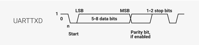
4.2.4. UART hardware flow control
The hardware flow control feature is fully selectable, and enables you to control the serial data flow by using the nUARTRTS output and nUARTCTS input signals. Figure 62 shows how two devices can communicate with each other using hardware flow control.
Figure 62. Hardware flow control between two similar devices.
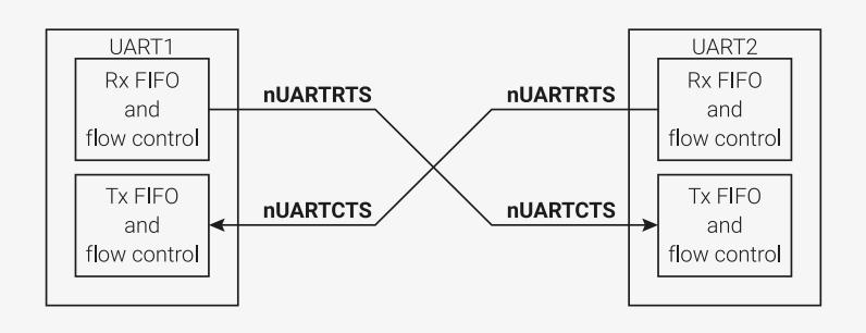
The diagram illustrates the hardware flow control mechanism between two UART devices, UART1 and UART2. Each device contains two main functional blocks: an 'Rx FIFO and flow control' block and a 'Tx FIFO and flow control' block. The flow control is implemented using two signals: nUARTRTS (Request To Send) and nUARTCTS (Clear To Send). The nUARTRTS signal is generated by the Tx FIFO of one device and sent to the Rx FIFO of the other device. Conversely, the nUARTCTS signal is generated by the Rx FIFO of one device and sent to the Tx FIFO of the other device. This setup ensures that data transmission only occurs when the receiving device's FIFO has space available (RTS asserted) and that the transmitter only sends data when it has been granted permission (CTS asserted).
When the RTS flow control is enabled, nUARTRTS is asserted until the receive FIFO is filled up to the programmed watermark level. When the CTS flow control is enabled, the transmitter can only transmit data when nUARTCTS is asserted.
The hardware flow control is selectable using the RTSEn and CTSEn bits in the Control Register, UARTCR . Table 423 lists how you must set the bits to enable RTS and CTS flow control both simultaneously, and independently.
Table 423. Control bits to enable and disable hardware flow control.
| UARTCR Register bits | ||
|---|---|---|
| CTSEn | RTSEn | Description |
| 1 | 1 | Both RTS and CTS flow control enabled |
| 1 | 0 | Only CTS flow control enabled |
| 0 | 1 | Only RTS flow control enabled |
| 0 | 0 | Both RTS and CTS flow control disabled |
NOTE
When RTS flow control is enabled, the software cannot use the RTSEn bit in the Control Register, UARTCR , to control the status of nUARTRTS.
4.2.4.1. RTS flow control
The RTS flow control logic is linked to the programmable receive FIFO watermark levels. When RTS flow control is enabled, the nUARTRTS is asserted until the receive FIFO is filled up to the watermark level. When the receive FIFO watermark level is reached, the nUARTRTS signal is deasserted, indicating that there is no more room to receive any more data. The transmission of data is expected to cease after the current character has been transmitted.
The nUARTRTS signal is reasserted when data has been read out of the receive FIFO so that it is filled to less than the watermark level. If RTS flow control is disabled and the UART is still enabled, then data is received until the receive FIFO is full, or no more data is transmitted to it.
4.2.4.2. CTS flow control
If CTS flow control is enabled, then the transmitter checks the nUARTCTS signal before transmitting the next byte. If the nUARTCTS signal is asserted, it transmits the byte otherwise transmission does not occur.
The data continues to be transmitted while nUARTCTS is asserted, and the transmit FIFO is not empty. If the transmit FIFO is empty and the nUARTCTS signal is asserted no data is transmitted.
If the nUARTCTS signal is deasserted and CTS flow control is enabled, then the current character transmission is completed before stopping. If CTS flow control is disabled and the UART is enabled, then the data continues to be transmitted until the transmit FIFO is empty.
4.2.5. UART DMA Interface
The UART provides an interface to connect to a DMA controller. The DMA operation of the UART is controlled using the DMA Control Register, UARTDMACR . The DMA interface includes the following signals:
For receive:
UARTRXDMASREQ
Single character DMA transfer request, asserted by the UART. For receive, one character consists of up to 12 bits. This signal is asserted when the receive FIFO contains at least one character.
UARTRXDMABREQ
Burst DMA transfer request, asserted by the UART. This signal is asserted when the receive FIFO contains more characters than the programmed watermark level. You can program the watermark level for each FIFO using the Interrupt FIFO Level Select Register, UARTIFLS .
UARTRXDMACLR
DMA request clear, asserted by a DMA controller to clear the receive request signals. If DMA burst transfer is requested, the clear signal is asserted during the transfer of the last data in the burst.
For transmit:
UARTTXDMASREQ
Single character DMA transfer request, asserted by the UART. For transmit one character consists of up to eight bits. This signal is asserted when there is at least one empty location in the transmit FIFO.
UARTTXDMABREQ
Burst DMA transfer request, asserted by the UART. This signal is asserted when the transmit FIFO contains less characters than the watermark level. You can program the watermark level for each FIFO using the Interrupt FIFO Level Select Register, UARTIFLS .
UARTTXDMACLR
DMA request clear, asserted by a DMA controller to clear the transmit request signals. If DMA burst transfer is requested, the clear signal is asserted during the transfer of the last data in the burst.
The burst transfer and single transfer request signals are not mutually exclusive, they can both be asserted at the same time. For example, when there is more data than the watermark level in the receive FIFO, the burst transfer request and the single transfer request are asserted. When the amount of data left in the receive FIFO is less than the watermark level, the single request only is asserted. This is useful for situations where the number of characters left to be received in the stream is less than a burst.
For example, if 19 characters have to be received and the watermark level is programmed to be four. The DMA controller then transfers four bursts of four characters and three single transfers to complete the stream.
 NOTE
NOTE
For the remaining three characters the UART cannot assert the burst request.
Each request signal remains asserted until the relevant DMACLR signal is asserted. After the request clear signal is deasserted, a request signal can become active again, depending on the conditions described previously. All request signals are deasserted if the UART is disabled or the relevant DMA enable bit, TXDMAE or RXDMAE, in the DMA Control Register, UARTDMACR , is cleared.
If you disable the FIFOs in the UART then it operates in character mode and only the DMA single transfer mode can operate, because only one character can be transferred to, or from the FIFOs at any time. UARTRXDMASREQ and UARTTXDMASREQ are the only request signals that can be asserted. See the Line Control Register, UARTLCR_H , for information about disabling the FIFOs.
When the UART is in the FIFO enabled mode, data transfers can be made by either single or burst transfers depending on the programmed watermark level and the amount of data in the FIFO. Table 424 lists the trigger points for UARTRXDMABREQ and UARTTXDMABREQ depending on the watermark level, for the transmit and receive FIFOs.
Table 424. DMA trigger points for the transmit and receive FIFOs.
| Watermark level | Burst length | |
|---|---|---|
| Transmit (number of empty locations) | Receive (number of filled locations) | |
| 1/8 | 28 | 4 |
| 1/4 | 24 | 8 |
| 1/2 | 16 | 16 |
| 3/4 | 8 | 24 |
| 7/8 | 4 | 28 |
In addition, the DMAONERR bit in the DMA Control Register, UARTDMACR , supports the use of the receive error interrupt, UARTEINTR. It enables the DMA receive request outputs, UARTRXDMASREQ or UARTRXDMABREQ, to be masked out when the UART error interrupt, UARTEINTR, is asserted. The DMA receive request outputs remain inactive until the UARTEINTR is cleared. The DMA transmit request outputs are unaffected.
Figure 63. DMA transfer waveforms.

The figure is a timing diagram showing four digital signals over time. The signals are PCLK, DMASREQ, DMABREQ, and DMACLR. PCLK is a periodic square wave. DMASREQ and DMABREQ are pulse signals that occur at specific points in the PCLK cycle. DMACLR is a pulse signal that occurs at the end of each DMA transfer burst.
Figure 63 shows the timing diagram for both a single transfer request and a burst transfer request with the appropriate DMACLR signal. The signals are all synchronous to PCLK. For the sake of clarity it is assumed that there is no synchronization of the request signals in the DMA controller.
4.2.6. Interrupts
There are eleven maskable interrupts generated in the UART. On RP2040, only the combined interrupt output, UARTRINTR , is connected.
You can enable or disable the individual interrupts by changing the mask bits in the Interrupt Mask Set/Clear Register, UARTIMSC . Setting the appropriate mask bit HIGH enables the interrupt.
Provision of individual outputs and the combined interrupt output, enables you to use either a global interrupt service routine, or modular device drivers to handle interrupts.
The transmit and receive dataflow interrupts UARTRXINTR and UARTRXINTR have been separated from the status interrupts. This enables you to use UARTRXINTR and UARTRXINTR so that data can be read or written in response to the FIFO trigger levels.
The error interrupt, UARTEINTR, can be triggered when there is an error in the reception of data. A number of error conditions are possible.
The modem status interrupt, UARTRMSINTR, is a combined interrupt of all the individual modem status signals.
The status of the individual interrupt sources can be read either from the Raw Interrupt Status Register, UARTRIS , or from the Masked Interrupt Status Register, UARTMIS .
4.2.6.1. UARTRMSINTR
The modem status interrupt is asserted if any of the modem status signals (nUARTRCTS, nUARTRDCD, nUARTRDSR, and nUARTRRI) change. It is cleared by writing a 1 to the corresponding bit(s) in the Interrupt Clear Register, UARTICR , depending on the modem status signals that generated the interrupt.
4.2.6.2. UARTRXINTR
The receive interrupt changes state when one of the following events occurs:
- • If the FIFOs are enabled and the receive FIFO reaches the programmed trigger level. When this happens, the receive interrupt is asserted HIGH. The receive interrupt is cleared by reading data from the receive FIFO until it becomes less than the trigger level, or by clearing the interrupt.
- • If the FIFOs are disabled (have a depth of one location) and data is received thereby filling the location, the receive interrupt is asserted HIGH. The receive interrupt is cleared by performing a single read of the receive FIFO, or by clearing the interrupt.
4.2.6.3. UARTRXINTR
The transmit interrupt changes state when one of the following events occurs:
- • If the FIFOs are enabled and the transmit FIFO is equal to or lower than the programmed trigger level then the transmit interrupt is asserted HIGH. The transmit interrupt is cleared by writing data to the transmit FIFO until it becomes greater than the trigger level, or by clearing the interrupt.
- • If the FIFOs are disabled (have a depth of one location) and there is no data present in the transmitters single location, the transmit interrupt is asserted HIGH. It is cleared by performing a single write to the transmit FIFO, or by clearing the interrupt.
To update the transmit FIFO you must:
- • Write data to the transmit FIFO, either prior to enabling the UART and the interrupts, or after enabling the UART and interrupts.
i NOTE
The transmit interrupt is based on a transition through a level, rather than on the level itself. When the interrupt and the UART is enabled before any data is written to the transmit FIFO the interrupt is not set. The interrupt is only set, after written data leaves the single location of the transmit FIFO and it becomes empty.
4.2.6.4. UARTRTINTR
The receive timeout interrupt is asserted when the receive FIFO is not empty, and no more data is received during a 32-bit period. The receive timeout interrupt is cleared either when the FIFO becomes empty through reading all the data (or by reading the holding register), or when a 1 is written to the corresponding bit of the Interrupt Clear Register, UARTICR .
4.2.6.5. UARTEINTR
The error interrupt is asserted when an error occurs in the reception of data by the UART. The interrupt can be caused by a number of different error conditions:
- • framing
- • parity
- • break
- • overrun.
You can determine the cause of the interrupt by reading the Raw Interrupt Status Register, UARTRIS , or the Masked Interrupt Status Register, UARTMIS . It can be cleared by writing to the relevant bits of the Interrupt Clear Register, UARTICR (bits 7 to 10 are the error clear bits).
4.2.6.6. UARTINTR
The interrupts are also combined into a single output, that is an OR function of the individual masked sources. You can connect this output to a system interrupt controller to provide another level of masking on a individual peripheral basis.
The combined UART interrupt is asserted if any of the individual interrupts are asserted and enabled.
4.2.7. Programmer's Model
The SDK provides a
uart_init
function to configure the UART with a particular baud rate. Once the UART is initialised, the user must configure a GPIO pin as
UART_TX
and
UART_RX
. See
Section 2.19.5.1
for more information on selecting a GPIO function.
To initialise the UART, the
uart_init
function takes the following steps:
- • Deassert the reset
- • Enable
clk_peri - • Set enable bits in the control register
- • Enable the FIFOs
- • Set the baud rate divisors
- • Set the format
SDK: https://github.com/raspberrypi/pico-sdk/blob/master/src/tp2_common/hardware_uart/uart.c Lines 42 - 92
42 uint uart_init(uart_inst_t *uart, uint baudrate) {
43     invalid_params_if(HARDWARE_UART, uart != uart0 && uart != uart1);
44
45     if (uart_clock_get_hz(uart) == 0) {
46         return 0;
47     }
48
49     uart_reset(uart);
50     uart_unreset(uart);
51
52     uart_set_translate_crlf(uart, PICO_UART_DEFAULT_CRLF);
53
54     // Any LCR writes need to take place before enabling the UART
55     uint baud = uart_set_baudrate(uart, baudrate);
56
57     // inline the uart_set_format() call, as we don't need the CR disable/re-enable
58     // protection, and also many people will never call it again, so having
59     // the generic function is not useful, and much bigger than this inlined
60     // code which is only a handful of instructions.
61     //
62     // The UART_UARTLCR_H_FEN_BITS setting is combined as well as it is the same register
63 #ifdef 0
64     uart_set_format(uart, 8, 1, UART_PARITY_NONE);
65     // Enable FIFOs (must be before setting UARTEN, as this is an LCR access)
66     hw_set_bits(&uart_get_hw(uart)->lcr_h, UART_UARTLCR_H_FEN_BITS);
67 #else
68     uint data_bits = 8;
69     uint stop_bits = 1;
70     uint parity = UART_PARITY_NONE;
71     hw_write_masked(&uart_get_hw(uart)->lcr_h,
72         ((data_bits - 5u) << UART_UARTLCR_H_WLEN_LSB) |
73         ((stop_bits - 1u) << UART_UARTLCR_H_STP2_LSB) |
74         (bool_to_bit(parity != UART_PARITY_NONE) << UART_UARTLCR_H_PEN_LSB) |
75         (bool_to_bit(parity == UART_PARITY_EVEN) << UART_UARTLCR_H_EPS_LSB) |
76         UART_UARTLCR_H_FEN_BITS,
77         UART_UARTLCR_H_WLEN_BITS | UART_UARTLCR_H_STP2_BITS |
78         UART_UARTLCR_H_PEN_BITS | UART_UARTLCR_H_EPS_BITS |
79         UART_UARTLCR_H_FEN_BITS);
80 #endif
81
82 // Enable the UART, both TX and RX
83 uart_get_hw(uart)->cr = UART_UARTCR_UARTEN_BITS | UART_UARTCR_TXE_BITS |
    UART_UARTCR_RXE_BITS;
84 // Always enable DREQ signals -- no harm in this if DMA is not listening
85 uart_get_hw(uart)->dmacr = UART_UARTDMACR_TXDMAE_BITS | UART_UARTDMACR_RXDMAE_BITS;
86
87 return baud;
88 }
4.2.7.1. Baud Rate Calculation
The uart baud rate is derived from dividing
clk_peri
.
If the required baud rate is 115200 and UARTCLK = 125MHz then:
Baud Rate Divisor = \( (125 * 10^6) / (16 * 115200) \approx 67.817 \)
Therefore, BRDI = 67 and BRDF = 0.817,
Therefore, fractional part, m = integer((0.817 * 64) + 0.5) = 52
Generated baud rate divider = \( 67 + 52/64 = 67.8125 \)
Generated baud rate = \( (125 * 10^6) / (16 * 67.8125) \approx 115207 \)
Error = \( (\text{abs}(115200 - 115207) / 115200) * 100 \approx 0.006\% \)
SDK: https://github.com/raspberrypi/pico-sdk/blob/master/src/rp2-common/hardware_uart/uart.c Lines 155 - 180
155 uint uart_set_baudrate(uart_inst_t *uart, uint baudrate) {
156     invalid_params_if(HARDWARE_UART, baudrate == 0);
157     uint32_t baud_rate_div = (8 * uart_clock_get_hz(uart) / baudrate) + 1;
158     uint32_t baud_ibrd = baud_rate_div >> 7;
159     uint32_t baud_fbrd;
160
161     if (baud_ibrd == 0) {
162         baud_ibrd = 1;
163         baud_fbrd = 0;
164     } else if (baud_ibrd >= 65535) {
165         baud_ibrd = 65535;
166         baud_fbrd = 0;
167     } else {
168         baud_fbrd = (baud_rate_div & 0x7f) >> 1;
169     }
170
171     uart_get_hw(uart)->ibrd = baud_ibrd;
172     uart_get_hw(uart)->fbrd = baud_fbrd;
173
174     // PL011 needs a (dummy) LCR_H write to latch in the divisors.
175     // We don't want to actually change LCR_H contents here.
176     uart_write_lcr_bits_masked(uart, 0, 0);
177
178     // See datasheet
179     return (4 * uart_clock_get_hz(uart)) / (64 * baud_ibrd + baud_fbrd);
180 }
4.2.8. List of Registers
The UART0 and UART1 registers start at base addresses of
0x40034000
and
0x40038000
respectively (defined as
UART0_BASE
and
UART1_BASE
in SDK).
Table 425. List of UART registers
| Offset | Name | Info |
|---|---|---|
| 0x000 | UARTDR | Data Register, UARTDR |
| 0x004 | UARTRSR | Receive Status Register/Error Clear Register, UARTRSR/UARTECR |
| 0x018 | UARTFR | Flag Register, UARTFR |
| 0x020 | UARTILPR | IrDA Low-Power Counter Register, UARTILPR |
| 0x024 | UARTIBRD | Integer Baud Rate Register, UARTIBRD |
| 0x028 | UARTFBRD | Fractional Baud Rate Register, UARTFBRD |
| 0x02c | UARTLCR_H | Line Control Register, UARTLCR_H |
| 0x030 | UARTCR | Control Register, UARTCR |
| 0x034 | UARTIFLS | Interrupt FIFO Level Select Register, UARTIFLS |
| 0x038 | UARTIMSC | Interrupt Mask Set/Clear Register, UARTIMSC |
| 0x03c | UARTRIS | Raw Interrupt Status Register, UARTRIS |
| 0x040 | UARTMIS | Masked Interrupt Status Register, UARTMIS |
| 0x044 | UARTICR | Interrupt Clear Register, UARTICR |
| 0x048 | UARTDMACR | DMA Control Register, UARTDMACR |
| 0xfe0 | UARTPERIPHID0 | UARTPeriphID0 Register |
| 0xfe4 | UARTPERIPHID1 | UARTPeriphID1 Register |
| 0xfe8 | UARTPERIPHID2 | UARTPeriphID2 Register |
| 0xfec | UARTPERIPHID3 | UARTPeriphID3 Register |
| 0xff0 | UARTPCELLID0 | UARTPCellID0 Register |
| 0xff4 | UARTPCELLID1 | UARTPCellID1 Register |
| 0xff8 | UARTPCELLID2 | UARTPCellID2 Register |
| 0xffc | UARTPCELLID3 | UARTPCellID3 Register |
UART: UARTDR Register
Offset: 0x000
Description
Data Register, UARTDR
Table 426. UARTDR Register
| Bits | Description | Type | Reset |
|---|---|---|---|
| 31:12 | Reserved. | - | - |
| 11 | OE: Overrun error. This bit is set to 1 if data is received and the receive FIFO is already full. This is cleared to 0 once there is an empty space in the FIFO and a new character can be written to it. | RO | - |
| Bits | Description | Type | Reset |
|---|---|---|---|
| 10 | BE: Break error. This bit is set to 1 if a break condition was detected, indicating that the received data input was held LOW for longer than a full-word transmission time (defined as start, data, parity and stop bits). In FIFO mode, this error is associated with the character at the top of the FIFO. When a break occurs, only one 0 character is loaded into the FIFO. The next character is only enabled after the receive data input goes to a 1 (marking state), and the next valid start bit is received. | RO | - |
| 9 | PE: Parity error. When set to 1, it indicates that the parity of the received data character does not match the parity that the EPS and SPS bits in the Line Control Register, UARTLCR_H. In FIFO mode, this error is associated with the character at the top of the FIFO. | RO | - |
| 8 | FE: Framing error. When set to 1, it indicates that the received character did not have a valid stop bit (a valid stop bit is 1). In FIFO mode, this error is associated with the character at the top of the FIFO. | RO | - |
| 7:0 | DATA: Receive (read) data character. Transmit (write) data character. | RWF | - |
UART: UARTSR Register
Offset: 0x004
Description
Receive Status Register/Error Clear Register, UARTSR/UARTECR
Table 427. UARTSR Register
| Bits | Description | Type | Reset |
|---|---|---|---|
| 31:4 | Reserved. | - | - |
| 3 | OE: Overrun error. This bit is set to 1 if data is received and the FIFO is already full. This bit is cleared to 0 by a write to UARTECR. The FIFO contents remain valid because no more data is written when the FIFO is full, only the contents of the shift register are overwritten. The CPU must now read the data, to empty the FIFO. | WC | 0x0 |
| 2 | BE: Break error. This bit is set to 1 if a break condition was detected, indicating that the received data input was held LOW for longer than a full-word transmission time (defined as start, data, parity, and stop bits). This bit is cleared to 0 after a write to UARTECR. In FIFO mode, this error is associated with the character at the top of the FIFO. When a break occurs, only one 0 character is loaded into the FIFO. The next character is only enabled after the receive data input goes to a 1 (marking state) and the next valid start bit is received. | WC | 0x0 |
| 1 | PE: Parity error. When set to 1, it indicates that the parity of the received data character does not match the parity that the EPS and SPS bits in the Line Control Register, UARTLCR_H. This bit is cleared to 0 by a write to UARTECR. In FIFO mode, this error is associated with the character at the top of the FIFO. | WC | 0x0 |
| 0 | FE: Framing error. When set to 1, it indicates that the received character did not have a valid stop bit (a valid stop bit is 1). This bit is cleared to 0 by a write to UARTECR. In FIFO mode, this error is associated with the character at the top of the FIFO. | WC | 0x0 |
UART: UARTFR Register
Offset: 0x018
DescriptionFlag Register, UARTFR
Table 428. UARTFR Register
| Bits Register 31:0 Bits | column_2 | Description Description | Type RO Type | Reset 0x00000001 Reset |
|---|---|---|---|---|
| 31:9 | Reserved. | - | - | |
| 8 | RI : Ring indicator. This bit is the complement of the UART ring indicator, | RO | - | |
| 7 | TXFE | : Transmit FIFO empty. The meaning of this bit depends on the state of this bit is set when the transmit holding register is empty. If the FIFO is indicate if there is data in the transmit shift register. | RO | 0x1 |
| 6 | RXFF | : Receive FIFO full. The meaning of this bit depends on the state of the the receive holding register is full. If the FIFO is enabled, the RXFF bit is set when the receive FIFO is full. | RO | 0x0 |
| 5 | TXFF | : Transmit FIFO full. The meaning of this bit depends on the state of the when the transmit FIFO is full. | RO | 0x0 |
| 4 | RXFE | : Receive FIFO empty. The meaning of this bit depends on the state of the when the receive FIFO is empty. | RO | 0x1 |
| 3 | BUSY | : UART busy. If this bit is set to 1, the UART is busy transmitting data. This bit remains set until the complete byte, including all the stop bits, has becomes non-empty, regardless of whether the UART is enabled or not. | RO | 0x0 |
| 2 | DCD | : Data carrier detect. This bit is the complement of the UART data carrier is LOW. | RO | - |
| 1 | DSR | : Data set ready. This bit is the complement of the UART data set ready, | RO | - |
| 0 | CTS | : Clear to send. This bit is the complement of the UART clear to send, : UARTILPR Register | RO | - |
| Bits | : 0x020 Description | Type | Reset | |
| 31:8 | Reserved. | - | - | |
| 7:0 | ILPDVSR : 0x024 | : 8-bit low-power divisor value. These bits are cleared to 0 at reset. : UARTIBRD Register | RW | 0x00 |
UART: UARTILPR Register
Offset: 0x020
DescriptionIrDA Low-Power Counter Register, UARTILPR
Table 429. UARTILPR Register
UART: UARTIBRD Register
Offset: 0x024
Description
Integer Baud Rate Register, UARTIBRD
Table 430. UARTIBRD Register
| Bits Register 31:0 Bits | column_2 | Description Description | Type RO Type | Reset 0x00000001 Reset |
|---|---|---|---|---|
| 31:16 | Reserved. | - | - | |
| 15:0 UART | BAUD_DIVINT | : The integer baud rate divisor. These bits are cleared to 0 on reset. : UARTFBRD Register | RW | 0x0000 |
| Table 431. UARTFBRD Description Bits Register | Description | Type | Reset | |
| 31:6 | Reserved. | - | - | |
| 5:0 UART | BAUD_DIVFRAC | : The fractional baud rate divisor. These bits are cleared to 0 on reset. : UARTLCR_H Register | RW | 0x00 |
| Table 432. Description Bits UARTLCR_H Register | Description | Type | Reset | |
| 31:8 | Reserved. | - | - | |
| 7 | SPS | : Stick parity select. 0 = stick parity is disabled 1 = either: * if the EPS bit is the PEN bit disables parity checking and generation. | RW | 0x0 |
| 6:5 | WLEN bits. | : Word length. These bits indicate the number of data bits transmitted or | RW | 0x0 |
| 4 | FEN | : Enable FIFOs: 0 = FIFOs are disabled (character mode) that is, the FIFOs are enabled (FIFO mode). | RW | 0x0 |
| 3 | STP2 | : Two stop bits select. If this bit is set to 1, two stop bits are transmitted at the end of the frame. The receive logic does not check for two stop bits being received. | RW | 0x0 |
| 2 | EPS | : Even parity select. Controls the type of parity the UART uses during an odd number of 1s in the data and parity bits. 1 = even parity. The UART bit has no effect when the PEN bit disables parity checking and generation. | RW | 0x0 |
| 1 | PEN | : Parity enable: 0 = parity is disabled and no parity bit added to the data frame 1 = parity checking and generation is enabled. | RW | 0x0 |
UART: UARTFBRD Register
Offset: 0x028
Description
Fractional Baud Rate Register, UARTFBRD
Table 431. UARTFBRD Register
UART: UARTLCR_H Register
Offset: 0x02c
Description
Line Control Register, UARTLCR_H
Table 432. UARTLCR_H Register
| Bits Register 31:0 Bits | column_2 | Description Description | Type RO Type | Reset 0x00000001 Reset |
|---|---|---|---|---|
| 31:16 | Reserved. | - | - | |
| 15 | CTSEN | : CTS hardware flow control enable. If this bit is set to 1, CTS hardware asserted. | RW | 0x0 |
| 14 | RTSEN | : RTS hardware flow control enable. If this bit is set to 1, RTS hardware flow control is enabled. Data is only requested when there is space in the receive FIFO for it to be received. | RW | 0x0 |
| 13 | OUT2 | : This bit is the complement of the UART Out2 (nUARTOut2) modem DTE this can be used as Ring Indicator (RI). | RW | 0x0 |
| 12 | OUT1 | : This bit is the complement of the UART Out1 (nUARTOut1) modem DTE this can be used as Data Carrier Detect (DCD). | RW | 0x0 |
| 11 | RTS | : Request to send. This bit is the complement of the UART request to to a 1 then nUARTRTS is LOW. | RW | 0x0 |
| 10 | DTR | : Data transmit ready. This bit is the complement of the UART data transmit ready, nUARTDTR, modem status output. That is, when the bit is programmed to a 1 then nUARTDTR is LOW. | RW | 0x0 |
| 9 | RXE | : Receive enable. If this bit is set to 1, the receive section of the UART is enabled. Data reception occurs for either UART signals or SIR signals middle of reception, it completes the current character before stopping. | RW | 0x1 |
| 8 | TXE | : Transmit enable. If this bit is set to 1, the transmit section of the UART is enabled. Data transmission occurs for either UART signals, or SIR signals | RW | 0x1 |
UART: UARTCR Register
Offset: 0x030
Description
Control Register, UARTCR
Table 433. UARTCR Register
| Bits | Description | Type | Reset |
|---|---|---|---|
| 7 | LBE : Loopback enable. If this bit is set to 1 and the SIREN bit is set to 1 and the SIRTEST bit in the Test Control Register, UAR TTCR is set to 1, then the nSIROUT path is inverted, and fed through to the SIRIN path. The SIRTEST bit in the test register must be set to 1 to override the normal half-duplex SIR operation. This must be the requirement for accessing the test registers during normal operation, and SIRTEST must be cleared to 0 when loopback testing is finished. This feature reduces the amount of external coupling required during system test. If this bit is set to 1, and the SIRTEST bit is set to 0, the UAR TTxD path is fed through to the UAR TRxD path. In either SIR mode or UART mode, when this bit is set, the modem outputs are also fed through to the modem inputs. This bit is cleared to 0 on reset, to disable loopback. | RW | 0x0 |
| 6:3 | Reserved. | - | - |
| 2 | SIRLP : SIR low-power IrDA mode. This bit selects the IrDA encoding mode. If this bit is cleared to 0, low-level bits are transmitted as an active high pulse with a width of 3 / 16th of the bit period. If this bit is set to 1, low-level bits are transmitted with a pulse width that is 3 times the period of the IrLPBaud16 input signal, regardless of the selected bit rate. Setting this bit uses less power, but might reduce transmission distances. | RW | 0x0 |
| 1 | SIREN : SIR enable: 0 = IrDA SIR ENDEC is disabled. nSIROUT remains LOW (no light pulse generated), and signal transitions on SIRIN have no effect. 1 = IrDA SIR ENDEC is enabled. Data is transmitted and received on nSIROUT and SIRIN. UAR TTxD remains HIGH, in the marking state. Signal transitions on UAR TRxD or modem status inputs have no effect. This bit has no effect if the UAR TEN bit disables the UART. | RW | 0x0 |
| 0 | UAR TEN : UART enable: 0 = UART is disabled. If the UART is disabled in the middle of transmission or reception, it completes the current character before stopping. 1 = the UART is enabled. Data transmission and reception occurs for either UART signals or SIR signals depending on the setting of the SIREN bit. | RW | 0x0 |
UART: UARTIFLS Register
Offset: 0x034
Description
Interrupt FIFO Level Select Register, UARTIFLS
Table 434. UARTIFLS Register
| Bits | Description | Type | Reset |
|---|---|---|---|
| 31:6 | Reserved. | - | - |
| 5:3 | RXIFLSEL : Receive interrupt FIFO level select. The trigger points for the receive interrupt are as follows: b000 = Receive FIFO becomes \( \geq 1 / 8 \) full b001 = Receive FIFO becomes \( \geq 1 / 4 \) full b010 = Receive FIFO becomes \( \geq 1 / 2 \) full b011 = Receive FIFO becomes \( \geq 3 / 4 \) full b100 = Receive FIFO becomes \( \geq 7 / 8 \) full b101-b111 = reserved. | RW | 0x2 |
| 2:0 | TXIFLSEL : Transmit interrupt FIFO level select. The trigger points for the transmit interrupt are as follows: b000 = Transmit FIFO becomes \( \leq 1 / 8 \) full b001 = Transmit FIFO becomes \( \leq 1 / 4 \) full b010 = Transmit FIFO becomes \( \leq 1 / 2 \) full b011 = Transmit FIFO becomes \( \leq 3 / 4 \) full b100 = Transmit FIFO becomes \( \leq 7 / 8 \) full b101-b111 = reserved. | RW | 0x2 |
UART: UARTIMSC Register
Offset: 0x038 DescriptionInterrupt Mask Set/Clear Register, UARTIMSC
Table 435. UARTIMSC Register
| Bits Register 31:0 Bits | column_2 | Description Description | Type RO Type | Reset 0x00000001 Reset |
|---|---|---|---|---|
| 31:11 | Reserved. | - | - | |
| 10 | OEIM | : Overrun error interrupt mask. A read returns the current mask for the is set. A write of 0 clears the mask. | RW | 0x0 |
| 9 | BEIM | : Break error interrupt mask. A read returns the current mask for the is set. A write of 0 clears the mask. | RW | 0x0 |
| 8 | PEIM | : Parity error interrupt mask. A read returns the current mask for the is set. A write of 0 clears the mask. | RW | 0x0 |
| 7 | FEIM | : Framing error interrupt mask. A read returns the current mask for the is set. A write of 0 clears the mask. | RW | 0x0 |
| 6 | RTIM | : Receive timeout interrupt mask. A read returns the current mask for the is set. A write of 0 clears the mask. | RW | 0x0 |
| 5 | TXIM | : Transmit interrupt mask. A read returns the current mask for the is set. A write of 0 clears the mask. | RW | 0x0 |
| 4 | RXIM | : Receive interrupt mask. A read returns the current mask for the is set. A write of 0 clears the mask. | RW | 0x0 |
| 3 | DSRMIM | : nUARTDSR modem interrupt mask. A read returns the current mask for the UARTDSRINTR interrupt. On a write of 1, the mask of the UARTDSRINTR interrupt is set. A write of 0 clears the mask. | RW | 0x0 |
| 2 | DCDMIM | : nUARTDCD modem interrupt mask. A read returns the current mask for the UARTDCDINTR interrupt. On a write of 1, the mask of the UARTDCDINTR interrupt is set. A write of 0 clears the mask. | RW | 0x0 |
| 1 | CTSMIM | : nUARTCTS modem interrupt mask. A read returns the current mask for the UARTCTSINTR interrupt. On a write of 1, the mask of the UARTCTSINTR interrupt is set. A write of 0 clears the mask. | RW | 0x0 |
| 0 | RIMIM | : nUARTRI modem interrupt mask. A read returns the current mask for the UARTRIINTR interrupt. On a write of 1, the mask of the UARTRIINTR interrupt is set. A write of 0 clears the mask. : UARTRIS Register | RW | 0x0 |
| Bits | Description | Type | Reset | |
| 31:11 | Reserved. | - | - |
Raw Interrupt Status Register, UARTRIS
Table 436. UARTRIS Register
| Bits | Description | Type | Reset |
|---|---|---|---|
| 10 | OERIS : Overrun error interrupt status. Returns the raw interrupt state of the UARTOEINTR interrupt. | RO | 0x0 |
| 9 | BERIS : Break error interrupt status. Returns the raw interrupt state of the UARTBEINTR interrupt. | RO | 0x0 |
| 8 | PERIS : Parity error interrupt status. Returns the raw interrupt state of the UARTPEINTR interrupt. | RO | 0x0 |
| 7 | FERIS : Framing error interrupt status. Returns the raw interrupt state of the UARTFEINTR interrupt. | RO | 0x0 |
| 6 | RTRIS : Receive timeout interrupt status. Returns the raw interrupt state of the UARTRTINTR interrupt. a | RO | 0x0 |
| 5 | TXRIS : Transmit interrupt status. Returns the raw interrupt state of the UARTTXINTR interrupt. | RO | 0x0 |
| 4 | RXRIS : Receive interrupt status. Returns the raw interrupt state of the UARTRXINTR interrupt. | RO | 0x0 |
| 3 | DSRRMIS : nUARTDSR modem interrupt status. Returns the raw interrupt state of the UARTDSRINTR interrupt. | RO | - |
| 2 | DCDRMIS : nUARTDCD modem interrupt status. Returns the raw interrupt state of the UARTDCDINTR interrupt. | RO | - |
| 1 | CTSRMIS : nUARTCTS modem interrupt status. Returns the raw interrupt state of the UARTCTSINTR interrupt. | RO | - |
| 0 | RIRMIS : nUARTRI modem interrupt status. Returns the raw interrupt state of the UARTRIINTR interrupt. | RO | - |
UART: UARTMIS Register
Offset: 0x040
Description
Masked Interrupt Status Register, UARTMIS
Table 437. UARTMIS Register
| Bits | Description | Type | Reset |
|---|---|---|---|
| 31:11 | Reserved. | - | - |
| 10 | OEMIS : Overrun error masked interrupt status. Returns the masked interrupt state of the UARTOEINTR interrupt. | RO | 0x0 |
| 9 | BEMIS : Break error masked interrupt status. Returns the masked interrupt state of the UARTBEINTR interrupt. | RO | 0x0 |
| 8 | PEMIS : Parity error masked interrupt status. Returns the masked interrupt state of the UARTPEINTR interrupt. | RO | 0x0 |
| 7 | FEMIS : Framing error masked interrupt status. Returns the masked interrupt state of the UARTFEINTR interrupt. | RO | 0x0 |
| 6 | RTMIS : Receive timeout masked interrupt status. Returns the masked interrupt state of the UARTRTINTR interrupt. | RO | 0x0 |
| 5 | TXMIS : Transmit masked interrupt status. Returns the masked interrupt state of the UARTTXINTR interrupt. | RO | 0x0 |
| Bits | Description | Type | Reset |
|---|---|---|---|
| 4 | RXMIS : Receive masked interrupt status. Returns the masked interrupt state of the UARTRXINTR interrupt. | RO | 0x0 |
| 3 | DSRMMIS : nUARTDSR modem masked interrupt status. Returns the masked interrupt state of the UARTDSRINTR interrupt. | RO | - |
| 2 | DCDMMIS : nUARTDCD modem masked interrupt status. Returns the masked interrupt state of the UARTDCDINTR interrupt. | RO | - |
| 1 | CTSMMIS : nUARTCTS modem masked interrupt status. Returns the masked interrupt state of the UARTCTSINTR interrupt. | RO | - |
| 0 | RIMMIS : nUARTRI modem masked interrupt status. Returns the masked interrupt state of the UARTRIINTR interrupt. | RO | - |
UART: UARTICR Register
Offset: 0x044
Description
Interrupt Clear Register, UARTICR
Table 438. UARTICR Register
| Bits | Description | Type | Reset |
|---|---|---|---|
| 31:11 | Reserved. | - | - |
| 10 | OEIC : Overrun error interrupt clear. Clears the UARTOEINTR interrupt. | WC | - |
| 9 | BEIC : Break error interrupt clear. Clears the UARTBEINTR interrupt. | WC | - |
| 8 | PEIC : Parity error interrupt clear. Clears the UARTPEINTR interrupt. | WC | - |
| 7 | FEIC : Framing error interrupt clear. Clears the UARTFEINTR interrupt. | WC | - |
| 6 | RTIC : Receive timeout interrupt clear. Clears the UARTRTINTR interrupt. | WC | - |
| 5 | TXIC : Transmit interrupt clear. Clears the UARTTXINTR interrupt. | WC | - |
| 4 | RXIC : Receive interrupt clear. Clears the UARTRXINTR interrupt. | WC | - |
| 3 | DSRMIC : nUARTDSR modem interrupt clear. Clears the UARTDSRINTR interrupt. | WC | - |
| 2 | DCDMIC : nUARTDCD modem interrupt clear. Clears the UARTDCDINTR interrupt. | WC | - |
| 1 | CTSMIC : nUARTCTS modem interrupt clear. Clears the UARTCTSINTR interrupt. | WC | - |
| 0 | RIMIC : nUARTRI modem interrupt clear. Clears the UARTRIINTR interrupt. | WC | - |
UART: UARTDMACR Register
Offset: 0x048
Description
DMA Control Register, UARTDMACR
Table 439. UARTDMACR Register
| Bits | Description | Type | Reset |
|---|---|---|---|
| 31:3 | Reserved. | - | - |
| Bits | Description | Type | Reset |
|---|---|---|---|
| 2 | DMAONERR : DMA on error. If this bit is set to 1, the DMA receive request outputs, UARTRXDMASREQ or UARTRXDMAREQ, are disabled when the UART error interrupt is asserted. | RW | 0x0 |
| 1 | TXDMAE : Transmit DMA enable. If this bit is set to 1, DMA for the transmit FIFO is enabled. | RW | 0x0 |
| 0 | RXDMAE : Receive DMA enable. If this bit is set to 1, DMA for the receive FIFO is enabled. | RW | 0x0 |
UART: UARTPERIPHID0 Register
Offset: 0xfe0
Description
UARTPeriphID0 Register
Table 440.
UARTPERIPHID0
Register
| Bits | Description | Type | Reset |
|---|---|---|---|
| 31:8 | Reserved. | - | - |
| 7:0 | PARTNUMBER0 : These bits read back as 0x11 | RO | 0x11 |
UART: UARTPERIPHID1 Register
Offset: 0xfe4
Description
UARTPeriphID1 Register
Table 441.
UARTPERIPHID1
Register
| Bits | Description | Type | Reset |
|---|---|---|---|
| 31:8 | Reserved. | - | - |
| 7:4 | DESIGNER0 : These bits read back as 0x1 | RO | 0x1 |
| 3:0 | PARTNUMBER1 : These bits read back as 0x0 | RO | 0x0 |
UART: UARTPERIPHID2 Register
Offset: 0xfe8
Description
UARTPeriphID2 Register
Table 442.
UARTPERIPHID2
Register
| Bits | Description | Type | Reset |
|---|---|---|---|
| 31:8 | Reserved. | - | - |
| 7:4 | REVISION : This field depends on the revision of the UART: r1p0 0x0 r1p1 0x1 r1p3 0x2 r1p4 0x2 r1p5 0x3 | RO | 0x3 |
| 3:0 | DESIGNER1 : These bits read back as 0x4 | RO | 0x4 |
UART: UARTPERIPHID3 Register
Offset: 0xfec
Description
UARTPeriphID3 Register
Table 443.
UARTPERIPHD3
Register
| Bits | Description | Type | Reset |
|---|---|---|---|
| 31:8 | Reserved. | - | - |
| 7:0 | CONFIGURATION : These bits read back as 0x00 | RO | 0x00 |
UART: UARTPCELLID0 Register
Offset: 0xff0
Description
UARTPCellID0 Register
Table 444.
UARTPCELLID0
Register
| Bits | Description | Type | Reset |
|---|---|---|---|
| 31:8 | Reserved. | - | - |
| 7:0 | UARTPCELLID0 : These bits read back as 0x0D | RO | 0x0d |
UART: UARTPCELLID1 Register
Offset: 0xff4
Description
UARTPCellID1 Register
Table 445.
UARTPCELLID1
Register
| Bits | Description | Type | Reset |
|---|---|---|---|
| 31:8 | Reserved. | - | - |
| 7:0 | UARTPCELLID1 : These bits read back as 0xF0 | RO | 0xf0 |
UART: UARTPCELLID2 Register
Offset: 0xff8
Description
UARTPCellID2 Register
Table 446.
UARTPCELLID2
Register
| Bits | Description | Type | Reset |
|---|---|---|---|
| 31:8 | Reserved. | - | - |
| 7:0 | UARTPCELLID2 : These bits read back as 0x05 | RO | 0x05 |
UART: UARTPCELLID3 Register
Offset: 0xffc
Description
UARTPCellID3 Register
Table 447.
UARTPCELLID3
Register
| Bits | Description | Type | Reset |
|---|---|---|---|
| 31:8 | Reserved. | - | - |
| 7:0 | UARTPCELLID3 : These bits read back as 0xB1 | RO | 0xb1 |
4.3. I2C
Synopsys Documentation
Synopsys Proprietary. Used with permission.
I2C is a commonly used 2-wire interface that can be used to connect devices for low speed data transfer using clock SCL and data SDA wires.
RP2040 has two identical instances of an I2C controller. The external pins of each controller are connected to GPIO pins as defined in the GPIO muxing table in Section 2.19.2 . The muxing options give some IO flexibility.
4.3.1. Features
Each I2C controller is based on a configuration of the Synopsys DW_apb_i2c (v2.01) IP. The following features are supported:
- • Master or Slave (Default to Master mode)
- • Standard mode, Fast mode or Fast mode plus
- • Default slave address 0x055
- • Supports 10-bit addressing in Master mode
- • 16-element transmit buffer
- • 16-element receive buffer
- • Can be driven from DMA
- • Can generate interrupts
4.3.1.1. Standard
The I2C controller was designed for I2C Bus specification, version 6.0, dated April 2014.
4.3.1.2. Clocking
All clocks in the I2C controller are connected to clk_sys , including ic_clk which is mentioned in later sections. The I2C clock is generated by dividing down this clock, controlled by registers inside the block.
4.3.1.3. IOs
Each controller must connect its clock SCL and data SDA to one pair of GPIOs. The I2C standard requires that drivers drive a signal low, or when not driven the signal will be pulled high. This applies to SCL and SDA. The GPIO pads should be configured for:
- • pull-up enabled
- • slew rate limited
- • schmitt trigger enabled
There should also be external pull-ups on the board as the internal pad pull-ups may not be strong enough to pull up external circuits.
4.3.2. IP Configuration
I2C configuration details (each instance is fully independent):
- • 32-bit APB access
- • Supports Standard mode, Fast mode or Fast mode plus (not High speed)
- • Default slave address of 0x055
- • Master or Slave mode
- • Master by default (Slave mode disabled at reset)
- • 10-bit addressing supported in master mode (7-bit by default)
- • 16 entry transmit buffer
- • 16 entry receive buffer
- • Allows restart conditions when a master (can be disabled for legacy device support)
- • Configurable timing to adjust TsuDAT/ThDAT
- • General calls responded to on reset
- • Interface to DMA
- • Single interrupt output
- • Configurable timing to adjust clock frequency
- • Spike suppression (default 7 clk_sys cycles)
- • Can NACK after data received by Slave
- • Hold transfer when TX FIFO empty
- • Hold bus until space available in RX FIFO
- • Restart detect interrupt in Slave mode
- • Optional blocking Master commands (not enabled by default)
4.3.3. I2C Overview
The I2C bus is a 2-wire serial interface, consisting of a serial data line SDA and a serial clock SCL . These wires carry information between the devices connected to the bus. Each device is recognized by a unique address and can operate as either a “transmitter” or “receiver”, depending on the function of the device. Devices can also be considered as masters or slaves when performing data transfers. A master is a device that initiates a data transfer on the bus and generates the clock signals to permit that transfer. At that time, any device addressed is considered a slave.
NOTE
The I2C block must only be programmed to operate in either master OR slave mode only. Operating as a master and slave simultaneously is not supported.
The I2C block can operate in these modes:
- • standard mode (with data rates from 0 to 100kbps),
- • fast mode (with data rates less than or equal to 400kbps),
- • fast mode plus (with data rates less than or equal to 1000kbps).
These modes are not supported:
- • High-speed mode (with data rates less than or equal to 3.4Mbps),
- • Ultra-Fast Speed Mode (with data rates less than or equal to 5Mbps).
NOTE
References to fast mode also apply to fast mode plus, unless specifically stated otherwise.
The I2C block can communicate with devices in one of these modes as long as they are attached to the bus. Additionally, fast mode devices are downward compatible. For instance, fast mode devices can communicate with standard mode devices in 0 to 100kbps I2C bus system. However standard mode devices are not upward compatible and should not be incorporated in a fast-mode I2C bus system as they cannot follow the higher transfer rate and unpredictable states would occur.
An example of high-speed mode devices are LCD displays, high-bit count ADCs, and high capacity EEPROMs. These devices typically need to transfer large amounts of data. Most maintenance and control applications, the common use for the I2C bus, typically operate at 100kHz (in standard and fast modes). Any DW_apb_i2c device can be attached to an I2C-bus and every device can talk with any master, passing information back and forth. There needs to be at least one master (such as a microcontroller or DSP) on the bus but there can be multiple masters, which require them to arbitrate for ownership. Multiple masters and arbitration are explained later in this chapter. The I2C block does not support SMBus and PMBus protocols (for System Management and Power management).
The DW_apb_i2c is made up of an AMBA APB slave interface, an I2C interface, and FIFO logic to maintain coherency between the two interfaces. The blocks of the component are illustrated in Figure 64 .
Figure 64. I2C Block diagram
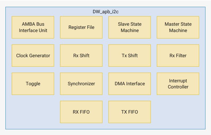
graph TD
    subgraph DW_apb_i2c
        direction TB
        subgraph Row1
            A[AMBA Bus Interface Unit]
            B[Register File]
            C[Slave State Machine]
            D[Master State Machine]
        end
        subgraph Row2
            E[Clock Generator]
            F[Rx Shift]
            G[Tx Shift]
            H[Rx Filter]
        end
        subgraph Row3
            I[Toggle]
            J[Synchronizer]
            K[DMA Interface]
            L[Interrupt Controller]
        end
        subgraph Row4
            M[RX FIFO]
            N[TX FIFO]
        end
endThe following define the functions of the blocks in Figure 64 :
- • AMBA Bus Interface Unit — Takes the APB interface signals and translates them into a common generic interface that allows the register file to be bus protocol-agnostic.
- • Register File — Contains configuration registers and is the interface with software.
- • Slave State Machine — Follows the protocol for a slave and monitors bus for address match.
- • Master State Machine — Generates the I2C protocol for the master transfers.
- •
Clock Generator
— Calculates the required timing to do the following:
- ◦ Generate the SCL clock when configured as a master
- ◦ Check for bus idle
- ◦ Generate a START and a STOP
- ◦ Setup the data and hold the data
- • Rx Shift — Takes data into the design and extracts it in byte format.
- • Tx Shift — Presents data supplied by CPU for transfer on the I2C bus.
- • Rx Filter — Detects the events in the bus; for example, start, stop and arbitration lost.
- • Toggle — Generates pulses on both sides and toggles to transfer signals across clock domains.
- • Synchronizer — Transfers signals from one clock domain to another.
- • DMA Interface — Generates the handshaking signals to the central DMA controller in order to automate the data transfer without CPU intervention.
- • Interrupt Controller — Generates the raw interrupt and interrupt flags, allowing them to be set and cleared.
- • RX FIFO/TX FIFO — Holds the RX FIFO and TX FIFO register banks and controllers, along with their status levels.
4.3.4. I2C Terminology
The following terms are used and are defined as follows:
4.3.4.1. I2C Bus Terms
The following terms relate to how the role of the I2C device and how it interacts with other I2C devices on the bus.
- • Transmitter — the device that sends data to the bus. A transmitter can either be a device that initiates the data transmission to the bus (a master-transmitter) or responds to a request from the master to send data to the bus (a slave-transmitter).
- • Receiver — the device that receives data from the bus. A receiver can either be a device that receives data on its own request (a master-receiver) or in response to a request from the master (a slave-receiver).
- • Master — the component that initializes a transfer (START command), generates the clock SCL signal and terminates the transfer (STOP command). A master can be either a transmitter or a receiver.
- • Slave — the device addressed by the master. A slave can be either receiver or transmitter.
- • Multi-master — the ability for more than one master to co-exist on the bus at the same time without collision or data loss.
- • Arbitration — the predefined procedure that authorizes only one master at a time to take control of the bus. For more information about this behaviour, refer to Section 4.3.8 .
- • Synchronization — the predefined procedure that synchronizes the clock signals provided by two or more masters. For more information about this feature, refer to Section 4.3.9 .
- • SDA — data signal line (Serial Data)
- • SCL — clock signal line (Serial Clock)
4.3.4.2. Bus Transfer Terms
The following terms are specific to data transfers that occur to/from the I2C bus.
- • START (RESTART) – data transfer begins with a START or RESTART condition. The level of the SDA data line changes from high to low, while the SCL clock line remains high. When this occurs, the bus becomes busy.
NOTE
START and RESTART conditions are functionally identical.
- • STOP – data transfer is terminated by a STOP condition. This occurs when the level on the SDA data line passes from the low state to the high state, while the SCL clock line remains high. When the data transfer has been terminated, the bus is free or idle once again. The bus stays busy if a RESTART is generated instead of a STOP condition.
4.3.5. I2C Behaviour
The DW_apb_i2c can be controlled via software to be either:
- • An I2C master only, communicating with other I2C slaves; OR
- • An I2C slave only, communicating with one or more I2C masters.
The master is responsible for generating the clock and controlling the transfer of data. The slave is responsible for either transmitting or receiving data to/from the master. The acknowledgement of data is sent by the device that is receiving data, which can be either a master or a slave. As mentioned previously, the I2C protocol also allows multiple masters to reside on the I2C bus and uses an arbitration procedure to determine bus ownership.
Each slave has a unique address that is determined by the system designer. When a master wants to communicate with a slave, the master transmits a START/RESTART condition that is then followed by the slave’s address and a control bit (R/W) to determine if the master wants to transmit data or receive data from the slave. The slave then sends an acknowledge (ACK) pulse after the address.
If the master (master-transmitter) is writing to the slave (slave-receiver), the receiver gets one byte of data. This transaction continues until the master terminates the transmission with a STOP condition. If the master is reading from a slave (master-receiver), the slave transmits (slave-transmitter) a byte of data to the master, and the master then acknowledges the transaction with the ACK pulse. This transaction continues until the master terminates the transmission by not acknowledging (NACK) the transaction after the last byte is received, and then the master issues a STOP condition or addresses another slave after issuing a RESTART condition. This behaviour is illustrated in Figure 65.
Figure 65. Data transfer on the I2C Bus
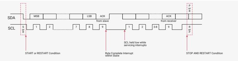
The diagram shows the SDA and SCL signals over time. The SDA line has a START or RESTART condition (low-to-high transition while SCL is high), followed by data transmission (MSB to LSB), an ACK from the slave (low-to-high transition while SCL is high), a period where SCL is held low while servicing interrupts, data reception (1 to 3-8), an ACK from the receiver (low-to-high transition while SCL is high), and finally a STOP AND RESTART condition (high-to-low transition while SCL is high). The SCL line shows clock pulses and a low state during interrupts.
The DW_apb_i2c is a synchronous serial interface. The SDA line is a bidirectional signal and changes only while the SCL line is low, except for STOP, START, and RESTART conditions. The output drivers are open-drain or open-collector to perform wire-AND functions on the bus. The maximum number of devices on the bus is limited by only the maximum capacitance specification of 400 pF. Data is transmitted in byte packages.
The I2C protocols implemented in DW_apb_i2c are described in more details in Section 4.3.6.
4.3.5.1. START and STOP Generation
When operating as an I2C master, putting data into the transmit FIFO causes the DW_apb_i2c to generate a START condition on the I2C bus. Writing a 1 to IC_DATA_CMD.STOP causes the DW_apb_i2c to generate a STOP condition on
the I2C bus; a STOP condition is not issued if this bit is not set, even if the transmit FIFO is empty.
When operating as a slave, the DW_apb_i2c does not generate START and STOP conditions, as per the protocol. However, if a read request is made to the DW_apb_i2c, it holds the SCL line low until read data has been supplied to it. This stalls the I2C bus until read data is provided to the slave DW_apb_i2c, or the DW_apb_i2c slave is disabled by writing a 0 to IC_ENABLE.ENABLE .
4.3.5.2. Combined Formats
The DW_apb_i2c supports mixed read and write combined format transactions in both 7-bit and 10-bit addressing modes. The DW_apb_i2c does not support mixed address and mixed address format—that is, a 7-bit address transaction followed by a 10-bit address transaction or vice versa—combined format transactions. To initiate combined format transfers, IC_CON.IC_RESTART_EN should be set to 1. With this value set and operating as a master, when the DW_apb_i2c completes an I2C transfer, it checks the transmit FIFO and executes the next transfer. If the direction of this transfer differs from the previous transfer, the combined format is used to issue the transfer. If the transmit FIFO is empty when the current I2C transfer completes:
- •
IC_DATA_CMD.STOP
is checked and:
- ◦ If set to 1, a STOP bit is issued.
- ◦ If set to 0, the SCL is held low until the next command is written to the transmit FIFO.
For more details, refer to Section 4.3.7 .
4.3.6. I2C Protocols
The DW_apb_i2c has the protocols discussed in this section.
4.3.6.1. START and STOP Conditions
When the bus is idle, both the SCL and SDA signals are pulled high through external pull-up resistors on the bus. When the master wants to start a transmission on the bus, the master issues a START condition. This is defined to be a high-to-low transition of the SDA signal while SCL is 1. When the master wants to terminate the transmission, the master issues a STOP condition. This is defined to be a low-to-high transition of the SDA line while SCL is 1. Figure 66 shows the timing of the START and STOP conditions. When data is being transmitted on the bus, the SDA line must be stable when SCL is 1.
Figure 66. I2C START and STOP Condition
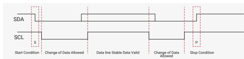
i NOTE
The signal transitions for the START/STOP conditions, as depicted in Figure 66 , reflect those observed at the output signals of the Master driving the I2C bus. Care should be taken when observing the SDA/SCL signals at the input signals of the Slave(s), because unequal line delays may result in an incorrect SDA/SCL timing relationship.
4.3.6.2. Addressing Slave Protocol
There are two address formats: the 7-bit address format and the 10-bit address format.
4.3.6.2.1. 7-bit Address Format
During the 7-bit address format, the first seven bits (bits 7:1) of the first byte set the slave address and the LSB bit (bit 0) is the R/W bit as shown in Figure 67 . When bit 0 (R/W) is set to 0, the master writes to the slave. When bit 0 (R/W) is set to 1, the master reads from the slave.
Figure 67. I2C 7-bit Address Format
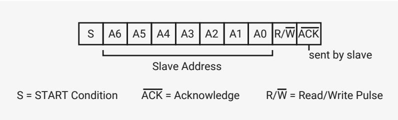
S A6 A5 A4 A3 A2 A1 A0 R/W \( \overline{\text{ACK}} \)
Slave Address
sent by slave
S = START Condition \( \overline{\text{ACK}} \) = Acknowledge R/W = Read/Write Pulse
4.3.6.2.2. 10-bit Address Format
During 10-bit addressing, two bytes are transferred to set the 10-bit address. The transfer of the first byte contains the following bit definition. The first five bits (bits 7:3) notify the slaves that this is a 10-bit transfer followed by the next two bits (bits 2:1), which set the slaves address bits 9:8, and the LSB bit (bit 0) is the R/W bit. The second byte transferred sets bits 7:0 of the slave address. Figure 68 shows the 10-bit address format.
Figure 68. 10-bit Address Format
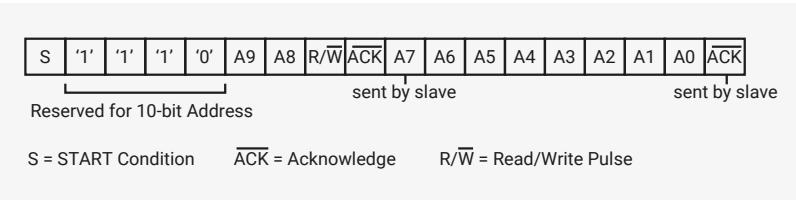
S '1' '1' '1' '0' A9 A8 R/W \( \overline{\text{ACK}} \) A7 A6 A5 A4 A3 A2 A1 A0 \( \overline{\text{ACK}} \)
Reserved for 10-bit Address
sent by slave
sent by slave
S = START Condition \( \overline{\text{ACK}} \) = Acknowledge R/W = Read/Write Pulse
This table defines the special purpose and reserved first byte addresses.
Table 448. I2C/SMBus Definition of Bits in First Byte
| Slave Address | R/W Bit | Description |
|---|---|---|
| 0000 000 | 0 | General Call Address. DW_apb_i2c places the data in the receive buffer and issues a General Call interrupt. |
| 0000 000 | 1 | START byte. For more details, refer to Section 4.3.6.4 . |
| 0000 001 | X | CBUS address. DW_apb_i2c ignores these accesses. |
| 0000 010 | X | Reserved. |
| 0000 011 | X | Reserved. |
| 0000 1XX | X | High-speed master code (for more information, refer to Section 4.3.8 ). |
| 1111 1XX | X | Reserved. |
| 1111 0XX | X | 10-bit slave addressing. |
| 0001 000 | X | SMBus Host (not supported) |
| 0001 100 | X | SMBus Alert Response Address (not supported) |
| 1100 001 | X | SMBus Device Default Address (not supported) |
DW_apb_i2c does not restrict you from using these reserved addresses. However, if you use these reserved addresses,
you may run into incompatibilities with other I2C components.
4.3.6.3. Transmitting and Receiving Protocol
The master can initiate data transmission and reception to/from the bus, acting as either a master-transmitter or master-receiver. A slave responds to requests from the master to either transmit data or receive data to/from the bus, acting as either a slave-transmitter or slave-receiver, respectively.
4.3.6.3.1. Master-Transmitter and Slave-Receiver
All data is transmitted in byte format, with no limit on the number of bytes transferred per data transfer. After the master sends the address and R/W bit or the master transmits a byte of data to the slave, the slave-receiver must respond with the acknowledge signal (ACK). When a slave-receiver does not respond with an ACK pulse, the master aborts the transfer by issuing a STOP condition. The slave must leave the SDA line high so that the master can abort the transfer. If the master-transmitter is transmitting data as shown in Figure 69 , then the slave-receiver responds to the master-transmitter with an acknowledge pulse after every byte of data is received.
Figure 69. I2C Master-Transmitter Protocol
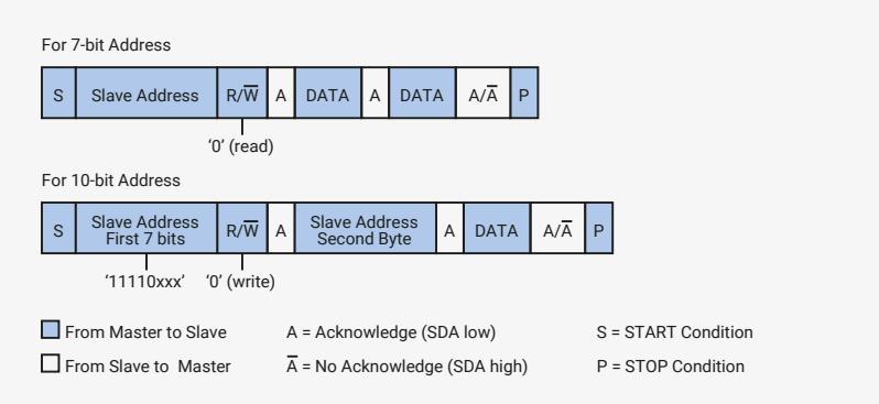
The diagram illustrates the I2C Master-Transmitter Protocol for two address formats:
- For 7-bit Address: The sequence starts with a START condition (S), followed by the Slave Address (7 bits), the Read/Write bit (R/W), an Acknowledge (A), and then two DATA bytes. Each DATA byte is followed by an Acknowledge (A) from the slave. The sequence ends with a No Acknowledge (A-bar) and a STOP condition (P).
- For 10-bit Address: The sequence starts with a START condition (S), followed by the Slave Address First 7 bits, the Read/Write bit (R/W), an Acknowledge (A), the Slave Address Second Byte, and then a DATA byte. Each DATA byte is followed by an Acknowledge (A) from the slave. The sequence ends with a No Acknowledge (A-bar) and a STOP condition (P).
Legend:
- Blue box: From Master to Slave
- White box: From Slave to Master
- A = Acknowledge (SDA low)
- A-bar = No Acknowledge (SDA high)
- S = START Condition
- P = STOP Condition
4.3.6.3.2. Master-Receiver and Slave-Transmitter
If the master is receiving data as shown in Figure 70 , then the master responds to the slave-transmitter with an acknowledge pulse after a byte of data has been received, except for the last byte. This is the way the master-receiver notifies the slave-transmitter that this is the last byte. The slave-transmitter relinquishes the SDA line after detecting the No Acknowledge (NACK) so that the master can issue a STOP condition.
Figure 70. I2C Master-Receiver Protocol
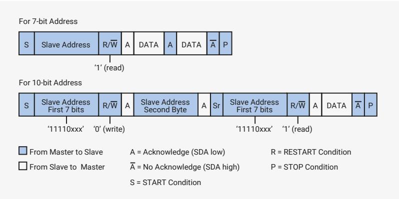
The diagram illustrates the I2C Master-Receiver Protocol for two address formats:
- For 7-bit Address: The sequence starts with a START condition (S), followed by the Slave Address (7 bits), the Read/Write bit (R/W), an Acknowledge (A), and then two DATA bytes. Each DATA byte is followed by an Acknowledge (A) from the master. The sequence ends with a No Acknowledge (A-bar) and a STOP condition (P).
- For 10-bit Address: The sequence starts with a START condition (S), followed by the Slave Address First 7 bits, the Read/Write bit (R/W), an Acknowledge (A), the Slave Address Second Byte, and then a DATA byte. Each DATA byte is followed by an Acknowledge (A) from the master. The sequence ends with a No Acknowledge (A-bar) and a STOP condition (P).
Legend:
- Blue box: From Master to Slave
- White box: From Slave to Master
- A = Acknowledge (SDA low)
- A-bar = No Acknowledge (SDA high)
- S = START Condition
- R = RESTART Condition
- P = STOP Condition
When a master does not want to relinquish the bus with a STOP condition, the master can issue a RESTART condition. This is identical to a START condition except it occurs after the ACK pulse. Operating in master mode, the DW_apb_i2c can then communicate with the same slave using a transfer of a different direction. For a description of the combined format transactions that the DW_apb_i2c supports, refer to Section 4.3.5.2 .
NOTEThe DW_apb_i2c must be completely disabled before the target slave address register ( IC_TAR ) can be reprogrammed.
4.3.6.4. START BYTE Transfer ProtocolThe START BYTE transfer protocol is set up for systems that do not have an on-board dedicated I2C hardware module. When the DW_apb_i2c is addressed as a slave, it always samples the I2C bus at the highest speed supported so that it never requires a START BYTE transfer. However, when DW_apb_i2c is a master, it supports the generation of START BYTE transfers at the beginning of every transfer in case a slave device requires it.
This protocol consists of seven zeros being transmitted followed by a one, as illustrated in Figure 71 . This allows the processor that is polling the bus to under-sample the address phase until zero is detected. Once the microcontroller detects a zero, it switches from the under sampling rate to the correct rate of the master.
Figure 71. I2C Start Byte Transfer
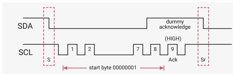
The START BYTE procedure is as follows:
- 1. Master generates a START condition.
- 2. Master transmits the START byte (0000 0001).
- 3. Master transmits the ACK clock pulse. (Present only to conform with the byte handling format used on the bus)
- 4. No slave sets the ACK signal to zero.
- 5. Master generates a RESTART (R) condition.
A hardware receiver does not respond to the START BYTE because it is a reserved address and resets after the RESTART condition is generated.
4.3.7. Tx FIFO Management and START, STOP and RESTART GenerationWhen operating as a master, the DW_apb_i2c component supports the mode of Tx FIFO management illustrated in Figure 72
4.3.7.1. Tx FIFO ManagementThe component does not generate a STOP if the Tx FIFO becomes empty; in this situation the component holds the SCL line low, stalling the bus until a new entry is available in the Tx FIFO. A STOP condition is generated only when the user specifically requests it by setting bit nine (Stop bit) of the command written to IC_DATA_CMD register. Figure 72 shows the bits in the IC_DATA_CMD register.
Figure 72.
IC_DATA_CMD
Register
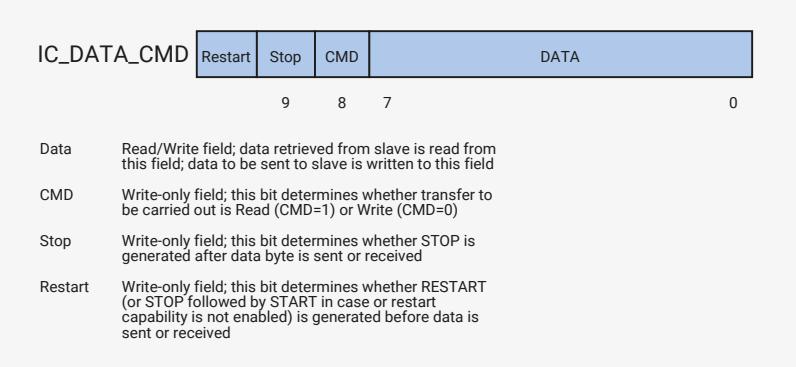
IC_DATA_CMD
| Restart | Stop | CMD | DATA |
| 9 | 8 | 7 | 0 |
Data Read/Write field; data retrieved from slave is read from this field; data to be sent to slave is written to this field
CMD Write-only field; this bit determines whether transfer to be carried out is Read (CMD=1) or Write (CMD=0)
Stop Write-only field; this bit determines whether STOP is generated after data byte is sent or received
Restart Write-only field; this bit determines whether RESTART (or STOP followed by START in case or restart capability is not enabled) is generated before data is sent or received
Figure 73 illustrates the behaviour of the DW_apb_i2c when the Tx FIFO becomes empty while operating as a master transmitter, as well as showing the generation of a STOP condition.
Figure 73. Master Transmitter - Tx FIFO Empties/STOP Generation
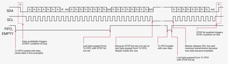
SDA, SCL, FIFO EMPTY
Data availability triggers START condition on bus
Tx FIFO loaded with data (write data in this example)
Last byte popped from Tx FIFO, with STOP bit not set
Because STOP bit was not set on last byte popped from Tx FIFO, Master holds SCL low
Tx FIFO loaded with new data
Master releases SCL line and resumes transmission because new data became available
Last byte popped from Tx FIFO with STOP bit set
STOP bit enabled triggers STOP condition on bus
Figure 74 illustrates the behaviour of the DW_apb_i2c when the Tx FIFO becomes empty while operating as a master receiver, as well as showing the generation of a STOP condition.
Figure 74. Master Receiver - Tx FIFO Empties/STOP Generation
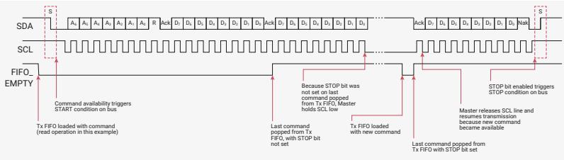
SDA, SCL, FIFO EMPTY
Command availability triggers START condition on bus
Tx FIFO loaded with command (read operation in this example)
Last command popped from Tx FIFO, with STOP bit not set
Because STOP bit was not set on last command popped from Tx FIFO, Master holds SCL low
Tx FIFO loaded with new command
Master releases SCL line and resumes transmission because new command became available
Last command popped from Tx FIFO with STOP bit set
STOP bit enabled triggers STOP condition on bus
Figure 75 and Figure 76 illustrate configurations where the user can control the generation of RESTART conditions on the I2C bus. If bit 10 (Restart) of the IC_DATA_CMD register is set and the restart capability is enabled (IC_RESTART_EN=1), a RESTART is generated before the data byte is written to or read from the slave. If the restart capability is not enabled a STOP followed by a START is generated in place of the RESTART. Figure 75 illustrates this situation during operation as a master transmitter.
Figure 75. Master Transmitter – Restart Bit of IC_DATA_CMD Is Set
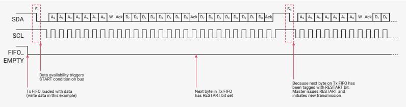
SDA, SCL, FIFO EMPTY
Data availability triggers START condition on bus
Tx FIFO loaded with data (write data in this example)
Next byte in Tx FIFO has RESTART bit set
Because next byte on Tx FIFO has been tagged with RESTART bit, Master issues RESTART and initiates new transmission
Figure 76 illustrates the same situation, but during operation as a master receiver.
Figure 76. Master Receiver – Restart Bit of IC_DATA_CMD Is Set
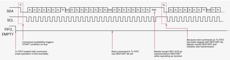
SDA, SCL, FIFO EMPTY
Command availability triggers START condition on bus
Tx FIFO loaded with command (read operation in this example)
Next command in Tx FIFO has RESTART bit set
Master issues NOT ACK as required before RESTART when operating as receiver
Because next command on Tx FIFO has been tagged with RESTART bit, Master issues RESTART and initiates new transmission
Figure 77 illustrates operation as a master transmitter where the Stop bit of the IC_DATA_CMD register is set and the Tx FIFO is not empty
Figure 77. Master Transmitter – Stop Bit of
IC_DATA_CMD
Set/Tx FIFO Not Empty
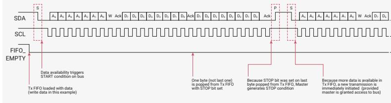
Figure 78 illustrates operation as a master transmitter where the first byte loaded into the Tx FIFO is allowed to go empty with the Restart bit set
Figure 78. Master Transmitter – First Byte Loaded Into Tx FIFO Allowed to Empty, Restart Bit Set
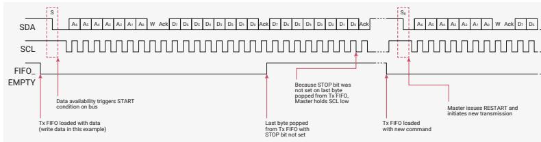
Figure 79 illustrates operation as a master receiver where the Stop bit of the
IC_DATA_CMD
register is set and the Tx FIFO is not empty
Figure 79. Master Receiver – Stop Bit of
IC_DATA_CMD
Set/Tx FIFO Not Empty
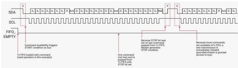
Figure 80 illustrates operation as a master receiver where the first command loaded after the Tx FIFO is allowed to empty and the Restart bit is set
Figure 80. Master Receiver – First Command Loaded After Tx FIFO Allowed to Empty/Restart Bit Set
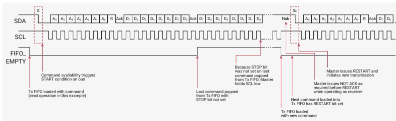
4.3.8. Multiple Master Arbitration
The DW_apb_i2c bus protocol allows multiple masters to reside on the same bus. If there are two masters on the same I2C-bus, there is an arbitration procedure if both try to take control of the bus at the same time by generating a START condition at the same time. Once a master (for example, a microcontroller) has control of the bus, no other master can take control until the first master sends a STOP condition and places the bus in an idle state.
Arbitration takes place on the
SDA
line, while the
SCL
line is one. The master, which transmits a one while the other master transmits zero, loses arbitration and turns off its data output stage. The master that lost arbitration can continue to generate clocks until the end of the byte transfer. If both masters are addressing the same slave device, the arbitration could go into the data phase.
Upon detecting that it has lost arbitration to another master, the DW_apb_i2c will stop generating
SCL
(will disable the output driver). Figure 81 illustrates the timing of when two masters are arbitrating on the bus.
Figure 81. Multiple Master Arbitration
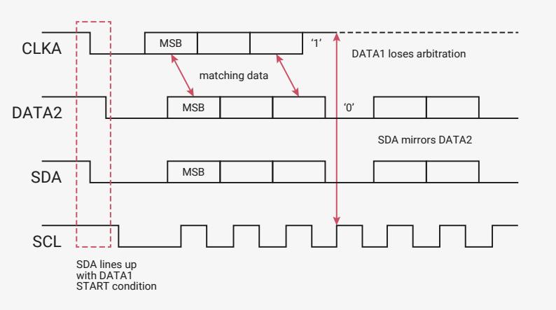
The diagram illustrates the arbitration process on the I2C bus. It shows four signals: CLK_A, DATA2, SDA, and SCL. CLK_A is a square wave. DATA2 and SDA are data lines. SCL is the clock line. A dashed red box highlights the start of the arbitration. SDA lines up with DATA1's START condition. DATA2 and SDA have matching data (MSB) for several clock cycles. At one point, DATA2 has a '1' while SDA has a '0', indicating DATA1 loses arbitration. SDA mirrors DATA2. The SCL signal is a square wave that is high during data transmission and low during arbitration.
Control of the bus is determined by address or master code and data sent by competing masters, so there is no central master nor any order of priority on the bus.
Arbitration is not allowed between the following conditions:
- • A RESTART condition and a data bit
- • A STOP condition and a data bit
- • A RESTART condition and a STOP condition
NOTE
Slaves are not involved in the arbitration process.
4.3.9. Clock Synchronization
When two or more masters try to transfer information on the bus at the same time, they must arbitrate and synchronize the SCL clock. All masters generate their own clock to transfer messages. Data is valid only during the high period of SCL clock. Clock synchronization is performed using the wired-AND connection to the SCL signal. When the master transitions the SCL clock to zero, the master starts counting the low time of the SCL clock and transitions the SCL clock signal to one at the beginning of the next clock period. However, if another master is holding the SCL line to 0, then the master goes into a HIGH wait state until the SCL clock line transitions to one.
All masters then count off their high time, and the master with the shortest high time transitions the SCL line to zero. The masters then count out their low time and the one with the longest low time forces the other masters into a HIGH wait state. Therefore, a synchronized SCL clock is generated, which is illustrated in Figure 82. Optionally, slaves may hold the SCL line low to slow down the timing on the I2C bus.
Figure 82. Multi-Master Clock Synchronization
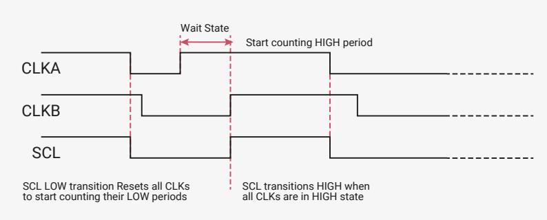
The diagram illustrates the clock synchronization process. It shows three signals: CLK_A, CLK_B, and SCL. CLK_A and CLK_B are master clocks. SCL is the bus clock. A dashed red box highlights the start of the synchronization. SCL LOW transition Resets all CLKs to start counting their LOW periods. SCL transitions HIGH when all CLKs are in HIGH state. A Wait State is shown where one master is holding SCL low while others wait. Start counting HIGH period is indicated when SCL transitions high.
4.3.10. Operation Modes
This section provides information on operation modes.
i NOTE
It is important to note that the DW_apb_i2c should only be set to operate as an I2C Master, or I2C Slave, but not both simultaneously. This is achieved by ensuring that
IC_CON.IC_SLAVE_DISABLE
and
IC_CON.MASTER_MODE
are never set to zero and one, respectively.
4.3.10.1. Slave Mode Operation
This section discusses slave mode procedures.
4.3.10.1.1. Initial Configuration
To use the DW_apb_i2c as a slave, perform the following steps:
- 1. Disable the DW_apb_i2c by writing a '0' to
IC_ENABLE.ENABLE. - 2. Write to the
IC_SARregister (bits 9:0) to set the slave address. This is the address to which the DW_apb_i2c responds. - 3. Write to the
IC_CONregister to specify which type of addressing is supported (7-bit or 10-bit by setting bit 3). Enable the DW_apb_i2c in slave-only mode by writing a '0' into bit six (IC_SLAVE_DISABLE) and a '0' to bit zero (MASTER_MODE).
i NOTE
Slaves and masters do not have to be programmed with the same type of addressing 7-bit or 10-bit address. For instance, a slave can be programmed with 7-bit addressing and a master with 10-bit addressing, and vice versa.
- 1. Enable the DW_apb_i2c by writing a '1' to
IC_ENABLE.ENABLE.
i NOTE
Depending on the reset values chosen, steps two and three may not be necessary because the reset values can be configured. For instance, if the device is only going to be a master, there would be no need to set the slave address because you can configure DW_apb_i2c to have the slave disabled after reset and to enable the master after reset. The values stored are static and do not need to be reprogrammed if the DW_apb_i2c is disabled.
⚠ WARNING
It is recommended that the DW_apb_i2c Slave be brought out of reset only when the I2C bus is IDLE. De-asserting the reset when a transfer is ongoing on the bus causes internal synchronization flip-flops used to synchronize
SDA
and
SCL
to toggle from a reset value of one to the actual value on the bus. This can result in
SDA
toggling from one to zero while
SCL
is one, thereby causing a false START condition to be detected by the DW_apb_i2c Slave. This scenario can also be avoided by configuring the DW_apb_i2c with
IC_SLAVE_DISABLE
= 1 and
MASTER_MODE
= 1 so that the Slave interface is disabled after reset. It can then be enabled by programming
IC_CON[0]
= 0 and
IC_CON[6]
= 0 after the internal
SDA
and
SCL
have synchronized to the value on the bus; this takes approximately six
ic_clk
cycles after reset de-assertion.
4.3.10.1.2. Slave-Transmitter Operation for a Single Byte
When another I2C master device on the bus addresses the DW_apb_i2c and requests data, the DW_apb_i2c acts as a slave-transmitter and the following steps occur:
- 1. The other I2C master device initiates an I2C transfer with an address that matches the slave address in the IC_SAR register of the DW_apb_i2c.
- 2. The DW_apb_i2c acknowledges the sent address and recognizes the direction of the transfer to indicate that it is acting as a slave-transmitter.
- 3. The DW_apb_i2c asserts the RD_REQ interrupt (bit five of the
IC_RAW_INTR_STAT
register) and holds the SCL line low. It is in a wait state until software responds. If the RD_REQ interrupt has been masked, due to
IC_INTR_MASK.M_RD_REQ
being set to zero, then it is recommended that a hardware and/or software timing routine be used to instruct the CPU to perform periodic reads of the
IC_RAW_INTR_STAT
register.
- a. Reads that indicate IC_RAW_INTR_STAT.RD_REQ being set to one must be treated as the equivalent of the RD_REQ interrupt being asserted.
- b. Software must then act to satisfy the I2C transfer.
- c. The timing interval used should be in the order of 10 times the fastest SCL clock period the DW_apb_i2c can handle. For example, for 400kbps, the timing interval is 25µs.
 NOTE
NOTE
The value of 10 is recommended here because this is approximately the amount of time required for a single byte of data transferred on the I2C bus.
- 1. If there is any data remaining in the Tx FIFO before receiving the read request, then the DW_apb_i2c asserts a TX_ABRT interrupt (bit six of the IC_RAW_INTR_STAT register) to flush the old data from the TX FIFO. If the TX_ABRT interrupt has been masked, due to IC_INTR_MASK.M_TX_ABRT being set to zero, then it is recommended that re-using the timing routine (described in the previous step), or a similar one, be used to read the IC_RAW_INTR_STAT register.
 NOTE
NOTE
Because the DW_apb_i2c's Tx FIFO is forced into a flushed/reset state whenever a TX_ABRT event occurs, it is necessary for software to release the DW_apb_i2c from this state by reading the IC_CLR_TX_ABRT register before attempting to write into the Tx FIFO. See register IC_RAW_INTR_STAT for more details.
- a. Reads that indicate bit six ( R_TX_ABRT ) being set to one must be treated as the equivalent of the TX_ABRT interrupt being asserted.
- b. There is no further action required from software.
- c. The timing interval used should be similar to that described in the previous step for the
IC_RAW_INTR_STAT.RD_REQ
register.
- 1. Software writes to the IC_DATA_CMD register with the data to be written (by writing a '0' in bit 8).
- 2. Software must clear the RD_REQ and TX_ABRT interrupts (bits five and six, respectively) of the IC_RAW_INTR_STAT register before proceeding. If the RD_REQ and/or TX_ABRT interrupts have been masked, then clearing of the IC_RAW_INTR_STAT register will have already been performed when either the R_RD_REQ or R_TX_ABRT bit has been read as one.
- 3. The DW_apb_i2c releases the SCL and transmits the byte.
- 4. The master may hold the I2C bus by issuing a RESTART condition or release the bus by issuing a STOP condition.
Slave-Transmitter Operation for a Single Byte is not applicable in Ultra-Fast Mode as Read transfers are not supported.
4.3.10.1.3. Slave-Receiver Operation for a Single ByteWhen another I2C master device on the bus addresses the DW_apb_i2c and is sending data, the DW_apb_i2c acts as a slave-receiver and the following steps occur:
- 1. The other I2C master device initiates an I2C transfer with an address that matches the DW_apb_i2c's slave address in the IC_SAR register.
- 2. The DW_apb_i2c acknowledges the sent address and recognizes the direction of the transfer to indicate that the DW_apb_i2c is acting as a slave-receiver.
- 3. DW_apb_i2c receives the transmitted byte and places it in the receive buffer.
If the Rx FIFO is completely filled with data when a byte is pushed, then the DW_apb_i2c slave holds the I2C SCL line low until the Rx FIFO has some space, and then continues with the next read request.
- 1. DW_apb_i2c asserts the RX_FULL interrupt IC_RAW_INTR_STAT.RX_FULL . If the RX_FULL interrupt has been masked, due to setting IC_INTR_MASK.M_RX_FULL register to zero or setting IC_TX_TL to a value larger than zero, then it is recommended that a timing routine (described in Section 4.3.10.1.2 ) be implemented for periodic reads of the IC_STATUS register. Reads of the IC_STATUS register, with bit 3 (RFNE) set at one, must then be treated by software as the equivalent of the RX_FULL interrupt being asserted.
- 2. Software may read the byte from the IC_DATA_CMD register (bits 7:0).
- 3. The other master device may hold the I2C bus by issuing a RESTART condition, or release the bus by issuing a STOP condition.
In the standard I2C protocol, all transactions are single byte transactions and the programmer responds to a remote master read request by writing one byte into the slave's TX FIFO. When a slave (slave-transmitter) is issued with a read request (RD_REQ) from the remote master (master-receiver), at a minimum there should be at least one entry placed into the slave-transmitter's TX FIFO. DW_apb_i2c is designed to handle more data in the TX FIFO so that subsequent read requests can take that data without raising an interrupt to get more data. Ultimately, this eliminates the possibility of significant latencies being incurred between raising the interrupt for data each time had there been a restriction of having only one entry placed in the TX FIFO. This mode only occurs when DW_apb_i2c is acting as a slave-transmitter. If the remote master acknowledges the data sent by the slave-transmitter and there is no data in the slave's TX FIFO, the DW_apb_i2c holds the I2C SCL line low while it raises the read request interrupt (RD_REQ) and waits for data to be written into the TX FIFO before it can be sent to the remote master.
If the RD_REQ interrupt is masked, due to IC_INTR_STAT.R_RD_REQ set to zero, then it is recommended that a timing routine be used to activate periodic reads of the IC_RAW_INTR_STAT register. Reads of IC_RAW_INTR_STAT that return bit five (RD_REQ) set to one must be treated as the equivalent of the RD_REQ interrupt referred to in this section. This timing routine is similar to that described in Section 4.3.10.1.2 .
The RD_REQ interrupt is raised upon a read request, and like interrupts, must be cleared when exiting the interrupt service handling routine (ISR). The ISR allows you to either write one byte or more than one byte into the Tx FIFO. During the transmission of these bytes to the master, if the master acknowledges the last byte, then the slave must raise the RD_REQ again because the master is requesting for more data. If the programmer knows in advance that the remote master is requesting a packet of 'n' bytes, then when another master addresses DW_apb_i2c and requests data, the Tx FIFO could be written with 'n' bytes and the remote master receives it as a continuous stream of data. For example, the
DW_apb_i2c slave continues to send data to the remote master as long as the remote master is acknowledging the data sent and there is data available in the Tx FIFO. There is no need to hold the SCL line low or to issue RD_REQ again.
If the remote master is to receive 'n' bytes from the DW_apb_i2c but the programmer wrote a number of bytes larger than 'n' to the Tx FIFO, then when the slave finishes sending the requested 'n' bytes, it clears the Tx FIFO and ignores any excess bytes.
The DW_apb_i2c generates a transmit abort (TX_ABRT) event to indicate the clearing of the Tx FIFO in this example. At the time an ACK/NACK is expected, if a NACK is received, then the remote master has all the data it wants. At this time, a flag is raised within the slave's state machine to clear the leftover data in the Tx FIFO. This flag is transferred to the processor bus clock domain where the FIFO exists and the contents of the Tx FIFO is cleared at that time.
4.3.10.2. Master Mode Operation
This section discusses master mode procedures.
4.3.10.2.1. Initial Configuration
To use the DW_apb_i2c as a master perform the following steps:
- 1. Disable the DW_apb_i2c by writing zero to IC_ENABLE.ENABLE .
- 2. Write to the IC_CON register to set the maximum speed mode supported (bits 2:1) and the desired speed of the DW_apb_i2c master-initiated transfers, either 7-bit or 10-bit addressing (bit 4). Ensure that bit six ( IC_SLAVE_DISABLE ) is written with a '1' and bit zero ( MASTER_MODE ) is written with a '1'.
Note: Slaves and masters do not have to be programmed with the same type of 7-bit or 10-bit address. For instance, a slave can be programmed with 7-bit addressing and a master with 10-bit addressing, and vice versa.
- 1. Write to the IC_TAR register the address of the I2C device to be addressed (bits 9:0). This register also indicates whether a General Call or a START BYTE command is going to be performed by I2C.
- 2. Enable the DW_apb_i2c by writing a one to IC_ENABLE.ENABLE .
- 3. Now write transfer direction and data to be sent to the IC_DATA_CMD register. If the IC_DATA_CMD register is written before the DW_apb_i2c is enabled, the data and commands are lost as the buffers are kept cleared when DW_apb_i2c is disabled. This step generates the START condition and the address byte on the DW_apb_i2c. Once DW_apb_i2c is enabled and there is data in the TX FIFO, DW_apb_i2c starts reading the data.
i NOTE
Depending on the reset values chosen, steps two, three, four, and five may not be necessary because the reset values can be configured. The values stored are static and do not need to be reprogrammed if the DW_apb_i2c is disabled, with the exception of the transfer direction and data.
4.3.10.2.2. Master Transmit and Master Receive
The DW_apb_i2c supports switching back and forth between reading and writing dynamically. To transmit data, write the data to be written to the lower byte of the I2C Rx/Tx Data Buffer and Command Register ( IC_DATA_CMD ). The CMD bit [8] should be written to zero for I2C write operations. Subsequently, a read command may be issued by writing "don't cares" to the lower byte of the IC_DATA_CMD register, and a one should be written to the CMD bit. The DW_apb_i2c master continues to initiate transfers as long as there are commands present in the transmit FIFO. If the transmit FIFO becomes empty the master either inserts a STOP condition after completing the current transfers.
- • If set to one, it issues a STOP condition after completing the current transfer.
- • If set to zero, it holds SCL low until next command is written to the transmit FIFO.
For more details, refer to Section 4.3.7 .
4.3.10.3. Disabling DW_apb_i2c
The register
IC_ENABLE_STATUS
is added to allow software to unambiguously determine when the hardware has completely shutdown in response to
IC_ENABLE.ENABLE
being set from one to zero.
Only one register is required to be monitored, as opposed to monitoring two registers (
IC_STATUS
and
IC_RAW_INTR_STAT
) which was a requirement for earlier versions of DW_apb_i2c.
Image: info icon
NOTEThe DW_apb_i2c Master can be disabled only if the current command being processed—when the
ic_enable
de-assertion occurs—has the STOP bit set to one. When an attempt is made to disable the DW_apb_i2c Master while processing a command without the STOP bit set, the DW_apb_i2c Master continues to remain active, holding the
SCL
line low until a new command is received in the Tx FIFO. When the DW_apb_i2c Master is processing a command without the STOP bit set, you can issue the ABORT (
IC_ENABLE.ABORT
) to relinquish the I2C bus and then disable DW_apb_i2c.
4.3.10.3.1. Procedure
- 1. Define a timer interval ( \( t_{i2c\_poll} \) ) equal to the 10 times the signalling period for the highest I2C transfer speed used in the system and supported by DW_apb_i2c. For example, if the highest I2C transfer mode is 400kbps, then this \( t_{i2c\_poll} \) is 25 \( \mu s \) .
- 2. Define a maximum time-out parameter,
MAX_T_POLL_COUNT, such that if any repeated polling operation exceeds this maximum value, an error is reported. - 3. Execute a blocking thread/process/function that prevents any further I2C master transactions to be started by software, but allows any pending transfers to be completed.
Image: info icon
NOTEThis step can be ignored if DW_apb_i2c is programmed to operate as an I2C slave only.
- 1. The variable
POLL_COUNTis initialized to zero. - 2. Set bit zero of the
IC_ENABLEregister to zero. - 3. Read the
IC_ENABLE_STATUSregister and test theIC_ENbit (bit 0). IncrementPOLL_COUNTby one. IfPOLL_COUNT >= MAX_T_POLL_COUNT, exit with the relevant error code. - 4. If
IC_ENABLE_STATUS[0]is one, then sleep for \( t_{i2c\_poll} \) and proceed to the previous step. Otherwise, exit with a relevant success code.
4.3.10.4. Aborting I2C Transfers
The ABORT control bit of the
IC_ENABLE
register allows the software to relinquish the I2C bus before completing the issued transfer commands from the Tx FIFO. In response to an ABORT request, the controller issues the STOP condition over the I2C bus, followed by Tx FIFO flush. Aborting the transfer is allowed only in master mode of operation.
4.3.10.4.1. Procedure
- 1. Stop filling the Tx FIFO (
IC_DATA_CMD) with new commands. - 2. When operating in DMA mode, disable the transmit DMA by setting
TDMAEto zero. - 3. Set
IC_ENABLE.ABORTto one. - 4. Wait for the
M_TX_ABORTinterrupt.
- 5. Read the
IC_TX_ABRT_SOURCEregister to identify the source asABRT_USER_ABRT.
4.3.11. Spike Suppression
The
DW_apb_i2c
contains programmable spike suppression logic that match requirements imposed by the I2C Bus Specification for SS/FS modes. This logic is based on counters that monitor the input signals (
SCL
and
SDA
), checking if they remain stable for a predetermined amount of
ic_clk
cycles before they are sampled internally. There is one separate counter for each signal (
SCL
and
SDA
). The number of
ic_clk
cycles can be programmed by the user and should be calculated taking into account the frequency of
ic_clk
and the relevant spike length specification. Each counter is started whenever its input signal changes its value. Depending on the behaviour of the input signal, one of the following scenarios occurs:
- • The input signal remains unchanged until the counter reaches its count limit value. When this happens, the internal version of the signal is updated with the input value, and the counter is reset and stopped. The counter is not restarted until a new change on the input signal is detected.
- • The input signal changes again before the counter reaches its count limit value. When this happens, the counter is reset and stopped, but the internal version of the signal is not updated. The counter remains stopped until a new change on the input signal is detected.
The timing diagram in Figure 83 illustrates the behaviour described above.
Figure 83. Spike Suppression Example
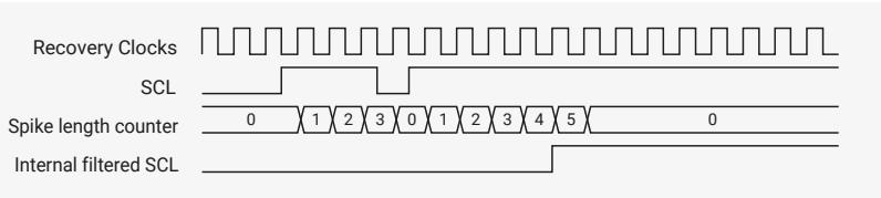
The diagram shows four signals over time:
- Recovery Clocks: A periodic square wave.
- SCL: A signal that transitions from low to high, then back to low, then high again. It has a spike (a short high pulse) during the first high period.
- Spike length counter: A counter that starts at 0 when SCL transitions from low to high. It increments to 1, 2, 3, 0, 1, 2, 3, 4, 5, and then resets to 0. The counter stops at 5 when SCL transitions from high to low.
- Internal filtered SCL: A signal that is low until the counter reaches 5, then it becomes high and remains high until the next SCL transition.
NOTE
There is a 2-stage synchronizer on the
SCL
input, but for the sake of simplicity this synchronization delay was not included in the timing diagram in
Figure 83
.
The I2C Bus Specification calls for different maximum spike lengths according to the operating mode – 50ns for SS and FS, so this register is required to store the values needed:
- • Register
IC_FS_SPKLENholds the maximum spike length for SS and FS modes
This register is 8 bits wide and accessible through the APB interface for read and write purposes; however, they can be written to only when the
DW_apb_i2c
is disabled. The minimum value that can be programmed into these registers is one; attempting to program a value smaller than one results in the value one being written.
The default value for these registers is based on the value of 100ns for
ic_clk
period, so should be updated for the
clk_sys
period in use on RP2040.
- • Because the minimum value that can be programmed into the
IC_FS_SPKLENregister is one, the spike length specification can be exceeded for low frequencies ofic_clk. Consider the simple example of a 10MHz (100ns period)ic_clk; in this case, the minimum spike length that can be programmed is 100ns, which means that spikes up to this length are suppressed. - • Standard synchronization logic (two flip-flops in series) is implemented upstream of the spike suppression logic and is not affected in any way by the contents of the spike length registers or the operation of the spike suppression logic; the two operations (synchronization and spike suppression) are completely independent. Because the
SCLandSDAinputs are asynchronous toic_clk, there is oneic_clkcycle uncertainty in the sampling of these signals; that is, depending on when they occur relative to the rising edge ofic_clk, spikes of the same original length might show a difference of oneic_clkcycle after being sampled. - • Spike suppression is symmetrical; that is, the behaviour is exactly the same for transitions from zero to one and from one to zero.
4.3.12. Fast Mode Plus Operation
In fast mode plus, the
DW_apb_i2c
allows the fast mode operation to be extended to support speeds up to 1000kbps. To enable the
DW_apb_i2c
for fast mode plus operation, perform the following steps before initiating any data transfer:
- 1. Set
ic_clkfrequency greater than or equal to 32MHz (refer to Section 4.3.14.2.1 ). - 2. Program the
IC_CONregister [2:1] = 2'b10 for fast mode or fast mode plus. - 3. Program
IC_FS_SCL_LCNTandIC_FS_SCL_HCNTregisters to meet the fast mode plusSCL(refer to Section 4.3.14 ). - 4. Program the
IC_FS_SPKLENregister to suppress the maximum spike of 50ns. - 5. Program the
IC_SDA_SETUPregister to meet the minimum data setup time (tSU; DAT).
4.3.13. Bus Clear Feature
DW_apb_i2c
supports the bus clear feature that provides graceful recovery of data
SDA
and clock
SCL
lines during unlikely events in which either the clock or data line is stuck at LOW.
4.3.13.1. SDA Line Stuck at LOW Recovery
In case of
SDA
line stuck at LOW, the master performs the following actions to recover as shown in
Figure 84
and
Figure 85
:
- 1. Master sends a maximum of nine clock pulses to recover the bus LOW within those nine clocks.
- ◦ The number of clock pulses will vary with the number of bits that remain to be sent by the slave. As the maximum number of bits is nine, master sends up to nine clock pulses and allows the slave to recover it.
- ◦ The master attempts to assert a Logic 1 on the
SDAline and check whetherSDAis recovered. If theSDAis not recovered, it will continue to send a maximum of nineSCLclocks.
- 2. If
SDAline is recovered within nine clock pulses then the master will send the STOP to release the bus. - 3. If
SDAline is not recovered even after the ninth clock pulse then system needs a hardware reset.
Figure 84. SDA Recovery with 9 SCL Clocks

Recovery Clocks 0 1 2 3 4 5 6 7 8 9 10
SCL
SDA
MST_SDA
Master drives 9 clocks to recover SDA stuck at low
Figure 85. SDA Recovery with 6 SCL Clocks
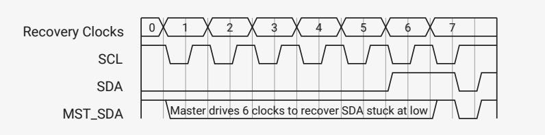
Recovery Clocks 0 1 2 3 4 5 6 7
SCL
SDA
MST_SDA
Master drives 6 clocks to recover SDA stuck at low
4.3.13.2. SCL Line is Stuck at LOW
In the unlikely event (due to an electric failure of a circuit) where the clock (SCL) is stuck to LOW, there is no effective method to overcome this problem but to reset the bus using the hardware reset signal.
4.3.14. IC_CLK Frequency Configuration
When the DW_apb_i2c is configured as a Standard (SS), Fast (FS)/Fast-Mode Plus (FM+), the *CNT registers must be set before any I2C bus transaction can take place in order to ensure proper I/O timing. The *CNT registers are:
- • IC_SS_SCL_HCNT
- • IC_SS_SCL_LCNT
- • IC_FS_SCL_HCNT
- • IC_FS_SCL_LCNT
i NOTE
The tBUF timing and setup/hold time of START, STOP and RESTART registers uses *HCNT/*LCNT register settings for the corresponding speed mode.
i NOTE
It is not necessary to program any of the *CNT registers if the DW_apb_i2c is enabled to operate only as an I2C slave, since these registers are used only to determine the SCL timing requirements for operation as an I2C master.
Table 449 lists the derivation of I2C timing parameters from the *CNT programming registers.
Table 449. Derivation of I2C Timing Parameters from *CNT Registers
| Timing Parameter | Symbol | Standard Speed | Fast Speed / Fast Speed Plus |
|---|---|---|---|
| LOW period of the SCL clock | tLOW | IC_SS_SCL_LCNT | IC_FS_SCL_LCNT |
| HIGH period of the SCL clock | tHIGH | IC_SS_SCL_HCNT | IC_FS_SCL_HCNT |
| Setup time for a repeated START condition | tSU;STA | IC_SS_SCL_LCNT | IC_FS_SCL_HCNT |
| Hold time (repeated) START condition* | tHD;STA | IC_SS_SCL_HCNT | IC_FS_SCL_HCNT |
| Setup time for STOP condition | tSU;STO | IC_SS_SCL_HCNT | IC_FS_SCL_HCNT |
| Timing Parameter | Symbol | Standard Speed | Fast Speed / Fast Speed Plus |
|---|---|---|---|
| Bus free time between a STOP and a START condition | tBUF | IC_SS_SCL_LCNT | IC_FS_SCL_LCNT |
| Spike length | tSP | IC_FS_SPKLEN | IC_FS_SPKLEN |
| Data hold time | tHD;DAT | IC_SDA_HOLD | IC_SDA_HOLD |
| Data setup time | tSU;DAT | IC_SDA_SETUP | IC_SDA_SETUP |
4.3.14.1. Minimum High and Low Counts in SS, FS, and FM+ Modes.
When the DW_apb_i2c operates as an I2C master, in both transmit and receive transfers:
- • IC_SS_SCL_LCNT and IC_FS_SCL_LCNT register values must be larger than IC_FS_SPKLEN + 7.
- • IC_SS_SCL_HCNT and IC_FS_SCL_HCNT register values must be larger than IC_FS_SPKLEN + 5.
Details regarding the DW_apb_i2c high and low counts are as follows:
- • The minimum value of IC_*_SPKLEN + 7 for the *_LCNT registers is due to the time required for the DW_apb_i2c to drive SDA after a negative edge of SCL.
- • The minimum value of IC_*_SPKLEN + 5 for the *_HCNT registers is due to the time required for the DW_apb_i2c to sample SDA during the high period of SCL.
- • The DW_apb_i2c adds one cycle to the programmed *_LCNT value in order to generate the low period of the SCL clock; this is due to the counting logic for SCL low counting to (*_LCNT + 1).
- • The DW_apb_i2c adds IC_*_SPKLEN + 7 cycles to the programmed *_HCNT value in order to generate the high period of the SCL clock; this is due to the following factors:
- ◦ The counting logic for SCL high counts to (*_HCNT+1).
- ◦ The digital filtering applied to the SCL line incurs a delay of SPKLEN + 2 ic_clk cycles, where SPKLEN is:
- ▪ IC_FS_SPKLEN if the component is operating in SS or FS
- ◦ Whenever SCL is driven one to zero by the DW_apb_i2c—that is, completing the SCL high time—an internal logic latency of three ic_clk cycles is incurred. Consequently, the minimum SCL low time of which the DW_apb_i2c is capable is nine ic_clk periods (7 + 1 + 1), while the minimum SCL high time is thirteen ic_clk periods (6 + 1 + 3 + 3).
i NOTE
The total high time and low time of SCL generated by the DW_apb_i2c master is also influenced by the rise time and fall time of the SCL line, as shown in the illustration and equations in Figure 86. It should be noted that the SCL rise and fall time parameters vary, depending on external factors such as:
- • Characteristics of IO driver
- • Pull-up resistor value
- • Total capacitance on SCL line, and so on
These characteristics are beyond the control of the DW_apb_i2c.
Figure 86. Impact of SCL Rise Time and Fall Time on Generated SCL
![Timing diagram showing the impact of SCL rise and fall times on the generated SCL signal. The diagram shows two waveforms: ic_clk (clock) and ic_clk_in_a/SCL (SCL signal). The SCL signal is a square wave that is delayed and distorted by the rise and fall times of the ic_clk signal. The diagram labels the SCL rise time, SCL fall time, and the high and low pulse widths. The high pulse width is labeled as HCNT + IC_*_SPKLEN + 7, and the low pulse width is labeled as LCNT + 1. The diagram also includes the following equations: SCL_High_time = [(HCNT + IC_*_SPKLEN + 7) * ic_clk] + SCL_Fall_time and SCL_Low_time = [(LCNT + 1) * ic_clk] - SCL_Fall_time + SCL_Rise_time.](/RP2040/b2e7b89d143594af5af2d3dc1bb2cbff_img.jpg)
ic_clk
ic_clk_in_a/SCL
SCL rise time
HCNT + IC_*_SPKLEN + 7
SCL fall time
LCNT + 1
SCL rise time
SCL_High_time = [(HCNT + IC_*_SPKLEN + 7) * ic_clk] + SCL_Fall_time
SCL_Low_time = [(LCNT + 1) * ic_clk] - SCL_Fall_time + SCL_Rise_time
4.3.14.2. Minimum IC_CLK Frequency
This section describes the minimum ic_clk frequencies that the DW_apb_i2c supports for each speed mode, and the associated high and low count values. In Slave mode, IC_SDA_HOLD (Thd;dat) and IC_SDA_SETUP (Tsu;dat) need to be programmed to satisfy the I2C protocol timing requirements. The following examples are for the case where IC_FS_SPKLEN is programmed to two.
4.3.14.2.1. Standard Mode (SM), Fast Mode (FM), and Fast Mode Plus (FM+)
This section details how to derive a minimum ic_clk value for standard and fast modes of the DW_apb_i2c. Although the following method shows how to do fast mode calculations, you can also use the same method in order to do calculations for standard mode and fast mode plus.
NOTE
The following computations do not consider the SCL_Rise_time and SCL_Fall_time.
Given conditions and calculations for the minimum DW_apb_i2c ic_clk value in fast mode:
- Fast mode has data rate of 400kbps; implies SCL period of 1/400kHz = 2.5μs
- Minimum hcnt value of 14 as a seed value; IC_HCNT_FS = 14
- Protocol minimum
SCL
high and low times:
- MIN_SCL_LOWtime_FS = 1300ns
- MIN_SCL_HIGHtime_FS = 600ns
Derived equations:
Combined, the previous equations produce the following:
Solving for IC_LCNT_FS:
The previous equation gives:
These calculations produce \( IC\_LCNT\_FS = 16 \) and \( IC\_HCNT\_FS = 14 \) , giving an \( ic\_clk \) value of:
Testing these results shows that protocol requirements are satisfied.
Table 450 lists the minimum \( ic\_clk \) values for all modes with high and low count values.
Table 450. \( ic\_clk \) in Relation to High and Low Counts
| Speed Mode | \( ic\_clk \) freq (MHz) | Minimum Value of \( IC\_*_SPKLEN \) | SCL Low Time in ' \( ic\_clk \) 's | SCL Low Program Value | SCL Low Time | SCL High Time in ' \( ic\_clk \) 's | SCL High Program Value | SCL High Time |
|---|---|---|---|---|---|---|---|---|
| SS | 2.7 | 1 | 13 | 12 | 4.7 \( \mu s \) | 14 | 6 | 5.2 \( \mu s \) |
| FS | 12.0 | 1 | 16 | 15 | 1.33 \( \mu s \) | 14 | 6 | 1.16 \( \mu s \) |
| FM+ | 32 | 2 | 16 | 15 | 500ns | 16 | 7 | 500ns |
- The \( IC\_*_SCL\_LCNT \) and \( IC\_*_SCL\_HCNT \) registers are programmed using the SCL low and high program values in Table 450, which are calculated using SCL low count minus one, and SCL high counts minus eight, respectively. The values in Table 450 are based on \( IC\_SDA\_RX\_HOLD = 0 \) . The maximum \( IC\_SDA\_RX\_HOLD \) value depends on the \( IC\_*CNT \) registers in Master mode.
- In order to compute the HCNT and LCNT considering RC timings, use the following equations:
- \( IC\_HCNT\_* = [(HCNT + IC\_*_SPKLEN + 7) * ic\_clk] + SCL\_Fall\_time \)
- \( IC\_LCNT\_* = [(LCNT + 1) * ic\_clk] - SCL\_Fall\_time + SCL\_Rise\_time \)
4.3.14.3. Calculating High and Low Counts
The calculations below show how to calculate SCL high and low counts for each speed mode in the DW_apb_i2c. For the calculations to work, the \( ic\_clk \) frequencies used must not be less than the minimum \( ic\_clk \) frequencies specified in Table 450.
The default \( ic\_clk \) period value is set to 100ns, so default SCL high and low count values are calculated for each speed mode based on this clock. These values need updating according to the guidelines below.
The equation to calculate the proper number of \( ic\_clk \) signals required for setting the proper SCL clocks high and low times is as follows:
MIN_SCL_HIGHTime = Minimum High Period
MIN_SCL_HIGHTime = 4000ns for 100kbps,
600ns for 400kbps,
260ns for 1000kbps,
MIN_SCL_LOWtime = Minimum Low Period
MIN_SCL_LOWtime = 4700ns for 100kbps,
1300ns for 400kbps,
500ns for 1000kbps,

OSCFREQ = ic_clk Clock Frequency (Hz).
For example:
OSCFREQ = 100MHz
I2Cmode = fast, 400kbps
MIN_SCL_HIGHTime = 600ns.
MIN_SCL_LOWtime = 1300ns.

IC_xCNT = (ROUNDUP(MIN_SCL_HIGH_LOWtime*OSCFREQ,0))

IC_HCNT = (ROUNDUP(600ns * 100MHz,0))
IC_HCNTSCL PERIOD = 60
IC_LCNT = (ROUNDUP(1300ns * 100MHz,0))
IC_LCNTSCL PERIOD = 130
Actual MIN_SCL_HIGHTime = 60*(1/100MHz) = 600ns
Actual MIN_SCL_LOWtime = 130*(1/100MHz) = 1300ns
4.3.15. DMA Controller Interface
The DW_apb_i2c has built-in DMA capability; it has a handshaking interface to the DMA Controller to request and control transfers. The APB bus is used to perform the data transfer to or from the DMA. DMA transfers are transferred as single accesses as data rate is relatively low.
4.3.15.1. Enabling the DMA Controller Interface
To enable the DMA Controller interface on the DW_apb_i2c, you must write the DMA Control Register ( IC_DMA_CR ). Writing a one into the TDMAE bit field of IC_DMA_CR register enables the DW_apb_i2c transmit handshaking interface. Writing a one into the RDMAE bit field of the IC_DMA_CR register enables the DW_apb_i2c receive handshaking interface.
4.3.15.2. Overview of Operation
The DMA Controller is programmed with the number of data items (transfer count) that are to be transmitted or received by DW_apb_i2c.
The transfer is broken into single transfers on the bus, each initiated by a request from the DW_apb_i2c.
For example, where the transfer count programmed into the DMA Controller is four. The DMA transfer consists of a series of four single transactions. If the DW_apb_i2c makes a transmit request to this channel, a single data item is written to the DW_apb_i2c TX FIFO. Similarly, if the DW_apb_i2c makes a receive request to this channel, a single data item is read from the DW_apb_i2c RX FIFO. Four separate requests must be made to this DMA channel before all four data items are written or read.
4.3.15.3. Watermark Levels
In DW_apb_i2c the registers for setting watermarks to allow DMA bursts do not need be set to anything other than their reset value. Specifically IC_DMA_TDLR and IC_DMA_RDLR can be left at reset values of zero. This is because only single transfers are needed due to the low bandwidth of I2C relative to system bandwidth, and also the DMA controller
normally has highest priority on the system bus so will generally complete very quickly.
4.3.16. Operation of Interrupt Registers
Table 451 lists the operation of the DW_apb_i2c interrupt registers and how they are set and cleared. Some bits are set by hardware and cleared by software, whereas other bits are set and cleared by hardware.
Table 451. Clearing and Setting of Interrupt Registers
| Interrupt Bit Fields | Set by Hardware/Cleared by Software | Set and Cleared by Hardware |
|---|---|---|
| RESTART_DET | Y | N |
| GEN_CALL | Y | N |
| START_DET | Y | N |
| STOP_DET | Y | N |
| ACTIVITY | Y | N |
| RX_DONE | Y | N |
| TX_ABRT | Y | N |
| RD_REQ | Y | N |
| TX_EMPTY | N | Y |
| TX_OVER | Y | N |
| RX_FULL | N | Y |
| RX_OVER | Y | N |
| RX_UNDER | Y | N |
4.3.17. List of Registers
The I2C0 and I2C1 registers start at base addresses of 0x40044000 and 0x40048000 respectively (defined as I2C0_BASE and I2C1_BASE in SDK).
NOTE
You may see references to configuration constants in the I2C register descriptions; these are fixed values, set at hardware design time. A full list of their values can be found in https://github.com/raspberrypi/pico-sdk/blob/master/src/rp2040/hardware_regs/include/hardware/regs/i2c.h
Table 452. List of I2C registers
| Offset | Name | Info |
|---|---|---|
| 0x00 | IC_CON | I2C Control Register |
| 0x04 | IC_TAR | I2C Target Address Register |
| 0x08 | IC_SAR | I2C Slave Address Register |
| 0x10 | IC_DATA_CMD | I2C Rx/Tx Data Buffer and Command Register |
| 0x14 | IC_SS_SCL_HCNT | Standard Speed I2C Clock SCL High Count Register |
| 0x18 | IC_SS_SCL_LCNT | Standard Speed I2C Clock SCL Low Count Register |
| 0x1c | IC_FS_SCL_HCNT | Fast Mode or Fast Mode Plus I2C Clock SCL High Count Register |
| 0x20 | IC_FS_SCL_LCNT | Fast Mode or Fast Mode Plus I2C Clock SCL Low Count Register |
| Offset | Name | Info |
|---|---|---|
| 0x2c | IC_INTR_STAT | I2C Interrupt Status Register |
| 0x30 | IC_INTR_MASK | I2C Interrupt Mask Register |
| 0x34 | IC_RAW_INTR_STAT | I2C Raw Interrupt Status Register |
| 0x38 | IC_RX_TL | I2C Receive FIFO Threshold Register |
| 0x3c | IC_TX_TL | I2C Transmit FIFO Threshold Register |
| 0x40 | IC_CLR_INTR | Clear Combined and Individual Interrupt Register |
| 0x44 | IC_CLR_RX_UNDER | Clear RX_UNDER Interrupt Register |
| 0x48 | IC_CLR_RX_OVER | Clear RX_OVER Interrupt Register |
| 0x4c | IC_CLR_TX_OVER | Clear TX_OVER Interrupt Register |
| 0x50 | IC_CLR_RD_REQ | Clear RD_REQ Interrupt Register |
| 0x54 | IC_CLR_TX_ABRT | Clear TX_ABRT Interrupt Register |
| 0x58 | IC_CLR_RX_DONE | Clear RX_DONE Interrupt Register |
| 0x5c | IC_CLR_ACTIVITY | Clear ACTIVITY Interrupt Register |
| 0x60 | IC_CLR_STOP_DET | Clear STOP_DET Interrupt Register |
| 0x64 | IC_CLR_START_DET | Clear START_DET Interrupt Register |
| 0x68 | IC_CLR_GEN_CALL | Clear GEN_CALL Interrupt Register |
| 0x6c | IC_ENABLE | I2C ENABLE Register |
| 0x70 | IC_STATUS | I2C STATUS Register |
| 0x74 | IC_TXFLR | I2C Transmit FIFO Level Register |
| 0x78 | IC_RXFLR | I2C Receive FIFO Level Register |
| 0x7c | IC_SDA_HOLD | I2C SDA Hold Time Length Register |
| 0x80 | IC_TX_ABRT_SOURCE | I2C Transmit Abort Source Register |
| 0x84 | IC_SLV_DATA_NACK_ONLY | Generate Slave Data NACK Register |
| 0x88 | IC_DMA_CR | DMA Control Register |
| 0x8c | IC_DMA_TDLR | DMA Transmit Data Level Register |
| 0x90 | IC_DMA_RDLR | DMA Transmit Data Level Register |
| 0x94 | IC_SDA_SETUP | I2C SDA Setup Register |
| 0x98 | IC_ACK_GENERAL_CALL | I2C ACK General Call Register |
| 0x9c | IC_ENABLE_STATUS | I2C Enable Status Register |
| 0xa0 | IC_FS_SPKLEN | I2C SS, FS or FM+ spike suppression limit |
| 0xa8 | IC_CLR_RESTART_DET | Clear RESTART_DET Interrupt Register |
| 0xf4 | IC_COMP_PARAM_1 | Component Parameter Register 1 |
| 0xf8 | IC_COMP_VERSION | I2C Component Version Register |
| 0xfc | IC_COMP_TYPE | I2C Component Type Register |
I2C: IC_CON Register
Offset: 0x00
DescriptionI2C Control Register. This register can be written only when the DW_apb_i2c is disabled, which corresponds to the IC_ENABLE[0] register being set to 0. Writes at other times have no effect.
Read/Write Access: - bit 10 is read only. - bit 11 is read only - bit 16 is read only - bit 17 is read only - bits 18 and 19 are read only.
Table 453. IC_CON Register
| Bits | Description | Type | Reset |
|---|---|---|---|
| 31:11 | Reserved. | - | - |
| 10 | STOP_DET_IF_MASTER_ACTIVE : Master issues the STOP_DET interrupt irrespective of whether master is active or not | RO | 0x0 |
| 9 | RX_FIFO_FULL_HLD_CTRL
: This bit controls whether DW_apb_i2c should hold the bus when the Rx FIFO is physically full to its RX_BUFFER_DEPTH, as described in the IC_RX_FULL_HLD_BUS_EN parameter. Reset value: 0x0. | RW | 0x0 |
| Enumerated values: | |||
| 0x0 → DISABLED: Overflow when RX_FIFO is full | |||
| 0x1 → ENABLED: Hold bus when RX_FIFO is full | |||
| 8 | TX_EMPTY_CTRL
: This bit controls the generation of the TX_EMPTY interrupt, as described in the IC_RAW_INTR_STAT register. Reset value: 0x0. | RW | 0x0 |
| Enumerated values: | |||
| 0x0 → DISABLED: Default behaviour of TX_EMPTY interrupt | |||
| 0x1 → ENABLED: Controlled generation of TX_EMPTY interrupt | |||
| 7 | STOP_DET_IFADDRESSED
: In slave mode: - 1'b1: issues the STOP_DET interrupt only when it is addressed. - 1'b0: issues the STOP_DET irrespective of whether it's addressed or not. Reset value: 0x0 NOTE: During a general call address, this slave does not issue the STOP_DET interrupt if STOP_DET_IF_ADDRESSED = 1'b1, even if the slave responds to the general call address by generating ACK. The STOP_DET interrupt is generated only when the transmitted address matches the slave address (SAR). | RW | 0x0 |
| Enumerated values: | |||
| 0x0 → DISABLED: slave issues STOP_DET intr always | |||
| 0x1 → ENABLED: slave issues STOP_DET intr only if addressed | |||
| 6 | IC_SLAVE_DISABLE
: This bit controls whether I2C has its slave disabled, which means once the preseln signal is applied, then this bit is set and the slave is disabled. If this bit is set (slave is disabled), DW_apb_i2c functions only as a master and does not perform any action that requires a slave. NOTE: Software should ensure that if this bit is written with 0, then bit 0 should also be written with a 0. | RW | 0x1 |
| Bits | Description | Type | Reset |
|---|---|---|---|
| Enumerated values: | |||
| 0x0 → SLAVE_ENABLED: Slave mode is enabled | |||
| 0x1 → SLAVE_DISABLED: Slave mode is disabled | |||
| 5 | IC_RESTART_EN: Determines whether RESTART conditions may be sent when acting as a master. Some older slaves do not support handling RESTART conditions; however, RESTART conditions are used in several DW_apb_i2c operations. When RESTART is disabled, the master is prohibited from performing the following functions: - Sending a START BYTE - Performing any high-speed mode operation - High-speed mode operation - Performing direction changes in combined format mode - Performing a read operation with a 10-bit address By replacing RESTART condition followed by a STOP and a subsequent START condition, split operations are broken down into multiple DW_apb_i2c transfers. If the above operations are performed, it will result in setting bit 6 (TX_ABRT) of the IC_RAW_INTR_STAT register. Reset value: ENABLED | RW | 0x1 |
| Enumerated values: | |||
| 0x0 → DISABLED: Master restart disabled | |||
| 0x1 → ENABLED: Master restart enabled | |||
| 4 | IC_10BITADDR_MASTER: Controls whether the DW_apb_i2c starts its transfers in 7- or 10-bit addressing mode when acting as a master. - 0: 7-bit addressing - 1: 10-bit addressing | RW | 0x0 |
| Enumerated values: | |||
| 0x0 → ADDR_7BITS: Master 7Bit addressing mode | |||
| 0x1 → ADDR_10BITS: Master 10Bit addressing mode | |||
| 3 | IC_10BITADDR_SLAVE: When acting as a slave, this bit controls whether the DW_apb_i2c responds to 7- or 10-bit addresses. - 0: 7-bit addressing. The DW_apb_i2c ignores transactions that involve 10-bit addressing; for 7-bit addressing, only the lower 7 bits of the IC_SAR register are compared. - 1: 10-bit addressing. The DW_apb_i2c responds to only 10-bit addressing transfers that match the full 10 bits of the IC_SAR register. | RW | 0x0 |
| Enumerated values: | |||
| 0x0 → ADDR_7BITS: Slave 7Bit addressing | |||
| 0x1 → ADDR_10BITS: Slave 10Bit addressing |
| Bits | Description | Type | Reset |
|---|---|---|---|
| 2:1 | SPEED: These bits control at which speed the DW_apb_i2c operates; its setting is relevant only if one is operating the DW_apb_i2c in master mode. Hardware protects against illegal values being programmed by software. These bits must be programmed appropriately for slave mode also, as it is used to capture correct value of spike filter as per the speed mode. This register should be programmed only with a value in the range of 1 to IC_MAX_SPEED_MODE; otherwise, hardware updates this register with the value of IC_MAX_SPEED_MODE. 1: standard mode (100 kbit/s) 2: fast mode (<=400 kbit/s) or fast mode plus (<=1000Kbit/s) 3: high speed mode (3.4 Mbit/s) Note: This field is not applicable when IC_ULTRA_FAST_MODE=1 | RW | 0x2 |
| Enumerated values: | |||
| 0x1 → STANDARD: Standard Speed mode of operation | |||
| 0x2 → FAST: Fast or Fast Plus mode of operation | |||
| 0x3 → HIGH: High Speed mode of operation | |||
| 0 | MASTER_MODE: This bit controls whether the DW_apb_i2c master is enabled. NOTE: Software should ensure that if this bit is written with '1' then bit 6 should also be written with a '1'. | RW | 0x1 |
| Enumerated values: | |||
| 0x0 → DISABLED: Master mode is disabled | |||
| 0x1 → ENABLED: Master mode is enabled |
I2C: IC_TAR Register
Offset: 0x04
Description
I2C Target Address Register
This register is 12 bits wide, and bits 31:12 are reserved. This register can be written to only when IC_ENABLE[0] is set to 0.
Note: If the software or application is aware that the DW_apb_i2c is not using the TAR address for the pending commands in the Tx FIFO, then it is possible to update the TAR address even while the Tx FIFO has entries (IC_STATUS[2]= 0). - It is not necessary to perform any write to this register if DW_apb_i2c is enabled as an I2C slave only.
Table 454. IC_TAR Register
| Bits | Description | Type | Reset |
|---|---|---|---|
| 31:12 | Reserved. | - | - |
| 11 | SPECIAL: This bit indicates whether software performs a Device-ID or General Call or START BYTE command. - 0: ignore bit 10 GC_OR_START and use IC_TAR normally - 1: perform special I2C command as specified in Device_ID or GC_OR_START bit Reset value: 0x0 | RW | 0x0 |
| Bits | Description | Type | Reset |
|---|---|---|---|
| Enumerated values: | |||
| 0x0 → DISABLED: Disables programming of GENERAL_CALL or START_BYTE transmission | |||
| 0x1 → ENABLED: Enables programming of GENERAL_CALL or START_BYTE transmission | |||
| 10 | GC_OR_START: If bit 11 (SPECIAL) is set to 1 and bit 13(Device-ID) is set to 0, then this bit indicates whether a General Call or START byte command is to be performed by the DW_apb_i2c. - 0: General Call Address - after issuing a General Call, only writes may be performed. Attempting to issue a read command results in setting bit 6 (TX_ABORT) of the IC_RAW_INTR_STAT register. The DW_apb_i2c remains in General Call mode until the SPECIAL bit value (bit 11) is cleared. - 1: START BYTE Reset value: 0x0 | RW | 0x0 |
| Enumerated values: | |||
| 0x0 → GENERAL_CALL: GENERAL_CALL byte transmission | |||
| 0x1 → START_BYTE: START byte transmission | |||
| 9:0 | IC_TAR:
This is the target address for any master transaction. When transmitting a General Call, these bits are ignored. To generate a START BYTE, the CPU needs to write only once into these bits. If the IC_TAR and IC_SAR are the same, loopback exists but the FIFOs are shared between master and slave, so full loopback is not feasible. Only one direction loopback mode is supported (simplex), not duplex. A master cannot transmit to itself; it can transmit to only a slave. | RW | 0x055 |
I2C: IC_SAR Register
Offset: 0x08
Description
I2C Slave Address Register
Table 455. IC_SAR Register
| Bits | Description | Type | Reset |
|---|---|---|---|
| 31:10 | Reserved. | - | - |
| 9:0 | IC_SAR:
The IC_SAR holds the slave address when the I2C is operating as a slave. For 7-bit addressing, only IC_SAR[6:0] is used. This register can be written only when the I2C interface is disabled, which corresponds to the IC_ENABLE[0] register being set to 0. Writes at other times have no effect. Note: The default values cannot be any of the reserved address locations: that is, 0x00 to 0x07, or 0x78 to 0x7f. The correct operation of the device is not guaranteed if you program the IC_SAR or IC_TAR to a reserved value. Refer to Table 448 for a complete list of these reserved values. | RW | 0x055 |
I2C: IC_DATA_CMD Register
Offset: 0x10
DescriptionI2C Rx/Tx Data Buffer and Command Register; this is the register the CPU writes to when filling the TX FIFO and the CPU reads from when retrieving bytes from RX FIFO.
The size of the register changes as follows:
Write: - 11 bits when IC_EMPTYFIFO_HOLD_MASTER_EN=1 - 9 bits when IC_EMPTYFIFO_HOLD_MASTER_EN=0 Read: - 12 bits when IC_FIRST_DATA_BYTE_STATUS = 1 - 8 bits when IC_FIRST_DATA_BYTE_STATUS = 0 Note: In order for the DW_apb_i2c to continue acknowledging reads, a read command should be written for every byte that is to be received; otherwise the DW_apb_i2c will stop acknowledging.
Table 456.
IC_DATA_CMD
Register
| Bits | Description | Type | Reset |
|---|---|---|---|
| 31:12 | Reserved. | - | - |
| 11 | FIRST_DATA_BYTE: Indicates the first data byte received after the address phase for receive transfer in Master receiver or Slave receiver mode. Reset value : 0x0 NOTE: In case of APB_DATA_WIDTH=8, 1. The user has to perform two APB Reads to IC_DATA_CMD in order to get status on 11 bit. 2. In order to read the 11 bit, the user has to perform the first data byte read [7:0] (offset 0x10) and then perform the second read [15:8] (offset 0x11) in order to know the status of 11 bit (whether the data received in previous read is a first data byte or not). 3. The 11th bit is an optional read field, user can ignore 2nd byte read [15:8] (offset 0x11) if not interested in FIRST_DATA_BYTE status. | RO | 0x0 |
| Enumerated values: | |||
| 0x0 → INACTIVE: Sequential data byte received | |||
| 0x1 → ACTIVE: Non sequential data byte received | |||
| 10 | RESTART: This bit controls whether a RESTART is issued before the byte is sent or received. 1 - If IC_RESTART_EN is 1, a RESTART is issued before the data is sent/received (according to the value of CMD), regardless of whether or not the transfer direction is changing from the previous command; if IC_RESTART_EN is 0, a STOP followed by a START is issued instead. 0 - If IC_RESTART_EN is 1, a RESTART is issued only if the transfer direction is changing from the previous command; if IC_RESTART_EN is 0, a STOP followed by a START is issued instead. Reset value: 0x0 | SC | 0x0 |
| Enumerated values: | |||
| 0x0 → DISABLE: Don't Issue RESTART before this command | |||
| 0x1 → ENABLE: Issue RESTART before this command |
| Bits | Description | Type | Reset |
|---|---|---|---|
| 9 | STOP: This bit controls whether a STOP is issued after the byte is sent or received. - 1 - STOP is issued after this byte, regardless of whether or not the Tx FIFO is empty. If the Tx FIFO is not empty, the master immediately tries to start a new transfer by issuing a START and arbitrating for the bus. - 0 - STOP is not issued after this byte, regardless of whether or not the Tx FIFO is empty. If the Tx FIFO is not empty, the master continues the current transfer by sending/receiving data bytes according to the value of the CMD bit. If the Tx FIFO is empty, the master holds the SCL line low and stalls the bus until a new command is available in the Tx FIFO. Reset value: 0x0 | SC | 0x0 |
| Enumerated values: | |||
| 0x0 → DISABLE: Don't Issue STOP after this command | |||
| 0x1 → ENABLE: Issue STOP after this command | |||
| 8 | CMD: This bit controls whether a read or a write is performed. This bit does not control the direction when the DW_apb_i2con acts as a slave. It controls only the direction when it acts as a master. When a command is entered in the TX FIFO, this bit distinguishes the write and read commands. In slave-receiver mode, this bit is a 'don't care' because writes to this register are not required. In slave-transmitter mode, a '0' indicates that the data in IC_DATA_CMD is to be transmitted. When programming this bit, you should remember the following: attempting to perform a read operation after a General Call command has been sent results in a TX_ABRT interrupt (bit 6 of the IC_RAW_INTR_STAT register), unless bit 11 (SPECIAL) in the IC_TAR register has been cleared. If a '1' is written to this bit after receiving a RD_REQ interrupt, then a TX_ABRT interrupt occurs. Reset value: 0x0 | SC | 0x0 |
| Enumerated values: | |||
| 0x0 → WRITE: Master Write Command | |||
| 0x1 → READ: Master Read Command | |||
| 7:0 | DAT: This register contains the data to be transmitted or received on the I2C bus. If you are writing to this register and want to perform a read, bits 7:0 (DAT) are ignored by the DW_apb_i2c. However, when you read this register, these bits return the value of data received on the DW_apb_i2c interface. Reset value: 0x0 | RW | 0x00 |
I2C: IC_SS_SCL_HCNT Register
Offset: 0x14
Description
Standard Speed I2C Clock SCL High Count Register
Table 457.
IC_SS_SCL_HCNT
Register
| Bits | Description | Type | Reset |
|---|---|---|---|
| 31:16 | Reserved. | - | - |
| Bits | Description | Type | Reset |
|---|---|---|---|
| 15:0 | IC_SS_SCL_HCNT: This register must be set before any I2C bus transaction can take place to ensure proper I/O timing. This register sets the SCL clock high-period count for standard speed. For more information, refer to 'IC_CLK Frequency Configuration'. This register can be written only when the I2C interface is disabled which corresponds to the IC_ENABLE[0] register being set to 0. Writes at other times have no effect. The minimum valid value is 6; hardware prevents values less than this being written, and if attempted results in 6 being set. For designs with APB_DATA_WIDTH = 8, the order of programming is important to ensure the correct operation of the DW_apb_i2c. The lower byte must be programmed first. Then the upper byte is programmed. NOTE: This register must not be programmed to a value higher than 65525, because DW_apb_i2c uses a 16-bit counter to flag an I2C bus idle condition when this counter reaches a value of IC_SS_SCL_HCNT + 10. | RW | 0x0028 |
I2C: IC_SS_SCL_LCNT Register
Offset: 0x18
Description
Standard Speed I2C Clock SCL Low Count Register
Table 458.
IC_SS_SCL_LCNT
Register
| Bits | Description | Type | Reset |
|---|---|---|---|
| 31:16 | Reserved. | - | - |
| 15:0 | IC_SS_SCL_LCNT: This register must be set before any I2C bus transaction can take place to ensure proper I/O timing. This register sets the SCL clock low period count for standard speed. For more information, refer to 'IC_CLK Frequency Configuration'. This register can be written only when the I2C interface is disabled which corresponds to the IC_ENABLE[0] register being set to 0. Writes at other times have no effect. The minimum valid value is 8; hardware prevents values less than this being written, and if attempted, results in 8 being set. For designs with APB_DATA_WIDTH = 8, the order of programming is important to ensure the correct operation of DW_apb_i2c. The lower byte must be programmed first, and then the upper byte is programmed. | RW | 0x002f |
I2C: IC_FS_SCL_HCNT Register
Offset: 0x1c
Description
Fast Mode or Fast Mode Plus I2C Clock SCL High Count Register
Table 459.
IC_FS_SCL_HCNT
Register
| Bits | Description | Type | Reset |
|---|---|---|---|
| 31:16 | Reserved. | - | - |
| Bits | Description | Type | Reset |
|---|---|---|---|
| 15:0 | IC_FS_SCL_HCNT: This register must be set before any I2C bus transaction can take place to ensure proper I/O timing. This register sets the SCL clock high-period count for fast mode or fast mode plus. It is used in high-speed mode to send the Master Code and START BYTE or General CALL. For more information, refer to 'IC_CLK Frequency Configuration'. This register goes away and becomes read-only returning 0s if IC_MAX_SPEED_MODE = standard. This register can be written only when the I2C interface is disabled, which corresponds to the IC_ENABLE[0] register being set to 0. Writes at other times have no effect. The minimum valid value is 6; hardware prevents values less than this being written, and if attempted results in 6 being set. For designs with APB_DATA_WIDTH == 8 the order of programming is important to ensure the correct operation of the DW_apb_i2c. The lower byte must be programmed first. Then the upper byte is programmed. | RW | 0x0006 |
I2C: IC_FS_SCL_LCNT Register
Offset: 0x20
Description
Fast Mode or Fast Mode Plus I2C Clock SCL Low Count Register
Table 460.
IC_FS_SCL_LCNT
Register
| Bits | Description | Type | Reset |
|---|---|---|---|
| 31:16 | Reserved. | - | - |
| 15:0 | IC_FS_SCL_LCNT: This register must be set before any I2C bus transaction can take place to ensure proper I/O timing. This register sets the SCL clock low period count for fast speed. It is used in high-speed mode to send the Master Code and START BYTE or General CALL. For more information, refer to 'IC_CLK Frequency Configuration'. This register goes away and becomes read-only returning 0s if IC_MAX_SPEED_MODE = standard. This register can be written only when the I2C interface is disabled, which corresponds to the IC_ENABLE[0] register being set to 0. Writes at other times have no effect. The minimum valid value is 8; hardware prevents values less than this being written, and if attempted results in 8 being set. For designs with APB_DATA_WIDTH = 8 the order of programming is important to ensure the correct operation of the DW_apb_i2c. The lower byte must be programmed first. Then the upper byte is programmed. If the value is less than 8 then the count value gets changed to 8. | RW | 0x000d |
I2C: IC_INTR_STAT Register
Offset: 0x2c
Description
I2C Interrupt Status Register
Each bit in this register has a corresponding mask bit in the IC_INTR_MASK register. These bits are cleared by reading the matching interrupt clear register. The unmasked raw versions of these bits are available in the IC_RAW_INTR_STAT
register.
Table 461.
IC_INTR_STAT
Register
| Bits | Description | Type | Reset |
|---|---|---|---|
| 31:13 | Reserved. | - | - |
| 12 | R_RESTART_DET
: See IC_RAW_INTR_STAT for a detailed description of R_RESTART_DET bit. Reset value: 0x0 | RO | 0x0 |
| Enumerated values: | |||
| 0x0 → INACTIVE: R_RESTART_DET interrupt is inactive | |||
| 0x1 → ACTIVE: R_RESTART_DET interrupt is active | |||
| 11 | R_GEN_CALL
: See IC_RAW_INTR_STAT for a detailed description of R_GEN_CALL bit. Reset value: 0x0 | RO | 0x0 |
| Enumerated values: | |||
| 0x0 → INACTIVE: R_GEN_CALL interrupt is inactive | |||
| 0x1 → ACTIVE: R_GEN_CALL interrupt is active | |||
| 10 | R_START_DET
: See IC_RAW_INTR_STAT for a detailed description of R_START_DET bit. Reset value: 0x0 | RO | 0x0 |
| Enumerated values: | |||
| 0x0 → INACTIVE: R_START_DET interrupt is inactive | |||
| 0x1 → ACTIVE: R_START_DET interrupt is active | |||
| 9 | R_STOP_DET
: See IC_RAW_INTR_STAT for a detailed description of R_STOP_DET bit. Reset value: 0x0 | RO | 0x0 |
| Enumerated values: | |||
| 0x0 → INACTIVE: R_STOP_DET interrupt is inactive | |||
| 0x1 → ACTIVE: R_STOP_DET interrupt is active | |||
| 8 | R_ACTIVITY
: See IC_RAW_INTR_STAT for a detailed description of R_ACTIVITY bit. Reset value: 0x0 | RO | 0x0 |
| Enumerated values: | |||
| 0x0 → INACTIVE: R_ACTIVITY interrupt is inactive | |||
| 0x1 → ACTIVE: R_ACTIVITY interrupt is active | |||
| 7 | R_RX_DONE
: See IC_RAW_INTR_STAT for a detailed description of R_RX_DONE bit. Reset value: 0x0 | RO | 0x0 |
| Enumerated values: |
| Bits | Description | Type | Reset |
|---|---|---|---|
| 0x0 → INACTIVE: R_RX_DONE interrupt is inactive | |||
| 0x1 → ACTIVE: R_RX_DONE interrupt is active | |||
| 6 | R_TX_ABRT
: See IC_RAW_INTR_STAT for a detailed description of R_TX_ABRT bit. Reset value: 0x0 | RO | 0x0 |
| Enumerated values: | |||
| 0x0 → INACTIVE: R_TX_ABRT interrupt is inactive | |||
| 0x1 → ACTIVE: R_TX_ABRT interrupt is active | |||
| 5 | R_RD_REQ
: See IC_RAW_INTR_STAT for a detailed description of R_RD_REQ bit. Reset value: 0x0 | RO | 0x0 |
| Enumerated values: | |||
| 0x0 → INACTIVE: R_RD_REQ interrupt is inactive | |||
| 0x1 → ACTIVE: R_RD_REQ interrupt is active | |||
| 4 | R_TX_EMPTY
: See IC_RAW_INTR_STAT for a detailed description of R_TX_EMPTY bit. Reset value: 0x0 | RO | 0x0 |
| Enumerated values: | |||
| 0x0 → INACTIVE: R_TX_EMPTY interrupt is inactive | |||
| 0x1 → ACTIVE: R_TX_EMPTY interrupt is active | |||
| 3 | R_TX_OVER
: See IC_RAW_INTR_STAT for a detailed description of R_TX_OVER bit. Reset value: 0x0 | RO | 0x0 |
| Enumerated values: | |||
| 0x0 → INACTIVE: R_TX_OVER interrupt is inactive | |||
| 0x1 → ACTIVE: R_TX_OVER interrupt is active | |||
| 2 | R_RX_FULL
: See IC_RAW_INTR_STAT for a detailed description of R_RX_FULL bit. Reset value: 0x0 | RO | 0x0 |
| Enumerated values: | |||
| 0x0 → INACTIVE: R_RX_FULL interrupt is inactive | |||
| 0x1 → ACTIVE: R_RX_FULL interrupt is active | |||
| 1 | R_RX_OVER
: See IC_RAW_INTR_STAT for a detailed description of R_RX_OVER bit. Reset value: 0x0 | RO | 0x0 |
| Enumerated values: |
| Bits | Description | Type | Reset |
|---|---|---|---|
| 0x0 → INACTIVE: R_RX_OVER interrupt is inactive | |||
| 0x1 → ACTIVE: R_RX_OVER interrupt is active | |||
| 0 | R_RX_UNDER
: See IC_RAW_INTR_STAT for a detailed description of R_RX_UNDER bit. Reset value: 0x0 | RO | 0x0 |
| Enumerated values: | |||
| 0x0 → INACTIVE: RX_UNDER interrupt is inactive | |||
| 0x1 → ACTIVE: RX_UNDER interrupt is active |
I2C: IC_INTR_MASK Register
Offset: 0x30
Description
I2C Interrupt Mask Register.
These bits mask their corresponding interrupt status bits. This register is active low; a value of 0 masks the interrupt, whereas a value of 1 unmask the interrupt.
Table 462.
IC_INTR_MASK
Register
| Bits | Description | Type | Reset |
|---|---|---|---|
| 31:13 | Reserved. | - | - |
| 12 | M_RESTART_DET
: This bit masks the R_RESTART_DET interrupt in IC_INTR_STAT register. Reset value: 0x0 | RW | 0x0 |
| Enumerated values: | |||
| 0x0 → ENABLED: RESTART_DET interrupt is masked | |||
| 0x1 → DISABLED: RESTART_DET interrupt is unmasked | |||
| 11 | M_GEN_CALL
: This bit masks the R_GEN_CALL interrupt in IC_INTR_STAT register. Reset value: 0x1 | RW | 0x1 |
| Enumerated values: | |||
| 0x0 → ENABLED: GEN_CALL interrupt is masked | |||
| 0x1 → DISABLED: GEN_CALL interrupt is unmasked | |||
| 10 | M_START_DET
: This bit masks the R_START_DET interrupt in IC_INTR_STAT register. Reset value: 0x0 | RW | 0x0 |
| Enumerated values: | |||
| 0x0 → ENABLED: START_DET interrupt is masked | |||
| 0x1 → DISABLED: START_DET interrupt is unmasked |
| Bits | Description | Type | Reset |
|---|---|---|---|
| 9 | M_STOP_DET:
This bit masks the R_STOP_DET interrupt in IC_INTR_STAT register. Reset value: 0x0 | RW | 0x0 |
| Enumerated values: | |||
| 0x0 → ENABLED: STOP_DET interrupt is masked | |||
| 0x1 → DISABLED: STOP_DET interrupt is unmasked | |||
| 8 | M_ACTIVITY:
This bit masks the R_ACTIVITY interrupt in IC_INTR_STAT register. Reset value: 0x0 | RW | 0x0 |
| Enumerated values: | |||
| 0x0 → ENABLED: ACTIVITY interrupt is masked | |||
| 0x1 → DISABLED: ACTIVITY interrupt is unmasked | |||
| 7 | M_RX_DONE:
This bit masks the R_RX_DONE interrupt in IC_INTR_STAT register. Reset value: 0x1 | RW | 0x1 |
| Enumerated values: | |||
| 0x0 → ENABLED: RX_DONE interrupt is masked | |||
| 0x1 → DISABLED: RX_DONE interrupt is unmasked | |||
| 6 | M_TX_ABRT:
This bit masks the R_TX_ABRT interrupt in IC_INTR_STAT register. Reset value: 0x1 | RW | 0x1 |
| Enumerated values: | |||
| 0x0 → ENABLED: TX_ABORT interrupt is masked | |||
| 0x1 → DISABLED: TX_ABORT interrupt is unmasked | |||
| 5 | M_RD_REQ:
This bit masks the R_RD_REQ interrupt in IC_INTR_STAT register. Reset value: 0x1 | RW | 0x1 |
| Enumerated values: | |||
| 0x0 → ENABLED: RD_REQ interrupt is masked | |||
| 0x1 → DISABLED: RD_REQ interrupt is unmasked | |||
| 4 | M_TX_EMPTY:
This bit masks the R_TX_EMPTY interrupt in IC_INTR_STAT register. Reset value: 0x1 | RW | 0x1 |
| Enumerated values: | |||
| 0x0 → ENABLED: TX_EMPTY interrupt is masked | |||
| 0x1 → DISABLED: TX_EMPTY interrupt is unmasked |
| Bits | Description | Type | Reset |
|---|---|---|---|
| 3 | M_TX_OVER
: This bit masks the R_TX_OVER interrupt in IC_INTR_STAT register. Reset value: 0x1 Enumerated values: 0x0 → ENABLED: TX_OVER interrupt is masked 0x1 → DISABLED: TX_OVER interrupt is unmasked | RW | 0x1 |
| 2 | M_RX_FULL
: This bit masks the R_RX_FULL interrupt in IC_INTR_STAT register. Reset value: 0x1 Enumerated values: 0x0 → ENABLED: RX_FULL interrupt is masked 0x1 → DISABLED: RX_FULL interrupt is unmasked | RW | 0x1 |
| 1 | M_RX_OVER
: This bit masks the R_RX_OVER interrupt in IC_INTR_STAT register. Reset value: 0x1 Enumerated values: 0x0 → ENABLED: RX_OVER interrupt is masked 0x1 → DISABLED: RX_OVER interrupt is unmasked | RW | 0x1 |
| 0 | M_RX_UNDER
: This bit masks the R_RX_UNDER interrupt in IC_INTR_STAT register. Reset value: 0x1 Enumerated values: 0x0 → ENABLED: RX_UNDER interrupt is masked 0x1 → DISABLED: RX_UNDER interrupt is unmasked | RW | 0x1 |
I2C: IC_RAW_INTR_STAT Register
Offset: 0x34
Description
I2C Raw Interrupt Status Register
Unlike the IC_INTR_STAT register, these bits are not masked so they always show the true status of the DW_apb_i2c.
Table 463.
IC_RAW_INTR_STAT
Register
| Bits | Description | Type | Reset |
|---|---|---|---|
| 31:13 | Reserved. | - | - |
| Bits | Description | Type | Reset |
|---|---|---|---|
| 12 | RESTART_DET: Indicates whether a RESTART condition has occurred on the I2C interface when DW_apb_i2c is operating in Slave mode and the slave is being addressed. Enabled only when IC_SLV_RESTART_DET_EN=1. Note: However, in high-speed mode or during a START BYTE transfer, the RESTART comes before the address field as per the I2C protocol. In this case, the slave is not the addressed slave when the RESTART is issued, therefore DW_apb_i2c does not generate the RESTART_DET interrupt. Reset value: 0x0 | RO | 0x0 |
| Enumerated values: | |||
| 0x0 → INACTIVE: RESTART_DET interrupt is inactive | |||
| 0x1 → ACTIVE: RESTART_DET interrupt is active | |||
| 11 | GEN_CALL: Set only when a General Call address is received and it is acknowledged. It stays set until it is cleared either by disabling DW_apb_i2c or when the CPU reads bit 0 of the IC_CLR_GEN_CALL register. DW_apb_i2c stores the received data in the Rx buffer. Reset value: 0x0 | RO | 0x0 |
| Enumerated values: | |||
| 0x0 → INACTIVE: GEN_CALL interrupt is inactive | |||
| 0x1 → ACTIVE: GEN_CALL interrupt is active | |||
| 10 | START_DET: Indicates whether a START or RESTART condition has occurred on the I2C interface regardless of whether DW_apb_i2c is operating in slave or master mode. Reset value: 0x0 | RO | 0x0 |
| Enumerated values: | |||
| 0x0 → INACTIVE: START_DET interrupt is inactive | |||
| 0x1 → ACTIVE: START_DET interrupt is active | |||
| 9 | STOP_DET: Indicates whether a STOP condition has occurred on the I2C interface regardless of whether DW_apb_i2c is operating in slave or master mode. In Slave Mode: - If IC_CON[7]=1'b1 (STOP_DET_IFADDRESSED), the STOP_DET interrupt will be issued only if slave is addressed. Note: During a general call address, this slave does not issue a STOP_DET interrupt if STOP_DET_IF_ADDRESSED=1'b1, even if the slave responds to the general call address by generating ACK. The STOP_DET interrupt is generated only when the transmitted address matches the slave address (SAR). - If IC_CON[7]=1'b0 (STOP_DET_IFADDRESSED), the STOP_DET interrupt is issued irrespective of whether it is being addressed. In Master Mode: - If IC_CON[10]=1'b1 (STOP_DET_IF_MASTER_ACTIVE), the STOP_DET interrupt will be issued only if Master is active. - If IC_CON[10]=1'b0 (STOP_DET_IFADDRESSED), the STOP_DET interrupt will be issued irrespective of whether master is active or not. Reset value: 0x0 | RO | 0x0 |
| Enumerated values: |
| Bits | Description | Type | Reset |
|---|---|---|---|
| 0x0 → INACTIVE: STOP_DET interrupt is inactive | |||
| 0x1 → ACTIVE: STOP_DET interrupt is active | |||
| 8 | ACTIVITY: This bit captures DW_apb_i2c activity and stays set until it is cleared. There are four ways to clear it: - Disabling the DW_apb_i2c - Reading the IC_CLR_ACTIVITY register - Reading the IC_CLR_INTR register - System reset Once this bit is set, it stays set unless one of the four methods is used to clear it. Even if the DW_apb_i2c module is idle, this bit remains set until cleared, indicating that there was activity on the bus. Reset value: 0x0 | RO | 0x0 |
| Enumerated values: | |||
| 0x0 → INACTIVE: RAW_INTR_ACTIVITY interrupt is inactive | |||
| 0x1 → ACTIVE: RAW_INTR_ACTIVITY interrupt is active | |||
| 7 | RX_DONE: When the DW_apb_i2c is acting as a slave-transmitter, this bit is set to 1 if the master does not acknowledge a transmitted byte. This occurs on the last byte of the transmission, indicating that the transmission is done. Reset value: 0x0 | RO | 0x0 |
| Enumerated values: | |||
| 0x0 → INACTIVE: RX_DONE interrupt is inactive | |||
| 0x1 → ACTIVE: RX_DONE interrupt is active | |||
| 6 | TX_ABRT: This bit indicates if DW_apb_i2c, as an I2C transmitter, is unable to complete the intended actions on the contents of the transmit FIFO. This situation can occur both as an I2C master or an I2C slave, and is referred to as a 'transmit abort'. When this bit is set to 1, the IC_TX_ABRT_SOURCE register indicates the reason why the transmit abort takes places. Note: The DW_apb_i2c flushes/resets/empties the TX_FIFO and RX_FIFO whenever there is a transmit abort caused by any of the events tracked by the IC_TX_ABRT_SOURCE register. The FIFOs remains in this flushed state until the register IC_CLR_TX_ABRT is read. Once this read is performed, the Tx FIFO is then ready to accept more data bytes from the APB interface. Reset value: 0x0 | RO | 0x0 |
| Enumerated values: | |||
| 0x0 → INACTIVE: TX_ABRT interrupt is inactive | |||
| 0x1 → ACTIVE: TX_ABRT interrupt is active | |||
| 5 | RD_REQ: This bit is set to 1 when DW_apb_i2c is acting as a slave and another I2C master is attempting to read data from DW_apb_i2c. The DW_apb_i2c holds the I2C bus in a wait state (SCL=0) until this interrupt is serviced, which means that the slave has been addressed by a remote master that is asking for data to be transferred. The processor must respond to this interrupt and then write the requested data to the IC_DATA_CMD register. This bit is set to 0 just after the processor reads the IC_CLR_RD_REQ register. Reset value: 0x0 | RO | 0x0 |
| Bits | Description | Type | Reset |
|---|---|---|---|
| Enumerated values: | |||
| 0x0 → INACTIVE: RD_REQ interrupt is inactive | |||
| 0x1 → ACTIVE: RD_REQ interrupt is active | |||
| 4 | TX_EMPTY: The behavior of the TX_EMPTY interrupt status differs based on the TX_EMPTY_CTRL selection in the IC_CON register. - When TX_EMPTY_CTRL = 0: This bit is set to 1 when the transmit buffer is at or below the threshold value set in the IC_TX_TL register. - When TX_EMPTY_CTRL = 1: This bit is set to 1 when the transmit buffer is at or below the threshold value set in the IC_TX_TL register and the transmission of the address/data from the internal shift register for the most recently popped command is completed. It is automatically cleared by hardware when the buffer level goes above the threshold. When IC_ENABLE[0] is set to 0, the TX FIFO is flushed and held in reset. There the TX FIFO looks like it has no data within it, so this bit is set to 1, provided there is activity in the master or slave state machines. When there is no longer any activity, then with ic_en=0, this bit is set to 0. Reset value: 0x0. | RO | 0x0 |
| Enumerated values: | |||
| 0x0 → INACTIVE: TX_EMPTY interrupt is inactive | |||
| 0x1 → ACTIVE: TX_EMPTY interrupt is active | |||
| 3 | TX_OVER: Set during transmit if the transmit buffer is filled to IC_TX_BUFFER_DEPTH and the processor attempts to issue another I2C command by writing to the IC_DATA_CMD register. When the module is disabled, this bit keeps its level until the master or slave state machines go into idle, and when ic_en goes to 0, this interrupt is cleared. Reset value: 0x0 | RO | 0x0 |
| Enumerated values: | |||
| 0x0 → INACTIVE: TX_OVER interrupt is inactive | |||
| 0x1 → ACTIVE: TX_OVER interrupt is active | |||
| 2 | RX_FULL: Set when the receive buffer reaches or goes above the RX_TL threshold in the IC_RX_TL register. It is automatically cleared by hardware when buffer level goes below the threshold. If the module is disabled (IC_ENABLE[0]=0), the RX FIFO is flushed and held in reset; therefore the RX FIFO is not full. So this bit is cleared once the IC_ENABLE bit 0 is programmed with a 0, regardless of the activity that continues. Reset value: 0x0 | RO | 0x0 |
| Enumerated values: | |||
| 0x0 → INACTIVE: RX_FULL interrupt is inactive | |||
| 0x1 → ACTIVE: RX_FULL interrupt is active |
| Bits | Description | Type | Reset |
|---|---|---|---|
| 1 | RX_OVER: Set if the receive buffer is completely filled to IC_RX_BUFFER_DEPTH and an additional byte is received from an external I2C device. The DW_apb_i2c acknowledges this, but any data bytes received after the FIFO is full are lost. If the module is disabled (IC_ENABLE[0]=0), this bit keeps its level until the master or slave state machines go into idle, and when ic_en goes to 0, this interrupt is cleared. Note: If bit 9 of the IC_CON register (RX_FIFO_FULL_HLD_CTRL) is programmed to HIGH, then the RX_OVER interrupt never occurs, because the Rx FIFO never overflows. Reset value: 0x0 | RO | 0x0 |
| Enumerated values: | |||
| 0x0 → INACTIVE: RX_OVER interrupt is inactive | |||
| 0x1 → ACTIVE: RX_OVER interrupt is active | |||
| 0 | RX_UNDER: Set if the processor attempts to read the receive buffer when it is empty by reading from the IC_DATA_CMD register. If the module is disabled (IC_ENABLE[0]=0), this bit keeps its level until the master or slave state machines go into idle, and when ic_en goes to 0, this interrupt is cleared. Reset value: 0x0 | RO | 0x0 |
| Enumerated values: | |||
| 0x0 → INACTIVE: RX_UNDER interrupt is inactive | |||
| 0x1 → ACTIVE: RX_UNDER interrupt is active |
I2C: IC_RX_TL Register
Offset: 0x38
Description
I2C Receive FIFO Threshold Register
Table 464. IC_RX_TL Register
| Bits | Description | Type | Reset |
|---|---|---|---|
| 31:8 | Reserved. | - | - |
| 7:0 | RX_TL: Receive FIFO Threshold Level. Controls the level of entries (or above) that triggers the RX_FULL interrupt (bit 2 in IC_RAW_INTR_STAT register). The valid range is 0-255, with the additional restriction that hardware does not allow this value to be set to a value larger than the depth of the buffer. If an attempt is made to do that, the actual value set will be the maximum depth of the buffer. A value of 0 sets the threshold for 1 entry, and a value of 255 sets the threshold for 256 entries. | RW | 0x00 |
I2C: IC_TX_TL Register
Offset: 0x3c
Description
I2C Transmit FIFO Threshold Register
Table 465. IC_TX_TL Register
| Bits | Description | Type | Reset |
|---|---|---|---|
| 31:8 | Reserved. | - | - |
| 7:0 | TX_TL
: Transmit FIFO Threshold Level. Controls the level of entries (or below) that trigger the TX_EMPTY interrupt (bit 4 in IC_RAW_INTR_STAT register). The valid range is 0-255, with the additional restriction that it may not be set to value larger than the depth of the buffer. If an attempt is made to do that, the actual value set will be the maximum depth of the buffer. A value of 0 sets the threshold for 0 entries, and a value of 255 sets the threshold for 255 entries. | RW | 0x00 |
I2C: IC_CLR_INTR Register
Offset: 0x40
Description
Clear Combined and Individual Interrupt Register
Table 466. IC_CLR_INTR Register
| Bits | Description | Type | Reset |
|---|---|---|---|
| 31:1 | Reserved. | - | - |
| 0 | CLR_INTR
: Read this register to clear the combined interrupt, all individual interrupts, and the IC_TX_ABRT_SOURCE register. This bit does not clear hardware clearable interrupts but software clearable interrupts. Refer to Bit 9 of the IC_TX_ABRT_SOURCE register for an exception to clearing IC_TX_ABRT_SOURCE. Reset value: 0x0 | RO | 0x0 |
I2C: IC_CLR_RX_UNDER Register
Offset: 0x44
Description
Clear RX_UNDER Interrupt Register
Table 467. IC_CLR_RX_UNDER Register
| Bits | Description | Type | Reset |
|---|---|---|---|
| 31:1 | Reserved. | - | - |
| 0 | CLR_RX_UNDER
: Read this register to clear the RX_UNDER interrupt (bit 0) of the IC_RAW_INTR_STAT register. Reset value: 0x0 | RO | 0x0 |
I2C: IC_CLR_RX_OVER Register
Offset: 0x48
Description
Clear RX_OVER Interrupt Register
Table 468. IC_CLR_RX_OVER Register
| Bits | Description | Type | Reset |
|---|---|---|---|
| 31:1 | Reserved. | - | - |
| Bits | Description | Type | Reset |
|---|---|---|---|
| 0 | CLR_RX_OVER
: Read this register to clear the RX_OVER interrupt (bit 1) of the IC_RAW_INTR_STAT register. Reset value: 0x0 | RO | 0x0 |
I2C: IC_CLR_TX_OVER Register
Offset: 0x4c
Description
Clear TX_OVER Interrupt Register
Table 469.
IC_CLR_TX_OVER
Register
| Bits | Description | Type | Reset |
|---|---|---|---|
| 31:1 | Reserved. | - | - |
| 0 | CLR_TX_OVER
: Read this register to clear the TX_OVER interrupt (bit 3) of the IC_RAW_INTR_STAT register. Reset value: 0x0 | RO | 0x0 |
I2C: IC_CLR_RD_REQ Register
Offset: 0x50
Description
Clear RD_REQ Interrupt Register
Table 470.
IC_CLR_RD_REQ
Register
| Bits | Description | Type | Reset |
|---|---|---|---|
| 31:1 | Reserved. | - | - |
| 0 | CLR_RD_REQ
: Read this register to clear the RD_REQ interrupt (bit 5) of the IC_RAW_INTR_STAT register. Reset value: 0x0 | RO | 0x0 |
I2C: IC_CLR_TX_ABRT Register
Offset: 0x54
Description
Clear TX_ABRT Interrupt Register
Table 471.
IC_CLR_TX_ABORT
Register
| Bits | Description | Type | Reset |
|---|---|---|---|
| 31:1 | Reserved. | - | - |
| 0 | CLR_TX_ABORT
: Read this register to clear the TX_ABORT interrupt (bit 6) of the IC_RAW_INTR_STAT register, and the IC_TX_ABORT_SOURCE register. This also releases the TX FIFO from the flushed/reset state, allowing more writes to the TX FIFO. Refer to Bit 9 of the IC_TX_ABORT_SOURCE register for an exception to clearing IC_TX_ABORT_SOURCE. Reset value: 0x0 | RO | 0x0 |
I2C: IC_CLR_RX_DONE Register
Offset: 0x58
Description
Clear RX_DONE Interrupt Register
Table 472.
IC_CLR_RX_DONE
Register
| Bits | Description | Type | Reset |
|---|---|---|---|
| 31:1 | Reserved. | - | - |
| 0 | CLR_RX_DONE
: Read this register to clear the RX_DONE interrupt (bit 7) of the IC_RAW_INTR_STAT register. Reset value: 0x0 | RO | 0x0 |
I2C: IC_CLR_ACTIVITY Register
Offset: 0x5c
Description
Clear ACTIVITY Interrupt Register
Table 473.
IC_CLR_ACTIVITY
Register
| Bits | Description | Type | Reset |
|---|---|---|---|
| 31:1 | Reserved. | - | - |
| 0 | CLR_ACTIVITY
: Reading this register clears the ACTIVITY interrupt if the I2C is not active anymore. If the I2C module is still active on the bus, the ACTIVITY interrupt bit continues to be set. It is automatically cleared by hardware if the module is disabled and if there is no further activity on the bus. The value read from this register to get status of the ACTIVITY interrupt (bit 8) of the IC_RAW_INTR_STAT register. Reset value: 0x0 | RO | 0x0 |
I2C: IC_CLR_STOP_DET Register
Offset: 0x60
Description
Clear STOP_DET Interrupt Register
Table 474.
IC_CLR_STOP_DET
Register
| Bits | Description | Type | Reset |
|---|---|---|---|
| 31:1 | Reserved. | - | - |
| Bits | Description | Type | Reset |
|---|---|---|---|
| 0 | CLR_STOP_DET
: Read this register to clear the STOP_DET interrupt (bit 9) of the IC_RAW_INTR_STAT register. Reset value: 0x0 | RO | 0x0 |
I2C: IC_CLR_START_DET Register
Offset: 0x64
Description
Clear START_DET Interrupt Register
Table 475.
IC_CLR_START_DET
Register
| Bits | Description | Type | Reset |
|---|---|---|---|
| 31:1 | Reserved. | - | - |
| 0 | CLR_START_DET
: Read this register to clear the START_DET interrupt (bit 10) of the IC_RAW_INTR_STAT register. Reset value: 0x0 | RO | 0x0 |
I2C: IC_CLR_GEN_CALL Register
Offset: 0x68
Description
Clear GEN_CALL Interrupt Register
Table 476.
IC_CLR_GEN_CALL
Register
| Bits | Description | Type | Reset |
|---|---|---|---|
| 31:1 | Reserved. | - | - |
| 0 | CLR_GEN_CALL
: Read this register to clear the GEN_CALL interrupt (bit 11) of IC_RAW_INTR_STAT register. Reset value: 0x0 | RO | 0x0 |
I2C: IC_ENABLE Register
Offset: 0x6c
Description
I2C Enable Register
Table 477. IC_ENABLE
Register
| Bits | Description | Type | Reset |
|---|---|---|---|
| 31:3 | Reserved. | - | - |
| 2 | TX_CMD_BLOCK : In Master mode: - 1'b1: Blocks the transmission of data on I2C bus even if Tx FIFO has data to transmit. - 1'b0: The transmission of data starts on I2C bus automatically, as soon as the first data is available in the Tx FIFO. Note: To block the execution of Master commands, set the TX_CMD_BLOCK bit only when Tx FIFO is empty (IC_STATUS[2]==1) and Master is in Idle state (IC_STATUS[5] == 0). Any further commands put in the Tx FIFO are not executed until TX_CMD_BLOCK bit is unset. Reset value: IC_TX_CMD_BLOCK_DEFAULT | RW | 0x0 |
| Enumerated values: | |||
| 0x0 → NOT_BLOCKED: Tx Command execution not blocked |
| Bits | Description | Type | Reset |
|---|---|---|---|
| 0x1 → BLOCKED: Tx Command execution blocked | |||
| 1 | ABORT: When set, the controller initiates the transfer abort. - 0: ABORT not initiated or ABORT done - 1: ABORT operation in progress The software can abort the I2C transfer in master mode by setting this bit. The software can set this bit only when ENABLE is already set; otherwise, the controller ignores any write to ABORT bit. The software cannot clear the ABORT bit once set. In response to an ABORT, the controller issues a STOP and flushes the Tx FIFO after completing the current transfer, then sets the TX_ABORT interrupt after the abort operation. The ABORT bit is cleared automatically after the abort operation. For a detailed description on how to abort I2C transfers, refer to 'Aborting I2C Transfers'. Reset value: 0x0 | RW | 0x0 |
| Enumerated values: | |||
| 0x0 → DISABLE: ABORT operation not in progress | |||
| 0x1 → ENABLED: ABORT operation in progress | |||
| 0 | ENABLE: Controls whether the DW_apb_i2c is enabled. - 0: Disables DW_apb_i2c (TX and RX FIFOs are held in an erased state) - 1: Enables DW_apb_i2c Software can disable DW_apb_i2c while it is active. However, it is important that care be taken to ensure that DW_apb_i2c is disabled properly. A recommended procedure is described in 'Disabling DW_apb_i2c'. When DW_apb_i2c is disabled, the following occurs: - The TX FIFO and RX FIFO get flushed. - Status bits in the IC_INTR_STAT register are still active until DW_apb_i2c goes into IDLE state. If the module is transmitting, it stops as well as deletes the contents of the transmit buffer after the current transfer is complete. If the module is receiving, the DW_apb_i2c stops the current transfer at the end of the current byte and does not acknowledge the transfer. In systems with asynchronous pclk and ic_clk when IC_CLK_TYPE parameter set to asynchronous (1), there is a two ic_clk delay when enabling or disabling the DW_apb_i2c. For a detailed description on how to disable DW_apb_i2c, refer to 'Disabling DW_apb_i2c' Reset value: 0x0 | RW | 0x0 |
| Enumerated values: | |||
| 0x0 → DISABLED: I2C is disabled | |||
| 0x1 → ENABLED: I2C is enabled |
I2C: IC_STATUS Register
Offset: 0x70
Description
I2C Status Register
This is a read-only register used to indicate the current transfer status and FIFO status. The status register may be read at any time. None of the bits in this register request an interrupt.
When the I2C is disabled by writing 0 in bit 0 of the IC_ENABLE register: - Bits 1 and 2 are set to 1 - Bits 3 and 10 are set to 0 When the master or slave state machines goes to idle and ic_en=0: - Bits 5 and 6 are set to 0
Table 478. IC_STATUS Register
| Bits | Description | Type | Reset |
|---|---|---|---|
| 31:7 | Reserved. | - | - |
| 6 | SLV_ACTIVITY : Slave FSM Activity Status. When the Slave Finite State Machine (FSM) is not in the IDLE state, this bit is set. - 0: Slave FSM is in IDLE state so the Slave part of DW_apb_i2c is not Active - 1: Slave FSM is not in IDLE state so the Slave part of DW_apb_i2c is Active Reset value: 0x0 | RO | 0x0 |
| Enumerated values: | |||
| 0x0 → IDLE: Slave is idle | |||
| 0x1 → ACTIVE: Slave not idle | |||
| 5 | MST_ACTIVITY
: Master FSM Activity Status. When the Master Finite State Machine (FSM) is not in the IDLE state, this bit is set. - 0: Master FSM is in IDLE state so the Master part of DW_apb_i2c is not Active - 1: Master FSM is not in IDLE state so the Master part of DW_apb_i2c is Active Note: IC_STATUS[0]-that is, ACTIVITY bit-is the OR of SLV_ACTIVITY and MST_ACTIVITY bits. Reset value: 0x0 | RO | 0x0 |
| Enumerated values: | |||
| 0x0 → IDLE: Master is idle | |||
| 0x1 → ACTIVE: Master not idle | |||
| 4 | RFF : Receive FIFO Completely Full. When the receive FIFO is completely full, this bit is set. When the receive FIFO contains one or more empty location, this bit is cleared. - 0: Receive FIFO is not full - 1: Receive FIFO is full Reset value: 0x0 | RO | 0x0 |
| Enumerated values: | |||
| 0x0 → NOT_FULL: Rx FIFO not full | |||
| 0x1 → FULL: Rx FIFO is full | |||
| 3 | RFNE : Receive FIFO Not Empty. This bit is set when the receive FIFO contains one or more entries; it is cleared when the receive FIFO is empty. - 0: Receive FIFO is empty - 1: Receive FIFO is not empty Reset value: 0x0 | RO | 0x0 |
| Enumerated values: | |||
| 0x0 → EMPTY: Rx FIFO is empty | |||
| 0x1 → NOT_EMPTY: Rx FIFO not empty | |||
| 2 | TFE : Transmit FIFO Completely Empty. When the transmit FIFO is completely empty, this bit is set. When it contains one or more valid entries, this bit is cleared. This bit field does not request an interrupt. - 0: Transmit FIFO is not empty - 1: Transmit FIFO is empty Reset value: 0x1 | RO | 0x1 |
| Enumerated values: | |||
| 0x0 → NON_EMPTY: Tx FIFO not empty | |||
| 0x1 → EMPTY: Tx FIFO is empty |
| Bits | Description | Type | Reset |
|---|---|---|---|
| 1 | TFNF : Transmit FIFO Not Full. Set when the transmit FIFO contains one or more empty locations, and is cleared when the FIFO is full. - 0: Transmit FIFO is full - 1: Transmit FIFO is not full Reset value: 0x1 | RO | 0x1 |
| Enumerated values: | |||
| 0x0 → FULL: Tx FIFO is full | |||
| 0x1 → NOT_FULL: Tx FIFO not full | |||
| 0 | ACTIVITY : I2C Activity Status. Reset value: 0x0 | RO | 0x0 |
| Enumerated values: | |||
| 0x0 → INACTIVE: I2C is idle | |||
| 0x1 → ACTIVE: I2C is active |
I2C: IC_TXFLR Register
Offset: 0x74
Description
I2C Transmit FIFO Level Register This register contains the number of valid data entries in the transmit FIFO buffer. It is cleared whenever: - The I2C is disabled - There is a transmit abort - that is, TX_ABRT bit is set in the IC_RAW_INTR_STAT register - The slave bulk transmit mode is aborted The register increments whenever data is placed into the transmit FIFO and decrements when data is taken from the transmit FIFO.
Table 479. IC_TXFLR Register
| Bits | Description | Type | Reset |
|---|---|---|---|
| 31:5 | Reserved. | - | - |
| 4:0 | TXFLR
: Transmit FIFO Level. Contains the number of valid data entries in the transmit FIFO. Reset value: 0x0 | RO | 0x00 |
I2C: IC_RXFLR Register
Offset: 0x78
Description
I2C Receive FIFO Level Register This register contains the number of valid data entries in the receive FIFO buffer. It is cleared whenever: - The I2C is disabled - Whenever there is a transmit abort caused by any of the events tracked in IC_TX_ABRT_SOURCE The register increments whenever data is placed into the receive FIFO and decrements when data is taken from the receive FIFO.
Table 480. IC_RXFLR Register
| Bits | Description | Type | Reset |
|---|---|---|---|
| 31:5 | Reserved. | - | - |
| 4:0 | RXFLR
: Receive FIFO Level. Contains the number of valid data entries in the receive FIFO. Reset value: 0x0 | RO | 0x00 |
I2C: IC_SDA_HOLD Register
Offset: 0x7c
Description
I2C SDA Hold Time Length Register
The bits [15:0] of this register are used to control the hold time of SDA during transmit in both slave and master mode (after SCL goes from HIGH to LOW).
The bits [23:16] of this register are used to extend the SDA transition (if any) whenever SCL is HIGH in the receiver in either master or slave mode.
Writes to this register succeed only when IC_ENABLE[0]=0.
The values in this register are in units of ic_clk period. The value programmed in IC_SDA_TX_HOLD must be greater than the minimum hold time in each mode (one cycle in master mode, seven cycles in slave mode) for the value to be implemented.
The programmed SDA hold time during transmit (IC_SDA_TX_HOLD) cannot exceed at any time the duration of the low part of scl. Therefore the programmed value cannot be larger than N_SCL_LOW-2, where N_SCL_LOW is the duration of the low part of the scl period measured in ic_clk cycles.
Table 481.
IC_SDA_HOLD
Register
| Bits | Description | Type | Reset |
|---|---|---|---|
| 31:24 | Reserved. | - | - |
| 23:16 | IC_SDA_RX_HOLD:
Sets the required SDA hold time in units of ic_clk period, when DW_apb_i2c acts as a receiver. Reset value: IC_DEFAULT_SDA_HOLD[23:16]. | RW | 0x00 |
| 15:0 | IC_SDA_TX_HOLD:
Sets the required SDA hold time in units of ic_clk period, when DW_apb_i2c acts as a transmitter. Reset value: IC_DEFAULT_SDA_HOLD[15:0]. | RW | 0x0001 |
I2C: IC_TX_ABRT_SOURCE Register
Offset: 0x80
Description
I2C Transmit Abort Source Register
This register has 32 bits that indicate the source of the TX_ABRT bit. Except for Bit 9, this register is cleared whenever the IC_CLR_TX_ABRT register or the IC_CLR_INTR register is read. To clear Bit 9, the source of the ABRT_SBYTE_NORSTRT must be fixed first; RESTART must be enabled (IC_CON[5]=1), the SPECIAL bit must be cleared (IC_TAR[11]), or the GC_OR_START bit must be cleared (IC_TAR[10]).
Once the source of the ABRT_SBYTE_NORSTRT is fixed, then this bit can be cleared in the same manner as other bits in this register. If the source of the ABRT_SBYTE_NORSTRT is not fixed before attempting to clear this bit, Bit 9 clears for one cycle and is then re-asserted.
Table 482.
IC_TX_ABRT_SOURCE
Register
| Bits | Description | Type | Reset |
|---|---|---|---|
| 31:23 | TX_FLUSH_CNT:
This field indicates the number of Tx FIFO Data Commands which are flushed due to TX_ABRT interrupt. It is cleared whenever I2C is disabled. Reset value: 0x0 Role of DW_apb_i2c: Master-Transmitter or Slave-Transmitter | RO | 0x000 |
| 22:17 | Reserved. | - | - |
| Bits | Description | Type | Reset |
|---|---|---|---|
| 16 | ABRT_USER_ABRT: This is a master-mode-only bit. Master has detected the transfer abort (IC_ENABLE[1]) Reset value: 0x0 Role of DW_apb_i2c: Master-Transmitter | RO | 0x0 |
| Enumerated values: | |||
| 0x0 → ABRT_USER_ABRT_VOID: Transfer abort detected by master- scenario not present | |||
| 0x1 → ABRT_USER_ABRT_GENERATED: Transfer abort detected by master | |||
| 15 | ABRT_SLVRD_INTX: 1: When the processor side responds to a slave mode request for data to be transmitted to a remote master and user writes a 1 in CMD (bit 8) of IC_DATA_CMD register. Reset value: 0x0 Role of DW_apb_i2c: Slave-Transmitter | RO | 0x0 |
| Enumerated values: | |||
| 0x0 → ABRT_SLVRD_INTX_VOID: Slave trying to transmit to remote master in read mode- scenario not present | |||
| 0x1 → ABRT_SLVRD_INTX_GENERATED: Slave trying to transmit to remote master in read mode | |||
| 14 | ABRT_SLV_ARBLOST: This field indicates that a Slave has lost the bus while transmitting data to a remote master. IC_TX_ABRT_SOURCE[12] is set at the same time. Note: Even though the slave never 'owns' the bus, something could go wrong on the bus. This is a fail safe check. For instance, during a data transmission at the low-to-high transition of SCL, if what is on the data bus is not what is supposed to be transmitted, then DW_apb_i2c no longer own the bus. Reset value: 0x0 Role of DW_apb_i2c: Slave-Transmitter | RO | 0x0 |
| Enumerated values: | |||
| 0x0 → ABRT_SLV_ARBLOST_VOID: Slave lost arbitration to remote master- scenario not present | |||
| 0x1 → ABRT_SLV_ARBLOST_GENERATED: Slave lost arbitration to remote master | |||
| 13 | ABRT_SLVFLUSH_TXFIFO: This field specifies that the Slave has received a read command and some data exists in the TX FIFO, so the slave issues a TX_ABRT interrupt to flush old data in TX FIFO. Reset value: 0x0 Role of DW_apb_i2c: Slave-Transmitter | RO | 0x0 |
| Enumerated values: |
| Bits | Description | Type | Reset |
|---|---|---|---|
| 0x0 → ABRT_SLVFLUSH_TXFIFO_VOID: Slave flushes existing data in TX-FIFO upon getting read command- scenario not present | |||
| 0x1 → ABRT_SLVFLUSH_TXFIFO_GENERATED: Slave flushes existing data in TX-FIFO upon getting read command | |||
| 12 | ARB_LOST
: This field specifies that the Master has lost arbitration, or if IC_TX_ABRT_SOURCE[14] is also set, then the slave transmitter has lost arbitration. Reset value: 0x0 Role of DW_apb_i2c: Master-Transmitter or Slave-Transmitter | RO | 0x0 |
| Enumerated values: | |||
| 0x0 → ABRT_LOST_VOID: Master or Slave-Transmitter lost arbitration- scenario not present | |||
| 0x1 → ABRT_LOST_GENERATED: Master or Slave-Transmitter lost arbitration | |||
| 11 | ABRT_MASTER_DIS
: This field indicates that the User tries to initiate a Master operation with the Master mode disabled. Reset value: 0x0 Role of DW_apb_i2c: Master-Transmitter or Master-Receiver | RO | 0x0 |
| Enumerated values: | |||
| 0x0 → ABRT_MASTER_DIS_VOID: User initiating master operation when MASTER disabled- scenario not present | |||
| 0x1 → ABRT_MASTER_DIS_GENERATED: User initiating master operation when MASTER disabled | |||
| 10 | ABRT_10B_RD_NORSTRT
: This field indicates that the restart is disabled (IC_RESTART_EN bit (IC_CON[5]) =0) and the master sends a read command in 10-bit addressing mode. Reset value: 0x0 Role of DW_apb_i2c: Master-Receiver | RO | 0x0 |
| Enumerated values: | |||
| 0x0 → ABRT_10B_RD_VOID: Master not trying to read in 10Bit addressing mode when RESTART disabled | |||
| 0x1 → ABRT_10B_RD_GENERATED: Master trying to read in 10Bit addressing mode when RESTART disabled |
| Bits | Description | Type | Reset |
|---|---|---|---|
| 9 | ABRT_SBYTE_NORSTRT: To clear Bit 9, the source of the ABRT_SBYTE_NORSTRT must be fixed first; restart must be enabled (IC_CON[5]=1), the SPECIAL bit must be cleared (IC_TAR[11]), or the GC_OR_START bit must be cleared (IC_TAR[10]). Once the source of the ABRT_SBYTE_NORSTRT is fixed, then this bit can be cleared in the same manner as other bits in this register. If the source of the ABRT_SBYTE_NORSTRT is not fixed before attempting to clear this bit, bit 9 clears for one cycle and then gets reasserted. When this field is set to 1, the restart is disabled (IC_RESTART_EN bit (IC_CON[5]) =0) and the user is trying to send a START Byte. Reset value: 0x0 Role of DW_apb_i2c: Master | RO | 0x0 |
| Enumerated values: | |||
| 0x0 → ABRT_SBYTE_NORSTRT_VOID: User trying to send START byte when RESTART disabled- scenario not present | |||
| 0x1 → ABRT_SBYTE_NORSTRT_GENERATED: User trying to send START byte when RESTART disabled | |||
| 8 | ABRT_HS_NORSTRT: This field indicates that the restart is disabled (IC_RESTART_EN bit (IC_CON[5]) =0) and the user is trying to use the master to transfer data in High Speed mode. Reset value: 0x0 Role of DW_apb_i2c: Master-Transmitter or Master-Receiver | RO | 0x0 |
| Enumerated values: | |||
| 0x0 → ABRT_HS_NORSTRT_VOID: User trying to switch Master to HS mode when RESTART disabled- scenario not present | |||
| 0x1 → ABRT_HS_NORSTRT_GENERATED: User trying to switch Master to HS mode when RESTART disabled | |||
| 7 | ABRT_SBYTE_ACKDET: This field indicates that the Master has sent a START Byte and the START Byte was acknowledged (wrong behavior). Reset value: 0x0 Role of DW_apb_i2c: Master | RO | 0x0 |
| Enumerated values: | |||
| 0x0 → ABRT_SBYTE_ACKDET_VOID: ACK detected for START byte- scenario not present | |||
| 0x1 → ABRT_SBYTE_ACKDET_GENERATED: ACK detected for START byte | |||
| 6 | ABRT_HS_ACKDET: This field indicates that the Master is in High Speed mode and the High Speed Master code was acknowledged (wrong behavior). Reset value: 0x0 Role of DW_apb_i2c: Master | RO | 0x0 |
| Bits | Description | Type | Reset |
|---|---|---|---|
| Enumerated values: | |||
| 0x0 → ABRT_HS_ACK_VOID: HS Master code ACKed in HS Mode- scenario not present | |||
| 0x1 → ABRT_HS_ACK_GENERATED: HS Master code ACKed in HS Mode | |||
| 5 | ABRT_GCALL_READ:
This field indicates that DW_apb_i2c in the master mode has sent a General Call but the user programmed the byte following the General Call to be a read from the bus (IC_DATA_CMD[9] is set to 1). Reset value: 0x0 Role of DW_apb_i2c: Master-Transmitter | RO | 0x0 |
| Enumerated values: | |||
| 0x0 → ABRT_GCALL_READ_VOID: GCALL is followed by read from bus- scenario not present | |||
| 0x1 → ABRT_GCALL_READ_GENERATED: GCALL is followed by read from bus | |||
| 4 | ABRT_GCALL_NOACK:
This field indicates that DW_apb_i2c in master mode has sent a General Call and no slave on the bus acknowledged the General Call. Reset value: 0x0 Role of DW_apb_i2c: Master-Transmitter | RO | 0x0 |
| Enumerated values: | |||
| 0x0 → ABRT_GCALL_NOACK_VOID: GCALL not ACKed by any slave-scenario not present | |||
| 0x1 → ABRT_GCALL_NOACK_GENERATED: GCALL not ACKed by any slave | |||
| 3 | ABRT_TXDATA_NOACK:
This field indicates the master-mode only bit. When the master receives an acknowledgement for the address, but when it sends data byte(s) following the address, it did not receive an acknowledge from the remote slave(s). Reset value: 0x0 Role of DW_apb_i2c: Master-Transmitter | RO | 0x0 |
| Enumerated values: | |||
| 0x0 → ABRT_TXDATA_NOACK_VOID: Transmitted data non-ACKed by addressed slave-scenario not present | |||
| 0x1 → ABRT_TXDATA_NOACK_GENERATED: Transmitted data not ACKed by addressed slave | |||
| 2 | ABRT_10ADDR2_NOACK:
This field indicates that the Master is in 10-bit address mode and that the second address byte of the 10-bit address was not acknowledged by any slave. Reset value: 0x0 Role of DW_apb_i2c: Master-Transmitter or Master-Receiver | RO | 0x0 |
| Bits Register 31:0 Bits | column_2 | Description Description | Type RO Type | Reset 0x00000001 Reset |
|---|---|---|---|---|
| 0 | ABRT_7B_ADDR_NOACK | : This field indicates that the Master is in 7-bit | RO | 0x0 |
| 0x0 | Enumerated values: → INACTIVE: This abort is not generated | |||
| 0x1 | → ACTIVE: This abort is generated because of NOACK for 7-bit address | |||
| Table 483. Bits IC_SLV_DATA_NACK_ | Description | Type | Reset | |
| ONLY Register 31:1 | Reserved. | - | - | |
| 0 | NACK | : Generate NACK. This NACK generation only occurs when DW_apb_i2c | RW | 0x0 |
I2C: IC_SLV_DATA_NACK_ONLY Register
Offset: 0x84
Description
Generate Slave Data NACK Register
The register is used to generate a NACK for the data part of a transfer when DW_apb_i2c is acting as a slave-receiver. This register only exists when the IC_SLV_DATA_NACK_ONLY parameter is set to 1. When this parameter disabled, this register does not exist and writing to the register's address has no effect.
A write can occur on this register if both of the following conditions are met: - DW_apb_i2c is disabled (IC_ENABLE[0] = 0) - Slave part is inactive (IC_STATUS[6] = 0) Note: The IC_STATUS[6] is a register read-back location for the internal slv_activity signal; the user should poll this before writing the ic_slv_data_nack_only bit.
Table 483.
IC_SLV_DATA_NACK_ONLY Register
| Bits | Description | Type | Reset |
|---|---|---|---|
| 0x0 → DISABLED: Slave receiver generates NACK normally | |||
| 0x1 → ENABLED: Slave receiver generates NACK upon data reception only |
I2C: IC_DMA_CR Register
Offset: 0x88
Description
DMA Control Register
The register is used to enable the DMA Controller interface operation. There is a separate bit for transmit and receive. This can be programmed regardless of the state of IC_ENABLE.
Table 484.
IC_DMA_CR Register
| Bits | Description | Type | Reset |
|---|---|---|---|
| 31:2 | Reserved. | - | - |
| 1 | TDMAE : Transmit DMA Enable. This bit enables/disables the transmit FIFO DMA channel. Reset value: 0x0 | RW | 0x0 |
| Enumerated values: | |||
| 0x0 → DISABLED: transmit FIFO DMA channel disabled | |||
| 0x1 → ENABLED: Transmit FIFO DMA channel enabled | |||
| 0 | RDMAE : Receive DMA Enable. This bit enables/disables the receive FIFO DMA channel. Reset value: 0x0 | RW | 0x0 |
| Enumerated values: | |||
| 0x0 → DISABLED: Receive FIFO DMA channel disabled | |||
| 0x1 → ENABLED: Receive FIFO DMA channel enabled |
I2C: IC_DMA_TDLR Register
Offset: 0x8c
Description
DMA Transmit Data Level Register
Table 485.
IC_DMA_TDLR
Register
| Bits | Description | Type | Reset |
|---|---|---|---|
| 31:4 | Reserved. | - | - |
| 3:0 | DMATDL
: Transmit Data Level. This bit field controls the level at which a DMA request is made by the transmit logic. It is equal to the watermark level; that is, the dma_tx_req signal is generated when the number of valid data entries in the transmit FIFO is equal to or below this field value, and TDMAE = 1. Reset value: 0x0 | RW | 0x0 |
I2C: IC_DMA_RDLR Register
Offset: 0x90
Description
I2C Receive Data Level Register
Table 486.
IC_DMA_RDLR
Register
| Bits | Description | Type | Reset |
|---|---|---|---|
| 31:4 | Reserved. | - | - |
| 3:0 | DMARDL
: Receive Data Level. This bit field controls the level at which a DMA request is made by the receive logic. The watermark level = DMARDL+1; that is, dma_rx_req is generated when the number of valid data entries in the receive FIFO is equal to or more than this field value + 1, and RDMAE =1. For instance, when DMARDL is 0, then dma_rx_req is asserted when 1 or more data entries are present in the receive FIFO. Reset value: 0x0 | RW | 0x0 |
I2C: IC_SDA_SETUP Register
Offset: 0x94
Description
I2C SDA Setup Register
This register controls the amount of time delay (in terms of number of ic_clk clock periods) introduced in the rising edge of SCL - relative to SDA changing - when DW_apb_i2c services a read request in a slave-transmitter operation. The relevant I2C requirement is tSU:DAT (note 4) as detailed in the I2C Bus Specification. This register must be programmed with a value equal to or greater than 2.
Writes to this register succeed only when IC_ENABLE[0] = 0.
Note: The length of setup time is calculated using \( [(IC\_SDA\_SETUP - 1) * (ic\_clk\_period)] \) , so if the user requires 10 ic_clk periods of setup time, they should program a value of 11. The IC_SDA_SETUP register is only used by the DW_apb_i2c when operating as a slave transmitter.
Table 487.
IC_SDA_SETUP
Register
| Bits | Description | Type | Reset |
|---|---|---|---|
| 31:8 | Reserved. | - | - |
| 7:0 | SDA_SETUP : SDA Setup. It is recommended that if the required delay is 1000ns, then for an ic_clk frequency of 10 MHz, IC_SDA_SETUP should be programmed to a value of 11. IC_SDA_SETUP must be programmed with a minimum value of 2. | RW | 0x64 |
I2C: IC_ACK_GENERAL_CALL Register
Offset: 0x98
Description
I2C ACK General Call Register
The register controls whether DW_apb_i2c responds with a ACK or NACK when it receives an I2C General Call address.
This register is applicable only when the DW_apb_i2c is in slave mode.
Table 488.
IC_ACK_GENERAL_CALL
Register
| Bits | Description | Type | Reset |
|---|---|---|---|
| 31:1 | Reserved. | - | - |
| 0 | ACK_GEN_CALL : ACK General Call. When set to 1, DW_apb_i2c responds with a ACK (by asserting ic_data_oe) when it receives a General Call. Otherwise, DW_apb_i2c responds with a NACK (by negating ic_data_oe). | RW | 0x1 |
| Enumerated values: | |||
| 0x0 → DISABLED: Generate NACK for a General Call | |||
| 0x1 → ENABLED: Generate ACK for a General Call |
I2C: IC_ENABLE_STATUS Register
Offset: 0x9c
Description
I2C Enable Status Register
The register is used to report the DW_apb_i2c hardware status when the IC_ENABLE[0] register is set from 1 to 0; that is, when DW_apb_i2c is disabled.
If IC_ENABLE[0] has been set to 1, bits 2:1 are forced to 0, and bit 0 is forced to 1.
If IC_ENABLE[0] has been set to 0, bits 2:1 is only be valid as soon as bit 0 is read as '0'.
Note: When IC_ENABLE[0] has been set to 0, a delay occurs for bit 0 to be read as 0 because disabling the DW_apb_i2c depends on I2C bus activities.
Table 489.
IC_ENABLE_STATUS
Register
| Bits | Description | Type | Reset |
|---|---|---|---|
| 31:3 | Reserved. | - | - |
| 2 | SLV_RX_DATA_LOST : Slave Received Data Lost. This bit indicates if a Slave-Receiver operation has been aborted with at least one data byte received from an I2C transfer due to the setting bit 0 of IC_ENABLE from 1 to 0. When read as 1, DW_apb_i2c is deemed to have been actively engaged in an aborted I2C transfer (with matching address) and the data phase of the I2C transfer has been entered, even though a data byte has been responded with a NACK. Note: If the remote I2C master terminates the transfer with a STOP condition before the DW_apb_i2c has a chance to NACK a transfer, and IC_ENABLE[0] has been set to 0, then this bit is also set to 1. When read as 0, DW_apb_i2c is deemed to have been disabled without being actively involved in the data phase of a Slave-Receiver transfer. Note: The CPU can safely read this bit when IC_EN (bit 0) is read as 0. Reset value: 0x0 | RO | 0x0 |
| Enumerated values: | |||
| 0x0 → INACTIVE: Slave RX Data is not lost | |||
| 0x1 → ACTIVE: Slave RX Data is lost |
| Bits | Description | Type | Reset |
|---|---|---|---|
| 1 | SLV_DISABLED_WHILE_BUSY: Slave Disabled While Busy (Transmit, Receive). This bit indicates if a potential or active Slave operation has been aborted due to the setting bit 0 of the IC_ENABLE register from 1 to 0. This bit is set when the CPU writes a 0 to the IC_ENABLE register while: (a) DW_apb_i2c is receiving the address byte of the Slave-Transmitter operation from a remote master; OR, (b) address and data bytes of the Slave-Receiver operation from a remote master. When read as 1, DW_apb_i2c is deemed to have forced a NACK during any part of an I2C transfer, irrespective of whether the I2C address matches the slave address set in DW_apb_i2c (IC_SAR register) OR if the transfer is completed before IC_ENABLE is set to 0 but has not taken effect. Note: If the remote I2C master terminates the transfer with a STOP condition before the DW_apb_i2c has a chance to NACK a transfer, and IC_ENABLE[0] has been set to 0, then this bit will also be set to 1. When read as 0, DW_apb_i2c is deemed to have been disabled when there is master activity, or when the I2C bus is idle. Note: The CPU can safely read this bit when IC_EN (bit 0) is read as 0. Reset value: 0x0 | RO | 0x0 |
| Enumerated values: | |||
| 0x0 → INACTIVE: Slave is disabled when it is idle | |||
| 0x1 → ACTIVE: Slave is disabled when it is active | |||
| 0 | IC_EN: ic_en Status. This bit always reflects the value driven on the output port ic_en. - When read as 1, DW_apb_i2c is deemed to be in an enabled state. - When read as 0, DW_apb_i2c is deemed completely inactive. Note: The CPU can safely read this bit anytime. When this bit is read as 0, the CPU can safely read SLV_RX_DATA_LOST (bit 2) and SLV_DISABLED_WHILE_BUSY (bit 1). Reset value: 0x0 | RO | 0x0 |
| Enumerated values: | |||
| 0x0 → DISABLED: I2C disabled | |||
| 0x1 → ENABLED: I2C enabled |
I2C: IC_FS_SPKLEN Register
Offset: 0xa0
Description
I2C SS, FS or FM+ spike suppression limit
This register is used to store the duration, measured in ic_clk cycles, of the longest spike that is filtered out by the spike suppression logic when the component is operating in SS, FS or FM+ modes. The relevant I2C requirement is tSP (table
4) as detailed in the I2C Bus Specification. This register must be programmed with a minimum value of 1.
Table 490.
IC_FS_SPKLEN
Register
| Bits | Description | column_3 | Type | Reset |
|---|---|---|---|---|
| Register 31:8 | Reserved. | - | - | |
| 7:0 | IC_FS_SPKLEN | : This register must be set before any I2C bus transaction can take place to ensure stable operation. This register sets the duration, | RW | 0x07 |
| Table 491. Bits | Description | Type | Reset | |
| IC_CLR_RESTART_DET Register 31:1 | Reserved. | - | - | |
| 0 | CLR_RESTART_DET | : Read this register to clear the RESTART_DET interrupt (bit 12) of IC_RAW_INTR_STAT register. | RO | 0x0 |
| Table 492. Bits | settings for those parameters Description | Type | Reset | |
| IC_COMP_PARAM_1 Register 31:24 | Reserved. | - | - | |
| 23:16 | TX_BUFFER_DEPTH | : TX Buffer Depth = 16 | RO | 0x00 |
| 15:8 | RX_BUFFER_DEPTH | : RX Buffer Depth = 16 | RO | 0x00 |
| 7 | ADD_ENCODED_PARAMS | : Encoded parameters not visible | RO | 0x0 |
| 6 | HAS_DMA | : DMA handshaking signals are enabled | RO | 0x0 |
| 5 | INTR_IO : COMBINED Interrupt outputs | RO | 0x0 | |
| 4 | HC_COUNT_VALUES | : Programmable count values for each mode. | RO | 0x0 |
| 3:2 | MAX_SPEED_MODE | : MAX SPEED MODE = FAST MODE | RO | 0x0 |
| 1:0 | APB_DATA_WIDTH | : APB data bus width is 32 bits | RO | 0x0 |
I2C: IC_CLR_RESTART_DET Register
Offset: 0xa8
Description
Clear RESTART_DET Interrupt Register
Table 491.
IC_CLR_RESTART_DET
Register
I2C: IC_COMP_PARAM_1 Register
Offset: 0xf4
Description
Component Parameter Register 1
Note This register is not implemented and therefore reads as 0. If it was implemented it would be a constant read-only register that contains encoded information about the component's parameter settings. Fields shown below are the settings for those parameters
Table 492.
IC_COMP_PARAM_1
Register
I2C: IC_COMP_VERSION Register
Offset: 0xf8
Description
I2C Component Version Register
Table 493.
IC_COMP_VERSION
Register
| Bits | Description | Type | Reset |
|---|---|---|---|
| 31:0 | IC_COMP_VERSION | RO | 0x3230312a |
I2C: IC_COMP_TYPE Register
Offset: 0xfc
Description
I2C Component Type Register
Table 494.
IC_COMP_TYPE
Register
| Bits | Description | Type | Reset |
|---|---|---|---|
| 31:0 | IC_COMP_TYPE: Designware Component Type number = 0x44_57_01_40. This assigned unique hex value is constant and is derived from the two ASCII letters 'DW' followed by a 16-bit unsigned number. | RO | 0x44570140 |
4.4. SPI
ARM Documentation
Excerpted from the ARM PrimeCell Synchronous Serial Port (PL022) Technical Reference Manual . Used with permission.
RP2040 has two identical SPI controllers, both based on an ARM Primecell Synchronous Serial Port (SSP) (PL022) (Revision r1p4). Note this is NOT the same as the QSPI interface covered in Section 4.10 .
Each controller supports the following features:
- • Master or Slave modes
- ◦ Motorola SPI-compatible interface
- ◦ Texas Instruments synchronous serial interface
- ◦ National Semiconductor Microwire interface
- • 8 deep Tx and Rx FIFOs
- • Interrupt generation to service FIFOs or indicate error conditions
- • Can be driven from DMA
- • Programmable clock rate
- • Programmable data size 4-16 bits
Each controller can be connected to a number of GPIO pins as defined in the GPIO muxing
Table 279
in
Section 2.19.2
. Connections to the GPIO muxing are prefixed with the SPI instance name
spi0_
or
spi1_
, and include the following:
- • clock
sc1k(connects to SSPCLKOUT in the following sections when the controller is operating in master mode, or SSPCLKIN when in slave mode) - • active low chip select or frame sync
ss_n(referred to as SSPFSSOUT in the following sections) - • transmit data
tx(referred to as SSPTXD in the following sections, noting that nSSPOE is NOT connected to thetxpad, so output data is not tristated by the SPI controller)
- • receive data
rd(referred to asSSPRXDin the following sections)
The SPI TX pin function is wired to always assert the pad output enable, and is not driven from
nSSPOE
. When multiple SPI slaves are sharing a bus software would need to switch the output enable. This could be done by toggling
oeover
field of the relevant
iobank0.ctrl
register, or by switching GPIO function.
The SPI uses
clk_peri
as its reference clock for SPI timing, and is referred to as
SSPCLK
in the following sections.
clk_sys
is used as the bus clock, and is referred to as
PCLK
in the following sections (also see
Section 2.15.1
).
4.4.1. Overview
The PrimeCell SSP is a master or slave interface for synchronous serial communication with peripheral devices that have Motorola SPI, National Semiconductor Microwire, or Texas Instruments synchronous serial interfaces.
The PrimeCell SSP performs serial-to-parallel conversion on data received from a peripheral device. The CPU accesses data, control, and status information through the AMBA APB interface. The transmit and receive paths are buffered with internal FIFO memories enabling up to eight 16-bit values to be stored independently in both transmit and receive modes. Serial data is transmitted on
SSPTXD
and received on
SSPRXD
.
The PrimeCell SSP includes a programmable bit rate clock divider and prescaler to generate the serial output clock,
SSPCLKOUT
, from the input clock,
SSPCLK
. Bit rates are supported to 2MHz and higher, subject to choice of frequency for
SSPCLK
, and the maximum bit rate is determined by peripheral devices.
You can use the control registers
SSPCR0
and
SSPCR1
to program the PrimeCell SSP operating mode, frame format, and size.
The following individually maskable interrupts are generated:
- •
SSPTXINTRrequests servicing of the transmit buffer - •
SSPRXINTRrequests servicing of the receive buffer - •
SSPRORINTRindicates an overrun condition in the receive FIFO - •
SSPTINTRindicates that a timeout period expired while data was present in the receive FIFO.
A single combined interrupt is asserted if any of the individual interrupts are asserted and unmasked. This interrupt is connected to the processor interrupt controllers in RP2040.
In addition to the above interrupts, a set of DMA signals are provided for interfacing with a DMA controller.
Depending on the operating mode selected, the
SSPFSSOUT
output operates as:
- • an active-HIGH frame synchronization output for Texas Instruments synchronous serial frame format
- • an active-LOW slave select for SPI and Microwire.
4.4.2. Functional Description
Figure 87. PrimeCell SSP block diagram.
For clarity, does not show the test logic.
![Figure 87: PrimeCell SSP block diagram. This block diagram illustrates the internal architecture of the SSP (Serial Peripheral Interface) block. It shows the connection between the AMBA APB interface, Tx and Rx FIFOs, a Register block, a Clock prescaler, a DMA interface, and Transmit and receive logic. The AMBA APB interface handles control signals like PRESETn, PSEL, PENABLE, PWRITE, PADDR[11:2], PWDATA[15:0], PRDATA[15:0], and PCLK. It connects to the Tx FIFO (16 bits wide, 8 locations deep) and Rx FIFO (16 bits wide, 8 locations deep). The Tx FIFO outputs TxRdData[15:0] to the Transmit and receive logic. The Rx FIFO outputs RxWrData[15:0] to the DMA interface. The Register block manages the SSPCLK and nSSPRST signals. The Clock prescaler takes SSPCLK and a Prescale value to generate SSPCLKDIV. The DMA interface handles data transfer requests (SSPRXDMACLR, SSPTXDMACLR, SSPRXDMSREQ, SSPRXDMABREQ, SSPTXDMSREQ, SSPTXDMABREQ). The Transmit and receive logic generates various status and interrupt signals (SSPTXINTR, SSPINTR, SSPRXINTR, SSPRORINTR, SSPRTINTR, SSPRTRINTR, SSPRORINTR, SSPRXINTR, nSSPOE, SSPTXD, SSPTXOUT, SSPTXOUT, nSSPCTLOE, SSPCLKIN, SSPTXSSIN, SSPTXOUT) and manages the Tx/Rx FIFO watermark levels.](/RP2040/1f80b0641117b988a70e99c973372bef_img.jpg)
4.4.2.1. AMBA APB interface
The AMBA APB interface generates read and write decodes for accesses to status and control registers, and transmit and receive FIFO memories.
4.4.2.2. Register block
The register block stores data written, or to be read, across the AMBA APB interface.
4.4.2.3. Clock prescaler
When configured as a master, an internal prescaler, comprising two free-running reloadable serially linked counters, provides the serial output clock SSPCLKOUT.
You can program the clock prescaler, using the SSPCPSR register, to divide SSPCLK by a factor of 2-254 in steps of two. By not utilizing the least significant bit of the SSPCPSR register, division by an odd number is not possible which ensures that a symmetrical, equal mark space ratio, clock is generated. See SSPCPSR .
The output of the prescaler is divided again by a factor of 1-256, by programming the SSPCR0 control register, to give the final master output clock SSPCLKOUT.
i NOTE
The PCLK and SSPCLK clock inputs in
Figure 87
are connected to the
clk_sys
and
clk_peri
system-level clock nets on RP2040, respectively. By default
clk_peri
is attached directly to the system clock, but can be detached to maintain constant SPI frequency if the system clock is varied dynamically. See
Figure 28
for an overview of the RP2040 clock architecture.
4.4.2.4. Transmit FIFO
The common transmit FIFO is a 16-bit wide, 8-locations deep memory buffer. CPU data written across the AMBA APB
interface are stored in the buffer until read out by the transmit logic.
When configured as a master or a slave, parallel data is written into the transmit FIFO prior to serial conversion, and transmission to the attached slave or master respectively, through the SSPTXD pin.
4.4.2.5. Receive FIFO
The common receive FIFO is a 16-bit wide, 8-locations deep memory buffer. Received data from the serial interface are stored in the buffer until read out by the CPU across the AMBA APB interface.
When configured as a master or slave, serial data received through the SSPRXD pin is registered prior to parallel loading into the attached slave or master receive FIFO respectively.
4.4.2.6. Transmit and receive logic
When configured as a master, the clock to the attached slaves is derived from a divided-down version of SSPCLK through the previously described prescaler operations. The master transmit logic successively reads a value from its transmit FIFO and performs parallel to serial conversion on it. Then, the serial data stream and frame control signal, synchronized to SSPCLKOUT, are output through the SSPTXD pin to the attached slaves. The master receive logic performs serial to parallel conversion on the incoming synchronous SSPRXD data stream, extracting and storing values into its receive FIFO, for subsequent reading through the APB interface.
When configured as a slave, the SSPCLKIN clock is provided by an attached master and used to time its transmission and reception sequences. The slave transmit logic, under control of the master clock, successively reads a value from its transmit FIFO, performs parallel to serial conversion, then outputs the serial data stream and frame control signal through the slave SSPTXD pin. The slave receive logic performs serial to parallel conversion on the incoming SSPRXD data stream, extracting and storing values into its receive FIFO, for subsequent reading through the APB interface.
4.4.2.7. Interrupt generation logic
The PrimeCell SSP generates four individual maskable, active-HIGH interrupts. A combined interrupt output is generated as an OR function of the individual interrupt requests.
The transmit and receive dynamic data-flow interrupts, SSPTXINTR and SSPRXINTR, are separated from the status interrupts so that data can be read or written in response to the FIFO trigger levels.
4.4.2.8. DMA interface
The PrimeCell SSP provides an interface to connect to a DMA controller, see Section 4.4.3.16 .
4.4.2.9. Synchronizing registers and logic
The PrimeCell SSP supports both asynchronous and synchronous operation of the clocks, PCLK and SSPCLK. Synchronization registers and handshaking logic have been implemented, and are active at all times. Synchronization of control signals is performed on both directions of data flow, that is:
- • from the PCLK to the SSPCLK domain
- • from the SSPCLK to the PCLK domain.
4.4.3. Operation
4.4.3.1. Interface reset
The PrimeCell SSP is reset by the global reset signal, PRESETn, and a block-specific reset signal, nSSPRST. The device reset controller asserts nSSPRST asynchronously and negates it synchronously to SSPCLK.
4.4.3.2. Configuring the SSP
Following reset, the PrimeCell SSP logic is disabled and must be configured when in this state. It is necessary to program control registers SSPCR0 and SSPCR1 to configure the peripheral as a master or slave operating under one of the following protocols:
- • Motorola SPI
- • Texas Instruments SSI
- • National Semiconductor.
The bit rate, derived from the external SSPCLK, requires the programming of the clock prescale register SSPCPSR.
4.4.3.3. Enable PrimeCell SSP operation
You can either prime the transmit FIFO, by writing up to eight 16-bit values when the PrimeCell SSP is disabled, or permit the transmit FIFO service request to interrupt the CPU. Once enabled, transmission or reception of data begins on the transmit, SSPTXD, and receive, SSPRXD, pins.
4.4.3.4. Clock ratios
There is a constraint on the ratio of the frequencies of PCLK to SSPCLK. The frequency of SSPCLK must be less than or equal to that of PCLK. This ensures that control signals from the SSPCLK domain to the PCLK domain are guaranteed to get synchronized before one frame duration:
In the slave mode of operation, the SSPCLKIN signal from the external master is double-synchronized and then delayed to detect an edge. It takes three SSPCLKs to detect an edge on SSPCLKIN. SSPTXD has less setup time to the falling edge of SSPCLKIN on which the master is sampling the line.
The setup and hold times on SSPRXD, with reference to SSPCLKIN, must be more conservative to ensure that it is at the right value when the actual sampling occurs within the SSPMS. To ensure correct device operation, SSPCLK must be at least 12 times faster than the maximum expected frequency of SSPCLKIN.
The frequency selected for SSPCLK must accommodate the desired range of bit clock rates. The ratio of minimum SSPCLK frequency to SSPCLKOUT maximum frequency in the case of the slave mode is 12, and for the master mode, it is two.
For example, at the maximum SSPCLK (
clk_peri
) frequency on RP2040 of 133MHz, the maximum peak bit rate in master mode is 62.5Mbps. This is achieved with the SSPCPSR register programmed with a value of 2, and the SCR[7:0] field in the SSPCR0 register programmed with a value of 0.
In slave mode, the same maximum SSPCLK frequency of 133MHz can achieve a peak bit rate of \( 133 / 12 = \sim 11.083 \) Mbps. The SSPCPSR register can be programmed with a value of 12, and the SCR[7:0] field in the SSPCR0 register can be programmed with a value of 0. Similarly, the ratio of SSPCLK maximum frequency to SSPCLKOUT minimum frequency is \( 254 \times 256 \) .
The minimum frequency of SSPCLK is governed by the following inequalities, both of which must be satisfied:
\( F_{SSPCLK}(min) \geq 2 \times F_{SSPCLKOUT}(max) \) , for master mode
\( F_{SSPCLK}(min) \geq 12 \times F_{SSPCLKIN}(max) \) , for slave mode.
The maximum frequency of SSPCLK is governed by the following inequalities, both of which must be satisfied:
\( F_{SSPCLK}(max) \leq 254 \times 256 \times F_{SSPCLKOUT}(min) \) , for master mode
\( F_{SSPCLK}(max) \leq 254 \times 256 \times F_{SSPCLKIN}(min) \) , for slave mode.
4.4.3.5. Programming the SSPCR0 Control Register
The SSPCR0 register is used to:
- • program the serial clock rate
- • select one of the three protocols
- • select the data word size, where applicable.
The Serial Clock Rate (SCR) value, in conjunction with the SSPCPSR clock prescale divisor value, CPSDVSR, is used to derive the PrimeCell SSP transmit and receive bit rate from the external SSPCLK.
The frame format is programmed through the FRF bits, and the data word size through the DSS bits.
Bit phase and polarity, applicable to Motorola SPI format only, are programmed through the SPH and SPO bits.
4.4.3.6. Programming the SSPCR1 Control Register
The SSPCR1 register is used to:
- • select master or slave mode
- • enable a loop back test feature
- • enable the PrimeCell SSP peripheral.
To configure the PrimeCell SSP as a master, clear the SSPCR1 register master or slave selection bit, MS, to 0. This is the default value on reset.
Setting the SSPCR1 register MS bit to 1 configures the PrimeCell SSP as a slave. When configured as a slave, enabling or disabling of the PrimeCell SSP SSPTXD signal is provided through the SSPCR1 slave mode SSPTXD output disable bit, SOD. You can use this in some multi-slave environments where masters might parallel broadcast.
To enable the operation of the PrimeCell SSP, set the Synchronous Serial Port Enable (SSE) bit to 1.
4.4.3.6.1. Bit rate generation
The serial bit rate is derived by dividing down the input clock, SSPCLK. The clock is first divided by an even prescale value CPSDVSR in the range 2-254, and is programmed in SSPCPSR. The clock is divided again by a value in the range 1-256, that is \( 1 + SCR \) , where SCR is the value programmed in SSPCR0.
The following equation defines the frequency of the output signal bit clock, SSPCLKOUT:
For example, if SSPCLK is 125MHz, and CPSDVSR = 2, then SSPCLKOUT has a frequency range from 244kHz - 62.5MHz.
4.4.3.7. Frame format
Each data frame is between 4-16 bits long, depending on the size of data programmed, and is transmitted starting with the MSB. You can select the following basic frame types:
- • Texas Instruments synchronous serial
- • Motorola SPI
- • National Semiconductor Microwire.
For all formats, the serial clock, SSPCLKOUT, is held inactive while the PrimeCell SSP is idle, and transitions at the programmed frequency only during active transmission or reception of data. The idle state of SSPCLKOUT is utilized to provide a receive timeout indication that occurs when the receive FIFO still contains data after a timeout period.
For Motorola SPI and National Semiconductor Microwire frame formats, the serial frame, SSPFSSOUT, pin is active-LOW, and is asserted, pulled-down, during the entire transmission of the frame.
For Texas Instruments synchronous serial frame format, the SSPFSSOUT pin is pulsed for one serial clock period, starting at its rising edge, prior to the transmission of each frame. For this frame format, both the PrimeCell SSP and the off-chip slave device drive their output data on the rising edge of SSPCLKOUT, and latch data from the other device on the falling edge.
Unlike the full-duplex transmission of the other two frame formats, the National Semiconductor Microwire format uses a special master-slave messaging technique that operates at half-duplex. In this mode, when a frame begins, an 8-bit control message is transmitted to the off-chip slave. During this transmit, the SSS receives no incoming data. After the message has been sent, the off-chip slave decodes it and, after waiting one serial clock after the last bit of the 8-bit control message has been sent, responds with the requested data. The returned data can be 4-16 bits in length, making the total frame length in the range 13-25 bits.
4.4.3.8. Texas Instruments synchronous serial frame format
Figure 88 shows the Texas Instruments synchronous serial frame format for a single transmitted frame.
Figure 88. Texas Instruments synchronous serial frame format, single transfer
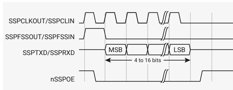
In this mode, SSPCLKOUT and SSPFSSOUT are forced LOW, and the transmit data line, SSPTXD, is tristated whenever the PrimeCell SSP is idle. When the bottom entry of the transmit FIFO contains data, SSPFSSOUT is pulsed HIGH for one SSPCLKOUT period. The value to be transmitted is also transferred from the transmit FIFO to the serial shift register of the transmit logic. On the next rising edge of SSPCLKOUT, the MSB of the 4-bit to 16-bit data frame is shifted out on the SSPTXD pin. In a similar way, the MSB of the received data is shifted onto the SSPRXD pin by the off-chip serial slave device.
Both the PrimeCell SSP and the off-chip serial slave device then clock each data bit into their serial shifter on the falling edge of each SSPCLKOUT. The received data is transferred from the serial shifter to the receive FIFO on the first rising edge of PCLK after the LSB has been latched.
Figure 89 shows the Texas Instruments synchronous serial frame format when back-to-back frames are transmitted.
Figure 89. Texas Instruments synchronous serial frame format, continuous transfer
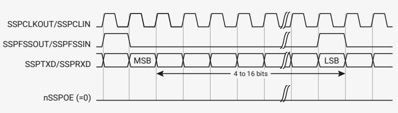
The diagram shows four signals over time: SSPCLKOUT/SSPCLIN, SSPFSSOUT/SSPFSSIN, SSPTXD/SSPRXD, and nSSPOE (=0). The clock signal (SSPCLKOUT/SSPCLIN) is a periodic square wave. The slave select signal (SSPFSSOUT/SSPFSSIN) is a single pulse. The data signal (SSPTXD/SSPRXD) shows a sequence of bits, with the first bit labeled 'MSB' and the last bit labeled 'LSB'. A double arrow indicates a duration of '4 to 16 bits'. The nSSPOE (=0) signal is a constant low level.
4.4.3.9. Motorola SPI frame format
The Motorola SPI interface is a four-wire interface where the SSPFSSOUT signal behaves as a slave select. The main feature of the Motorola SPI format is that you can program the inactive state and phase of the SSPCLKOUT signal using the SPO and SPH bits of the SSPSCR0 control register.
4.4.3.9.1. SPO, clock polarity
When the SPO clock polarity control bit is LOW, it produces a steady state LOW value on the SSPCLKOUT pin. If the SPO clock polarity control bit is HIGH, a steady state HIGH value is placed on the SSPCLKOUT pin when data is not being transferred.
4.4.3.9.2. SPH, clock phase
The SPH control bit selects the clock edge that captures data and enables it to change state. It has the most impact on the first bit transmitted by either permitting or not permitting a clock transition before the first data capture edge.
When the SPH phase control bit is LOW, data is captured on the first clock edge transition.
When the SPH clock phase control bit is HIGH, data is captured on the second clock edge transition.
4.4.3.10. Motorola SPI Format with SPO=0, SPH=0
Figure 90 and Figure 91 shows a continuous transmission signal sequence for Motorola SPI frame format with SPO=0, SPH=0. Figure 90 shows a single transmission signal sequence for Motorola SPI frame format with SPO=0, SPH=0.
Figure 90. Motorola SPI frame format, single transfer, with SPO=0 and SPH=0
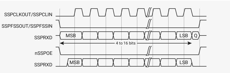
The diagram shows five signals: SSPCLKOUT/SSPCLIN, SSPFSSOUT/SSPFSSIN, SSPRXD, nSSPOE, and SSPTXD. The clock signal (SSPCLKOUT/SSPCLIN) is a periodic square wave. The slave select signal (SSPFSSOUT/SSPFSSIN) is a single pulse. The data signal (SSPRXD) shows a sequence of bits, with the first bit labeled 'MSB' and the last bit labeled 'LSB'. A double arrow indicates a duration of '4 to 16 bits'. The nSSPOE signal is a constant low level. The SSPTXD signal shows a sequence of bits, with the first bit labeled 'MSB' and the last bit labeled 'LSB'. A double arrow indicates a duration of '4 to 16 bits'.
Figure 91 shows a continuous transmission signal sequence for Motorola SPI frame format with SPO=0, SPH=0.
Figure 91. Motorola SPI frame format, single transfer, with SPO=0 and SPH=0
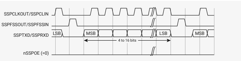
The diagram shows four signals: SSPCLKOUT/SSPCLIN, SSPFSSOUT/SSPFSSIN, SSPTXD/SSPRXD, and nSSPOE (=0). The clock signal (SSPCLKOUT/SSPCLIN) is a periodic square wave. The slave select signal (SSPFSSOUT/SSPFSSIN) is a single pulse. The data signal (SSPTXD/SSPRXD) shows a sequence of bits, with the first bit labeled 'LSB' and the last bit labeled 'MSB'. A double arrow indicates a duration of '4 to 16 bits'. The nSSPOE (=0) signal is a constant low level.
In this configuration, during idle periods:
- the SSPCLKOUT signal is forced LOW
- • the SSPFSSOUT signal is forced HIGH
- • the transmit data line SSPTXD is arbitrarily forced LOW
- • the nSSPOE pad enable signal is forced HIGH (note this is not connected to the pad in RP2040)
- • when the PrimeCell SSP is configured as a master, the nSSPCTL0E line is driven LOW, enabling the SSPCLKOUT pad, active-LOW enable
- • when the PrimeCell SSP is configured as a slave, the nSSPCTL0E line is driven HIGH, disabling the SSPCLKOUT pad, active-LOW enable.
If the PrimeCell SSP is enable, and there is valid data within the transmit FIFO, the start of transmission is signified by the SSPFSSOUT master signal being driven LOW. This causes slave data to be enabled onto the SSPTXD input line of the master. The nSSPOE line is driven LOW, enabling the master SSPTXD output pad.
One-half SSPCLKOUT period later, valid master data is transferred to the SSPTXD pin. Now that both the master and slave data have been set, the SSPCLKOUT master clock pin goes HIGH after one additional half SSPCLKOUT period.
The data is now captured on the rising and propagated on the falling edges of the SSPCLKOUT signal.
In the case of a single word transmission, after all bits of the data word have been transferred, the SSPFSSOUT line is returned to its idle HIGH state one SSPCLKOUT period after the last bit has been captured.
However, in the case of continuous back-to-back transmissions, the SSPFSSOUT signal must be pulsed HIGH between each data word transfer. This is because the slave select pin freezes the data in its serial peripheral register and does not permit it to be altered if the SPH bit is logic zero. Therefore, the master device must raise the SSPFSSIN pin of the slave device between each data transfer to enable the serial peripheral data write. On completion of the continuous transfer, the SSPFSSOUT pin is returned to its idle state one SSPCLKOUT period after the last bit has been captured.
4.4.3.11. Motorola SPI Format with SPO=0, SPH=1
Figure 92 shows the transfer signal sequence for Motorola SPI format with SPO=0, SPH=1, and it covers both single and continuous transfers.
Figure 92. Motorola SPI frame format with SPO=0 and SPH=1, single and continuous transfers
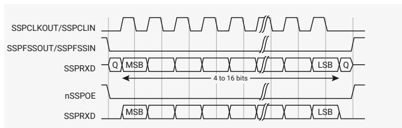
In this configuration, during idle periods:
- • the SSPCLKOUT signal is forced LOW
- • The SSPFSSOUT signal is forced HIGH
- • the transmit data line SSPTXD is arbitrarily forced LOW
- • the nSSPOE pad enable signal is forced HIGH (note this is not connected to the pad in RP2040)
- • when the PrimeCell SSP is configured as a master, the nSSPCTL0E line is driven LOW, enabling the SSPCLKOUT pad, active-LOW enable
- • when the PrimeCell SSP is configured as a slave, the nSSPCTL0E line is driven HIGH, disabling the SSPCLKOUT pad, active-LOW enable.
If the PrimeCell SSP is enabled, and there is valid data within the transmit FIFO, the start of transmission is signified by the SSPFSSOUT master signal being driven LOW. The nSSPOE line is driven LOW, enabling the master SSPTXD output pad. After an additional one half SSPCLKOUT period, both master and slave valid data is enabled onto their respective transmission lines. At the same time, the SSPCLKOUT is enabled with a rising edge transition.
Data is then captured on the falling edges and propagated on the rising edges of the SSPCLKOUT signal.
In the case of a single word transfer, after all bits have been transferred, the SSPFSSOUT line is returned to its idle HIGH state one SSPCLKOUT period after the last bit has been captured. For continuous back-to-back transfers, the SSPFSSOUT pin is held LOW between successive data words and termination is the same as that of the single word transfer.
4.4.3.12. Motorola SPI Format with SPO=1, SPH=0
Figure 93 and Figure 94 show single and continuous transmission signal sequences for Motorola SPI format with SPO=1, SPH=0.
Figure 93 shows a single transmission signal sequence for Motorola SPI format with SPO=1, SPH=0.
Figure 93. Motorola SPI frame format, single transfer, with SPO=1 and SPH=0
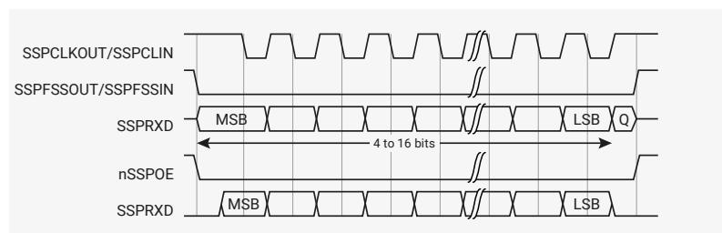
Figure 94 shows a continuous transmission signal sequence for Motorola SPI format with SPO=1, SPH=0.
i NOTE
In Figure 93, Q is an undefined signal.
Figure 94. Motorola SPI frame format, continuous transfer, with SPO=1 and SPH=0
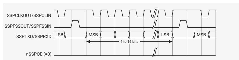
In this configuration, during idle periods:
- • the SSPCLKOUT signal is forced HIGH
- • the SSPFSSOUT signal is forced HIGH
- • the transmit data line SSPTXD is arbitrarily forced LOW
- • the nSSPOE pad enable signal is forced HIGH (note this is not connected to the pad in RP2040)
- • when the PrimeCell SSP is configured as a master, the nSSPCTL0E line is driven LOW, enabling the SSPCLKOUT pad, active-LOW enable
- • when the PrimeCell SSP is configured as a slave, the nSSPCTL0E line is driven HIGH, disabling the SSPCLKOUT pad, active-LOW enable.
If the PrimeCell SSP is enabled, and there is valid data within the transmit FIFO, the start of transmission is signified by the SSPFSSOUT master signal being driven LOW, and this causes slave data to be immediately transferred onto the SSPTXD line of the master. The nSSPOE line is driven LOW, enabling the master SSPTXD output pad.
One half period later, valid master data is transferred to the SSPTXD line. Now that both the master and slave data have been set, the SSPCLKOUT master clock pin becomes LOW after one additional half SSPCLKOUT period. This means that data is captured on the falling edges and be propagated on the rising edges of the SSPCLKOUT signal.
In the case of a single word transmission, after all bits of the data word are transferred, the SSPFSSOUT line is returned to its idle HIGH state one SSPCLKOUT period after the last bit has been captured.
However, in the case of continuous back-to-back transmissions, the SSPFSSOUT signal must be pulsed HIGH between each data word transfer. This is because the slave select pin freezes the data in its serial peripheral register and does not permit it to be altered if the SPH bit is logic zero. Therefore, the master device must raise the SSPFSSIN pin of the slave device between each data transfer to enable the serial peripheral data write. On completion of the continuous transfer, the SSPFSSOUT pin is returned to its idle state one SSPCLKOUT period after the last bit has been captured.
4.4.3.13. Motorola SPI Format with SPO=1, SPH=1
Figure 95 shows the transfer signal sequence for Motorola SPI format with SPO=1, SPH=1, and it covers both single and continuous transfers.
Figure 95. Motorola SPI frame format with SPO=1 and SPH=1, single and continuous transfers
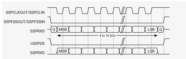
i NOTE
In Figure 95, Q is an undefined signal.
In this configuration, during idle periods:
- • the SSPCLKOUT signal is forced HIGH
- • the SSPFSSOUT signal is forced HIGH
- • the transmit data line SSPTXD is arbitrarily forced LOW
- • the nSSPOE pad enable signal is forced HIGH (note this is not connected to the pad in RP2040)
- • when the PrimeCell SSP is configured as a master, the nSSPCTL0E line is driven LOW, enabling the SSPCLKOUT pad, active-LOW enable
- • when the PrimeCell SSP is configured as a slave, the nSSPCTL0E line is driven HIGH, disabling the SSPCLKOUT pad, active-LOW enable.
If the PrimeCell SSP is enabled, and there is valid data within the transmit FIFO, the start of transmission is signified by the SSPFSSOUT master signal being driven LOW. The nSSPOE line is driven LOW, enabling the master SSPTXD output pad. After an additional one half SSPCLKOUT period, both master and slave data are enabled onto their respective transmission lines. At the same time, the SSPCLKOUT is enabled with a falling edge transition. Data is then captured on the rising edges and propagated on the falling edges of the SSPCLKOUT signal.
After all bits have been transferred, in the case of a single word transmission, the SSPFSSOUT line is returned to its idle HIGH state one SSPCLKOUT period after the last bit has been captured.
For continuous back-to-back transmissions, the SSPFSSOUT pin remains in its active-LOW state, until the final bit of the last word has been captured, and then returns to its idle state as the previous section describes.
For continuous back-to-back transfers, the SSPFSSOUT pin is held LOW between successive data words and termination is the same as that of the single word transfer.
4.4.3.14. National Semiconductor Microwire frame format
Figure 96 shows the National Semiconductor Microwire frame format for a single frame. Figure 97 shows the same format when back to back frames are transmitted.
Figure 96. Microwire frame format, single transfer
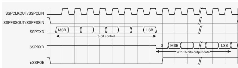
Microwire format is very similar to SPI format, except that transmission is half-duplex instead of full-duplex, using a master-slave message passing technique. Each serial transmission begins with an 8-bit control word that is transmitted from the PrimeCell SSP to the off-chip slave device. During this transmission, the PrimeCell SSP receives no incoming data. After the message has been sent, the off-chip slave decodes it and, after waiting one serial clock after the last bit of the 8-bit control message has been sent, responds with the required data. The returned data is 4 to 16 bits in length, making the total frame length in the range 13-25 bits.
In this configuration, during idle periods:
- • SSPCLKOUT is forced LOW
- • SSPFSSOUT is forced HIGH
- • the transmit data line, SSPTXD, is arbitrarily forced LOW
- • the nSSPOE pad enable signal is forced HIGH (note this is not connected to the pad in RP2040)
A transmission is triggered by writing a control byte to the transmit FIFO. The falling edge of SSPFSSOUT causes the value contained in the bottom entry of the transmit FIFO to be transferred to the serial shift register of the transmit logic, and the MSB of the 8-bit control frame to be shifted out onto the SSPTXD pin. SSPFSSOUT remains LOW for the duration of the frame transmission. The SSPRXD pin remains tristated during this transmission.
The off-chip serial slave device latches each control bit into its serial shifter on the rising edge of each SSPCLKOUT. After the last bit is latched by the slave device, the control byte is decoded during a one clock wait-state, and the slave responds by transmitting data back to the PrimeCell SSP. Each bit is driven onto SSPRXD line on the falling edge of SSPCLKOUT. The PrimeCell SSP in turn latches each bit on the rising edge of SSPCLKOUT. At the end of the frame, for single transfers, the SSPFSSOUT signal is pulled HIGH one clock period after the last bit has been latched in the receive serial shifter, that causes the data to be transferred to the receive FIFO.
NOTE
The off-chip slave device can tristate the receive line either on the falling edge of SSPCLKOUT after the LSB has been latched by the receive shifter, or when the SSPFSSOUT pin goes HIGH.
For continuous transfers, data transmission begins and ends in the same manner as a single transfer. However, the SSPFSSOUT line is continuously asserted, held LOW, and transmission of data occurs back-to-back. The control byte of the next frame follows directly after the LSB of the received data from the current frame. Each of the received values is transferred from the receive shifter on the falling edge SSPCLKOUT, after the LSB of the frame has been latched into the PrimeCell SSP.
Figure 97 shows the National Semiconductor Microwire frame format when back-to-back frames are transmitted.
Figure 97. Microwire frame format, continuous transfers
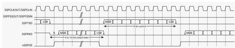
In Microwire mode, the PrimeCell SSP slave samples the first bit of receive data on the rising edge of SSPCLKIN after SSPFSSIN has gone LOW. Masters that drive a free-running SSPCKLIN must ensure that the SSPFSSIN signal has sufficient setup and hold margins with respect to the rising edge of SSPCLKIN.
Figure 98 shows these setup and hold time requirements.
With respect to the SSPCLKIN rising edge on which the first bit of receive data is to be sampled by the PrimeCell SSP slave, SSPFSSIN must have a setup of at least two times the period of SSPCLK on which the PrimeCell SSP operates.
With respect to the SSPCLKIN rising edge previous to this edge, SSPFSSIN must have a hold of at least one SSPCLK period.
Figure 98. Microwire frame format, SSPFSSIN input setup and hold requirements
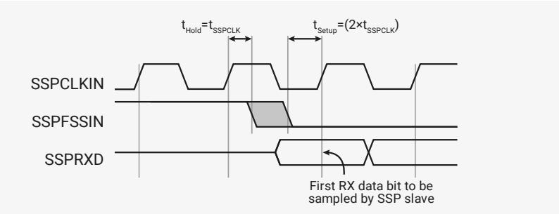
The diagram shows three signals: SSPCLKIN (a periodic square wave), SSPFSSIN (a signal that transitions from high to low), and SSPRXD (a signal that transitions from high to low). The setup time \( t_{Setup} = (2 \times t_{SSPCLK}) \) is the time before the SSPCLKIN rising edge that SSPFSSIN must be stable. The hold time \( t_{Hold} = t_{SSPCLK} \) is the time after the SSPCLKIN rising edge that SSPFSSIN must remain stable. The first RX data bit to be sampled by the SSP slave is indicated by an arrow pointing to the first rising edge of SSPRXD.
4.4.3.15. Examples of master and slave configurations
Figure 99, Figure 100, and Figure 101 shows how you can connect the PrimeCell SSP (PL022) peripheral to other synchronous serial peripherals, when it is configured as a master or a slave.
NOTE
The SSP (PL022) does not support dynamic switching between master and slave in a system. Each instance is configured and connected either as a master or slave.
Figure 99 shows the PrimeCell SSP (PL022) instantiated twice, as a single master and one slave. The master can broadcast to the slave through the master SSPTXD line. In response, the slave drives its nSSPOE signal HIGH, enabling its SSPTXD data onto the SSPRXD line of the master.
Figure 99. PrimeCell SSP master coupled to a PL022 slave
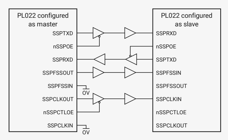
The diagram shows two PL022 blocks. The left block is 'PL022 configured as master' and the right block is 'PL022 configured as slave'. The connections are as follows: Master SSPTXD to Slave SSPRXD; Master nSSPOE to Slave nSSPOE; Master SSPRXD to Slave SSPTXD; Master SSPFSSOUT to Slave SSPFSSIN; Master SSPFSSIN to GND (0V); Master SSPCLKOUT to Slave SSPCLKIN; Master nSSPCTLOE to Slave nSSPCTLOE; Master SSPCLKIN to GND (0V); and Master SSPCLKOUT to Slave SSPCLKOUT.
Figure 100 shows how an PrimeCell SSP (PL022), configured as master, interfaces to a Motorola SPI slave. The SPI Slave Select (SS) signal is permanently tied LOW and configures it as a slave. Similar to the above operation, the master can broadcast to the slave through the master PrimeCell SSP SSPTXD line. In response, the slave drives its SPI MISO port onto the SSPRXD line of the master.
Figure 100. PrimeCell SSP master coupled to an SPI slave
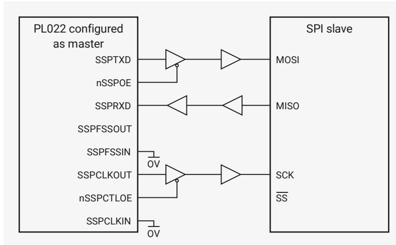
Figure 101 shows a Motorola SPI configured as a master and interfaced to an instance of a PrimeCell SSP (PL022) configured as a slave. In this case, the slave Select Signal (SS) is permanently tied HIGH to configure it as a master. The master can broadcast to the slave through the master SPI MOSI line and in response, the slave drives its nSSPOE signal LOW. This enables its SSPTXD data onto the MISO line of the master.
Figure 101. SPI master coupled to a PrimeCell SSP slave
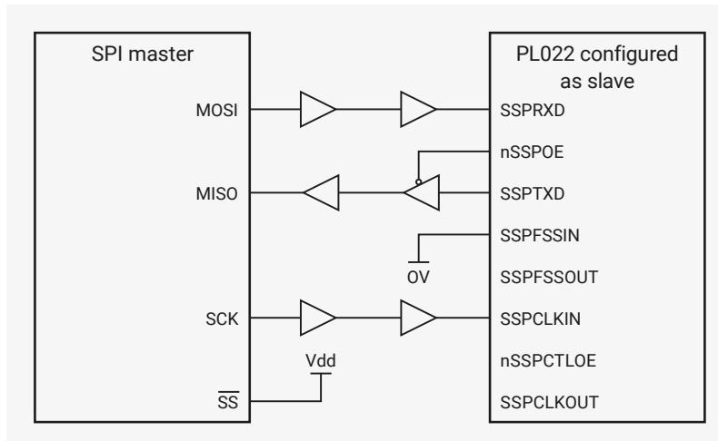
4.4.3.16. PrimeCell DMA interface
The PrimeCell SSP provides an interface to connect to the DMA controller. The PrimeCell SSP DMA control register, SSPDMACR controls the DMA operation of the PrimeCell SSP.
The DMA interface includes the following signals, for receive:
SSPRXDMSREQ
Single-character DMA transfer request, asserted by the SSP. This signal is asserted when the receive FIFO contains at least one character.
SSPRXDMABREQ
Burst DMA transfer request, asserted by the SSP. This signal is asserted when the receive FIFO contains four or more characters.
SSPRXDMACLR
DMA request clear, asserted by the DMA controller to clear the receive request signals. If DMA burst transfer is requested, the clear signal is asserted during the transfer of the last data in the burst.
The DMA interface includes the following signals, for transmit:
SSPTXDMASREQ
Single-character DMA transfer request, asserted by the SSP. This signal is asserted when there is at least one empty location in the transmit FIFO.
SSPTXDMABREQ
Burst DMA transfer request, asserted by the SSP. This signal is asserted when the transmit FIFO contains four characters or fewer.
SSPTXDMACLR
DMA request clear, asserted by the DMA controller, to clear the transmit request signals. If a DMA burst transfer is requested, the clear signal is asserted during the transfer of the last data in the burst.
The burst transfer and single transfer request signals are not mutually exclusive. They can both be asserted at the same time. For example, when there is more data than the watermark level of four in the receive FIFO, the burst transfer request, and the single transfer request, are asserted. When the amount of data left in the receive FIFO is less than the watermark level, the single request only is asserted. This is useful for situations where the number of characters left to be received in the stream is less than a burst.
For example, if 19 characters must be received, the DMA controller then transfers four bursts of four characters, and three single transfers to complete the stream.
NOTE
For the remaining three characters, the PrimeCell SSP does not assert the burst request.
Each request signal remains asserted until the relevant DMA clear signal is asserted. After the request clear signal is deasserted, a request signal can become active again, depending on the conditions that previous sections describe. All request signals are deasserted if the PrimeCell SSP is disabled, or the DMA enable signal is cleared.
Table 495 shows the trigger points for DMABREQ, for both the transmit and receive FIFOs.
Table 495. DMA trigger points for the transmit and receive FIFOs
| Burst length | ||
|---|---|---|
| Watermark level | Transmit, number of empty locations | Receive, number of filled locations |
| 1/2 | 4 | 4 |
Figure 102 shows the timing diagram for both a single transfer request, and a burst transfer request, with the appropriate DMA clear signal. The signals are all synchronous to PCLK.
Figure 102. DMA transfer waveforms

The diagram shows four digital signals over time, synchronized to a PCLK clock. PCLK is a periodic square wave. DMASREQ (single transfer request) is asserted at PCLK cycles 1, 2, 3, and 4, then deasserted at cycle 5. DMABREQ (burst transfer request) is asserted at PCLK cycles 1, 2, 3, and 4, then deasserted at cycle 5. DMACLR (DMA request clear) is asserted at PCLK cycle 5 and remains asserted until cycle 10, after which it is deasserted. The signals are all synchronous to the PCLK clock.
4.4.4. List of Registers
The SPI0 and SPI1 registers start at base addresses of 0x4003c000 and 0x40040000 respectively (defined as SPI0_BASE and SPI1_BASE in SDK).
Table 496. List of SPI registers
| Offset | Name | Info |
|---|---|---|
| 0x000 | SSPCR0 | Control register 0, SSPCR0 on page 3-4 |
| 0x004 | SSPCR1 | Control register 1, SSPCR1 on page 3-5 |
| 0x008 | SSPDR | Data register, SSPDR on page 3-6 |
| 0x00c | SSPSR | Status register, SSPSR on page 3-7 |
| 0x010 | SSPCPSR | Clock prescale register, SSPCPSR on page 3-8 |
| Offset | Name | Info |
|---|---|---|
| 0x014 | SSPIMSC | Interrupt mask set or clear register, SSPIMSC on page 3-9 |
| 0x018 | SSPRIS | Raw interrupt status register, SSPRIS on page 3-10 |
| 0x01c | SSPMIS | Masked interrupt status register, SSPMIS on page 3-11 |
| 0x020 | SSPICR | Interrupt clear register, SSPICR on page 3-11 |
| 0x024 | SSPDMACR | DMA control register, SSPDMACR on page 3-12 |
| 0xfe0 | SSPPERIPHID0 | Peripheral identification registers, SSPPeriphID0-3 on page 3-13 |
| 0xfe4 | SSPPERIPHID1 | Peripheral identification registers, SSPPeriphID0-3 on page 3-13 |
| 0xfe8 | SSPPERIPHID2 | Peripheral identification registers, SSPPeriphID0-3 on page 3-13 |
| 0xfec | SSPPERIPHID3 | Peripheral identification registers, SSPPeriphID0-3 on page 3-13 |
| 0xff0 | SSPPCELLID0 | PrimeCell identification registers, SSPPCellID0-3 on page 3-16 |
| 0xff4 | SSPPCELLID1 | PrimeCell identification registers, SSPPCellID0-3 on page 3-16 |
| 0xff8 | SSPPCELLID2 | PrimeCell identification registers, SSPPCellID0-3 on page 3-16 |
| 0xffc | SSPPCELLID3 | PrimeCell identification registers, SSPPCellID0-3 on page 3-16 |
SPI: SSPCR0 Register
Offset: 0x000
Description
Control register 0, SSPCR0 on page 3-4
Table 497. SSPCR0 Register
| Bits | Description | Type | Reset |
|---|---|---|---|
| 31:16 | Reserved. | - | - |
| 15:8 | SCR : Serial clock rate. The value SCR is used to generate the transmit and receive bit rate of the PrimeCell SSP. The bit rate is: \( F_{SSPCLK} \times \text{CPSDVSR} \times (1 + \text{SCR}) \) where CPSDVSR is an even value from 2-254, programmed through the SSPCPSR register and SCR is a value from 0-255. | RW | 0x00 |
| 7 | SPH : SSPCLKOUT phase, applicable to Motorola SPI frame format only. See Motorola SPI frame format on page 2-10. | RW | 0x0 |
| 6 | SPO : SSPCLKOUT polarity, applicable to Motorola SPI frame format only. See Motorola SPI frame format on page 2-10. | RW | 0x0 |
| 5:4 | FRF : Frame format: 00 Motorola SPI frame format. 01 TI synchronous serial frame format. 10 National Microwire frame format. 11 Reserved, undefined operation. | RW | 0x0 |
| 3:0 | DSS : Data Size Select: 0000 Reserved, undefined operation. 0001 Reserved, undefined operation. 0010 Reserved, undefined operation. 0011 4-bit data. 0100 5-bit data. 0101 6-bit data. 0110 7-bit data. 0111 8-bit data. 1000 9-bit data. 1001 10-bit data. 1010 11-bit data. 1011 12-bit data. 1100 13-bit data. 1101 14-bit data. 1110 15-bit data. 1111 16-bit data. | RW | 0x0 |
SPI: SSPCR1 Register
Offset: 0x004
Description
Control register 1, SSPCR1 on page 3-5
Table 498. SSPCR1 Register
| Bits Register 31:0 Bits | column_2 | Description Description | Type RO Type | Reset 0x00000001 Reset |
|---|---|---|---|---|
| 31:4 | Reserved. | - | - | |
| 3 | SOD | : Slave-mode output disable. This bit is relevant only in the slave mode, slave drives data onto its serial output line. In such systems the RXD lines | RW | 0x0 |
| 2 | MS | not drive the SSPTXD output in slave mode. : Master or slave mode select. This bit can be modified only when the Device configured as slave. | RW | 0x0 |
| 1 | SSE | : Synchronous serial port enable: 0 SSP operation disabled. 1 SSP operation enabled. | RW | 0x0 |
| 0 | LBM | : Loop back mode: 0 Normal serial port operation enabled. 1 Output of | RW | 0x0 |
| Bits | Description | Type | Reset | |
| 31:16 | Reserved. | - | - | |
| 15:0 | DATA | : Transmit/Receive FIFO: Read Receive FIFO. Write Transmit FIFO. You The receive logic automatically right-justifies. | RWF | - |
| Bits | Description | Type | Reset | |
| 31:5 | Reserved. | - | - | |
| 4 | BSY | : PrimeCell SSP busy flag, RO: 0 SSP is idle. 1 SSP is currently transmitting and/or receiving a frame or the transmit FIFO is not empty. | RO | 0x0 |
| 3 | RFF | : Receive FIFO full, RO: 0 Receive FIFO is not full. 1 Receive FIFO is full. | RO | 0x0 |
| 2 | RNE | : Receive FIFO not empty, RO: 0 Receive FIFO is empty. 1 Receive FIFO is not empty. | RO | 0x0 |
| 1 | TNF full. | : Transmit FIFO not full, RO: 0 Transmit FIFO is full. 1 Transmit FIFO is not | RO | 0x1 |
| 0 | TFE | : Transmit FIFO empty, RO: 0 Transmit FIFO is not empty. 1 Transmit FIFO is empty. | RO | 0x1 |
SPI: SSPDR Register
Offset: 0x008
Description
Data register, SSPDR on page 3-6
Table 499. SSPDR Register
SPI: SSPSR Register
Offset: 0x00c
Description
Status register, SSPSR on page 3-7
Table 500. SSPSR Register
SPI: SSPCPSR Register
Offset: 0x010
Description
Clock prescale register, SSPCPSR on page 3-8
Table 501. SSPCPSR Register
| Bits | Description | Type | Reset |
|---|---|---|---|
| 31:8 | Reserved. | - | - |
| 7:0 | CPSDVSR : Clock prescale divisor. Must be an even number from 2-254, depending on the frequency of SSPCLK. The least significant bit always returns zero on reads. | RW | 0x00 |
SPI: SSPIMSC Register
Offset: 0x014
Description
Interrupt mask set or clear register, SSPIMSC on page 3-9
Table 502. SSPIMSC Register
| Bits | Description | Type | Reset |
|---|---|---|---|
| 31:4 | Reserved. | - | - |
| 3 | TXIM : Transmit FIFO interrupt mask: 0 Transmit FIFO half empty or less condition interrupt is masked. 1 Transmit FIFO half empty or less condition interrupt is not masked. | RW | 0x0 |
| 2 | RXIM : Receive FIFO interrupt mask: 0 Receive FIFO half full or less condition interrupt is masked. 1 Receive FIFO half full or less condition interrupt is not masked. | RW | 0x0 |
| 1 | RTIM : Receive timeout interrupt mask: 0 Receive FIFO not empty and no read prior to timeout period interrupt is masked. 1 Receive FIFO not empty and no read prior to timeout period interrupt is not masked. | RW | 0x0 |
| 0 | RORIM : Receive overrun interrupt mask: 0 Receive FIFO written to while full condition interrupt is masked. 1 Receive FIFO written to while full condition interrupt is not masked. | RW | 0x0 |
SPI: SSPRIS Register
Offset: 0x018
Description
Raw interrupt status register, SSPRIS on page 3-10
Table 503. SSPRIS Register
| Bits | Description | Type | Reset |
|---|---|---|---|
| 31:4 | Reserved. | - | - |
| 3 | TXRIS : Gives the raw interrupt state, prior to masking, of the SSPTXINTR interrupt | RO | 0x1 |
| 2 | RXRIS : Gives the raw interrupt state, prior to masking, of the SSPRXINTR interrupt | RO | 0x0 |
| 1 | RTRIS : Gives the raw interrupt state, prior to masking, of the SSPRTINTR interrupt | RO | 0x0 |
| Bits | Description | Type | Reset |
|---|---|---|---|
| 0 | RORRIS : Gives the raw interrupt state, prior to masking, of the SSPRORINTR interrupt | RO | 0x0 |
SPI: SSPMIS Register
Offset: 0x01c
Description
Masked interrupt status register, SSPMIS on page 3-11
Table 504. SSPMIS Register
| Bits | Description | Type | Reset |
|---|---|---|---|
| 31:4 | Reserved. | - | - |
| 3 | TXMIS : Gives the transmit FIFO masked interrupt state, after masking, of the SSPTXINTR interrupt | RO | 0x0 |
| 2 | RXMIS : Gives the receive FIFO masked interrupt state, after masking, of the SSPRXINTR interrupt | RO | 0x0 |
| 1 | RTMIS : Gives the receive timeout masked interrupt state, after masking, of the SSPRTINTR interrupt | RO | 0x0 |
| 0 | RORMIS : Gives the receive over run masked interrupt status, after masking, of the SSPRORINTR interrupt | RO | 0x0 |
SPI: SSPICR Register
Offset: 0x020
Description
Interrupt clear register, SSPICR on page 3-11
Table 505. SSPICR Register
| Bits | Description | Type | Reset |
|---|---|---|---|
| 31:2 | Reserved. | - | - |
| 1 | RTIC : Clears the SSPRTINTR interrupt | WC | 0x0 |
| 0 | RORIC : Clears the SSPRORINTR interrupt | WC | 0x0 |
SPI: SSPDMACR Register
Offset: 0x024
Description
DMA control register, SSPDMACR on page 3-12
Table 506. SSPDMACR Register
| Bits | Description | Type | Reset |
|---|---|---|---|
| 31:2 | Reserved. | - | - |
| 1 | TXDMAE : Transmit DMA Enable. If this bit is set to 1, DMA for the transmit FIFO is enabled. | RW | 0x0 |
| 0 | RXDMAE : Receive DMA Enable. If this bit is set to 1, DMA for the receive FIFO is enabled. | RW | 0x0 |
SPI: SSPPERIPHID0 Register
Offset: 0xfe0
Description
Peripheral identification registers, SSPPeriphID0-3 on page 3-13
Table 507.
SSPPERIPHID0
Register
| Bits | Description | Type | Reset |
|---|---|---|---|
| 31:8 | Reserved. | - | - |
| 7:0 | PARTNUMBER0 : These bits read back as 0x22 | RO | 0x22 |
SPI: SSPPERIPHID1 Register
Offset: 0xfe4
Description
Peripheral identification registers, SSPPeriphID0-3 on page 3-13
Table 508.
SSPPERIPHID1
Register
| Bits | Description | Type | Reset |
|---|---|---|---|
| 31:8 | Reserved. | - | - |
| 7:4 | DESIGNER0 : These bits read back as 0x1 | RO | 0x1 |
| 3:0 | PARTNUMBER1 : These bits read back as 0x0 | RO | 0x0 |
SPI: SSPPERIPHID2 Register
Offset: 0xfe8
Description
Peripheral identification registers, SSPPeriphID0-3 on page 3-13
Table 509.
SSPPERIPHID2
Register
| Bits | Description | Type | Reset |
|---|---|---|---|
| 31:8 | Reserved. | - | - |
| 7:4 | REVISION : These bits return the peripheral revision | RO | 0x3 |
| 3:0 | DESIGNER1 : These bits read back as 0x4 | RO | 0x4 |
SPI: SSPPERIPHID3 Register
Offset: 0xfec
Description
Peripheral identification registers, SSPPeriphID0-3 on page 3-13
Table 510.
SSPPERIPHID3
Register
| Bits | Description | Type | Reset |
|---|---|---|---|
| 31:8 | Reserved. | - | - |
| 7:0 | CONFIGURATION : These bits read back as 0x00 | RO | 0x00 |
SPI: SSPPCELLID0 Register
Offset: 0xff0
Description
PrimeCell identification registers, SSPPCellID0-3 on page 3-16
Table 511.
SSPPCELLID0 Register
| Bits | Description | Type | Reset |
|---|---|---|---|
| 31:8 | Reserved. | - | - |
| 7:0 | SSPPCELLID0 : These bits read back as 0x0D | RO | 0x0d |
SPI: SSPPCELLID1 Register
Offset: 0xff4
Description
PrimeCell identification registers, SSPPCellIID0-3 on page 3-16
Table 512.
SSPPCELLID1 Register
| Bits | Description | Type | Reset |
|---|---|---|---|
| 31:8 | Reserved. | - | - |
| 7:0 | SSPPCELLID1 : These bits read back as 0xF0 | RO | 0xf0 |
SPI: SSPPCELLID2 Register
Offset: 0xff8
Description
PrimeCell identification registers, SSPPCellIID0-3 on page 3-16
Table 513.
SSPPCELLID2 Register
| Bits | Description | Type | Reset |
|---|---|---|---|
| 31:8 | Reserved. | - | - |
| 7:0 | SSPPCELLID2 : These bits read back as 0x05 | RO | 0x05 |
SPI: SSPPCELLID3 Register
Offset: 0xffc
Description
PrimeCell identification registers, SSPPCellIID0-3 on page 3-16
Table 514.
SSPPCELLID3 Register
| Bits | Description | Type | Reset |
|---|---|---|---|
| 31:8 | Reserved. | - | - |
| 7:0 | SSPPCELLID3 : These bits read back as 0xB1 | RO | 0xb1 |
4.5. PWM
4.5.1. Overview
Pulse width modulation (PWM) is a scheme where a digital signal provides a smoothly varying average voltage. This is achieved with positive pulses of some controlled width, at regular intervals. The fraction of time spent high is known as the duty cycle. This may be used to approximate an analog output, or control switchmode power electronics.
The RP2040 PWM block has 8 identical slices. Each slice can drive two PWM output signals, or measure the frequency or duty cycle of an input signal. This gives a total of up to 16 controllable PWM outputs. All 30 GPIO pins can be driven by the PWM block.
Figure 103. A single PWM slice. A 16-bit counter counts from 0 up to some programmed value, and then wraps to zero, or counts back down again, depending on PWM mode. The A and B outputs transition high and low based on the current count value and the preprogrammed A and B thresholds. The counter advances based on a number of events: it may be free-running, or gated by level or edge of an input signal on the B pin. A fractional divider slows the overall count rate for finer control of output frequency.
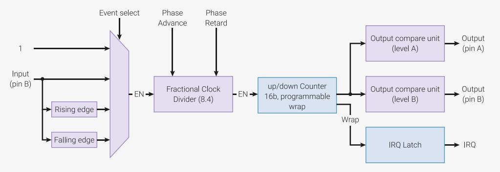
Each PWM slice is equipped with the following:
- • 16-bit counter
- • 8.4 fractional clock divider
- • Two independent output channels, duty cycle from 0% to 100% inclusive
- • Dual slope and trailing edge modulation
- • Edge-sensitive input mode for frequency measurement
- • Level-sensitive input mode for duty cycle measurement
- • Configurable counter wrap value
- ◦ Wrap and level registers are double buffered and can be changed race-free while PWM is running
- • Interrupt request and DMA request on counter wrap
- • Phase can be precisely advanced or retarded while running (increments of one count)
Slices can be enabled or disabled simultaneously via a single, global control register. The slices then run in perfect lockstep, so that more complex power circuitry can be switched by the outputs of multiple slices.
4.5.2. Programmer’s Model
All 30 GPIO pins on RP2040 can be used for PWM:
Table 515. Mapping of PWM channels to GPIO pins on RP2040. This is also shown in the main GPIO function table, Table 279
| GPIO | 0 | 1 | 2 | 3 | 4 | 5 | 6 | 7 | 8 | 9 | 10 | 11 | 12 | 13 | 14 | 15 |
| PWM Channel | 0A | 0B | 1A | 1B | 2A | 2B | 3A | 3B | 4A | 4B | 5A | 5B | 6A | 6B | 7A | 7B |
| GPIO | 16 | 17 | 18 | 19 | 20 | 21 | 22 | 23 | 24 | 25 | 26 | 27 | 28 | 29 | ||
| PWM Channel | 0A | 0B | 1A | 1B | 2A | 2B | 3A | 3B | 4A | 4B | 5A | 5B | 6A | 6B |
- • The 16 PWM channels (8 2-channel slices) appear on GPIO0 to GPIO15, in the order PWM0 A, PWM0 B, PWM1 A...
- • This repeats for GPIO16 to GPIO29. GPIO16 is PWM0 A, GPIO17 is PWM0 B, so on up to PWM6 B on GPIO29
- • The same PWM output can be selected on two GPIO pins; the same signal will appear on each GPIO.
- • If a PWM B pin is used as an input, and is selected on multiple GPIO pins, then the PWM slice will see the logical OR of those two GPIO inputs
4.5.2.1. Pulse Width Modulation
The PWM hardware functions by continuously comparing the input value to a free-running counter. This produces a toggling output where the amount of time spent at the high output level is proportional to the input value. The fraction of time spent at the high signal level is known as the duty cycle of the signal.
The counting period is controlled by the TOP register, with a maximum possible period of 65536 cycles, as the counter and TOP are 16 bits in size. The input values are configured via the CC register.
Figure 104. The counter repeatedly counts from 0 to TOP , forming a sawtooth shape. The counter is continuously compared with some input value. When the input value is higher than the counter, the output is driven high. Otherwise, the output is low. The output period \( T \) is defined by the TOP value of the counter, and how fast the counter is configured to count. The average output voltage, as a fraction of the IO power supply, is the input value divided by the counter period ( \( \text{TOP} + 1 \) )
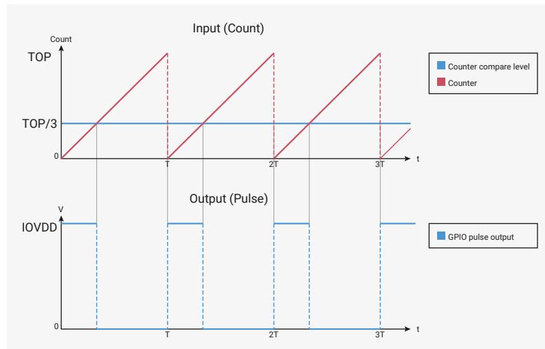
This example shows the counting period and the A and B counter compare levels being configured on one of RP2040's PWM slices.
Pico Examples: https://github.com/raspberrypi/pico-examples/blob/master/pwm/hello_pwm/hello_pwm.c Lines 14 - 29
14 // Tell GPIO 0 and 1 they are allocated to the PWM
15 gpio_set_function(0, GPIO_FUNC_PWM);
16 gpio_set_function(1, GPIO_FUNC_PWM);
17
18 // Find out which PWM slice is connected to GPIO 0 (it's slice 0)
19 uint slice_num = pwm_gpio_to_slice_num(0);
20
21 // Set period of 4 cycles (0 to 3 inclusive)
22 pwm_set_wrap(slice_num, 3);
23 // Set channel A output high for one cycle before dropping
24 pwm_set_chan_level(slice_num, PWM_CHAN_A, 1);
25 // Set initial B output high for three cycles before dropping
26 pwm_set_chan_level(slice_num, PWM_CHAN_B, 3);
27 // Set the PWM running
28 pwm_set_enabled(slice_num, true);
Figure 105 shows how the PWM hardware operates once it has been configured in this way.
Figure 105. The slice counts repeatedly from 0 to 3, which is configured as the TOP value. The output waves therefore have a period of 4. Output A is high for 1 cycle in 4, so the average output voltage is 1/4 of the IO supply voltage. Output B is high for 3 cycles in every 4. Note the rising edges of A and B are always aligned.

The default behaviour of a PWM slice is to count upward until the value of the TOP register is reached, and then immediately wrap to 0. PWM slices also offer a phase-correct mode, enabled by setting CSR_PH_CORRECT to 1, where the counter starts to count downward after reaching TOP, until it reaches 0 again.
It is called phase-correct mode because the pulse is always centred on the same point, no matter the duty cycle. In other words, its phase is not a function of duty cycle. The output frequency is halved when phase-correct mode is enabled.
Figure 106. In phase-correct mode, the counter counts back down from TOP to 0 once it reaches TOP.
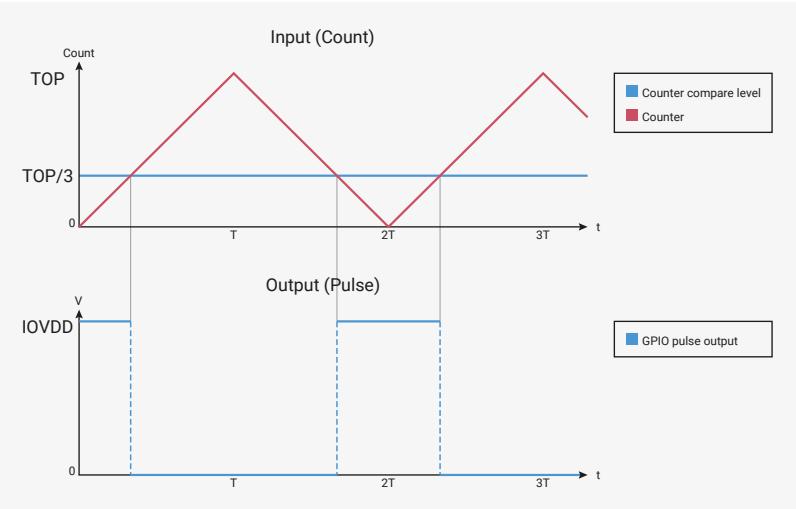
4.5.2.2. 0% and 100% Duty Cycle
The RP2040 PWM can produce toggle-free 0% and 100% duty cycle output.
Figure 107. Glitch-free 0% duty cycle output for CC = 0, and glitch-free 100% duty cycle output for CC = TOP + 1
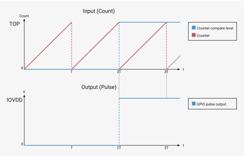
A CC value of 0 will produce a 0% output, i.e. the output signal is always low. A CC value of TOP + 1 (i.e. equal to the period, in non-phase-correct mode) will produce a 100% output. For example, if TOP is programmed to 254, the counter will have a period of 255 cycles, and CC values in the range of 0 to 255 inclusive will produce duty cycles in the range 0% to 100% inclusive.
Glitch-free output at 0% and 100% is important e.g. to avoid switching losses when a MOSFET is controlled at its minimum and maximum current levels.
4.5.2.3. Double Buffering
Figure 108 shows how a change in input value will produce a change in output duty cycle. This can be used to approximate some analog waveform such as a sine wave.
Figure 108. The input value varies with each counter period: first \( TOP/3 \) , then \( 2 \times TOP/3 \) , and finally \( TOP + 1 \) for 100% duty cycle. Each increase in the input value causes a corresponding increase in the output duty cycle.
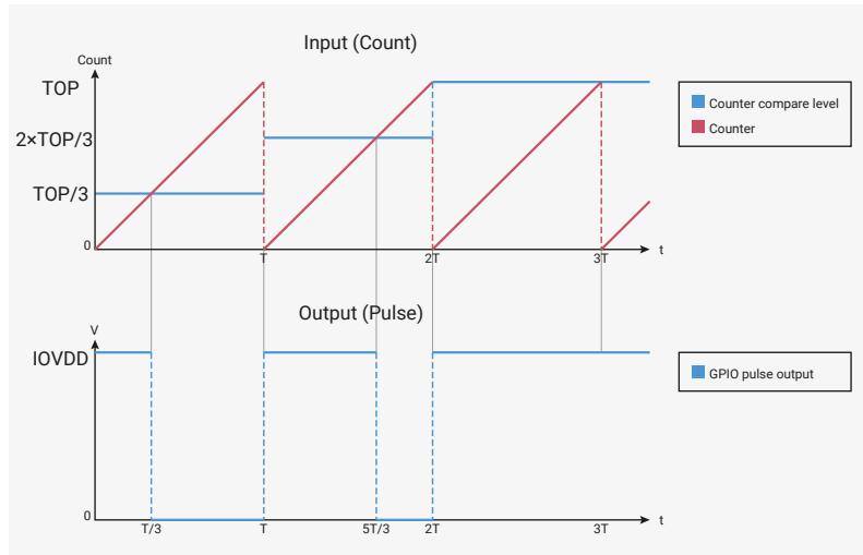
The figure consists of two vertically aligned graphs sharing a common time axis
\(
t
\)
.
The top graph, titled 'Input (Count)', has a vertical axis labeled 'Count'. It shows a red line representing the counter, which increases linearly from 0 to
\(
TOP
\)
and then resets to 0 at times
\(
t
\)
,
\(
2T
\)
, and
\(
3T
\)
. A blue step function represents the 'Counter compare level'. It starts at
\(
TOP/3
\)
from
\(
t=0
\)
to
\(
t=T
\)
, jumps to
\(
2 \times TOP/3
\)
at
\(
t=T
\)
, and jumps to
\(
TOP
\)
at
\(
t=2T
\)
.
The bottom graph, titled 'Output (Pulse)', has a vertical axis labeled
\(
V
\)
. It shows the 'GPIO pulse output' as a blue square wave. The output is high (at level
\(
IOVDD
\)
) when the counter value is less than the current compare level, and low (at 0) otherwise. The duty cycle of the output increases as the compare level increases.
In Figure 108, the input value only changes at the instant where the counter wraps through 0. Figure 109 shows what happens if the input value is allowed to change at any other time: an unwanted glitch is produced at the output.
Figure 109. The input value changes whilst the counter is mid-ramp. This produces additional toggling at the output.
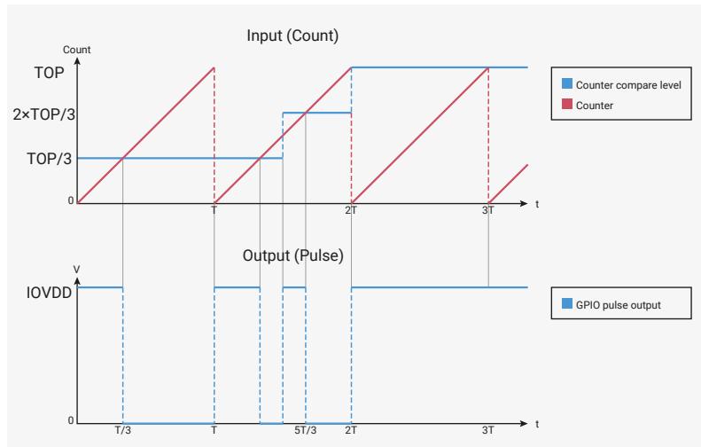
This figure is similar to Figure 108 but illustrates a glitch scenario. The counter (red) and its wraps at \( t \) , \( 2T \) , and \( 3T \) are the same. However, the compare level (blue) starts at \( TOP/3 \) until \( t=T \) , then jumps to \( 2 \times TOP/3 \) at \( t=T \) . At a later time, \( 5T/3 \) , the compare level jumps again to \( TOP \) while the counter is still in its mid-ramp. This second jump causes an additional transition in the output pulse (blue) at \( 5T/3 \) , which is an unwanted glitch.
The behaviour becomes even more perplexing if the \( TOP \) register is also modified. It would be difficult for software to write to \( CC \) or \( TOP \) with the correct timing. To solve this, each slice has two copies of the \( CC \) and \( TOP \) registers: one copy which software can modify, and another, internal copy which is updated from the first register at the instant the counter wraps. Software can modify its copy of the register at will, but the changes are not captured by the PWM output until the next wrap.
Figure 110 shows the sequence of events where a software interrupt handler changes the value of \( CC\_A \) each time the counter wraps.
Figure 110. Each counter wrap causes the interrupt request signal to assert. The processor enters its interrupt handler, writes to its copy of the CC register, and clears the interrupt. When the counter wraps again, the latched version of the CC register is instantaneously updated with the most recent value written by software, and this value controls the duty cycle for the next period. The IRQ is reasserted so that software can write another fresh value to its copy of the CC register.
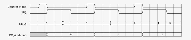
The diagram shows four digital signals over time. The 'Counter at top' signal is a periodic square wave that wraps from a high value to 0. The 'IRQ' signal is a narrow pulse that asserts (goes high) at each counter wrap. The 'CC_A' signal is a periodic square wave that changes value at each counter wrap, with values 0, 1, 2, and 3 shown. The 'CC_A latched' signal is a square wave that is updated to the current value of CC_A at each counter wrap, indicated by a shaded region during the wrap event.
There is no limitation on what values can be written to CC or TOP , or when they are written. In normal PWM mode ( CSR_PH_CORRECT is 0) the latched copies are updated when the counter wraps to 0, which occurs once every TOP + 1 cycles. In phase-correct mode ( CSR_PH_CORRECT is 1), the latched copies are updated on the 0 to 0 count transition, i.e. the point where the counter stops counting downward and begins to count upward again.
4.5.2.4. Clock Divider
Each slice has a fractional clock divider, configured by the DIV register. This is an 8 integer bit, 4 fractional bit clock divider, which allows the count rate to be slowed by up to a factor of 256. The clock divider allows much lower output frequencies to be achieved – approximately 7.5Hz from a 125MHz system clock. Lower frequencies than this will require a system timer interrupt (Section 4.6)
It does this by generating an enable signal which gates the operation of the counter.
Figure 111. The clock divider generates an enable signal. The counter only counts on cycles where this signal is high. A clock divisor of 1 causes the enable to be asserted on every cycle, so the counter counts by one on every system clock cycle. Higher divisors cause the count enable to be asserted less frequently. Fractional division achieves an average fractional counting rate by spacing some enable pulses further apart than others.
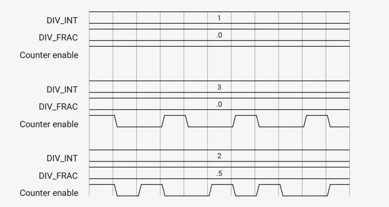
The diagram shows three sets of signals for different clock divisors. Each set includes
DIV_INT
,
DIV_FRAC
, and
Counter enable
signals.
- For divisor 1:
DIV_INT
is 1,
DIV_FRAC
is .0, and
Counter enable
is a continuous high signal.
- For divisor 3:
DIV_INT
is 3,
DIV_FRAC
is .0, and
Counter enable
is a square wave that is high for 1 out of every 3 clock cycles.
- For divisor 2 with a fractional part:
DIV_INT
is 2,
DIV_FRAC
is .5, and
Counter enable
is a square wave that is high for 1.5 out of every 2 clock cycles, achieved by having some high pulses be wider than others.
The fractional divider is a first-order delta-sigma type.
The clock divider also allows the effective count range to be extended, when using level-sensitive or edge-sensitive modes to take duty cycle or frequency measurements.
4.5.2.5. Level-sensitive and Edge-sensitive Triggering
Figure 112. PWM slice event selection. The counter advances when its enable input is high, and this enable is generated in two sequential stages. First, any one of four event types (always on, pin B high, pin B rise, pin B fall) can generate enable pulses for the fractional clock divider. The divider can reduce the rate of the enable pulses, before passing them on to the counter.
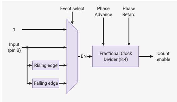
graph LR
    EventSelect[Event select]
    InputB[Input (pin B)]
    RisingEdge[Rising edge]
    FallingEdge[Falling edge]
    EN[EN]
    Divider[Fractional Clock Divider (8.4)]
    PhaseAdvance[Phase Advance]
    PhaseRetard[Phase Retard]
    CountEnable[Count enable]

    EventSelect --> EN
    InputB --> EventSelect
    RisingEdge --> EventSelect
    FallingEdge --> EventSelect
    EN --> Divider
    PhaseAdvance --> Divider
    PhaseRetard --> Divider
    Divider --> CountEnable
By default, each slice's counter is free-running, and will count continuously whenever the slice is enabled. There are three other options available:
- • Count continuously when a high level is detected on the B pin
- • Count once with each rising edge detected on the B pin
- • Count once with each falling edge detected on the B pin
These modes are selected by the
DIVMODE
field in each slice's
CSR
. In free-running mode, the A and B pins are both outputs. In any other mode, the B pin becomes an input, and controls the operation of the counter.
CC_B
is ignored when not in free-running mode.
By allowing the slice to run for a fixed amount of time in level-sensitive or edge-sensitive mode, it's possible to measure the duty cycle or frequency of an input signal. Due to the type of edge-detect circuit used, the low period and high period of the measured signal must both be strictly greater than the system clock period when taking frequency measurements.
The clock divider is still operational in level-sensitive and edge-sensitive mode. At maximum division (writing 0 to
DIV_INT
), the counter will only advance once per 256 high input cycles in level-sensitive modes, or once per 256 edges in edge-sensitive mode. This allows longer-running measurements to be taken, although the resolution is still just 16 bits.
Pico Examples: https://github.com/raspberrypi/pico-examples/blob/master/pwm/measure_duty_cycle/measure_duty_cycle.c Lines 19 - 37
19 float measure_duty_cycle(uint gpio) {
20     // Only the PWM B pins can be used as inputs.
21     assert(pwm_gpio_to_channel(gpio) == PWM_CHAN_B);
22     uint slice_num = pwm_gpio_to_slice_num(gpio);
23
24     // Count once for every 100 cycles the PWM B input is high
25     pwm_config cfg = pwm_get_default_config();
26     pwm_config_set_clkdiv_mode(&cfg, PWM_DIV_B_HIGH);
27     pwm_config_set_clkdiv(&cfg, 100);
28     pwm_init(slice_num, &cfg, false);
29     gpio_set_function(gpio, GPIO_FUNC_PWM);
30
31     pwm_set_enabled(slice_num, true);
32     sleep_ms(10);
33     pwm_set_enabled(slice_num, false);
34     float counting_rate = clock_get_hz(clk_sys) / 100;
35     float max_possible_count = counting_rate * 0.01;
36     return pwm_get_counter(slice_num) / max_possible_count;
37 }
4.5.2.6. Configuring PWM Period
When free-running, the period of a PWM slice's output (measured in system clock cycles) is controlled by three parameters:
- • The TOP register
- • Whether phase-correct mode is enabled ( CSR_PH_CORRECT )
- • The DIV register
The slice counts from 0 to TOP , and then either wraps, or begins counting backward, depending on the setting of CSR_PH_CORRECT . The rate of counting is slowed by the clock divider, with a maximum speed of one count per cycle, and a
minimum speed of one count per \( 255\frac{15}{16} \) cycles. The period in clock cycles can be calculated as:
The output frequency can then be determined based on the system clock frequency:
4.5.2.7. Interrupt Request (IRQ) and DMA Data Request (DREQ)
The PWM block has a single IRQ output. The interrupt status registers INTR , INTS and INTE allow software to control which slices will assert this IRQ output, to check which slices are the cause of the IRQ's assertion, and to clear and acknowledge the interrupt.
A slice generates an interrupt request each time its counter wraps (or, if CSR_PH_CORRECT is enabled, each time the counter returns to 0). This sets the flag corresponding to this slice in the raw interrupt status register, INTR . If this slice's interrupt is enabled in INTE , then this flag will cause the PWM block's IRQ to be asserted, and the flag will also appear in the masked interrupt status register INTS .
Flags are cleared by writing a mask back to INTR . This is demonstrated in the "LED fade" SDK example.
This scheme allows multiple slices to generate interrupts concurrently, and a system interrupt handler to determine which slices caused the most recent interruption, and handle appropriately. Normally this would mean reloading those slices' TOP or CC registers, but the PWM block can also be used as a source of regular interrupt requests for non-PWM-related purposes.
The same pulse which sets the interrupt flag in INTR is also available as a one-cycle data request to the RP2040 system DMA. For each cycle the DMA sees a DREQ asserted, it will make one data transfer to its programmed location, in as timely a manner as possible. In combination with the double-buffered behaviour of CC and TOP , this allows the DMA to efficiently stream data to a PWM slice at a rate of one transfer per counter period. Alternatively, a PWM slice could serve as a pacing timer for DMA transfers to some other memory-mapped hardware.
4.5.2.8. On-the-fly Phase Adjustment
For some applications it is necessary to control the phase relationship between two PWM outputs on different slices.
The global enable register EN contains an alias of the CSR_EN flag for each slice, and allows multiple slices to be started and stopped simultaneously. If two slices with the same output frequency are started at the same time, they will run in perfect lockstep, and have a fixed phase relationship, determined by the initial counter values.
The CSR_PH_ADV and CSR_PH_RET fields will advance or retard a slice's output phase by one count, whilst it is running. They do so by inserting or deleting pulses from the clock enable (the output of the clock divider), as shown in Figure 113 .
Figure 113. The clock enable signal, output by the clock divider, controls the rate of counting. Phase advance forces the clock enable high on cycles where it is low, causing the counter to jump forward by one count. Phase retard forces the clock enable low when it would be high, holding the counter back by one count.
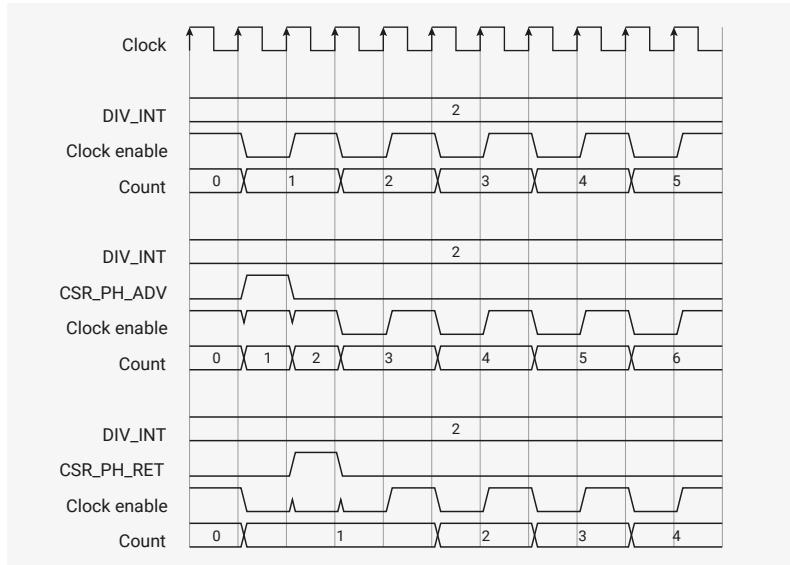
The figure consists of three vertically stacked timing diagrams. Each diagram shows a 'Clock' signal (a regular square wave), a 'DIV_INT' signal (a constant high level), and a 'Count' signal (a sequence of numbers 0 through 5 or 6). The 'Clock enable' signal is shown as a series of pulses that occur at specific clock cycles. In the first diagram, the clock enable is high for cycles 0, 1, 2, 3, 4, and 5. In the second diagram, the clock enable is high for cycles 0, 1, 2, 3, 4, 5, and 6. In the third diagram, the clock enable is high for cycles 0, 1, 2, 3, and 4. The 'Count' signal is shown as a sequence of numbers 0 through 5 or 6, with the count increasing by one for each clock cycle where the clock enable is high. The 'Clock enable' signal is controlled by the 'CSR_PH_ADV' and 'CSR_PH_RET' signals. In the first diagram, 'CSR_PH_ADV' is high for cycles 1 and 2, causing the clock enable to be high for those cycles. In the second diagram, 'CSR_PH_RET' is high for cycles 1 and 2, causing the clock enable to be low for those cycles. In the third diagram, 'CSR_PH_RET' is high for cycles 1 and 2, causing the clock enable to be low for those cycles.
The counter can not count faster than once per cycle, so PH_ADV requires DIV_INT > 1 or DIV_FRAC > 0. Likewise, the counter will not start to count backward if PH_RET is asserted when the clock enable is permanently low.
To advance or retard the phase by one count, software writes 1 to PH_ADV or PH_RET . Once an enable pulse has been inserted or deleted, the PH_ADV or PH_RET register bit will return to 0, and software can poll the CSR until this happens. PH_ADV will always insert a pulse into the next available gap, and PH_RET will always delete the next available pulse.
4.5.3. List of Registers
The PWM registers start at a base address of 0x40050000 (defined as PWM_BASE in SDK).
Table 516. List of PWM registers
| Offset | Name | Info |
|---|---|---|
| 0x00 | CH0_CSR | Control and status register |
| 0x04 | CH0_DIV | INT and FRAC form a fixed-point fractional number. Counting rate is system clock frequency divided by this number. Fractional division uses simple 1st-order sigma-delta. |
| 0x08 | CH0_CTR | Direct access to the PWM counter |
| 0x0c | CH0_CC | Counter compare values |
| 0x10 | CH0_TOP | Counter wrap value |
| 0x14 | CH1_CSR | Control and status register |
| 0x18 | CH1_DIV | INT and FRAC form a fixed-point fractional number. Counting rate is system clock frequency divided by this number. Fractional division uses simple 1st-order sigma-delta. |
| 0x1c | CH1_CTR | Direct access to the PWM counter |
| 0x20 | CH1_CC | Counter compare values |
| 0x24 | CH1_TOP | Counter wrap value |
| 0x28 | CH2_CSR | Control and status register |
| 0x2c | CH2_DIV | INT and FRAC form a fixed-point fractional number. Counting rate is system clock frequency divided by this number. Fractional division uses simple 1st-order sigma-delta. |
| Offset | Name | Info |
|---|---|---|
| 0x30 | CH2_CTR | Direct access to the PWM counter |
| 0x34 | CH2_CC | Counter compare values |
| 0x38 | CH2_TOP | Counter wrap value |
| 0x3c | CH3_CSR | Control and status register |
| 0x40 | CH3_DIV | INT and FRAC form a fixed-point fractional number. Counting rate is system clock frequency divided by this number. Fractional division uses simple 1st-order sigma-delta. |
| 0x44 | CH3_CTR | Direct access to the PWM counter |
| 0x48 | CH3_CC | Counter compare values |
| 0x4c | CH3_TOP | Counter wrap value |
| 0x50 | CH4_CSR | Control and status register |
| 0x54 | CH4_DIV | INT and FRAC form a fixed-point fractional number. Counting rate is system clock frequency divided by this number. Fractional division uses simple 1st-order sigma-delta. |
| 0x58 | CH4_CTR | Direct access to the PWM counter |
| 0x5c | CH4_CC | Counter compare values |
| 0x60 | CH4_TOP | Counter wrap value |
| 0x64 | CH5_CSR | Control and status register |
| 0x68 | CH5_DIV | INT and FRAC form a fixed-point fractional number. Counting rate is system clock frequency divided by this number. Fractional division uses simple 1st-order sigma-delta. |
| 0x6c | CH5_CTR | Direct access to the PWM counter |
| 0x70 | CH5_CC | Counter compare values |
| 0x74 | CH5_TOP | Counter wrap value |
| 0x78 | CH6_CSR | Control and status register |
| 0x7c | CH6_DIV | INT and FRAC form a fixed-point fractional number. Counting rate is system clock frequency divided by this number. Fractional division uses simple 1st-order sigma-delta. |
| 0x80 | CH6_CTR | Direct access to the PWM counter |
| 0x84 | CH6_CC | Counter compare values |
| 0x88 | CH6_TOP | Counter wrap value |
| 0x8c | CH7_CSR | Control and status register |
| 0x90 | CH7_DIV | INT and FRAC form a fixed-point fractional number. Counting rate is system clock frequency divided by this number. Fractional division uses simple 1st-order sigma-delta. |
| 0x94 | CH7_CTR | Direct access to the PWM counter |
| 0x98 | CH7_CC | Counter compare values |
| 0x9c | CH7_TOP | Counter wrap value |
| Offset | Name | Info |
|---|---|---|
| 0xa0 | EN | This register aliases the CSR_EN bits for all channels. Writing to this register allows multiple channels to be enabled or disabled simultaneously, so they can run in perfect sync. For each channel, there is only one physical EN register bit, which can be accessed through here or CHx_CSR. |
| 0xa4 | INTR | Raw Interrupts |
| 0xa8 | INTE | Interrupt Enable |
| 0xac | INTF | Interrupt Force |
| 0xb0 | INTS | Interrupt status after masking & forcing |
PWM: CH0_CSR, CH1_CSR, ..., CH6_CSR, CH7_CSR Registers
Offsets: 0x00, 0x14, ..., 0x78, 0x8c
Description
Control and status register
Table 517. CH0_CSR, CH1_CSR, ..., CH6_CSR, CH7_CSR Registers
| Bits | Description | Type | Reset |
|---|---|---|---|
| 31:8 | Reserved. | - | - |
| 7 | PH_ADV : Advance the phase of the counter by 1 count, while it is running. Self-clearing. Write a 1, and poll until low. Counter must be running at less than full speed ( \( \text{div\_int} + \text{div\_frac} / 16 > 1 \) ) | SC | 0x0 |
| 6 | PH_RET : Retard the phase of the counter by 1 count, while it is running. Self-clearing. Write a 1, and poll until low. Counter must be running. | SC | 0x0 |
| 5:4 | DIVMODE | RW | 0x0 |
| Enumerated values: | |||
| 0x0 → DIV: Free-running counting at rate dictated by fractional divider | |||
| 0x1 → LEVEL: Fractional divider operation is gated by the PWM B pin. | |||
| 0x2 → RISE: Counter advances with each rising edge of the PWM B pin. | |||
| 0x3 → FALL: Counter advances with each falling edge of the PWM B pin. | |||
| 3 | B_INV : Invert output B | RW | 0x0 |
| 2 | A_INV : Invert output A | RW | 0x0 |
| 1 | PH_CORRECT : 1: Enable phase-correct modulation. 0: Trailing-edge | RW | 0x0 |
| 0 | EN : Enable the PWM channel. | RW | 0x0 |
PWM: CH0_DIV, CH1_DIV, ..., CH6_DIV, CH7_DIV Registers
Offsets: 0x04, 0x18, ..., 0x7c, 0x90
Description
INT and FRAC form a fixed-point fractional number.
Counting rate is system clock frequency divided by this number.
Fractional division uses simple 1st-order sigma-delta.
Table 518. CH0_DIV, CH1_DIV, ..., CH6_DIV, CH7_DIV Registers
| Bits | Description | Type | Reset |
|---|---|---|---|
| 31:12 | Reserved. | - | - |
| 11:4 | INT | RW | 0x01 |
| 3:0 | FRAC | RW | 0x0 |
PWM: CH0_CTR, CH1_CTR, ..., CH6_CTR, CH7_CTR Registers
Offsets: 0x08, 0x1c, ..., 0x80, 0x94
Table 519. CH0_CTR, CH1_CTR, ..., CH6_CTR, CH7_CTR Registers
| Bits | Description | Type | Reset |
|---|---|---|---|
| 31:16 | Reserved. | - | - |
| 15:0 | Direct access to the PWM counter | RW | 0x0000 |
PWM: CH0_CC, CH1_CC, ..., CH6_CC, CH7_CC Registers
Offsets: 0x0c, 0x20, ..., 0x84, 0x98
Description
Counter compare values
Table 520. CH0_CC, CH1_CC, ..., CH6_CC, CH7_CC Registers
| Bits | Description | Type | Reset |
|---|---|---|---|
| 31:16 | B | RW | 0x0000 |
| 15:0 | A | RW | 0x0000 |
PWM: CH0_TOP, CH1_TOP, ..., CH6_TOP, CH7_TOP Registers
Offsets: 0x10, 0x24, ..., 0x88, 0x9c
Table 521. CH0_TOP, CH1_TOP, ..., CH6_TOP, CH7_TOP Registers
| Bits | Description | Type | Reset |
|---|---|---|---|
| 31:16 | Reserved. | - | - |
| 15:0 | Counter wrap value | RW | 0xffff |
PWM: EN Register
Offset: 0xa0
Description
This register aliases the CSR_EN bits for all channels.
Writing to this register allows multiple channels to be enabled or disabled simultaneously, so they can run in perfect sync.
For each channel, there is only one physical EN register bit, which can be accessed through here or CHx_CSR.
Table 522. EN Register
| Bits | Description | Type | Reset |
|---|---|---|---|
| 31:8 | Reserved. | - | - |
| 7 | CH7 | RW | 0x0 |
| 6 | CH6 | RW | 0x0 |
| 5 | CH5 | RW | 0x0 |
| 4 | CH4 | RW | 0x0 |
| 3 | CH3 | RW | 0x0 |
| Bits | Description | Type | Reset |
|---|---|---|---|
| 2 | CH2 | RW | 0x0 |
| 1 | CH1 | RW | 0x0 |
| 0 | CH0 | RW | 0x0 |
PWM: INTR Register
Offset: 0xa4
Description
Raw Interrupts
Table 523. INTR Register
| Bits | Description | Type | Reset |
|---|---|---|---|
| 31:8 | Reserved. | - | - |
| 7 | CH7 | WC | 0x0 |
| 6 | CH6 | WC | 0x0 |
| 5 | CH5 | WC | 0x0 |
| 4 | CH4 | WC | 0x0 |
| 3 | CH3 | WC | 0x0 |
| 2 | CH2 | WC | 0x0 |
| 1 | CH1 | WC | 0x0 |
| 0 | CH0 | WC | 0x0 |
PWM: INTE Register
Offset: 0xa8
Description
Interrupt Enable
Table 524. INTE Register
| Bits | Description | Type | Reset |
|---|---|---|---|
| 31:8 | Reserved. | - | - |
| 7 | CH7 | RW | 0x0 |
| 6 | CH6 | RW | 0x0 |
| 5 | CH5 | RW | 0x0 |
| 4 | CH4 | RW | 0x0 |
| 3 | CH3 | RW | 0x0 |
| 2 | CH2 | RW | 0x0 |
| 1 | CH1 | RW | 0x0 |
| 0 | CH0 | RW | 0x0 |
PWM: INTF Register
Offset: 0xac
Description
Interrupt Force
Table 525. INTF Register
| Bits | Description | Type | Reset |
|---|---|---|---|
| 31:8 | Reserved. | - | - |
| 7 | CH7 | RW | 0x0 |
| 6 | CH6 | RW | 0x0 |
| 5 | CH5 | RW | 0x0 |
| 4 | CH4 | RW | 0x0 |
| 3 | CH3 | RW | 0x0 |
| 2 | CH2 | RW | 0x0 |
| 1 | CH1 | RW | 0x0 |
| 0 | CH0 | RW | 0x0 |
PWM: INTS Register
Offset: 0xb0
Description
Interrupt status after masking & forcing
Table 526. INTS Register
| Bits | Description | Type | Reset |
|---|---|---|---|
| 31:8 | Reserved. | - | - |
| 7 | CH7 | RO | 0x0 |
| 6 | CH6 | RO | 0x0 |
| 5 | CH5 | RO | 0x0 |
| 4 | CH4 | RO | 0x0 |
| 3 | CH3 | RO | 0x0 |
| 2 | CH2 | RO | 0x0 |
| 1 | CH1 | RO | 0x0 |
| 0 | CH0 | RO | 0x0 |
4.6. Timer
4.6.1. Overview
The system timer peripheral on RP2040 provides a global microsecond timebase for the system, and generates interrupts based on this timebase. It supports the following features:
- • A single 64-bit counter, incrementing once per microsecond
- • This counter can be read from a pair of latching registers, for race-free reads over a 32-bit bus.
- • Four alarms: match on the lower 32 bits of counter, IRQ on match.
The timer uses a one microsecond reference that is generated in the Watchdog (see Section 4.7.2 ), and derived from
the reference clock (Figure 28), which itself is usually connected directly to the crystal oscillator (Section 2.16).
The 64-bit counter effectively can not overflow (thousands of years at 1MHz), so the system timer is completely monotonic in practice.
4.6.1.1. Other Timer Resources on RP2040
The system timer is intended to provide a global timebase for software. RP2040 has a number of other programmable counter resources which can provide regular interrupts, or trigger DMA transfers.
- • The PWM (Section 4.5) contains 8× 16-bit programmable counters, which run at up to system speed, can generate interrupts, and can be continuously reprogrammed via the DMA, or trigger DMA transfers to other peripherals.
- • 8× PIO state machines (Chapter 3) can count 32-bit values at system speed, and generate interrupts.
- • The DMA (Section 2.5) has four internal pacing timers, which trigger transfers at regular intervals.
- • Each Cortex-M0+ core (Section 2.4) has a standard 24-bit SysTick timer, counting either the microsecond tick (Section 4.7.2) or the system clock.
4.6.2. Counter
The timer has a 64-bit counter, but RP2040 only has a 32-bit data bus. This means that the TIME value is accessed through a pair of registers. These are:
- • TIMEHW and TIMELW to write the time
- • TIMEHR and TIMELR to read the time
These pairs are used by accessing the lower register, L , followed by the higher register, H . In the read case, reading the L register latches the value in the H register so that an accurate time can be read. Alternatively, TIMERAWH and TIMERAWL can be used to read the raw time without any latching.
⚠ CAUTION
While it is technically possible to force a new time value by writing to the TIMEHW and TIMELW registers, programmers are discouraged from doing this. This is because the timer value is expected to be monotonically increasing by the SDK which uses it for timeouts, elapsed time etc.
4.6.3. Alarms
The timer has 4 alarms, and outputs a separate interrupt for each alarm. The alarms match on the lower 32 bits of the 64-bit counter which means they can be fired at a maximum of \( 2^{32} \) microseconds into the future. This is equivalent to:
- • \( 2^{32} \div 10^6 \) : ~4295 seconds
- • \( 4295 \div 60 \) : ~72 minutes
i NOTE
This timer is expected to be used for short sleeps. If you want a longer alarm see Section 4.8.
To enable an alarm:
- • Enable the interrupt at the timer with a write to the appropriate alarm bit in INTE : i.e. \( (1 \ll 0) \) for ALARM0
- • Enable the appropriate timer interrupt at the processor (see Section 2.3.2)
- • Write the time you would like the interrupt to fire to ALARM0 (i.e. the current value in TIMERAWL plus your desired alarm time in microseconds). Writing the time to the ALARM register sets the ARMED bit as a side effect.
Once the alarm has fired, the ARMED bit will be set to 0 . To clear the latched interrupt, write a 1 to the appropriate bit in INTR .
4.6.4. Programmer's Model
i NOTE
The Watchdog tick (see Section 4.7.2 ) must be running for the timer to start counting. The SDK starts this tick as part of the platform initialisation code.
4.6.4.1. Reading the time
i NOTE
Time here refers to the number of microseconds since the timer was started, it is not a clock. For that - see Section 4.8 .
The simplest form of reading the 64-bit time is to read TIMELR followed by TIMEHR . However, because RP2040 has 2 cores, it is unsafe to do this if the second core is executing code that can also access the timer, or if the timer is read concurrently in an IRQ handler and in thread mode. This is because reading TIMELR latches the value in TIMEHR (i.e. stops it updating) until TIMEHR is read. If one core reads TIMELR followed by another core reading TIMELR , the value in TIMEHR isn't necessarily accurate. The example below shows the simplest form of getting the 64-bit time.
Pico Examples: https://github.com/raspberrypi/pico-examples/blob/master/timer/timer_lowlevel/timer_lowlevel.c Lines 15 - 23
15 // Simplest form of getting 64 bit time from the timer.
16 // It isn't safe when called from 2 cores because of the latching
17 // so isn't implemented this way in the sdk
18 static uint64_t get_time(void) {
19     // Reading low latches the high value
20     uint32_t lo = timer_hw->timelr;
21     uint32_t hi = timer_hw->timehr;
22     return ((uint64_t) hi << 32u) | lo;
23 }
The SDK provides a time_us_64 function that uses a more thorough method to get the 64-bit time, which makes use of the TIMERAWH and TIMERAWL registers. The RAW registers don't latch, and therefore make time_us_64 safe to call from multiple cores at once.
SDK: https://github.com/raspberrypi/pico-sdk/blob/master/src/rp2_common/hardware_timer/timer.c Lines 57 - 73
57 uint64_t timer_time_us_64(timer_hw_t *timer) {
58     // Need to make sure that the upper 32 bits of the timer
59     // don't change, so read that first
60     uint32_t hi = timer->timerawh;
61     uint32_t lo;
62     do {
63         // Read the lower 32 bits
64         lo = timer->timerawl;
65         // Now read the upper 32 bits again and
66         // check that it hasn't incremented. If it has loop around
67         // and read the lower 32 bits again to get an accurate value
68         uint32_t next_hi = timer->timerawh;
69         if (hi == next_hi) break;
70         hi = next_hi;
71 } while (true); 72 return ((uint64_t) hi << 32u) | lo; 73 }
4.6.4.2. Set an alarm
The standalone timer example,
timer_lowlevel
, demonstrates how to set an alarm at a hardware level, without the additional abstraction over the timer that the SDK provides. To use these abstractions see
Section 4.6.4.4
.
Pico Examples: https://github.com/raspberrypi/pico-examples/blob/master/timer/timer_lowlevel/timer_lowlevel.c Lines 27 - 74
27 // Use alarm 0
28 #define ALARM_NUM 0
29 #define ALARM_IRQ timer_hardware_alarm_get_irq_num(timer_hw, ALARM_NUM)
30
31 // Alarm interrupt handler
32 static volatile bool alarm_fired;
33
34 static void alarm_irq(void) {
35     // Clear the alarm irq
36     hw_clear_bits(&timer_hw->intr, 1u << ALARM_NUM);
37
38     // Assume alarm 0 has fired
39     printf("Alarm IRQ fired\n");
40     alarm_fired = true;
41 }
42
43 static void alarm_in_us(uint32_t delay_us) {
44     // Enable the interrupt for our alarm (the timer outputs 4 alarm irqs)
45     hw_set_bits(&timer_hw->inte, 1u << ALARM_NUM);
46     // Set irq handler for alarm irq
47     irq_set_exclusive_handler(ALARM_IRQ, alarm_irq);
48     // Enable the alarm irq
49     irq_set_enabled(ALARM_IRQ, true);
50     // Enable interrupt in block and at processor
51
52     // Alarm is only 32 bits so if trying to delay more
53     // than that need to be careful and keep track of the upper
54     // bits
55     uint64_t target = timer_hw->timerawl + delay_us;
56
57     // Write the lower 32 bits of the target time to the alarm which
58     // will arm it
59     timer_hw->alarm[ALARM_NUM] = (uint32_t) target;
60 }
61
62 int main() {
63     stdio_init_all();
64     printf("Timer lowlevel!\n");
65
66     // Set alarm every 2 seconds
67     while (1) {
68         alarm_fired = false;
69         alarm_in_us(1000000 * 2);
70         // Wait for alarm to fire
71         while (!alarm_fired);
72     }
73 }
4.6.4.3. Busy wait
If you don't want to use an alarm to wait for a period of time, instead use a while loop. The SDK provides various
busy_wait_
functions to do this:
SDK: https://github.com/raspberrypi/pico-sdk/blob/master/src/rp2_common/hardware_timer/timer.c Lines 77 - 122
77 void timer_busy_wait_us_32(timer_hw_t *timer, uint32_t delay_us) {
78     if (0 <= (int32_t)delay_us) {
79         // we only allow 31 bits, otherwise we could have a race in the loop below with
80         // values very close to 2^32
81         uint32_t start = timer->timerawl;
82         while (timer->timerawl - start < delay_us) {
83             tight_loop_contents();
84         }
85     } else {
86         busy_wait_us(delay_us);
87     }
88 }
89
90 void timer_busy_wait_us(timer_hw_t *timer, uint64_t delay_us) {
91     uint64_t base = timer_time_us_64(timer);
92     uint64_t target = base + delay_us;
93     if (target < base) {
94         target = (uint64_t)-1;
95     }
96     absolute_time_t t;
97     update_us_since_boot(&t, target);
98     timer_busy_wait_until(timer, t);
99 }
100
101 void timer_busy_wait_ms(timer_hw_t *timer, uint32_t delay_ms)
102 {
103     if (delay_ms <= 0x7fffffffu / 1000) {
104         timer_busy_wait_us_32(timer, delay_ms * 1000);
105     } else {
106         timer_busy_wait_us(timer, delay_ms * 1000ull);
107     }
108 }
109
110 void timer_busy_wait_until(timer_hw_t *timer, absolute_time_t t) {
111     uint64_t target = to_us_since_boot(t);
112     uint32_t hi_target = (uint32_t)(target >> 32u);
113     uint32_t hi = timer->timerawh;
114     while (hi < hi_target) {
115         hi = timer->timerawh;
116         tight_loop_contents();
117     }
118     while (hi == hi_target && timer->timerawl < (uint32_t) target) {
119         hi = timer->timerawh;
120         tight_loop_contents();
121     }
122 }
4.6.4.4. Complete example using SDK
Pico Examples: https://github.com/raspberrypi/pico-examples/blob/master/timer/hello_timer/hello_timer.c Lines 11 - 57
11 volatile bool timer_fired = false;
12
13 int64_t alarm_callback(alarm_id_t id, __unused void *user_data) {
14     printf("Timer %d fired!\n", (int) id);
15     timer_fired = true;
16     // Can return a value here in us to fire in the future
17     return 0;
18 }
19
20 bool repeating_timer_callback(__unused struct repeating_timer *t) {
21     printf("Repeat at %lld\n", time_us_64());
22     return true;
23 }
24
25 int main() {
26     stdio_init_all();
27     printf("Hello Timer!\n");
28
29     // Call alarm_callback in 2 seconds
30     add_alarm_in_ms(2000, alarm_callback, NULL, false);
31
32     // Wait for alarm callback to set timer_fired
33     while (!timer_fired) {
34         tight_loop_contents();
35     }
36
37     // Create a repeating timer that calls repeating_timer_callback.
38     // If the delay is > 0 then this is the delay between the previous callback ending and the
39     // next starting.
40     // If the delay is negative (see below) then the next call to the callback will be exactly
41     // 500ms after the
42     // start of the call to the last callback
43     struct repeating_timer timer;
44     add_repeating_timer_ms(500, repeating_timer_callback, NULL, &timer);
45     sleep_ms(3000);
46     bool cancelled = cancel_repeating_timer(&timer);
47     printf("cancelled... %d\n", cancelled);
48     sleep_ms(2000);
49
50     // Negative delay so means we will call repeating_timer_callback, and call it again
51     // 500ms later regardless of how long the callback took to execute
52     add_repeating_timer_ms(-500, repeating_timer_callback, NULL, &timer);
53     sleep_ms(3000);
54     cancelled = cancel_repeating_timer(&timer);
55     printf("cancelled... %d\n", cancelled);
56     sleep_ms(2000);
57     printf("Done\n");
58     return 0;
59 }
4.6.5. List of Registers
The Timer registers start at a base address of 0x40054000 (defined as
TIMER_BASE
in SDK).
Table 527. List of
TIMER registers
| Offset | Name | Info |
|---|---|---|
| 0x00 | TIMEHW | Write to bits 63:32 of time always write timelw before timehw |
| Offset | Name | Info |
|---|---|---|
| 0x04 | TIMELW | Write to bits 31:0 of time writes do not get copied to time until timehw is written |
| 0x08 | TIMEHR | Read from bits 63:32 of time always read timelr before timehr |
| 0x0c | TIMELR | Read from bits 31:0 of time |
| 0x10 | ALARM0 | Arm alarm 0, and configure the time it will fire. Once armed, the alarm fires when TIMER_ALARM0 == TIMELR
.The alarm will disarm itself once it fires, and can be disarmed early using the ARMED status register. |
| 0x14 | ALARM1 | Arm alarm 1, and configure the time it will fire. Once armed, the alarm fires when TIMER_ALARM1 == TIMELR
.The alarm will disarm itself once it fires, and can be disarmed early using the ARMED status register. |
| 0x18 | ALARM2 | Arm alarm 2, and configure the time it will fire. Once armed, the alarm fires when TIMER_ALARM2 == TIMELR
.The alarm will disarm itself once it fires, and can be disarmed early using the ARMED status register. |
| 0x1c | ALARM3 | Arm alarm 3, and configure the time it will fire. Once armed, the alarm fires when TIMER_ALARM3 == TIMELR
.The alarm will disarm itself once it fires, and can be disarmed early using the ARMED status register. |
| 0x20 | ARMED | Indicates the armed/disarmed status of each alarm. A write to the corresponding ALARMx register arms the alarm. Alarms automatically disarm upon firing, but writing ones here will disarm immediately without waiting to fire. |
| 0x24 | TIMERAWH | Raw read from bits 63:32 of time (no side effects) |
| 0x28 | TIMERAWL | Raw read from bits 31:0 of time (no side effects) |
| 0x2c | DBGPAUSE | Set bits high to enable pause when the corresponding debug ports are active |
| 0x30 | PAUSE | Set high to pause the timer |
| 0x34 | INTR | Raw Interrupts |
| 0x38 | INTE | Interrupt Enable |
| 0x3c | INTF | Interrupt Force |
| 0x40 | INTS | Interrupt status after masking & forcing |
TIMER: TIMEHW Register
Offset: 0x00
Table 528. TIMEHW Register
| Bits | Description | Type | Reset |
|---|---|---|---|
| 31:0 | Write to bits 63:32 of time always write timelw before timehw | WF | 0x00000000 |
TIMER: TIMELW Register
Offset: 0x04
Table 529. TIMELW Register
| Bits | Description | Type | Reset |
|---|---|---|---|
| 31:0 | Write to bits 31:0 of time writes do not get copied to time until timehw is written | WF | 0x00000000 |
TIMER: TIMEHR Register
Offset: 0x08
Table 530. TIMEHR Register
| Bits | Description | Type | Reset |
|---|---|---|---|
| 31:0 | Read from bits 63:32 of time always read timelr before timehr | RO | 0x00000000 |
TIMER: TIMELR Register
Offset: 0x0c
Table 531. TIMELR Register
| Bits | Description | Type | Reset |
|---|---|---|---|
| 31:0 | Read from bits 31:0 of time | RO | 0x00000000 |
TIMER: ALARM0 Register
Offset: 0x10
Table 532. ALARM0 Register
| Bits | Description | Type | Reset |
|---|---|---|---|
| 31:0 | Arm alarm 0, and configure the time it will fire. Once armed, the alarm fires when TIMER_ALARM0 == TIMELR. The alarm will disarm itself once it fires, and can be disarmed early using the ARMED status register. | RW | 0x00000000 |
TIMER: ALARM1 Register
Offset: 0x14
Table 533. ALARM1 Register
| Bits | Description | Type | Reset |
|---|---|---|---|
| 31:0 | Arm alarm 1, and configure the time it will fire. Once armed, the alarm fires when TIMER_ALARM1 == TIMELR. The alarm will disarm itself once it fires, and can be disarmed early using the ARMED status register. | RW | 0x00000000 |
TIMER: ALARM2 Register
Offset: 0x18
Table 534. ALARM2 Register
| Bits | Description | Type | Reset |
|---|---|---|---|
| 31:0 | Arm alarm 2, and configure the time it will fire. Once armed, the alarm fires when TIMER_ALARM2 == TIMELR
.The alarm will disarm itself once it fires, and can be disarmed early using the ARMED status register. | RW | 0x00000000 |
TIMER: ALARM3 Register
Offset: 0x1c
Table 535. ALARM3 Register
| Bits | Description | Type | Reset |
|---|---|---|---|
| 31:0 | Arm alarm 3, and configure the time it will fire. Once armed, the alarm fires when TIMER_ALARM3 == TIMELR
.The alarm will disarm itself once it fires, and can be disarmed early using the ARMED status register. | RW | 0x00000000 |
TIMER: ARMED Register
Offset: 0x20
Table 536. ARMED Register
| Bits | Description | Type | Reset |
|---|---|---|---|
| 31:4 | Reserved. | - | - |
| 3:0 | Indicates the armed/disarmed status of each alarm. A write to the corresponding ALARMx register arms the alarm. Alarms automatically disarm upon firing, but writing ones here will disarm immediately without waiting to fire. | WC | 0x0 |
TIMER: TIMERAWH Register
Offset: 0x24
Table 537. TIMERAWH Register
| Bits | Description | Type | Reset |
|---|---|---|---|
| 31:0 | Raw read from bits 63:32 of time (no side effects) | RO | 0x00000000 |
TIMER: TIMERAWL Register
Offset: 0x28
Table 538. TIMERAWL Register
| Bits | Description | Type | Reset |
|---|---|---|---|
| 31:0 | Raw read from bits 31:0 of time (no side effects) | RO | 0x00000000 |
TIMER: DBGPAUSE Register
Offset: 0x2c
Description
Set bits high to enable pause when the corresponding debug ports are active
Table 539. DBGPAUSE Register
| Bits | Description | Type | Reset |
|---|---|---|---|
| 31:3 | Reserved. | - | - |
| 2 | DBG1 : Pause when processor 1 is in debug mode | RW | 0x1 |
| 1 | DBG0 : Pause when processor 0 is in debug mode | RW | 0x1 |
| Bits | Description | Type | Reset |
|---|---|---|---|
| 0 | Reserved. | - | - |
TIMER: PAUSE Register
Offset: 0x30
Table 540. PAUSE Register
| Bits | Description | Type | Reset |
|---|---|---|---|
| 31:1 | Reserved. | - | - |
| 0 | Set high to pause the timer | RW | 0x0 |
TIMER: INTR Register
Offset: 0x34
Description
Raw Interrupts
Table 541. INTR Register
| Bits | Description | Type | Reset |
|---|---|---|---|
| 31:4 | Reserved. | - | - |
| 3 | ALARM_3 | WC | 0x0 |
| 2 | ALARM_2 | WC | 0x0 |
| 1 | ALARM_1 | WC | 0x0 |
| 0 | ALARM_0 | WC | 0x0 |
TIMER: INTE Register
Offset: 0x38
Description
Interrupt Enable
Table 542. INTE Register
| Bits | Description | Type | Reset |
|---|---|---|---|
| 31:4 | Reserved. | - | - |
| 3 | ALARM_3 | RW | 0x0 |
| 2 | ALARM_2 | RW | 0x0 |
| 1 | ALARM_1 | RW | 0x0 |
| 0 | ALARM_0 | RW | 0x0 |
TIMER: INTF Register
Offset: 0x3c
Description
Interrupt Force
Table 543. INTF Register
| Bits | Description | Type | Reset |
|---|---|---|---|
| 31:4 | Reserved. | - | - |
| 3 | ALARM_3 | RW | 0x0 |
| Offset 0x0 0x4 0x8 0xc Bits | Name FRCE_ON FRCE_OFF WDSEL DONE Description | Info Force block out of reset (i.e. power it on) Force into reset (i.e. power it off) Set to 1 if this peripheral should be reset when the watchdog Indicates the peripheral’s registers are ready to access. Type | Reset |
|---|---|---|---|
| 31:4 | Reserved. | - | - |
| 3 | ALARM_3 | RO | 0x0 |
| 2 | ALARM_2 | RO | 0x0 |
| 1 | ALARM_1 | RO | 0x0 |
| 0 | ALARM_0 | RO | 0x0 |
| stop it from reaching zero. The watchdog is reset by rst_n_run | , which is deasserted as soon as the digital core supply (DVDD) is powered and | ||
| 2.13) | and reset controller (see Section 2.14 register exists in both the power-on state machine and reset controller. | ), resetting their dependants if they are selected in the | Section WDSEL register. The |
| 4.7.2. Tick generation The watchdog reference clock, clk_tick | , is driven from clk_ref . Ideally clk_ref | will be configured to use the Crystal | |
| Oscillator ( | Section 2.16 | ) so that it provides an accurate reference clock. The reference clock is divided internally to | |
| generate a tick (nominally 1 μ | s) to use as the watchdog tick. The tick is configured using the | TICK register. | |
| To avoid duplicating logic, this tick is also distributed to the timer (see | Section 4.6) | and used as the timer reference. | |
| 17 | watchdog_start_tick(uint cycles) { tick_start(TICK_WATCHDOG, cycles); |
TIMER: INTS Register
Offset: 0x40
Description
Interrupt status after masking & forcing
Table 544. INTS Register
4.7. Watchdog
4.7.1. Overview
The watchdog is a countdown timer that can restart parts of the chip if it reaches zero. This can be used to restart the processor if software gets stuck in an infinite loop. The programmer must periodically write a value to the watchdog to stop it from reaching zero.
The watchdog is reset by
rst_n_run
, which is deasserted as soon as the digital core supply (DVDD) is powered and stable, and the RUN pin is high. This allows the watchdog reset to feed into the power-on state machine (see
Section 2.13
) and reset controller (see
Section 2.14
), resetting their dependants if they are selected in the
WDSEL
register. The
WDSEL
register exists in both the power-on state machine and reset controller.
4.7.2. Tick generation
The watchdog reference clock,
clk_tick
, is driven from
clk_ref
. Ideally
clk_ref
will be configured to use the Crystal Oscillator (
Section 2.16
) so that it provides an accurate reference clock. The reference clock is divided internally to generate a tick (nominally 1µs) to use as the watchdog tick. The tick is configured using the
TICK
register.
i NOTE
To avoid duplicating logic, this tick is also distributed to the timer (see Section 4.6 ) and used as the timer reference.
The SDK starts the watchdog tick in
clocks_init
:
SDK: https://github.com/raspberrypi/pico-sdk/blob/master/src/rp2_common/hardware_watchdog/watchdog.c Lines 16 - 18
16 void watchdog_start_tick(uint cycles) {
17     tick_start(TICK_WATCHDOG, cycles);
18 }
4.7.3. Watchdog Counter
The watchdog counter is loaded by the LOAD register. The current value can be seen in CTRL.TIME .
⚠ WARNING
Due to a logic error, the watchdog counter is decremented twice per tick. Which means the programmer needs to program double the intended count down value. The SDK examples take this issue into account. See RP2040-E1 for more information.
4.7.4. Scratch Registers
The watchdog contains eight 32-bit scratch registers that can be used to store information between soft resets of the chip. A
rst_n_run
event triggered by toggling the RUN pin or cycling the digital core supply (DVDD) will reset the scratch registers.
The bootrom checks the watchdog scratch registers for a magic number on boot. This can be used to soft reset the chip into some user specified code. See Section 2.8.1.1 for more information.
4.7.5. Programmer's Model
The SDK provides a
hardware_watchdog
driver to control the watchdog.
4.7.5.1. Enabling the watchdog
SDK: https://github.com/raspberrypi/pico-sdk/blob/master/src/rp2_common/hardware_watchdog/watchdog.c Lines 42 - 74
42 // Helper function used by both watchdog_enable and watchdog_reboot
43 void _watchdog_enable(uint32_t delay_ms, bool pause_on_debug) {
44     valid_params_if(HARDWARE_WATCHDOG, delay_ms <= WATCHDOG_LOAD_BITS / (1000 *
        WATCHDOG_XFACTOR));
45     hw_clear_bits(&watchdog_hw->ctrl, WATCHDOG_CTRL_ENABLE_BITS);
46
47     // Reset everything apart from ROSC and XOSC
48     hw_set_bits(&psm_hw->wdsel, PSM_WDSEL_BITS & ~(PSM_WDSEL_ROSC_BITS |
        PSM_WDSEL_XOSC_BITS));
49
50     uint32_t dbg_bits = WATCHDOG_CTRL_PAUSE_DBG0_BITS |
51                         WATCHDOG_CTRL_PAUSE_DBG1_BITS |
52                         WATCHDOG_CTRL_PAUSE_JTAG_BITS;
53
54     if (pause_on_debug) {
55         hw_set_bits(&watchdog_hw->ctrl, dbg_bits);
56     } else {
57         hw_clear_bits(&watchdog_hw->ctrl, dbg_bits);
58     }
59
60     if (!delay_ms) {
61         hw_set_bits(&watchdog_hw->ctrl, WATCHDOG_CTRL_TRIGGER_BITS);
62     } else {
63         load_value = delay_ms * 1000;
64         load_value *= 2;
65 if (load_value > WATCHDOG_LOAD_BITS) 66 load_value = WATCHDOG_LOAD_BITS; 67 68 watchdog_update(); 69 70 hw_set_bits(&watchdog_hw->ctrl, WATCHDOG_CTRL_ENABLE_BITS); 71 } 72 }
4.7.5.2. Updating the watchdog counter
SDK: https://github.com/raspberrypi/pico-sdk/blob/master/src/rp2_common/hardware_watchdog/watchdog.c Lines 24 - 28
24 static uint32_t load_value;
25
26 void watchdog_update(void) {
27     watchdog_hw->load = load_value;
28 }
4.7.5.3. Usage
The Pico Examples repository provides a
hello_watchdog
example that uses the
hardware_watchdog
to demonstrate use of the watchdog.
Pico Examples: https://github.com/raspberrypi/pico-examples/blob/master/watchdog/hello_watchdog/hello_watchdog.c Lines 11 - 33
11 int main() {
12     stdio_init_all();
13
14     if (watchdog_enable_caused_reboot()) {
15         printf("Rebooted by Watchdog!\n");
16         return 0;
17     } else {
18         printf("Clean boot\n");
19     }
20
21     // Enable the watchdog, requiring the watchdog to be updated every 100ms or the chip will
    reboot
22     // second arg is pause on debug which means the watchdog will pause when stepping through
    code
23     watchdog_enable(100, 1);
24
25     for (uint i = 0; i < 5; i++) {
26         printf("Updating watchdog %d\n", i);
27         watchdog_update();
28     }
29
30     // Wait in an infinite loop and don't update the watchdog so it reboots us
31     printf("Waiting to be rebooted by watchdog\n");
32     while(1);
33 }
4.7.6. List of Registers
The watchdog registers start at a base address of 0x40058000 (defined as WATCHDOG_BASE in SDK).
Table 545. List of WATCHDOG registers
| Offset | Name | Info |
|---|---|---|
| 0x00 | CTRL | Watchdog control |
| 0x04 | LOAD | Load the watchdog timer. |
| 0x08 | REASON | Logs the reason for the last reset. |
| 0x0c | SCRATCH0 | Scratch register |
| 0x10 | SCRATCH1 | Scratch register |
| 0x14 | SCRATCH2 | Scratch register |
| 0x18 | SCRATCH3 | Scratch register |
| 0x1c | SCRATCH4 | Scratch register |
| 0x20 | SCRATCH5 | Scratch register |
| 0x24 | SCRATCH6 | Scratch register |
| 0x28 | SCRATCH7 | Scratch register |
| 0x2c | TICK | Controls the tick generator |
WATCHDOG: CTRL Register
Offset: 0x00
Description
- Watchdog control
- The rst_wdsel register determines which subsystems are reset when the watchdog is triggered.
- The watchdog can be triggered in software.
Table 546. CTRL Register
| Bits | Description | Type | Reset |
|---|---|---|---|
| 31 | TRIGGER: Trigger a watchdog reset | SC | 0x0 |
| 30 | ENABLE: When not enabled the watchdog timer is paused | RW | 0x0 |
| 29:27 | Reserved. | - | - |
| 26 | PAUSE_DBG1: Pause the watchdog timer when processor 1 is in debug mode | RW | 0x1 |
| 25 | PAUSE_DBG0: Pause the watchdog timer when processor 0 is in debug mode | RW | 0x1 |
| 24 | PAUSE_JTAG: Pause the watchdog timer when JTAG is accessing the bus fabric | RW | 0x1 |
| 23:0 | TIME: Indicates the number of ticks / 2 (see errata RP2040-E1) before a watchdog reset will be triggered | RO | 0x000000 |
WATCHDOG: LOAD Register
Offset: 0x04
Table 547. LOAD Register
| Bits | Description | Type | Reset |
|---|---|---|---|
| 31:24 | Reserved. | - | - |
| 23:0 | Load the watchdog timer. The maximum setting is 0xffffff which corresponds to 0xffffff / 2 ticks before triggering a watchdog reset (see errata RP2040-E1). | WF | 0x000000 |
WATCHDOG: REASON Register
Offset: 0x08
Description
Logs the reason for the last reset. Both bits are zero for the case of a hardware reset.
Table 548. REASON Register
| Bits | Description | Type | Reset |
|---|---|---|---|
| 31:2 | Reserved. | - | - |
| 1 | FORCE | RO | 0x0 |
| 0 | TIMER | RO | 0x0 |
WATCHDOG: SCRATCH0, SCRATCH1, ..., SCRATCH6, SCRATCH7 Registers
Offsets: 0x0c, 0x10, ..., 0x24, 0x28
Table 549. SCRATCH0, SCRATCH1, ..., SCRATCH6, SCRATCH7 Registers
| Bits | Description | Type | Reset |
|---|---|---|---|
| 31:0 | Scratch register. Information persists through soft reset of the chip. | RW | 0x00000000 |
WATCHDOG: TICK Register
Offset: 0x2c
Description
Controls the tick generator
Table 550. TICK Register
| Bits | Description | Type | Reset |
|---|---|---|---|
| 31:20 | Reserved. | - | - |
| 19:11 | COUNT : Count down timer: the remaining number clk_tick cycles before the next tick is generated. | RO | - |
| 10 | RUNNING : Is the tick generator running? | RO | - |
| 9 | ENABLE : start / stop tick generation | RW | 0x1 |
| 8:0 | CYCLES : Total number of clk_tick cycles before the next tick. | RW | 0x000 |
4.8. RTC
The Real-time Clock (RTC) provides time in human-readable format and can be used to generate interrupts at specific times.
4.8.1. Storage Format
Time is stored in binary, separated in seven fields:
Table 551. RTC storage format
| Date/Time Field | Size | Legal values |
|---|---|---|
| Year | 12 bits | 0..4095 |
| Month | 4 bits | 1..12 |
| Day | 5 bits | 1..[28,29,30,31], depending on the month |
| Day of Week | 3 bits | 0..6. Sunday = 0 |
| Hour | 5 bits | 0..23 |
| Minute | 6 bits | 0..59 |
| Seconds | 6 bits | 0..59 |
The RTC does not check that the programmed values are in range. Illegal values may cause unexpected behaviour.
4.8.1.1. Day of the week
Day of the week is encoded as Sun 0, Mon 1, ..., Sat 6 (i.e. ISO8601 mod 7).
There is no built-in calendar function. The RTC will not compute the correct day of the week; it will only increment the existing value.
4.8.2. Leap year
If the current value of YEAR in SETUP_0 is evenly divisible by 4, a leap year is detected, and Feb 28th is followed by Feb 29th instead of March 1st. Since this is not always true (century years for example), the leap year checking can be forced off by setting CTRL.FORCE_NOTLEAPYEAR .
NOTE
The leap year check is done only when needed (the second following Feb 28, 23:59:59). The software can set FORCE_NOTLEAPYEAR anytime after 2096 Mar 1 00:00:00 as long as it arrives before 2100 Feb 28 23:59:59 (i.e. taking into account the clock domain crossing latency)
4.8.3. Interrupts
The RTC can generate an interrupt at a configured time. There is a global bit, MATCH_ENA in IRQ_SETUP_0 to enable this feature, and individual enables for each time field (year, month, day, day-of-the-week, hour, minute, second). The individual enables can be used to implement repeating interrupts at specified times.
The alarm interrupt is sent to the processors and also to the ROSC and XOSC to wake them from dormant mode. See Section 4.8.5.5 for more information on dormant mode.
4.8.4. Reference clock
The RTC uses a reference clock clk_rtc , which should be any integer frequency in the range 1...65536Hz.
The internal 1Hz reference is created by an internal clock divider which divides clk_rtc by an integer value. The divide value minus 1 is set in CLKDIV_M1 .
⚠ WARNINGWhile it is possible to change
CLKDIV_M1
while the RTC is enabled, it is not recommended.
clk_rtc
can be driven either from an internal or external clock source. Those sources can be prescaled, using a fractional divider (see
Section 2.15
).
Examples of possible clock sources include:
- • XOSC @ 12MHz / 256 = 46875Hz. To get a 1Hz reference
CLKDIV_M1should be set to 46874. - • An external reference from a GPS, which generates one pulse per second. Configure
clk_rtcto run from the GPIN0 clock source from GPIO pin 20. In this case, theclk_rtcdivider is 1 and the internal RTC clock divider is also 1 (i.e.CLKDIV_M1 = 0).
All RTC register reads and writes are done from the processor clock domain
clk_sys
. All data are synchronised back and forth between the domains. Writing to the RTC will take 2
clk_rtc
clock periods to arrive, additional to the
clk_sys
domain. This should be taken into account especially when the reference is slow (e.g. 1Hz).
4.8.5. Programmer's Model
There are three setup tasks:
- • Set the 1 sec reference
- • Set the clock
- • Set an alarm
4.8.5.1. Configuring the 1 second reference clock:
Select the source for
clk_rtc
. This is done outside the RTC registers (see
Section 4.8.4
).
SDK: https://github.com/raspberrypi/pico-sdk/blob/master/src/rp2_common/hardware_rtc/rtc.c Lines 22 - 39
22 void rtc_init(void) {
23     // Get clk_rtc freq and make sure it is running
24     uint rtc_freq = clock_get_hz(clk_rtc);
25     assert(rtc_freq != 0);
26
27     // Take rtc out of reset now that we know clk_rtc is running
28     reset_unreset_block_num_wait_blocking(RESET_RTC);
29
30     // Set up the 1 second divider.
31     // If rtc_freq is 400 then clkdiv_m1 should be 399
32     rtc_freq -= 1;
33
34     // Check the freq is not too big to divide
35     assert(rtc_freq <= RTC_CLKDIV_M1_BITS);
36
37     // Write divide value
38     rtc_hw->clkdiv_m1 = rtc_freq;
39 }
4.8.5.2. Setting up the clock
SDK: https://github.com/raspberrypi/pico-sdk/blob/master/src/rp2_common/hardware_rtc/rtc.c Lines 54 - 85
54 bool rtc_set_datetime(const datetime_t *t) {
55     if (!valid_datetime(t)) {
56         return false;
57     }
58
59     // Disable RTC
60     rtc_hw->ctrl = 0;
61     // Wait while it is still active
62     while (rtc_running()) {
63         tight_loop_contents();
64     }
65
66     // Write to setup registers
67     rtc_hw->setup_0 = (((uint32_t)t->year) << RTC_SETUP_0_YEAR_LSB) |
68                     (((uint32_t)t->month) << RTC_SETUP_0_MONTH_LSB) |
69                     (((uint32_t)t->day) << RTC_SETUP_0_DAY_LSB);
70     rtc_hw->setup_1 = (((uint32_t)t->dotw) << RTC_SETUP_1_DOTW_LSB) |
71                     (((uint32_t)t->hour) << RTC_SETUP_1_HOUR_LSB) |
72                     (((uint32_t)t->min) << RTC_SETUP_1_MIN_LSB) |
73                     (((uint32_t)t->sec) << RTC_SETUP_1_SEC_LSB);
74
75     // Load setup values into rtc clock domain
76     rtc_hw->ctrl = RTC_CTRL_LOAD_BITS;
77
78     // Enable RTC and wait for it to be running
79     rtc_hw->ctrl = RTC_CTRL_RTC_ENABLE_BITS;
80     while (!rtc_running()) {
81         tight_loop_contents();
82     }
83
84     return true;
85 }
i NOTE
It is possible to change the current time while the RTC is running. Write the desired values, then set the LOAD bit in the CTRL register.
4.8.5.3. Reading the current time
The RTC time is stored across two 32-bit registers. To ensure a consistent value, RTC_0 should be read before RTC_1 . Reading RTC_0 latches the value of RTC_1 .
SDK: https://github.com/raspberrypi/pico-sdk/blob/master/src/rp2_common/hardware_rtc/rtc.c Lines 87 - 106
87 bool rtc_get_datetime(datetime_t *t) {
88     // Make sure RTC is running
89     if (!rtc_running()) {
90         return false;
91     }
92
93     // Note: RTC_0 should be read before RTC_1
94     uint32_t rtc_0 = rtc_hw->rtc_0;
95     uint32_t rtc_1 = rtc_hw->rtc_1;
96
97     t->dotw = (int8_t) ((rtc_0 & RTC_RTC_0_DOTW_BITS) >> RTC_RTC_0_DOTW_LSB);
98     t->hour = (int8_t) ((rtc_0 & RTC_RTC_0_HOUR_BITS) >> RTC_RTC_0_HOUR_LSB);
99     t->min = (int8_t) ((rtc_0 & RTC_RTC_0_MIN_BITS) >> RTC_RTC_0_MIN_LSB);
100    t->sec = (int8_t) ((rtc_0 & RTC_RTC_0_SEC_BITS) >> RTC_RTC_0_SEC_LSB);
101    t->year = (int16_t) ((rtc_1 & RTC_RTC_1_YEAR_BITS) >> RTC_RTC_1_YEAR_LSB);
102    t->month = (int8_t) ((rtc_1 & RTC_RTC_1_MONTH_BITS) >> RTC_RTC_1_MONTH_LSB);
103    t->day = (int8_t) ((rtc_1 & RTC_RTC_1_DAY_BITS) >> RTC_RTC_1_DAY_LSB);
104
105    return true;
106 }
4.8.5.4. Configuring an Alarm
SDK: https://github.com/raspberrypi/pico-sdk/blob/master/src/rp2_common/hardware_rtc/rtc.c Lines 146 - 182
146 void rtc_set_alarm(const datetime_t *t, rtc_callback_t user_callback) {
147     rtc_disable_alarm();
148
149     // Only add to setup if it isn't -1
150     rtc_hw->irq_setup_0 = ((t->year < 0) ? 0 : (((uint32_t)t->year) <<
        RTC_IRQ_SETUP_0_YEAR_LSB)) |
151         ((t->month < 0) ? 0 : (((uint32_t)t->month) <<
        RTC_IRQ_SETUP_0_MONTH_LSB)) |
152         ((t->day < 0) ? 0 : (((uint32_t)t->day) <<
        RTC_IRQ_SETUP_0_DAY_LSB));
153     rtc_hw->irq_setup_1 = ((t->dotw < 0) ? 0 : (((uint32_t)t->dotw) <<
        RTC_IRQ_SETUP_1_DOTW_LSB)) |
154         ((t->hour < 0) ? 0 : (((uint32_t)t->hour) <<
        RTC_IRQ_SETUP_1_HOUR_LSB)) |
155         ((t->min < 0) ? 0 : (((uint32_t)t->min) <<
        RTC_IRQ_SETUP_1_MIN_LSB)) |
156         ((t->sec < 0) ? 0 : (((uint32_t)t->sec) <<
        RTC_IRQ_SETUP_1_SEC_LSB));
157
158     // Set the match enable bits for things we care about
159     if (t->year >= 0) hw_set_bits(&rtc_hw->irq_setup_0, RTC_IRQ_SETUP_0_YEAR_ENA_BITS);
160     if (t->month >= 0) hw_set_bits(&rtc_hw->irq_setup_0, RTC_IRQ_SETUP_0_MONTH_ENA_BITS);
161     if (t->day >= 0) hw_set_bits(&rtc_hw->irq_setup_0, RTC_IRQ_SETUP_0_DAY_ENA_BITS);
162     if (t->dotw >= 0) hw_set_bits(&rtc_hw->irq_setup_1, RTC_IRQ_SETUP_1_DOTW_ENA_BITS);
163     if (t->hour >= 0) hw_set_bits(&rtc_hw->irq_setup_1, RTC_IRQ_SETUP_1_HOUR_ENA_BITS);
164     if (t->min >= 0) hw_set_bits(&rtc_hw->irq_setup_1, RTC_IRQ_SETUP_1_MIN_ENA_BITS);
165     if (t->sec >= 0) hw_set_bits(&rtc_hw->irq_setup_1, RTC_IRQ_SETUP_1_SEC_ENA_BITS);
166
167     // Does it repeat? I.e. do we not match on any of the bits
168     _alarm_repeats = rtc_alarm_repeats(t);
169
170     // Store function pointer we can call later
171     _callback = user_callback;
172
173     irq_set_exclusive_handler(RTC_IRQ, rtc_irq_handler);
174
175     // Enable the IRQ at the peri
176     rtc_hw->inte = RTC_INTE_RTC_BITS;
177
178     // Enable the IRQ at the proc
179     irq_set_enabled(RTC_IRQ, true);
180
181     rtc_enable_alarm();
182 }
NOTE
Recurring alarms can be created by using fewer enable bits when setting up the alarm interrupt. For example, if you only matched on seconds and the second was configured as 54 then the alarm interrupt would fire once a minute when the second was 54.
4.8.5.5. Interaction with Dormant / Sleep mode
RP2040 supports two power saving levels:
- • Sleep mode, where the processors are asleep and the unused clocks in the chip are stopped (see Section 2.15.3.5 )
- • Dormant mode, where all clocks in the chip are stopped
The RTC can wake the chip up from both of these modes. In sleep mode, RP2040 can be configured such that only
clk_rtc
(a slow RTC reference clock) is running, as well as a small amount of logic that allows the processor to wake back up. The processor is woken from sleep mode when the RTC alarm interrupt fires. See
Section 2.11.5.1
for more information.
To wake the chip from dormant mode:
- • the RTC must be configured to use an external reference clock (supplied by a GPIO pin)
- • Set up the RTC to run on an external reference
- • If the processor is running off the PLL, change it to run from XOSC/ROSC
- • Turn off the PLLs
- • Set up the RTC with the desired wake up time (one off, or recurring)
- • (optionally) power down most memories
- • Invoke DORMANT mode (see Section 2.16 , Section 2.17 , and Section 2.11.5.2 for more information)
4.8.6. List of Registers
The RTC registers start at a base address of
0x4005c000
(defined as
RTC_BASE
in SDK).
Table 552. List of RTC registers
| Offset | Name | Info |
|---|---|---|
| 0x00 | CLKDIV_M1 | Divider minus 1 for the 1 second counter. Safe to change the value when RTC is not enabled. |
| 0x04 | SETUP_0 | RTC setup register 0 |
| 0x08 | SETUP_1 | RTC setup register 1 |
| 0x0c | CTRL | RTC Control and status |
| 0x10 | IRQ_SETUP_0 | Interrupt setup register 0 |
| 0x14 | IRQ_SETUP_1 | Interrupt setup register 1 |
| 0x18 | RTC_1 | RTC register 1. |
| 0x1c | RTC_0 | RTC register 0 Read this before RTC !! |
| 0x20 | INTR | Raw Interrupts |
| 0x24 | INTE | Interrupt Enable |
| Offset | Name | Info |
|---|---|---|
| 0x28 | INTF | Interrupt Force |
| 0x2c | INTS | Interrupt status after masking & forcing |
RTC: CLKDIV_M1 Register
Offset: 0x00
Table 553. CLKDIV_M1 Register
| Bits | Description | Type | Reset |
|---|---|---|---|
| 31:16 | Reserved. | - | - |
| 15:0 | Divider minus 1 for the 1 second counter. Safe to change the value when RTC is not enabled. | RW | 0x0000 |
RTC: SETUP_0 Register
Offset: 0x04
Description
RTC setup register 0
Table 554. SETUP_0 Register
| Bits | Description | Type | Reset |
|---|---|---|---|
| 31:24 | Reserved. | - | - |
| 23:12 | YEAR: Year | RW | 0x000 |
| 11:8 | MONTH: Month (1..12) | RW | 0x0 |
| 7:5 | Reserved. | - | - |
| 4:0 | DAY: Day of the month (1..31) | RW | 0x00 |
RTC: SETUP_1 Register
Offset: 0x08
Description
RTC setup register 1
Table 555. SETUP_1 Register
| Bits | Description | Type | Reset |
|---|---|---|---|
| 31:27 | Reserved. | - | - |
| 26:24 | DOTW: Day of the week: 1-Monday...0-Sunday ISO 8601 mod 7 | RW | 0x0 |
| 23:21 | Reserved. | - | - |
| 20:16 | HOUR: Hours | RW | 0x00 |
| 15:14 | Reserved. | - | - |
| 13:8 | MIN: Minutes | RW | 0x00 |
| 7:6 | Reserved. | - | - |
| 5:0 | SEC: Seconds | RW | 0x00 |
RTC: CTRL Register
Offset: 0x0c
DescriptionRTC Control and status
Table 556. CTRL Register
| Bits 14:10 9:5 4:0 Bits | Description SHIFT Description | MASK_MSB : The most-significant bit allowed to pass by the mask (inclusive) MASK_LSB : The least-significant bit allowed to pass by the mask (inclusive) : Logical right-shift applied to accumulator before masking | Type RW RW RW Type | Reset 0x00 0x00 0x00 Reset |
|---|---|---|---|---|
| 31:9 | Reserved. | - | - | |
| 8 | FORCE_NOTLEAPYEAR | : If set, leapyear is forced off. | RW | 0x0 |
| 7:5 | Reserved. | - | - | |
| 4 | LOAD | : Load RTC | SC | 0x0 |
| 3:2 | Reserved. | - | - | |
| 1 | RTC_ACTIVE | : RTC enabled (running) | RO | - |
| 0 | RTC_ENABLE | : Enable RTC | RW | 0x0 |
| Bits | Description | Type | Reset | |
| 31:30 | Reserved. | - | - | |
| 29 | MATCH_ACTIVE | RO | - | |
| 28 | MATCH_ENA | : Global match enable. Don’t change any other value while this | RW | 0x0 |
| 27 | Reserved. | - | - | |
| 26 | YEAR_ENA | : Enable year matching | RW | 0x0 |
| 25 | MONTH_ENA | : Enable month matching | RW | 0x0 |
| 24 | DAY_ENA | : Enable day matching | RW | 0x0 |
| 23:12 | YEAR | : Year | RW | 0x000 |
| 11:8 | MONTH | : Month (1..12) | RW | 0x0 |
| 7:5 | Reserved. | - | - | |
| 4:0 | DAY : Day of the month (1..31) | RW | 0x00 | |
| Bits | Description | Type | Reset | |
| 31 | DOTW_ENA | : Enable day of the week matching | RW | 0x0 |
| 30 | HOUR_ENA | : Enable hour matching | RW | 0x0 |
| 29 | MIN_ENA | : Enable minute matching | RW | 0x0 |
| 28 | SEC_ENA | : Enable second matching | RW | 0x0 |
RTC: IRQ_SETUP_0 Register
Offset: 0x10 DescriptionInterrupt setup register 0
Table 557. IRQ_SETUP_0 Register
RTC: IRQ_SETUP_1 Register
Offset: 0x14 DescriptionInterrupt setup register 1
Table 558. IRQ_SETUP_1 Register
| Bits | Description | Type | Reset |
|---|---|---|---|
| 27 | Reserved. | - | - |
| 26:24 | DOTW : Day of the week | RW | 0x0 |
| 23:21 | Reserved. | - | - |
| 20:16 | HOUR : Hours | RW | 0x00 |
| 15:14 | Reserved. | - | - |
| 13:8 | MIN : Minutes | RW | 0x00 |
| 7:6 | Reserved. | - | - |
| 5:0 | SEC : Seconds | RW | 0x00 |
RTC: RTC_1 Register
Offset: 0x18
Description
RTC register 1.
Table 559. RTC_1 Register
| Bits | Description | Type | Reset |
|---|---|---|---|
| 31:24 | Reserved. | - | - |
| 23:12 | YEAR : Year | RO | - |
| 11:8 | MONTH : Month (1..12) | RO | - |
| 7:5 | Reserved. | - | - |
| 4:0 | DAY : Day of the month (1..31) | RO | - |
RTC: RTC_0 Register
Offset: 0x1c
Description
RTC register 0
Read this before RTC 1!
Table 560. RTC_0 Register
| Bits | Description | Type | Reset |
|---|---|---|---|
| 31:27 | Reserved. | - | - |
| 26:24 | DOTW : Day of the week | RF | - |
| 23:21 | Reserved. | - | - |
| 20:16 | HOUR : Hours | RF | - |
| 15:14 | Reserved. | - | - |
| 13:8 | MIN : Minutes | RF | - |
| 7:6 | Reserved. | - | - |
| 5:0 | SEC : Seconds | RF | - |
RTC: INTR Register
Offset: 0x20
Description
Raw Interrupts
Table 561. INTR Register
| Bits | Description | Type | Reset |
|---|---|---|---|
| 31:1 | Reserved. | - | - |
| 0 | RTC | RO | 0x0 |
RTC: INTE Register
Offset: 0x24
Description
Interrupt Enable
Table 562. INTE Register
| Bits | Description | Type | Reset |
|---|---|---|---|
| 31:1 | Reserved. | - | - |
| 0 | RTC | RW | 0x0 |
RTC: INTF Register
Offset: 0x28
Description
Interrupt Force
Table 563. INTF Register
| Bits | Description | Type | Reset |
|---|---|---|---|
| 31:1 | Reserved. | - | - |
| 0 | RTC | RW | 0x0 |
RTC: INTS Register
Offset: 0x2c
Description
Interrupt status after masking & forcing
Table 564. INTS Register
| Bits | Description | Type | Reset |
|---|---|---|---|
| 31:1 | Reserved. | - | - |
| 0 | RTC | RO | 0x0 |
4.9. ADC and Temperature Sensor
RP2040 has an internal analogue-digital converter (ADC) with the following features:
- • SAR ADC (see Section 4.9.2 )
- • 500ksps (using an independent 48MHz clock)
- • 12-bit with 8.7 ENOB (see Section 4.9.3 )
- • Five input mux:
- ◦ Four inputs that are available on package pins shared with GPIO[29:26]
- ◦ One input is dedicated to the internal temperature sensor (see Section 4.9.5 )
- • Eight element receive sample FIFO
- • Interrupt generation
- • DMA interface (see Section 4.9.2.5 )
Figure 114. ADC
Connection Diagram
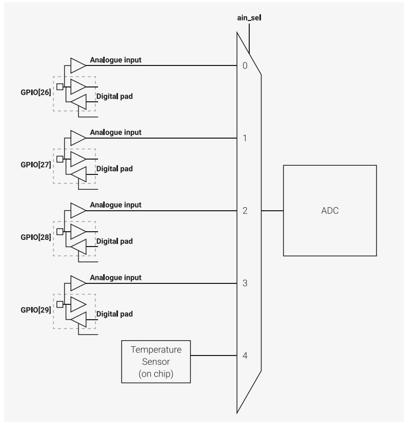
The diagram illustrates the ADC connection. On the left, four GPIO pins (GPIO[26], GPIO[27], GPIO[28], and GPIO[29]) are shown. Each pin has a dashed box containing an 'Analogue input' and a 'Digital pad'. The 'Analogue input' lines connect to a vertical bus labeled 'ain_sel' with values 0, 1, 2, and 3 respectively. A 'Temperature Sensor (on chip)' block connects to the 'ain_sel' bus at value 4. The 'ain_sel' bus then connects to the 'ADC' block on the right.
NOTE
When using an ADC input shared with a GPIO pin, the pin's digital functions must be disabled by setting IE low and OD high in the pin's pad control register. See Section 2.19.6.3, "Pad Control - User Bank" for details. The maximum ADC input voltage is determined by the digital IO supply voltage (IOVDD), not the ADC supply voltage (ADC_AVDD). For example, if IOVDD is powered at 1.8V, the voltage on the ADC inputs should not exceed 1.8V even if ADC_AVDD is powered at 3.3V. Voltages greater than IOVDD will result in leakage currents through the ESD protection diodes. See Section 5.5.3, "Pin Specifications" for details.
4.9.1. ADC controller
A digital controller manages the details of operating the RP2040 ADC, and provides additional functionality:
- • One-shot or free-running capture mode
- • Sample FIFO with DMA interface
- • Pacing timer (16 integer bits, 8 fractional bits) for setting free-running sample rate
- • Round-robin sampling of multiple channels in free-running capture mode
- • Optional right-shift to 8 bits in free-running capture mode, so samples can be DMA'd to a byte buffer in system memory
4.9.2. SAR ADC
The SAR ADC (Successive Approximation Register Analogue to Digital Converter) is a combination of digital controller, and analogue circuit as shown in Figure 115 .
Figure 115. SAR ADC Block diagram
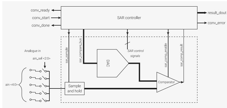
The ADC requires a 48MHz clock (
clk_adc
), which could come from the USB PLL. Capturing a sample takes 96 clock cycles (
\(
96 \times 1/48\text{MHz}
\)
) = 2µs per sample (500ksps). The clock must be set up correctly before enabling the ADC.
Once the ADC block is provided with a clock, and its reset has been removed, writing a 1 to
CS.EN
will start a short internal power-up sequence for the ADC's analogue hardware. After a few clock cycles,
CS.READY
will go high, indicating the ADC is ready to start its first conversion.
The ADC can be disabled again at any time by clearing
CS.EN
, to save power.
CS.EN
does
not
enable the temperature sensor bias source (see
Section 4.9.5
). This is controlled separately.
The ADC input is capacitive, and when sampling, it places about 1pF across the input (there will be additional capacitance from outside the ADC, such as packaging and PCB routing, to add to this). The effective impedance, even when sampling at 500ksps, is over 100kΩ, and for DC measurements there should be no need to buffer.
4.9.2.1. One-shot Sample
Writing a 1 to
CS.START_ONCE
will immediately start a new conversion.
CS.READY
will go low, to show that a conversion is currently in progress. After 96 cycles of
clk_adc
,
CS.READY
will go high. The 12-bit conversion result is available in
RESULT
.
The ADC input to be sampled is selected by writing to
CS.AINSEL
, any time before the conversion starts. An
AINSEL
value of 0...3 selects the ADC input on GPIO 26...29.
AINSEL
of 4 selects the internal temperature sensor.
i NOTE
No settling time is required when switching
AINSEL
.
4.9.2.2. Free-running Sampling
When
CS.START_MANY
is set, the ADC will automatically start new conversions at regular intervals. The most recent conversion result is always available in
RESULT
, but for IRQ or DMA driven streaming of samples, the ADC FIFO must be enabled (
Section 4.9.2.4
).
By default (
DIV = 0
), new conversions start immediately upon the previous conversion finishing, so a new sample is produced every 96 cycles. At a clock frequency of 48MHz, this produces 500ksps.
Setting
DIV.INT
to some positive value
\(
n
\)
will trigger the ADC once per
\(
n + 1
\)
cycles, though the ADC ignores this if a conversion is currently in progress, so generally
\(
n
\)
will be
\(
\geq 96
\)
. For example, setting
DIV.INT
to 47999 will run the ADC at 1ksps, if running from a 48MHz clock.
The pacing timer supports fractional-rate division (first order delta sigma). When setting
DIV.FRAC
to a nonzero value,
the ADC will start a new conversion once per \( 1 + \text{INT} + \frac{\text{FRAC}}{256} \) cycles on average, by changing the sample interval between \( \text{INT} + 1 \) and \( \text{INT} + 2 \) .
4.9.2.3. Sampling Multiple Inputs
CS.RROBIN allows the ADC to sample multiple inputs, in an interleaved fashion, while performing free-running sampling. Each bit in RROBIN corresponds to one of the five possible values of CS.AINSEL . When the ADC completes a conversion, CS.AINSEL will automatically cycle to the next input whose corresponding bit is set in RROBIN .
The round-robin sampling feature is disabled by writing all-zeroes to CS.RROBIN .
For example, if AINSEL is initially 0, and RROBIN is set to 0x06 (bits 1 and 2 are set), the ADC will sample channels in the following order:
- 1. Channel 0
- 2. Channel 1
- 3. Channel 2
- 4. Channel 1
- 5. Channel 2
- 6. Channel 1...
i NOTE
The initial value of AINSEL does not need to correspond with a set bit in RROBIN .
4.9.2.4. Sample FIFO
The ADC samples can be read directly from the RESULT register, or stored in a local 8-entry FIFO and read out from FIFO . FIFO operation is controlled by the FCS register.
If FCS.EN is set, the result of each ADC conversion is written to the FIFO. A software interrupt handler or the RP2040 DMA can read this sample from the FIFO when notified by the ADC's IRQ or DREQ signals. Alternatively, software can poll the status bits in FCS to wait for each sample to become available.
If the FIFO is full when a conversion completes, the sticky error flag FCS.OVER is set. The current FIFO contents are not changed by this event, but any conversion that completes whilst the FIFO is full will be lost.
There are two flags that control the data written to the FIFO by the ADC:
- • FCS.SHIFT will right-shift the FIFO data to eight bits in size (i.e. FIFO bits 7:0 are conversion result bits 11:4). This is suitable for 8-bit DMA transfer to a byte buffer in memory, allowing deeper capture buffers, at the cost of some precision.
- • FCS.ERR will set the FIFO.ERR flag of each FIFO value, showing that a conversion error took place, i.e. the SAR failed to converge (see below)
CAUTION
Conversion errors produce undefined results, and the corresponding sample should be discarded. They indicate that the comparison of one or more bits failed to complete in the time allowed. Normally this is caused by comparator metastability, i.e. the closer to the comparator threshold the input signal is, the longer it will take to make a decision. The high gain of the comparator reduces the probability that no decision is made.
4.9.2.5. DMA
The RP2040 DMA (Section 2.5) can fetch ADC samples from the sample FIFO, by performing a normal memory-mapped read on the FIFO register, paced by the ADC_DREQ system data request signal. The following must be considered:
- • The sample FIFO must be enabled (FCS.EN) so that samples are written to it; the FIFO is disabled by default so that it does not inadvertently fill when the ADC is used for one-shot conversions.
- • The ADC's data request handshake (DREQ) must be enabled, via FCS.DREQ_EN.
- • The DMA channel used for the transfer must select the DREQ_ADC data request signal (Section 2.5.3.1).
- • The threshold for DREQ assertion (FCS.THRESH) should be set to 1, so that the DMA transfers as soon as a single sample is present in the FIFO. Note this is also the threshold used for IRQ assertion, so non-DMA use cases might prefer a higher value for less frequent interrupts.
- • If the DMA transfer size is set to 8 bits, so that the DMA transfers to a byte array in memory, FCS.SHIFT must also be set, to pre-shift the FIFO samples to 8 bits of significance.
- • If multiple input channels are to be sampled, CS.RROBIN contains a 5-bit mask of those channels (4 external inputs plus temperature sensor). Additionally CS.AINSEL must select the channel for the first sample.
- • The ADC sample rate (Section 4.9.2.2) should be configured before starting the ADC.
Once the ADC is suitably configured, the DMA channel should be started first, and the ADC conversion should be started second, via CS.START_MANY. Once the DMA completes, the ADC can be halted, or a new DMA transfer promptly started. After clearing CS.START_MANY to halt the ADC, software should also poll CS.READY to make sure the last conversion has finished, and then drain any stray samples from the FIFO.
4.9.2.6. Interrupts
An interrupt can be generated when the FIFO level reaches a configurable threshold FCS.THRESH. The interrupt output must be enabled via INTE.
Status can be read from INTS. The interrupt is cleared by draining the FIFO to a level lower than FCS.THRESH.
4.9.2.7. Supply
The ADC supply is separated out on its own pin to allow noise filtering.
4.9.3. ADC ENOB
The ADC was characterised and the ENOB of the ADC was measured. Testing was carried out at room temperature across silicon lots, with tests being done on 3 typical (tt) as well as 3 fast (ff) and 3 slow (ss) corner RP2040 devices. The typical, minimum, and maximum values in Table 566 reflect the silicon used in the testing.
Table 565. Parameters used during the testing.
| Parameter | Value |
|---|---|
| Sample rate | 250ksps |
| Parameter | Value |
|---|---|
| FFT window | 5 term Blackman-Harris |
| FFT bins | 4,096 |
| FFT averaging | none |
| Input level min | 1 |
| Input level max | 4,094 |
| Input frequency | 997Hz |
It should be noted that THD is normally calculated using the first 5 or 6 harmonics. However as INL/DNL errors (see Section 4.9.4 ) create more than this, the first 30 peaks are used. This makes the THD value slightly worse, but more representative of reality.
Table 566. Results for various parts tested (fast, slow, and typical).
| Min | Typical | Max | |
|---|---|---|---|
| THD 1 | -55.6dB | 55dB | -54.4dB |
| SNR | 60.9dB | 61.5dB | 62.0dB |
| SFDR | 59.2dB | 59.9dB | 60.5dB |
| SINAD | 53.6dB | 54.0dB | 54.6dB |
| ENOB | 8.6 | 8.7 | 8.8 |
1 As the INL creates a large number of harmonics, the highest 30 peaks were used. This is different from conventional calculations of THD.
! IMPORTANT
Testing was carried out using a board with a low-noise on-board voltage reference as, when characterising the ADC, it is important that there are no other noise sources affecting the measurements.
4.9.4. INL and DNL
Integral Non-Linearity (INL) and Differential Non-Linearity (DNL) are used to measure the error of the quantisation of the incoming signal that the ADC generates. In an ideal ADC the input-to-output transfer function should have a linear quantised transfer between the analogue input signal and the digitised output signal. The RP2040 ADC INL values for each binary result are shown in Figure 116 , illustrating that the error is a sawtooth rather than the expected curve.
Figure 116. ATE machine results for INL (RP2040).
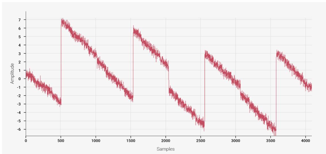
Nominally an ADC moves from one digital value to the next digital value, colloquially expressed as “no missing codes”. However, if the ADC skips a value bin this would cause a spike in the Differential Non-Linearity (DNL) error. These types of error often only occur at specific codes due to the design of the ADC.
The RP2040 ADC has a DNL which is mostly flat, and below 1 LSB. However at four values — 512, 1536, 2560, and 3,584 — the ADC’s DNL error peaks, see Figure 117
Figure 117. ATE machine results for DNL (RP2040).
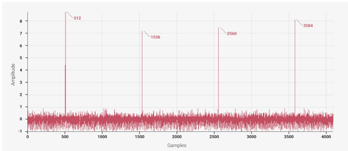
The INL and DNL errors come from an error in the scaling of some internal capacitors of the ADC. These capacitors are small in value (only tens of femto Farads) and at these very small values, chip simulation of these capacitors can deviate slightly from reality. If these capacitors had matched correctly, the ADCs performance could have been better.
These INL and DNL errors will somewhat limit the performance of the ADC dependent on use case (See Errata RP2040-E11 ).
4.9.5. Temperature Sensor
The temperature sensor measures the \( V_{be} \) voltage of a biased bipolar diode, connected to the fifth ADC channel (AINSEL=4). Typically, \( V_{be} = 0.706V \) at 27 degrees C, with a slope of \( -1.721mV \) per degree. Therefore the temperature can be approximated as follows:
As the \( V_{be} \) and the \( V_{be} \) slope can vary over the temperature range, and from device to device, some user calibration may be required if accurate measurements are required.
The temperature sensor’s bias source must be enabled before use, via CS.TS_EN . This increases current consumption on ADC_AVDD by approximately 40µA.
Image: Note icon
NOTEThe on board temperature sensor is very sensitive to errors in the reference voltage. If the ADC returns a value of 891 this would correspond to a temperature of 20.1°C. However if the reference voltage is 1% lower than 3.3V then the same reading of 891 would correspond to 24.3°C. You would see a change in temperature of over 4°C for a small 1% change in reference voltage. Therefore if you want to improve the accuracy of the internal temperature sensor it is worth considering adding an external reference voltage.
Image: Note icon
NOTEThe INL errors, see Section 4.9.4 , aren’t in the usable temperature range of the ADC.
4.9.6. List of Registers
The ADC registers start at a base address of
0x4004c000
(defined as
ADC_BASE
in SDK).
Table 567. List of ADC registers
| Offset | Name | Info |
|---|---|---|
| 0x00 | CS | ADC Control and Status |
| 0x04 | RESULT | Result of most recent ADC conversion |
| 0x08 | FCS | FIFO control and status |
| 0x0c | FIFO | Conversion result FIFO |
| 0x10 | DIV | Clock divider. If non-zero, CS_START_MANY will start conversions at regular intervals rather than back-to-back. The divider is reset when either of these fields are written. Total period is 1 + INT + FRAC / 256 |
| 0x14 | INTR | Raw Interrupts |
| 0x18 | INTE | Interrupt Enable |
| 0x1c | INTF | Interrupt Force |
| 0x20 | INTS | Interrupt status after masking & forcing |
ADC: CS Register
Offset: 0x00
Description
ADC Control and Status
Table 568. CS Register
| Bits | Description | Type | Reset |
|---|---|---|---|
| 31:21 | Reserved. | - | - |
| 20:16 | RROBIN
: Round-robin sampling. 1 bit per channel. Set all bits to 0 to disable. Otherwise, the ADC will cycle through each enabled channel in a round-robin fashion. The first channel to be sampled will be the one currently indicated by AINSEL. AINSEL will be updated after each conversion with the newly-selected channel. | RW | 0x00 |
| 15 | Reserved. | - | - |
| Bits | Description | Type | Reset |
|---|---|---|---|
| 14:12 | AINSEL : Select analog mux input. Updated automatically in round-robin mode. | RW | 0x0 |
| 11 | Reserved. | - | - |
| 10 | ERR_STICKY : Some past ADC conversion encountered an error. Write 1 to clear. | WC | 0x0 |
| 9 | ERR : The most recent ADC conversion encountered an error; result is undefined or noisy. | RO | 0x0 |
| 8 | READY
: 1 if the ADC is ready to start a new conversion. Implies any previous conversion has completed. 0 whilst conversion in progress. | RO | 0x0 |
| 7:4 | Reserved. | - | - |
| 3 | START_MANY : Continuously perform conversions whilst this bit is 1. A new conversion will start immediately after the previous finishes. | RW | 0x0 |
| 2 | START_ONCE : Start a single conversion. Self-clearing. Ignored if start_many is asserted. | SC | 0x0 |
| 1 | TS_EN : Power on temperature sensor. 1 - enabled. 0 - disabled. | RW | 0x0 |
| 0 | EN
: Power on ADC and enable its clock. 1 - enabled. 0 - disabled. | RW | 0x0 |
ADC: RESULT Register
Offset: 0x04
Table 569. RESULT Register
| Bits | Description | Type | Reset |
|---|---|---|---|
| 31:12 | Reserved. | - | - |
| 11:0 | Result of most recent ADC conversion | RO | 0x000 |
ADC: FCS Register
Offset: 0x08
Description
FIFO control and status
Table 570. FCS Register
| Bits | Description | Type | Reset |
|---|---|---|---|
| 31:28 | Reserved. | - | - |
| 27:24 | THRESH : DREQ/IRQ asserted when level >= threshold | RW | 0x0 |
| 23:20 | Reserved. | - | - |
| 19:16 | LEVEL : The number of conversion results currently waiting in the FIFO | RO | 0x0 |
| 15:12 | Reserved. | - | - |
| 11 | OVER : 1 if the FIFO has been overflowed. Write 1 to clear. | WC | 0x0 |
| 10 | UNDER : 1 if the FIFO has been underflowed. Write 1 to clear. | WC | 0x0 |
| 9 | FULL | RO | 0x0 |
| 8 | EMPTY | RO | 0x0 |
| 7:4 | Reserved. | - | - |
| Bits | Description | Type | Reset |
|---|---|---|---|
| 3 | DREQ_EN : If 1: assert DMA requests when FIFO contains data | RW | 0x0 |
| 2 | ERR : If 1: conversion error bit appears in the FIFO alongside the result | RW | 0x0 |
| 1 | SHIFT : If 1: FIFO results are right-shifted to be one byte in size. Enables DMA to byte buffers. | RW | 0x0 |
| 0 | EN : If 1: write result to the FIFO after each conversion. | RW | 0x0 |
ADC: FIFO Register
Offset: 0x0c
Description
Conversion result FIFO
Table 571. FIFO Register
| Bits | Description | Type | Reset |
|---|---|---|---|
| 31:16 | Reserved. | - | - |
| 15 | ERR : 1 if this particular sample experienced a conversion error. Remains in the same location if the sample is shifted. | RF | - |
| 14:12 | Reserved. | - | - |
| 11:0 | VAL | RF | - |
ADC: DIV Register
Offset: 0x10
Description
Clock divider. If non-zero, CS_START_MANY will start conversions at regular intervals rather than back-to-back.
The divider is reset when either of these fields are written.
Total period is \( 1 + \text{INT} + \text{FRAC} / 256 \)
Table 572. DIV Register
| Bits | Description | Type | Reset |
|---|---|---|---|
| 31:24 | Reserved. | - | - |
| 23:8 | INT : Integer part of clock divisor. | RW | 0x0000 |
| 7:0 | FRAC : Fractional part of clock divisor. First-order delta-sigma. | RW | 0x00 |
ADC: INTR Register
Offset: 0x14
Description
Raw Interrupts
Table 573. INTR Register
| Bits | Description | Type | Reset |
|---|---|---|---|
| 31:1 | Reserved. | - | - |
| 0 | FIFO:
Triggered when the sample FIFO reaches a certain level. This level can be programmed via the FCS_THRESH field. | RO | 0x0 |
ADC: INTE Register
Offset: 0x18
Description
Interrupt Enable
Table 574. INTE Register
| Bits | Description | Type | Reset |
|---|---|---|---|
| 31:1 | Reserved. | - | - |
| 0 | FIFO:
Triggered when the sample FIFO reaches a certain level. This level can be programmed via the FCS_THRESH field. | RW | 0x0 |
ADC: INTF Register
Offset: 0x1c
Description
Interrupt Force
Table 575. INTF Register
| Bits | Description | Type | Reset |
|---|---|---|---|
| 31:1 | Reserved. | - | - |
| 0 | FIFO:
Triggered when the sample FIFO reaches a certain level. This level can be programmed via the FCS_THRESH field. | RW | 0x0 |
ADC: INTS Register
Offset: 0x20
Description
Interrupt status after masking & forcing
Table 576. INTS Register
| Bits | Description | Type | Reset |
|---|---|---|---|
| 31:1 | Reserved. | - | - |
| 0 | FIFO:
Triggered when the sample FIFO reaches a certain level. This level can be programmed via the FCS_THRESH field. | RO | 0x0 |
4.10. SSI
Synopsys Documentation
Synopsys Proprietary. Used with permission.
RP2040 has a Synchronous Serial Interface (SSI) controller which appears on the QSPI pins and is used to communicate with external Flash devices. The SSI forms part of the XIP block.
The SSI controller is based on a configuration of the Synopsys DW_apb_ssi IP (v4.01a).
4.10.1. Overview
In order for the DW_apb_ssi to connect to a serial-master or serial-slave peripheral device, the peripheral must have a least one of the following interfaces:
Motorola Serial Peripheral Interface (SPI)
A four-wire, full-duplex serial protocol from Motorola. There are four possible combinations for the serial clock phase and polarity. The clock phase (SCPH) determines whether the serial transfer begins with the falling edge of the slave select signal or the first edge of the serial clock. The slave select line is held high when the DW_apb_ssi is idle or disabled.
Texas Instruments Serial Protocol (SSP)
A four-wire, full-duplex serial protocol. The slave select line used for SPI and Microwire protocols doubles as the frame indicator for the SSP protocol.
National Semiconductor Microwire
A half-duplex serial protocol, which uses a control word transmitted from the serial master to the target serial slave.
You can program the FRF (frame format) bit field in the Control Register 0 (CTRLR0) to select which protocol is used.
The serial protocols supported by the DW_apb_ssi allow for serial slaves to be selected or addressed using either hardware or software. When implemented in hardware, serial slaves are selected under the control of dedicated hardware select lines. The number of select lines generated from the serial master is equal to the number of serial slaves present on the bus. The serial-master device asserts the select line of the target serial slave before data transfer begins. This architecture is illustrated in Figure 118 .
When implemented in software, the input select line for all serial slave devices should originate from a single slave select output on the serial master. In this mode it is assumed that the serial master has only a single slave select output. If there are multiple serial masters in the system, the slave select output from all masters can be logically ANDed to generate a single slave select input for all serial slave devices. The main program in the software domain controls selection of the target slave device; this architecture is illustrated in Figure 118 . Software would use the SSIENR register in all slaves in order to control which slave is to respond to the serial transfer request from the master device.
The DW_apb_ssi does not enforce hardware or software control for serial-slave device selection. You can configure the DW_apb_ssi for either implementation, illustrated in Figure 118 .
Figure 118.
Hardware/Software
Slave Selection.
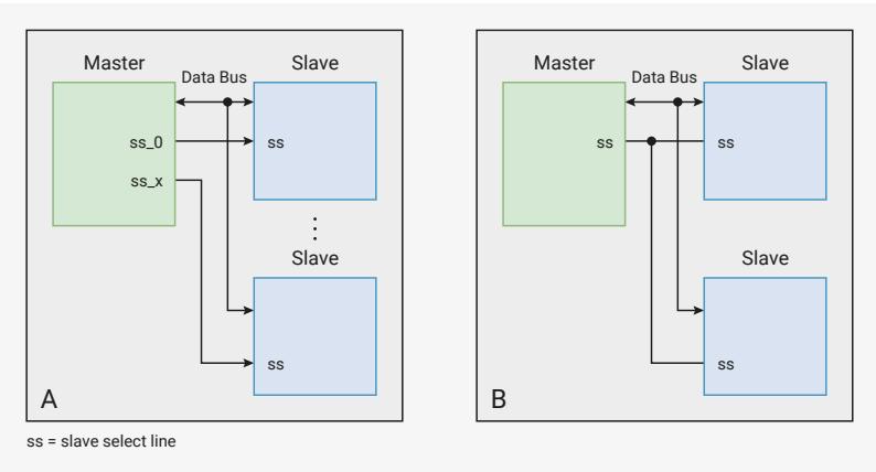
Diagram A (Hardware Selection): A Master block (green) has multiple slave select outputs labeled
ss_0
and
ss_x
. Each output connects to a corresponding slave select input labeled
ss
on a Slave block (blue). Multiple Slave blocks are shown, each with its own dedicated
ss
line from the Master. A shared Data Bus connects the Master to all Slaves.
Diagram B (Software Selection): A Master block (green) has a single slave select output labeled
ss
. This output connects to the slave select input labeled
ss
on all Slave blocks (blue). Multiple Slave blocks share the same
ss
line from the Master. A shared Data Bus connects the Master to all Slaves.
Legend:
ss
= slave select line
4.10.2. Features
The DW_apb_ssi is a configurable and programmable component that is a full-duplex master serial interface. The host processor accesses data, control, and status information on the DW_apb_ssi through the APB interface. The DW_apb_ssi also interfaces with the DMA Controller for bulk data transfer.
The DW_apb_ssi is configured as a serial master. The DW_apb_ssi can connect to any serial-slave peripheral device using one of the following interfaces:
- • Motorola Serial Peripheral Interface (SPI)
- • Texas Instruments Serial Protocol (SSP)
- • National Semiconductor Microwire
On RP2040, the DW_apb_ssi is a component of the flash execute-in-place subsystem (see Section 2.6.3 ), and provides communication with an external SPI, dual-SPI or quad-SPI flash device.
4.10.2.1. IO connections
The SSI controller connects to the following pins:
- • QSPI_SCLK Connected to output clock sclk_out
- • QSPI_SS_N Connected to chip select ss_o_n
- • QSPI_SD[3:0] Connected to data bus txd and rx
Some pins on the IP are tied off as not used:
- • ss_in_n is tied high
Clock connections are as follows:
- • pclk and sclk are driven from clk_sys
4.10.3. IP Modifications
The following modifications were made to the Synopsys DW_apb_ssi hardware:
- 1. XIP accesses are byte-swapped, such that the least-addressed byte is in the least-significant position
- 2. When SPI_CTRLR0_INST_L is 0, the XIP instruction field is appended to the end of the address for XIP accesses, rather than prepended to the beginning
- 3. The reset value of DMARDLR is increased from 0 to 4. The SSI to DMA handshaking on RP2040 requests only single transfers or bursts of four, depending on whether the RX FIFO level has reached DMARDLR , so DMARDLR should not be changed from this value.
The first of these changes allows mixed-size accesses by a little-endian busmaster, such as the RP2040 DMA, or the Cortex-M0+ configuration used on RP2040. Note that this only applies to XIP accesses (RP2040 system addresses in the range 0x10000000 to 0x13ffffff ), not to direct access to the DW_apb_ssi FIFOs. When accessing the SSI directly, it may be necessary for software to swap bytes manually, or to use the RP2040 DMA's byte swap feature.
The second supports issuing of continuation bits following the XIP address, so that command-prefix-free XIP modes can be supported (e.g. EBh Quad I/O Fast Read on Winbond devices), for greater performance. For example, the following configuration would be used to issue a standard 03h serial read command for each access to the XIP address window:
- • SPI_CTRLR0_INST_L = 8 bits
- • SPI_CTRLR0_ADDR_L = 24 bits
- • SPI_CTRLR0_XIP_CMD = 0x03
This will first issue eight command bits ( 0x03 ), then issue 24 address bits, then clock in the data bits. The configuration used for EBh quad read, after the flash has entered the XIP state, would be:
- • SPI_CTRLR0_INST_L = 0
- • SPI_CTRLR0_ADDR_L = 32 bits
- • SPI_CTRLR0_XIP_CMD = 0xa0 (continuation code on W25Qx devices)
For each XIP access, the DW_apb_ssi will issue 32 "address" bits, consisting of the 24 LSBs of the RP2040 system bus
address, followed by the 8-bit continuation code
0xa0
. No command prefix is issued.
4.10.3.1. Example of Target Slave Selection Using Software
The following example is pseudo code that illustrates how to use software to select the target slave.
1 int main() {
2     disable_all_serial_devices(); ①
3     initialize_mst(ssi_mst_1); ②
4     initialize_slv(ssi_slv_1); ③
5     start_serial_xfer(ssi_mst_1); ④
6 }
① This function sets the SSLEN bit to logic '0' in the SSIENR register of each device on the serial bus.
② This function initializes the master device for the serial transfer;
- 1. Write CTRLR0 to match the required transfer
- 2. If transfer is receive only write number of frames into CTRLR1
- 3. Write BAUDR to set the transfer baud rate.
- 4. Write TXFTLR and RXFTLR to set FIFO threshold levels
- 5. Write IMR register to set interrupt masks
- 6. Write SER register bit[0] to logic '1'
- 7. Write SSIENR register bit[0] to logic '1' to enable the master.
③ This function initializes the target slave device (slave 1 in this example) for the serial transfer;
- 1. Write CTRLR0 to match the required transfer
- 2. Write TXFTLR and RXFTLR to set FIFO threshold levels
- 3. Write IMR register to set interrupt masks
- 4. Write SSIENR register bit[0] to logic '1' to enable the slave.
- 5. If the slave is to transmit data, write data into TX FIFO. Now the slave is enabled and awaiting an active level on its ss_in_n input port. Note all other serial slaves are disabled (SSLEN=0) and therefore will not respond to an active level on their ss_in_n port.
④ This function begins the serial transfer by writing transmit data into the master's TX FIFO. User can poll the busy status with a function or use an ISR to determine when the serial transfer has completed.
4.10.4. Clock Ratios
The maximum frequency of the bit-rate clock (sclk_out) is one-half the frequency of ssi_clk. This allows the shift control logic to capture data on one clock edge of sclk_out and propagate data on the opposite edge.
Figure 119 illustrates the maximum ratio between sclk_out and ssi_clk.
Figure 119. Maximum \( sclk\_out/ssi\_clk \) Ratio.
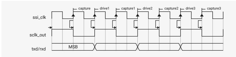
The \( sclk\_out \) line toggles only when an active transfer is in progress. At all other times it is held in an inactive state, as defined by the serial protocol under which it operates.
The frequency of \( sclk\_out \) can be derived from the following equation:
SCKDV is a bit field in the programmable register BAUDR, holding any even value in the range 0 to 65,534. If SCKDV is 0, then \( sclk\_out \) is disabled.
4.10.4.1. Frequency Ratio Summary
A summary of the frequency ratio restrictions between the bit-rate clock ( \( sclk\_out \) ) and the DW_apb_ssi peripheral clock ( \( ssi\_clk \) ) are as follows:
- • \( F_{ssi\_clk} \geq 2 \times (maximum F_{sclk\_out}) \)
4.10.5. Transmit and Receive FIFO Buffers
The FIFO buffers used by the DW_apb_ssi are internal D-type flip-flops that are 16 entries deep. The width of both transmit and receive FIFO buffers is fixed at 32 bits, due to the serial specifications, which state that a serial transfer (data frame) can be 4 to 16/32 bits in length. Data frames that are less than 32 bits must be right-justified when written into the transmit FIFO buffer. The shift control logic automatically right-justifies receive data in the receive FIFO buffer.
Each data entry in the FIFO buffers contains a single data frame. It is impossible to store multiple data frames in a single FIFO location; for example, you may not store two 8-bit data frames in a single FIFO location. If an 8-bit data frame is required, the upper bits of the FIFO entry are ignored or unused when the serial shifter transmits the data.
i NOTE
The transmit and receive FIFO buffers are cleared when the DW_apb_ssi is disabled (SSI_EN = 0) or when it is reset (presetrn).
The transmit FIFO is loaded by APB write commands to the DW_apb_ssi data register (DR). Data are popped (removed) from the transmit FIFO by the shift control logic into the transmit shift register. The transmit FIFO generates a FIFO empty interrupt request ( \( ssi\_txe\_intr \) ) when the number of entries in the FIFO is less than or equal to the FIFO threshold value. The threshold value, set through the programmable register TXFTLR, determines the level of FIFO entries at which an interrupt is generated. The threshold value allows you to provide early indication to the processor that the transmit FIFO is nearly empty. A transmit FIFO overflow interrupt ( \( ssi\_txo\_intr \) ) is generated if you attempt to write data into an already full transmit FIFO.
Data are popped from the receive FIFO by APB read commands to the DW_apb_ssi data register (DR). The receive FIFO is loaded from the receive shift register by the shift control logic. The receive FIFO generates a FIFO-full interrupt request ( \( ssi\_rxf\_intr \) ) when the number of entries in the FIFO is greater than or equal to the FIFO threshold value plus one. The threshold value, set through programmable register RXFTLR, determines the level of FIFO entries at which an interrupt is generated.
The threshold value allows you to provide early indication to the processor that the receive FIFO is nearly full. A receive FIFO overrun interrupt ( \( ssi\_rxo\_intr \) ) is generated when the receive shift logic attempts to load data into a completely full receive FIFO. However, this newly received data are lost. A receive FIFO underflow interrupt ( \( ssi\_rxu\_intr \) ) is generated if
you attempt to read from an empty receive FIFO. This alerts the processor that the read data are invalid.
Table 577 provides description for different Transmit FIFO Threshold values.
Table 577. Transmit
FIFO Threshold (TFT)
Decode Values
| TFT Value | Description |
|---|---|
| 0000_0000 | ssi_txe_intr is asserted when zero data entries are present in transmit FIFO |
| 0000_0001 | ssi_txe_intr is asserted when one or less data entry is present in transmit FIFO |
| 0000_0010 | ssi_txe_intr is asserted when two or less data entries are present in transmit FIFO |
| ... | ... |
| 0000_1101 | ssi_txe_intr is asserted when 13 or less data entries are present in transmit FIFO |
| 0000_1110 | ssi_txe_intr is asserted when 14 or less data entries are present in transmit FIFO |
| 0000_1111 | ssi_txe_intr is asserted when 15 or less data entries are present in transmit FIFO |
Table 578 provides description for different Receive FIFO Threshold values.
Table 578. Receive
FIFO Threshold (RFT)
Decode Values
| RFT Value | Description |
|---|---|
| 0000_0000 | ssi_rxf_intr is asserted when one or more data entry is present in receive FIFO |
| 0000_0001 | ssi_rxf_intr is asserted when two or more data entries are present in receive FIFO |
| 0000_0010 | ssi_rxf_intr is asserted when three or more data entries are present in receive FIFO |
| ... | ... |
| 0000_1101 | ssi_rxf_intr is asserted when 14 or more data entries are present in receive FIFO |
| 0000_1110 | ssi_rxf_intr is asserted when 15 or more data entries are present in receive FIFO |
| 0000_1111 | ssi_rxf_intr is asserted when 16 data entries are present in receive FIFO |
4.10.6. 32-Bit Frame Size Support
The IP is configured to set the maximum programmable value in of data frame size to 32 bits. As a result the following features exist:
- • dfs_32 (CTRLR0[20:16]) are valid, which contains the value of data frame size. The new register field holds the values 0 to 31. The dfs (CTRLR0[3:0]) is invalid and writing to this register has no effect.
- • The receive and transmit FIFO widths are 32 bits.
- • All 32 bits of the data register are valid.
4.10.7. SSI Interrupts
The DW_apb_ssi supports combined and individual interrupt requests, each of which can be masked. The combined interrupt request is the ORed result of all other DW_apb_ssi interrupts after masking. Only the combined interrupt request is routed to the Interrupt Controller. All DW_apb_ssi interrupts are level interrupts and are active high.
The DW_apb_ssi interrupts are described as follows:
Transmit FIFO Empty Interrupt (ssi_txe_intr)
Set when the transmit FIFO is equal to or below its threshold value and requires service to prevent an under-run. The threshold value, set through a software-programmable register, determines the level of transmit FIFO entries at which an interrupt is generated. This interrupt is cleared by hardware when data are written into the transmit FIFO buffer, bringing it over the threshold level.
Transmit FIFO Overflow Interrupt (ssi_txo_intr)Set when an APB access attempts to write into the transmit FIFO after it has been completely filled. When set, data written from the APB is discarded. This interrupt remains set until you read the transmit FIFO overflow interrupt clear register (TXOICR).
Receive FIFO Full Interrupt (ssi_rxf_intr)Set when the receive FIFO is equal to or above its threshold value plus 1 and requires service to prevent an overflow. The threshold value, set through a software-programmable register, determines the level of receive FIFO entries at which an interrupt is generated. This interrupt is cleared by hardware when data are read from the receive FIFO buffer, bringing it below the threshold level.
Receive FIFO Overflow Interrupt (ssi_rxo_intr)Set when the receive logic attempts to place data into the receive FIFO after it has been completely filled. When set, newly received data are discarded. This interrupt remains set until you read the receive FIFO overflow interrupt clear register (RXOICR).
Receive FIFO Underflow Interrupt (ssi_rxu_intr)Set when an APB access attempts to read from the receive FIFO when it is empty. When set, 0s are read back from the receive FIFO. This interrupt remains set until you read the receive FIFO underflow interrupt clear register (RXUICR).
Multi-Master Contention Interrupt (ssi_mst_intr)Present only when the DW_apb_ssi component is configured as a serial-master device. The interrupt is set when another serial master on the serial bus selects the DW_apb_ssi master as a serial-slave device and is actively transferring data. This informs the processor of possible contention on the serial bus. This interrupt remains set until you read the multi-master interrupt clear register (MSTICR).
Combined Interrupt Request (ssi_intr)OR'ed result of all the above interrupt requests after masking. To mask this interrupt signal, you must mask all other DW_apb_ssi interrupt requests.
4.10.8. Transfer Modes
When transferring data on the serial bus, the DW_apb_ssi operates in the modes discussed in this section. The transfer mode (TMOD) is set by writing to control register 0 (CTRLR0).
i NOTE
The transfer mode setting does not affect the duplex of the serial transfer. TMOD is ignored for Microwire transfers, which are controlled by the MWCR register.
4.10.8.1. Transmit and Receive
When TMOD = 00b, both transmit and receive logic are valid. The data transfer occurs as normal according to the selected frame format (serial protocol). Transmit data are popped from the transmit FIFO and sent through the txd line to the target device, which replies with data on the rxd line. The receive data from the target device is moved from the receive shift register into the receive FIFO at the end of each data frame.
4.10.8.2. Transmit Only
When TMOD = 01b, the receive data are invalid and should not be stored in the receive FIFO. The data transfer occurs as normal, according to the selected frame format (serial protocol). Transmit data are popped from the transmit FIFO and sent through the txd line to the target device, which replies with data on the rxd line. At the end of the data frame, the receive shift register does not load its newly received data into the receive FIFO. The data in the receive shift register is
overwritten by the next transfer. You should mask interrupts originating from the receive logic when this mode is entered.
4.10.8.3. Receive Only
When
TMOD = 10b
, the transmit data are invalid. When configured as a slave, the transmit FIFO is never popped in Receive Only mode. The
txd
output remains at a constant logic level during the transmission. The data transfer occurs as normal according to the selected frame format (serial protocol). The receive data from the target device is moved from the receive shift register into the receive FIFO at the end of each data frame. You should mask interrupts originating from the transmit logic when this mode is entered.
4.10.8.4. EEPROM Read
i NOTE
This transfer mode is only valid for master configurations.
When
TMOD = 11b
, the transmit data is used to transmit an opcode and/or an address to the EEPROM device. Typically this takes three data frames (8-bit opcode followed by 8-bit upper address and 8-bit lower address). During the transmission of the opcode and address, no data is captured by the receive logic (as long as the
DW_apb_ssi
master is transmitting data on its
txd
line, data on the
rx
line is ignored). The
DW_apb_ssi
master continues to transmit data until the transmit FIFO is empty. Therefore, you should ONLY have enough data frames in the transmit FIFO to supply the opcode and address to the EEPROM. If more data frames are in the transmit FIFO than are needed, then read data is lost.
When the transmit FIFO becomes empty (all control information has been sent), data on the receive line (
rx
) is valid and is stored in the receive FIFO; the
txd
output is held at a constant logic level. The serial transfer continues until the number of data frames received by the
DW_apb_ssi
master matches the value of the
NDF
field in the
CTRLR1
register + 1.
i NOTE
EEPROM read mode is not supported when the
DW_apb_ssi
is configured to be in the SSP mode.
4.10.9. Operation Modes
The
DW_apb_ssi
can be configured in the fundamental modes of operation discussed in this section.
4.10.9.1. Serial Master Mode
This mode enables serial communication with serial-slave peripheral devices. When configured as a serial-master device, the
DW_apb_ssi
initiates and controls all serial transfers.
Figure 120
shows an example of the
DW_apb_ssi
configured as a serial master with all other devices on the serial bus configured as serial slaves.
Figure 120.
DW_apb_ssi
Configured as Master
Device
![Figure 120: DW_apb_ssi Master 1 connected to Slave Peripheral 1 and Slave Peripheral n. The diagram shows the internal signals of the master (txd, ssi_oe_n, rxd, sclk_out, ss_n[0], ss_n[1], ss_in_n) and how they are connected to the slave peripherals (DI, DO, SCLK, SS). A Glue Logic block is shown between the master and the slaves. A note states: 'Should be driven to inactive level (protocol-dependent) in single master systems; may not need glue logic'.](/RP2040/c742b650efac1e133860d9d0ee4a8d7d_img.jpg)
Should be driven to inactive level
(protocol-dependent) in single master
systems; may not need glue logic
The serial bit-rate clock, generated and controlled by the DW_apb_ssi, is driven out on the sclk_out line. When the DW_apb_ssi is disabled (SSI_EN = 0), no serial transfers can occur and sclk_out is held in “inactive” state, as defined by the serial protocol under which it operates.
Multiple master configuration is not supported.
4.10.9.1.1. RXD Sample Delay
When the DW_apb_ssi is configured as a master, additional logic can be included in the design in order to delay the default sample time of the rxd signal. This additional logic can help to increase the maximum achievable frequency on the serial bus.
Round trip routing delays on the sclk_out signal from the master and the rxd signal from the slave can mean that the timing of the rxd signal—as seen by the master—has moved away from the normal sampling time. Figure 121 illustrates this situation.
Figure 121. Effects of
Round-Trip Routing
Delays on sclk_out
Signal
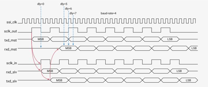
baud-rate=4
The Slave uses the sclk_out signal from the master as a strobe in order to drive rxd signal data onto the serial bus. Routing and sampling delays on the sclk_out signal by the slave device can mean that the rxd bit has not stabilized to the correct value before the master samples the rxd signal. Figure 121 shows an example of how a routing delay on the rxd signal can result in an incorrect rxd value at the default time when the master samples the port.
Without the RXD Sample Delay logic, the user would have to increase the baud-rate for the transfer in order to ensure that the setup times on the rxd signal are within range; this results in reducing the frequency of the serial interface.
When the RXD Sample Delay logic is included, the user can dynamically program a delay value in order to move the sampling time of the rxd signal equal to a number of ssi_clk cycles from the default.
The sample delay logic has a resolution of one ssi_clk cycle. Software can “train” the serial bus by coding a loop that continually reads from the slave and increments the master’s RXD Sample Delay value until the correct data is received by the master.
4.10.9.1.2. Data Transfers
Data transfers are started by the serial-master device. When the DW_apb_ssi is enabled (SSI_EN=1), at least one valid data entry is present in the transmit FIFO and a serial-slave device is selected. When actively transferring data, the busy flag (BUSY) in the status register (SR) is set. You must wait until the busy flag is cleared before attempting a new serial transfer.
i NOTE
The BUSY status is not set when the data are written into the transmit FIFO. This bit gets set only when the target slave has been selected and the transfer is underway. After writing data into the transmit FIFO, the shift logic does not begin the serial transfer until a positive edge of the sclk_out signal is present. The delay in waiting for this positive edge depends on the baud rate of the serial transfer. Before polling the BUSY status, you should first poll the TFE status (waiting for 1) or wait for \( BAUDR * ssi\_clk \) clock cycles.
4.10.9.1.3. Master SPI and SSP Serial Transfers
When the transfer mode is “transmit and receive” or “transmit only” (TMOD = 00b or TMOD = 01b, respectively), transfers are terminated by the shift control logic when the transmit FIFO is empty. For continuous data transfers, you must ensure that the transmit FIFO buffer does not become empty before all the data have been transmitted. The transmit FIFO threshold level (TXFTLR) can be used to early interrupt (ssi_txe_intr) the processor indicating that the transmit FIFO buffer is nearly empty. When a DMA is used for APB accesses, the transmit data level (DMATDLR) can be used to early request (dma_tx_req) the DMA Controller, indicating that the transmit FIFO is nearly empty. The FIFO can then be refilled with data to continue the serial transfer. The user may also write a block of data (at least two FIFO entries) into the transmit FIFO before enabling a serial slave. This ensures that serial transmission does not begin until the number of data-frames that make up the continuous transfer are present in the transmit FIFO.
When the transfer mode is “receive only” (TMOD = 10b), a serial transfer is started by writing one “dummy” data word into the transmit FIFO when a serial slave is selected. The txd output from the DW_apb_ssi is held at a constant logic level for the duration of the serial transfer. The transmit FIFO is popped only once at the beginning and may remain empty for the duration of the serial transfer. The end of the serial transfer is controlled by the “number of data frames” (NDF) field in control register 1 (CTRLR1).
If, for example, you want to receive 24 data frames from a serial-slave peripheral, you should program the NDF field with the value 23; the receive logic terminates the serial transfer when the number of frames received is equal to the NDF value + 1. This transfer mode increases the bandwidth of the APB bus as the transmit FIFO never needs to be serviced during the transfer. The receive FIFO buffer should be read each time the receive FIFO generates a FIFO full interrupt request to prevent an overflow.
When the transfer mode is “eeprom_read” (TMOD = 11b), a serial transfer is started by writing the opcode and/or address into the transmit FIFO when a serial slave (EEPROM) is selected. The opcode and address are transmitted to the EEPROM device, after which read data is received from the EEPROM device and stored in the receive FIFO. The end of the serial transfer is controlled by the NDF field in the control register 1 (CTRLR1).
NOTEEEPROM read mode is not supported when the DW_apb_ssi is configured to be in the SSP mode.
The receive FIFO threshold level (RXFTLR) can be used to give early indication that the receive FIFO is nearly full. When a DMA is used for APB accesses, the receive data level (DMARDLR) can be used to early request (dma_rx_req) the DMA Controller, indicating that the receive FIFO is nearly full.
A typical software flow for completing an SPI or SSP serial transfer from the DW_apb_ssi serial master is outlined as follows:
- 1. If the DW_apb_ssi is enabled, disable it by writing 0 to the SSI Enable register (SSIENR).
- 2. Set up the DW_apb_ssi control registers for the transfer; these registers can be set in any order.
- ◦ Write Control Register 0 (CTRLR0). For SPI transfers, the serial clock polarity and serial clock phase parameters must be set identical to target slave device.
- ◦ If the transfer mode is receive only, write CTRLR1 (Control Register 1) with the number of frames in the transfer minus 1; for example, if you want to receive four data frames, if you want to receive four data frames, write '3' into CTRLR1.
- ◦ Write the Baud Rate Select Register (BAUDR) to set the baud rate for the transfer.
- ◦ Write the Transmit and Receive FIFO Threshold Level registers (TXFTLR and RXFTLR, respectively) to set FIFO threshold levels.
- ◦ Write the IMR register to set up interrupt masks.
- ◦ The Slave Enable Register (SER) register can be written here to enable the target slave for selection. If a slave is enabled here, the transfer begins as soon as one valid data entry is present in the transmit FIFO. If no slaves are enabled prior to writing to the Data Register (DR), the transfer does not begin until a slave is enabled.
- 3. Enable the DW_apb_ssi by writing 1 to the SSIENR register.
- 4. Write data for transmission to the target slave into the transmit FIFO (write DR). If no slaves were enabled in the SER register at this point, enable it now to begin the transfer.
- 5. Poll the BUSY status to wait for completion of the transfer. The BUSY status cannot be polled immediately.
- 6. If a transmit FIFO empty interrupt request is made, write the transmit FIFO (write DR). If a receive FIFO full interrupt request is made, read the receive FIFO (read DR).
- 7. The transfer is stopped by the shift control logic when the transmit FIFO is empty. If the transfer mode is receive only (TMOD = 10b), the transfer is stopped by the shift control logic when the specified number of frames have been received. When the transfer is done, the BUSY status is reset to 0.
- 8. If the transfer mode is not transmit only (TMOD != 01b), read the receive FIFO until it is empty.
- 9. Disable the DW_apb_ssi by writing 0 to SSIENR.
Figure 122 shows a typical software flow for starting a DW_apb_ssi master SPI/SSP serial transfer. The diagram also shows the hardware flow inside the serial-master component.
Figure 122.
DW_apb_ssi Master
SPI/SSP Transfer Flow
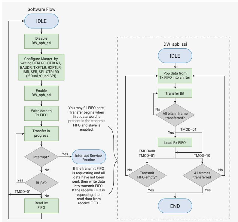
graph TD
    subgraph Software_Flow [Software Flow]
        IDLE1([IDLE]) --> Disable[Disable DW_apb_ssi]
        Disable --> Configure[Configure Master by writing CTRLR0, CTRLR1, BAUDR, TXFTLR, RXFTLR, IMR, SER, SPL, CTRLR0 (if Dual /Quad SPI)]
        Configure --> Enable[Enable DW_apb_ssi]
        Enable --> Write[Write data to Tx FIFO]
        Write --> Transfer[Transfer in progress]
        Transfer --> Interrupt{Interrupt?}
        Interrupt -- Yes --> ISR([Interrupt Service Routine])
        ISR --> Transfer
        Interrupt -- No --> Busy{BUSY?}
        Busy -- Yes --> Read[Read Rx FIFO]
        Read --> Transfer
        Busy -- No --> TMOD01[TMOD=01]
        TMOD01 --> Interrupt
    end

    subgraph DW_apb_ssi_Hardware_Flow [DW_apb_ssi]
        IDLE2([IDLE]) --> Pop[Pop data from Tx FIFO into shifter]
        Pop --> TransferBit[Transfer Bit]
        TransferBit --> AllBits{All bits in frame transferred?}
        AllBits -- No --> TransferBit
        AllBits -- Yes --> TMOD{TMOD}
        TMOD -- TMOD=01 --> LoadRx[Load Rx FIFO]
        LoadRx --> AllFrames{All frames transferred?}
        TMOD -- TMOD=00 --> TxEmpty{Transmit FIFO empty?}
        TMOD -- TMOD=10 --> TxEmpty
        AllFrames -- Yes --> END([END])
        TxEmpty -- Yes --> END
        TxEmpty -- No --> AllFrames
        AllFrames -- No --> LoadRx
    end

    Note[You may fill FIFO here: Transfer begins when first data word is present in the transmit FIFO and slave is enabled.]
    Note --- Transfer
    Note --- Read
4.10.9.1.4. Master Microwire Serial Transfers
Microwire serial transfers from the DW_apb_ssi serial master are controlled by the Microwire Control Register (MWCR). The MWHS bit field enables and disables the Microwire handshaking interface. The MDD bit field controls the direction of the data frame (the control frame is always transmitted by the master and received by the slave). The MWMOD bit field defines whether the transfer is sequential or nonsequential.
All Microwire transfers are started by the DW_apb_ssi serial master when there is at least one control word in the transmit FIFO and a slave is enabled. When the DW_apb_ssi master transmits the data frame (MDD = 1), the transfer is terminated by the shift logic when the transmit FIFO is empty. When the DW_apb_ssi master receives the data frame (MDD = 0), the termination of the transfer depends on the setting of the MWMOD bit field. If the transfer is nonsequential (MWMOD = 0), it is terminated when the transmit FIFO is empty after shifting in the data frame from the slave. When the transfer is sequential (MWMOD = 1), it is terminated by the shift logic when the number of data frames received is equal to the value in the CTRLR1 register + 1.
When the handshaking interface on the DW_apb_ssi master is enabled (MWHS = 1), the status of the target slave is polled after transmission. Only when the slave reports a ready status does the DW_apb_ssi master complete the transfer and clear its BUSY status. If the transfer is continuous, the next control/data frame is not sent until the slave device returns a ready status.
A typical software flow for completing a Microwire serial transfer from the DW_apb_ssi serial master is outlined as follows:
- 1. If the DW_apb_ssi is enabled, disable it by writing 0 to SSIENR.
- 2. Set up the DW_apb_ssi control registers for the transfer. These registers can be set in any order. Write CTRLR0 to set transfer parameters.
- ◦ If the transfer is sequential and the DW_apb_ssi master receives data, write CTRLR1 with the number of frames in the transfer minus 1; for instance, if you want to receive four data frames, write '3' into CTRLR1.
- ◦ Write BAUDR to set the baud rate for the transfer.
- ◦ Write TXFTLR and RXFTLR to set FIFO threshold levels.
- ◦ Write the IMR register to set up interrupt masks.
You can write the SER register to enable the target slave for selection. If a slave is enabled here, the transfer begins as soon as one valid data entry is present in the transmit FIFO. If no slaves are enabled prior to writing to the DR register, the transfer does not begin until a slave is enabled.
- 3. Enable the DW_apb_ssi by writing 1 to the SSIENR register.
- 4. If the DW_apb_ssi master transmits data, write the control and data words into the transmit FIFO (write DR). If the DW_apb_ssi master receives data, write the control word(s) into the transmit FIFO.
If no slaves were enabled in the SER register at this point, enable now to begin the transfer.
- 5. Poll the BUSY status to wait for completion of the transfer. The BUSY status cannot be polled immediately.
- 6. The transfer is stopped by the shift control logic when the transmit FIFO is empty. If the transfer mode is sequential and the DW_apb_ssi master receives data, the transfer is stopped by the shift control logic when the specified number of data frames is received. When the transfer is done, the BUSY status is reset to 0.
- 7. If the DW_apb_ssi master receives data, read the receive FIFO until it is empty.
- 8. Disable the DW_apb_ssi by writing 0 to SSIENR.
Figure 123 shows a typical software flow for starting a DW_apb_ssi master Microwire serial transfer. The diagram also shows the hardware flow inside the serial-master component.
Figure 123.
DW_apb_ssi Master
Microwire Transfer
Flow
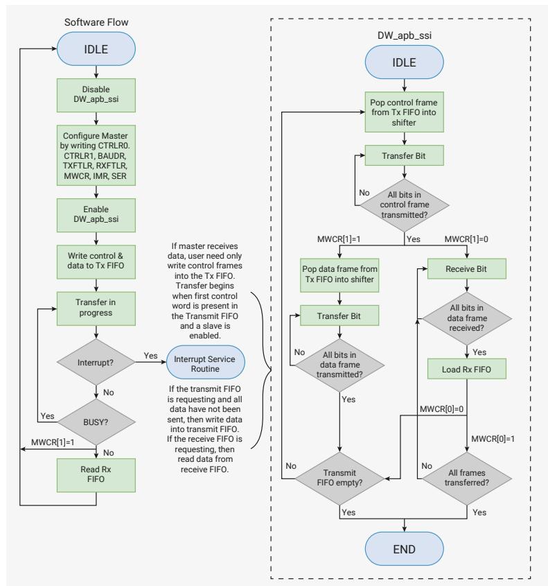
graph TD
    subgraph Software_Flow [Software Flow]
        IDLE1([IDLE]) --> Disable[Disable DW_apb_ssi]
        Disable --> Configure[Configure Master by writing CTRLR0, CTRLR1, BAUDR, TXFTLR, RXFTLR, MWCR, IMR, SER]
        Configure --> Enable[Enable DW_apb_ssi]
        Enable --> Write[Write control & data to Tx FIFO]
        Write --> Transfer[Transfer in progress]
        Transfer --> Interrupt{Interrupt?}
        Interrupt -- Yes --> ISR([Interrupt Service Routine])
        Interrupt -- No --> Busy{BUSY?}
        Busy -- Yes --> Read[Read Rx FIFO]
        Read --> Transfer
        Busy -- No --> MWCR1[MWCR[1]=1]
        MWCR1 --> Transfer
    end

    subgraph Hardware_Flow [DW_apb_ssi]
        IDLE2([IDLE]) --> PopCtrl[Pop control frame from Tx FIFO into shifter]
        PopCtrl --> TransferBit1[Transfer Bit]
        TransferBit1 --> AllBitsCtrl{All bits in control frame transmitted?}
        AllBitsCtrl -- No --> TransferBit1
        AllBitsCtrl -- Yes --> MWCR1_1[MWCR[1]=1]
        MWCR1_1 --> PopData[Pop data frame from Tx FIFO into shifter]
        PopData --> TransferBit2[Transfer Bit]
        TransferBit2 --> AllBitsData{All bits in data frame transmitted?}
        AllBitsData -- No --> TransferBit2
        AllBitsData -- Yes --> TransmitEmpty{Transmit FIFO empty?}
        TransmitEmpty -- Yes --> END([END])
        TransmitEmpty -- No --> TransferBit2
        MWCR1_1 --> ReceiveBit[Receive Bit]
        ReceiveBit --> AllBitsRx{All bits in data frame received?}
        AllBitsRx -- Yes --> LoadRx[Load Rx FIFO]
        LoadRx --> MWCR0_0[MWCR[0]=0]
        MWCR0_0 --> MWCR0_1[MWCR[0]=1]
        MWCR0_1 --> AllFrames{All frames transferred?}
        AllFrames -- Yes --> END
        AllFrames -- No --> ReceiveBit
    end

    ISR --> IDLE1
    Read --> IDLE1
    END --> IDLE1
Software Flow:
- IDLE
- Disable DW_apb_ssi
- Configure Master by writing CTRLR0, CTRLR1, BAUDR, TXFTLR, RXFTLR, MWCR, IMR, SER
- Enable DW_apb_ssi
- Write control & data to Tx FIFO
- Transfer in progress
- Interrupt?
- Interrupt Service Routine (if Interrupt is Yes)
- BUSY?
- Read Rx FIFO (if BUSY is Yes)
- MWCR[1]=1
Hardware Flow (DW_apb_ssi):
- IDLE
- Pop control frame from Tx FIFO into shifter
- Transfer Bit
- All bits in control frame transmitted?
- MWCR[1]=1
- Pop data frame from Tx FIFO into shifter
- Transfer Bit
- All bits in data frame transmitted?
- Transmit FIFO empty?
- END
- Receive Bit
- All bits in data frame received?
- Load Rx FIFO
- MWCR[0]=0
- MWCR[0]=1
- All frames transferred?
- END
Annotations:
- If master receives data, user need only write control frames into the Tx FIFO. Transfer begins when first control word is present in the Transmit FIFO and a slave is enabled.
- If the transmit FIFO is requesting and all data have not been sent, then write data into transmit FIFO.
- If the receive FIFO is requesting, then read data from receive FIFO.
4.10.10. Partner Connection Interfaces
The DW_apb_ssi can connect to any serial-slave peripheral device using one of the interfaces discussed in the following sections.
4.10.10.1. Motorola Serial Peripheral Interface (SPI)
With the SPI, the clock polarity (SCPOL) configuration parameter determines whether the inactive state of the serial clock is high or low. To transmit data, both SPI peripherals must have identical serial clock phase (SCPH) and clock polarity (SCPOL) values. The data frame can be 4 to 16/32 bits (depending upon SSI_MAX_XFER_SIZE) in length.
When the configuration parameter SCPH = 0, data transmission begins on the falling edge of the slave select signal. The first data bit is captured by the master and slave peripherals on the first edge of the serial clock; therefore, valid data must be present on the txd and rxd lines prior to the first serial clock edge.
Figure 124 shows a timing diagram for a single SPI data transfer with SCPH = 0. The serial clock is shown for configuration parameters SCPOL = 0 and SCPOL = 1.
Figure 124. SPI Serial Format (SCPH = 0)
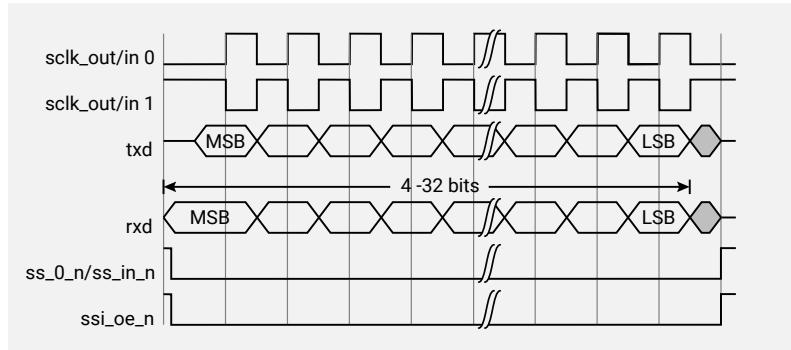
The following signals are illustrated in the timing diagrams in this section:
sclk_out
serial clock from DW_apb_ssi master
ss_0_n
slave select signal from DW_apb_ssi master
ss_in_n
slave select input to the DW_apb_ssi slave
ss_oe_n
output enable for the DW_apb_ssi master
txd
transmit data line for the DW_apb_ssi master
rxn
receive data line for the DW_apb_ssi master
Continuous data transfers are supported when SCPH = 0:
- When CTRLR0.SSTE is set to 1, the DW_apb_ssi toggles the slave select signal between frames and the serial clock is held to its default value while the slave select signal is active; this operating mode is illustrated in Figure 125.
Figure 125. Serial Format Continuous Transfers (SCPH = 0)
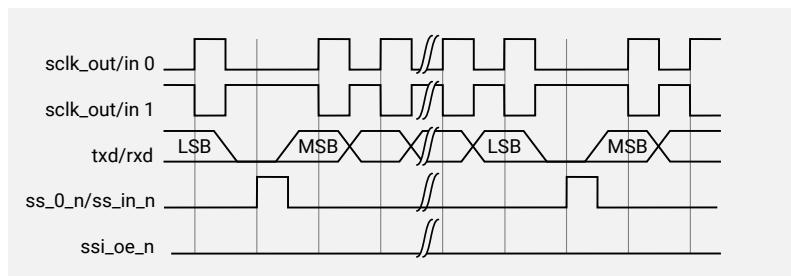
When the configuration parameter SCPH = 1, master peripherals begin transmitting data on the first serial clock edge
after the slave select line is activated. The first data bit is captured on the second (trailing) serial clock edge. Data are propagated by the master peripherals on the leading edge of the serial clock. During continuous data frame transfers, the slave select line may be held active-low until the last bit of the last frame has been captured.
Figure 126 shows the timing diagram for the SPI format when the configuration parameter SCPH = 1.
Figure 126. SPI Serial Format (SCPH = 1)
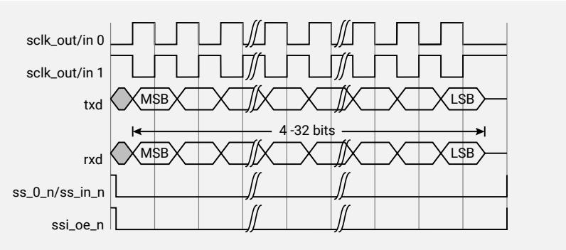
Continuous data frames are transferred in the same way as single frames, with the MSB of the next frame following directly after the LSB of the current frame. The slave select signal is held active for the duration of the transfer.
Figure 127 shows the timing diagram for continuous SPI transfers when the configuration parameter SCPH = 1.
Figure 127. SPI Serial Format Continuous Transfer (SCPH = 1)
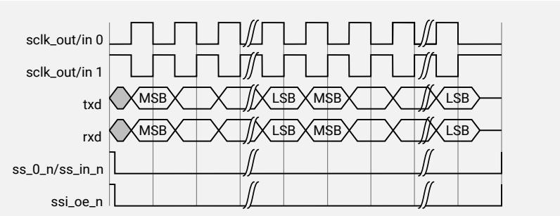
There are four possible transfer modes on the DW_apb_ssi for performing SPI serial transactions. For transmit and receive transfers (transfer mode field (9:8) of the Control Register 0 = 00b), data transmitted from the DW_apb_ssi to the external serial device is written into the transmit FIFO. Data received from the external serial device into the DW_apb_ssi is pushed into the receive FIFO.
Figure 128 shows the FIFO levels prior to the beginning of a serial transfer and the FIFO levels on completion of the transfer. In this example, two data words are transmitted from the DW_apb_ssi to the external serial device in a continuous transfer. The external serial device also responds with two data words for the DW_apb_ssi.
Figure 128. FIFO Status for Transmit & Receive SPI and SSP Transfers
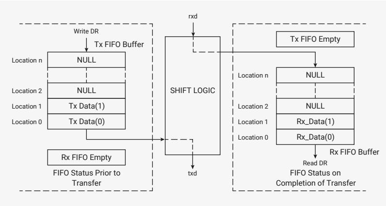
For transmit only transfers (transfer mode field (9:8) of the Control Register 0 = 01b), data transmitted from the DW_apb_ssi to the external serial device is written into the transmit FIFO. As the data received from the external serial device is deemed invalid, it is not stored in the DW_apb_ssi receive FIFO.
Figure 129 shows the FIFO levels prior to the beginning of a serial transfer and the FIFO levels on completion of the transfer. In this example, two data words are transmitted from the DW_apb_ssi to the external serial device in a continuous transfer.
Figure 129. FIFO Status for Transmit Only SPI and SSP Transfers
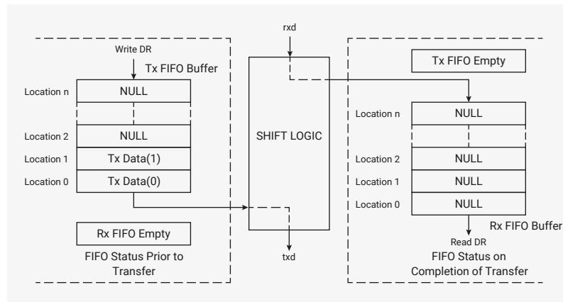
The diagram illustrates the FIFO status for transmit-only SPI and SSP transfers. It is divided into two main sections: 'FIFO Status Prior to Transfer' and 'FIFO Status on Completion of Transfer', separated by a dashed line.
FIFO Status Prior to Transfer:
- Tx FIFO Buffer: A vertical stack of four locations. Location 0 contains 'Tx Data(0)', Location 1 contains 'Tx Data(1)', and Locations 2 and n are 'NULL'. An arrow labeled 'Write DR' points to the top of this buffer.
- Rx FIFO Buffer: A single box labeled 'Rx FIFO Empty'.
- SHIFT LOGIC: A central block with 'rxd' input and 'txd' output.
FIFO Status on Completion of Transfer:
- Tx FIFO Buffer: All four locations (0, 1, 2, n) are now 'NULL'. An arrow labeled 'Tx FIFO Empty' points to the top of this buffer.
- Rx FIFO Buffer: A single box labeled 'Rx FIFO Empty'.
- SHIFT LOGIC: The same central block with 'rxd' input and 'txd' output.
Arrows indicate the flow of data from the Tx FIFO Buffer to the SHIFT LOGIC and from the SHIFT LOGIC to the Rx FIFO Buffer.
For receive only transfers (transfer mode field (9:8) of the Control Register 0 = 10b), data transmitted from the DW_apb_ssi to the external serial device is invalid, so a single dummy word is written into the transmit FIFO to begin the serial transfer. The txd output from the DW_apb_ssi is held at a constant logic level for the duration of the serial transfer. Data received from the external serial device into the DW_apb_ssi is pushed into the receive FIFO.
Figure 130 shows the FIFO levels prior to the beginning of a serial transfer and the FIFO levels on completion of the transfer. In this example, two data words are received by the DW_apb_ssi from the external serial device in a continuous transfer.
Figure 130. FIFO Status for Receive Only SPI and SSP Transfers
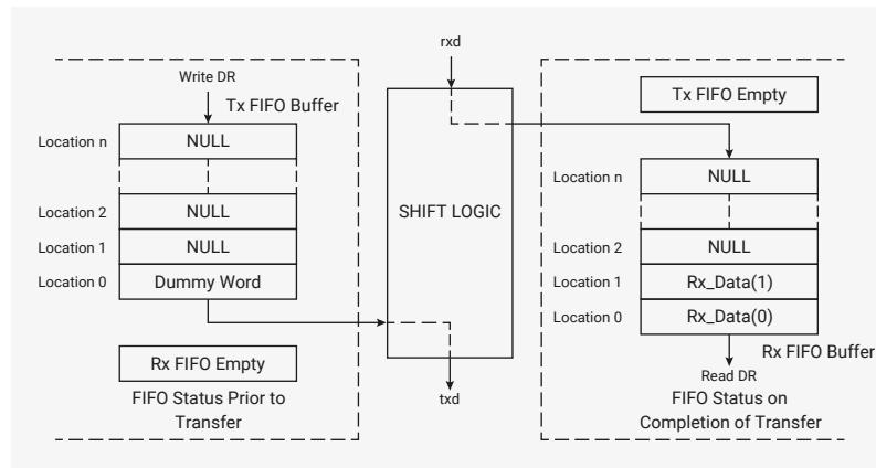
The diagram illustrates the FIFO status for receive-only SPI and SSP transfers. It is divided into two main sections: 'FIFO Status Prior to Transfer' and 'FIFO Status on Completion of Transfer', separated by a dashed line.
FIFO Status Prior to Transfer:
- Tx FIFO Buffer: A vertical stack of four locations. Location 0 contains 'Dummy Word', and Locations 1, 2, and n are 'NULL'. An arrow labeled 'Write DR' points to the top of this buffer.
- Rx FIFO Buffer: A single box labeled 'Rx FIFO Empty'.
- SHIFT LOGIC: A central block with 'rxd' input and 'txd' output.
FIFO Status on Completion of Transfer:
- Tx FIFO Buffer: All four locations (0, 1, 2, n) are now 'NULL'. An arrow labeled 'Tx FIFO Empty' points to the top of this buffer.
- Rx FIFO Buffer: A vertical stack of four locations. Location 0 contains 'Rx_Data(0)', Location 1 contains 'Rx_Data(1)', and Locations 2 and n are 'NULL'. An arrow labeled 'Read DR' points to the bottom of this buffer.
- SHIFT LOGIC: The same central block with 'rxd' input and 'txd' output.
Arrows indicate the flow of data from the Tx FIFO Buffer to the SHIFT LOGIC and from the SHIFT LOGIC to the Rx FIFO Buffer.
For eeprom_read transfers (transfer mode field [9:8] of the Control Register 0 = 11b), opcode and/or EEPROM address are written into the transmit FIFO. During transmission of these control frames, received data is not captured by the DW_apb_ssi master. After the control frames have been transmitted, receive data from the EEPROM is stored in the receive FIFO.
Figure 131 shows the FIFO levels prior to the beginning of a serial transfer and the FIFO levels on completion of the transfer. In this example, one opcode and an upper and lower address are transmitted to the EEPROM, and eight data frames are read from the EEPROM and stored in the receive FIFO of the DW_apb_ssi master.
Figure 131. FIFO Status for EEPROM Read Transfer Mode
![Diagram of FIFO status for EEPROM Read Transfer Mode. It shows two states: 'FIFO Status Prior to Transfer' and 'FIFO Status on Completion of Transfer'. In the first state, the Tx FIFO Buffer contains NULL at Location n, NULL at Location 3, Address[7:0] at Location 2, Address[15:8] at Location 1, and Opcode at Location 0. The Rx FIFO is empty. In the second state, the Tx FIFO is empty, and the Rx FIFO Buffer contains NULL at Location n, Rx_Data(7) at Location 7, Rx_Data(6) at Location 6, Rx_Data(1) at Location 1, and Rx_Data(0) at Location 0. A central SHIFT LOGIC block connects the two states, with rxd and txd lines.](/RP2040/6dcd40e2cead69fe534831cead2ff818_img.jpg)
The diagram illustrates the FIFO status for EEPROM Read Transfer Mode. It is divided into two main sections: 'FIFO Status Prior to Transfer' and 'FIFO Status on Completion of Transfer', connected by a central 'SHIFT LOGIC' block.
FIFO Status Prior to Transfer:
- Tx FIFO Buffer:
Contains data at various locations:
- Location n: NULL
- Location 3: NULL
- Location 2: Address[7:0]
- Location 1: Address[15:8]
- Location 0: Opcode
- Rx FIFO: Empty.
- Write DR: An arrow points to the Tx FIFO Buffer.
FIFO Status on Completion of Transfer:
- Tx FIFO: Empty.
- Rx FIFO Buffer:
Contains data at various locations:
- Location n: NULL
- Location 7: Rx_Data(7)
- Location 6: Rx_Data(6)
- Location 1: Rx_Data(1)
- Location 0: Rx_Data(0)
- Read DR: An arrow points to the Rx FIFO Buffer.
The central SHIFT LOGIC block has rx and tx lines connecting the two states.
4.10.10.2. Texas Instruments Synchronous Serial Protocol (SSP)
Data transfers begin by asserting the frame indicator line (ss_0_n/ss_in_n) for one serial clock period. Data to be transmitted are driven onto the txd line one serial clock cycle later; similarly data from the slave are driven onto the rxd line. Data are propagated on the rising edge of the serial clock (sclk_out/sclk_in) and captured on the falling edge. The length of the data frame ranges from four to 32 bits.
Figure 132 shows the timing diagram for a single SSP serial transfer.
Figure 132. SSP Serial Format
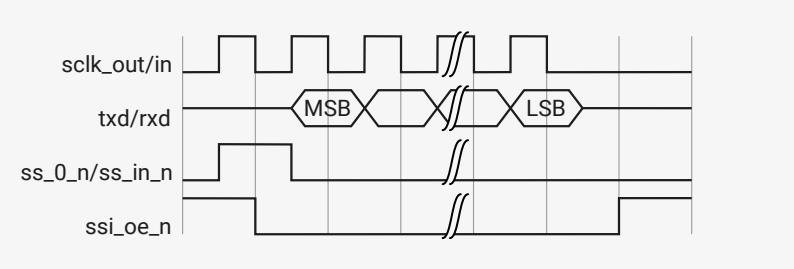
The timing diagram for a single SSP serial transfer shows four signals over time:
- sclk_out/in: A periodic serial clock signal.
- txd/rxd: The data bus. It shows a data frame with MSB (Most Significant Bit) and LSB (Least Significant Bit) labels.
- ss_0_n/ss_in_n: The frame indicator signal. It is asserted (goes high) for one clock period.
- ssi_oe_n: The output enable signal. It is asserted (goes low) for the duration of the transfer.
Continuous data frames are transferred in the same way as single data frames. The frame indicator is asserted for one clock period during the same cycle as the LSB from the current transfer, indicating that another data frame follows.
Figure 133 shows the timing for a continuous SSP transfer.
Figure 133. SSP Serial Format Continuous Transfer
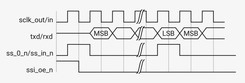
The timing diagram for a continuous SSP transfer shows four signals over time:
- sclk_out/in: A periodic serial clock signal.
- txd/rxd: The data bus. It shows a continuous stream of data frames with MSB (Most Significant Bit) and LSB (Least Significant Bit) labels.
- ss_0_n/ss_in_n: The frame indicator signal. It is asserted (goes high) for one clock period.
- ssi_oe_n: The output enable signal. It is asserted (goes low) for the duration of the transfer.
4.10.10.3. National Semiconductor Microwire
Data transmission begins with the falling edge of the slave-select signal (ss_0_n). One-half serial clock (sclk_out) period later, the first bit of the control is sent out on the txd line. The length of the control word can be in the range 1 to 16 bits and is set by writing bit field CFS (bits 15:12) in CTRLR0. The remainder of the control word is transmitted (propagated on the falling edge of sclk_out) by the DW_apb_ssi serial master. During this transmission, no data are present (high impedance) on the serial master's rxd line.
The direction of the data word is controlled by the MDD bit field (bit 1) in the Microwire Control Register (MWCR). When MDD=0, this indicates that the DW_apb_ssi serial master receives data from the external serial slave. One clock cycle after the LSB of the control word is transmitted, the slave peripheral responds with a dummy 0 bit, followed by the data frame, which can be four to 32 bits in length. Data are propagated on the falling edge of the serial clock and captured on the rising edge.
The slave-select signal is held active-low during the transfer and is de-asserted one-half clock cycle later, after the data are transferred. Figure 134 shows the timing diagram for a single DW_apb_ssi serial master read from an external serial slave.
Figure 134. Single DW_apb_ssi Master Microwire Serial Transfer (MDD=0)
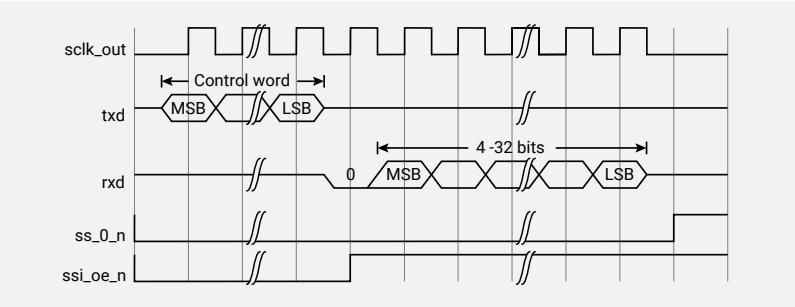
The diagram illustrates the timing for a single Microwire serial transfer where MDD=0. It shows five signals over time: sclk_out (serial clock), txd (transmit data), rxd (receive data), ss_0_n (slave select), and ssi_oe_n (serial output enable). The txd signal first transmits a control word (MSB to LSB), followed by a dummy 0 bit, and then a data frame (4-32 bits, MSB to LSB). The rxd signal shows the data frame (MSB to LSB) starting after the dummy 0 bit. The ss_0_n signal is active-low and stays low during the transfer. The ssi_oe_n signal is active-low and goes low during the transfer.
Figure 135 shows how the data and control frames are structured in the transmit FIFO prior to the transfer; the value programmed into the MWCR register is also shown.
Figure 135. FIFO Status for Single Microwire Transfer (receiving data frame)
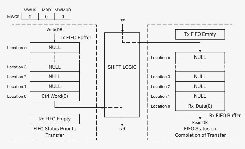
The diagram shows the FIFO status for a single Microwire transfer where MDD=0. It includes the MWCR register with fields MWHS, MDD, and MWMOD. The Tx FIFO Buffer contains NULL values for locations n, 3, 2, 1, and Ctrl Word(0). The Rx FIFO Buffer contains NULL values for locations n, 3, 2, 1, and Rx_Data(0). The SHIFT LOGIC block is shown between the Tx and Rx FIFOs. The Rx FIFO Empty signal is shown. The FIFO Status Prior to Transfer and FIFO Status on Completion of Transfer are shown.
Continuous transfers for the Microwire protocol can be sequential or nonsequential, and are controlled by the MWMOD bit field (bit 0) in the MWCR register.
Nonsequential continuous transfers occur as illustrated in Figure 136 , with the control word for the next transfer following immediately after the LSB of the current data word.
Figure 136. Continuous Nonsequential Microwire Transfer (receiving data frame)
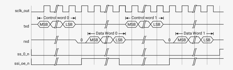
The diagram illustrates the timing for a continuous nonsequential Microwire serial transfer. It shows five signals over time: sclk_out (serial clock), txd (transmit data), rxd (receive data), ss_0_n (slave select), and ssi_oe_n (serial output enable). The txd signal shows Control word 0, followed by Data Word 0, then Control word 1, followed by Data Word 1. The rxd signal shows the data frame (MSB to LSB) starting after the dummy 0 bit. The ss_0_n signal is active-low and stays low during the transfer. The ssi_oe_n signal is active-low and goes low during the transfer.
The only modification needed to perform a continuous nonsequential transfer is to write more control words into the transmit FIFO buffer; this is illustrated in Figure 137 . In this example, two data words are read from the external serial-slave device.
Figure 137. FIFO Status for Nonsequential Microwire Transfer (receiving data frame)
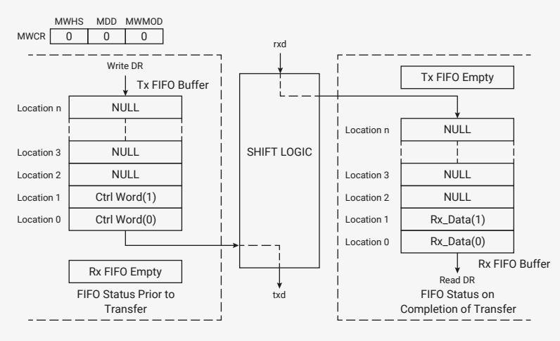
During sequential continuous transfers, only one control word is transmitted from the DW_apb_ssi master. The transfer is started in the same manner as with nonsequential read operations, but the cycle is continued to read further data. The slave device automatically increments its address pointer to the next location and continues to provide data from that location. Any number of locations can be read in this manner; the DW_apb_ssi master terminates the transfer when the number of words received is equal to the value in the CTRLR1 register plus one.
The timing diagram in Figure 138 and example in Figure 139 show a continuous sequential read of two data frames from the external slave device.
Figure 138. Continuous Sequential Microwire Transfer (receiving data frame)
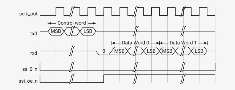
Figure 139. FIFO Status for Sequential Microwire Transfer (receiving data frame)
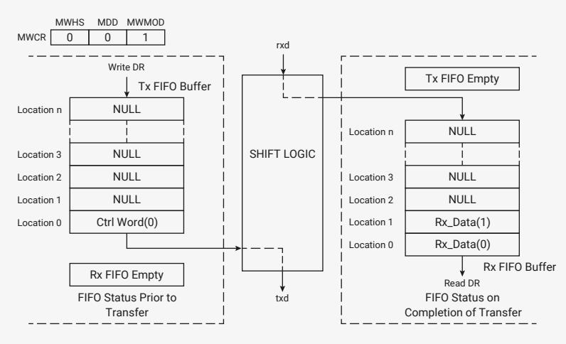
When MDD = 1, this indicates that the DW_apb_ssi serial master transmits data to the external serial slave. Immediately after the LSB of the control word is transmitted, the DW_apb_ssi master begins transmitting the data frame to the slave peripheral.
Figure 140 shows the timing diagram for a single DW_apb_ssi serial master write to an external serial slave.
Figure 140. Single Microwire Transfer (transmitting data frame)
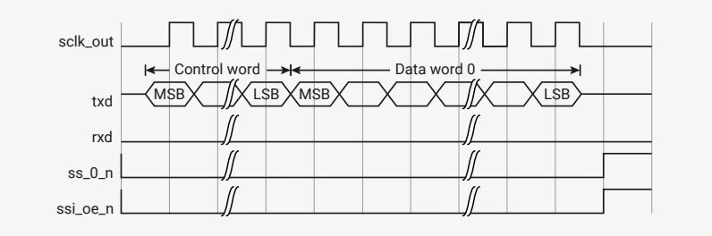
NOTE
The DW_apb_ssi does not support continuous sequential Microwire writes, where MDD = 1 and MWMOD = 1.
Figure 141 shows how the data and control frames are structured in the transmit FIFO prior to the transfer, also shown is the value programmed into the MWCR register.
Figure 141. FIFO Status for Single Microwire Transfer (transmitting data frame)
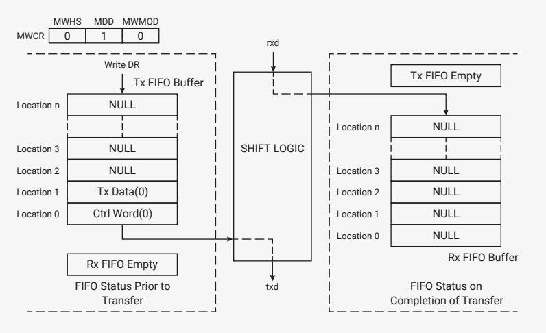
Continuous transfers occur as shown in Figure 142, with the control word for the next transfer following immediately after the LSB of the current data word.
Figure 142. Continuous Microwire Transfer (transmitting data frame)
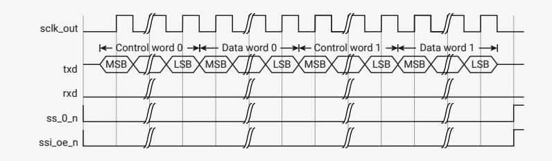
The only modification you need to make to perform a continuous transfer is to write more control and data words into the transmit FIFO buffer, shown in Figure 143. This example shows two data words are written to the external serial slave device.
Figure 143. FIFO Status for Continuous Microwire Transfer (transmitting data frame)
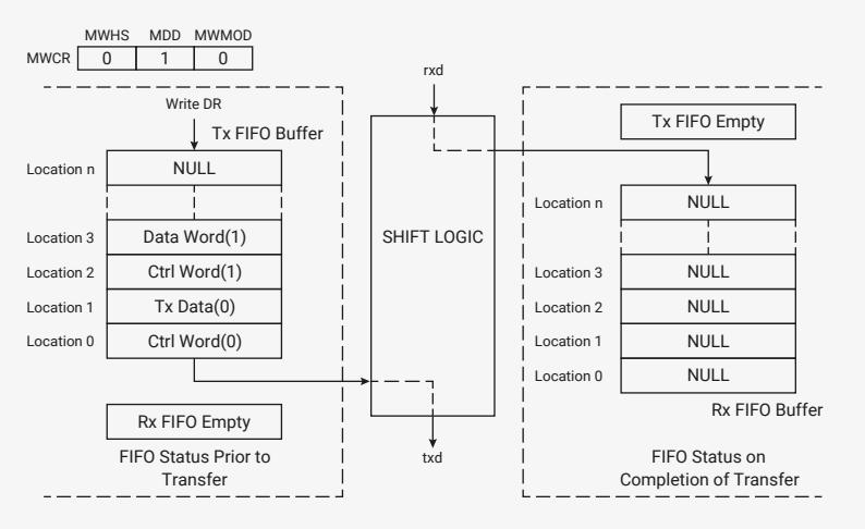
The Microwire handshaking interface can also be enabled for DW_apb_ssi master write operations to external serial-slave devices. To enable the handshaking interface, you must write 1 into the MHS bit field (bit 2) on the MWCR register. When MHS is set to 1, the DW_apb_ssi serial master checks for a ready status from the slave device before completing the transfer, or transmitting the next control word for continuous transfers.
Figure 144 shows an example of a continuous Microwire transfer with the handshaking interface enabled.
Figure 144. Continuous Microwire Transfer with Handshaking (transmitting data frame)
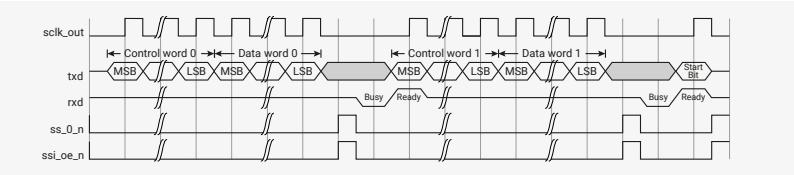
After the first data word has been transmitted to the serial-slave device, the DW_apb_ssi master polls the rxd input waiting for a ready status from the slave device. Upon reception of the ready status, the DW_apb_ssi master begins transmission of the next control word. After transmission of the last data frame has completed, the DW_apb_ssi master transmits a start bit to clear the ready status of the slave device before completing the transfer. The FIFO status for this transfer is the same as in Figure 143, except that the MWHS bit field is set (1).
To transmit a control word (not followed by data) to a serial-slave device from the DW_apb_ssi master, there must be only one entry in the transmit FIFO buffer. It is impossible to transmit two control words in a continuous transfer, as the shift logic in the DW_apb_ssi treats the second control word as a data word. When the DW_apb_ssi master transmits only a control word, the MDD bit field (bit 1 of MWCR register) must be set (1).
In the example shown in Figure 145 and in the timing diagram in Figure 146, the handshaking interface is enabled. If the handshaking interface is disabled (MHS=0), the transfer is terminated by the DW_apb_ssi master one sclk_out cycle after the LSB of the control word is captured by the slave device.
Figure 145. FIFO Status for Microwire Control Word Transfer
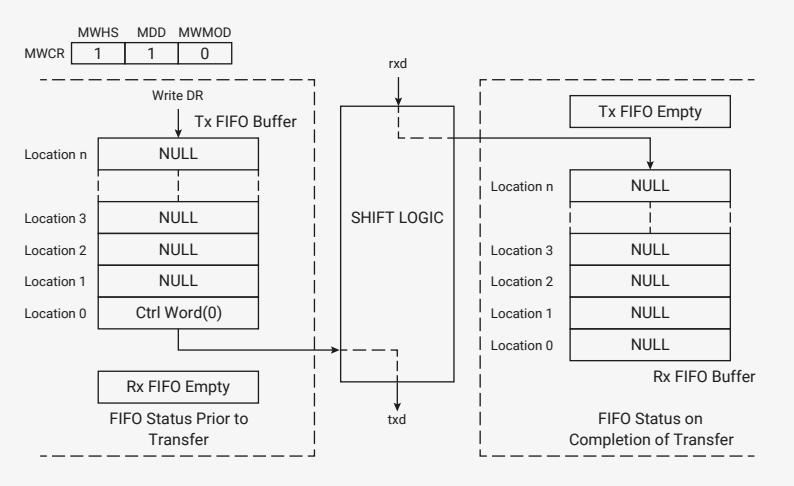
Figure 146. Microwire Control Word
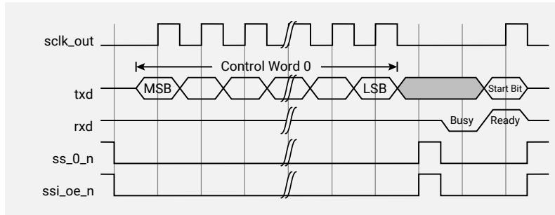
The diagram illustrates the Microwire Control Word timing. It shows five signals:
sclk_out
,
txd
,
rx
,
ss_0_n
, and
ssi_oe_n
. The
sclk_out
signal is a periodic clock. The
txd
signal shows a sequence of bits from MSB to LSB, followed by a Start Bit. The
rx
signal shows a Busy period followed by a Ready period. The
ss_0_n
and
ssi_oe_n
signals show a pulse during the Ready period.
4.10.10.4. Enhanced SPI Modes
DW_apb_ssi supports the dual and quad modes of SPI in RP2040; octal mode is not supported.
txd
,
rx
and
ssi_oe_n
signals are four bits wide.
Data is shifted out/in on more than one line, increasing the overall throughput. All four combinations of the serial clock's polarity and phase are valid in this mode and work the same as in normal SPI mode. Dual SPI, or Quad SPI modes function similarly except for the width of
txd
,
rx
and
ssi_oe_n
signals. The mode of operation (write/read) can be selected using the
CTRLR0.TMOD
field.
4.10.10.4.1. Write Operation in Enhanced SPI Modes
Dual, or Quad, SPI write operations can be divided into three parts:
- • Instruction phase
- • Address phase
- • Data phase
The following register fields are used for a write operation:
- •
CTRLR0.SPI_FRF- Specifies the format in which the transmission happens for the frame. - •
SPI_CTRLR0(Control Register 0 register) – Specifies length of instruction, address, and data. - •
SPI_CTRLR0.INST_L– Specifies length of an instruction (possible values for an instruction are 0, 4, 8, or 16 bits.) - •
SPI_CTRLR0.ADDR_L– Specifies address length (See Table 579 for decode values) - •
CTRLR0.DFSorCTRLR0.DFS_32– Specifies data length.
An instruction takes one FIFO location. An address can take more than one FIFO locations.
Both the instruction and address must be programmed in the data register (DR). DW_apb_ssi will wait until both have been programmed to start the write operation.
The instruction, address and data can be programmed to send in dual/quad mode, which can be selected from the
SPI_CTRLR0.TRANS_TYPE
and
CTRLR0.SPI_FRF
fields.
NOTE
- • If CTRLR0.SPI_FRF is selected to be "Standard SPI Format", everything is sent in Standard SPI mode and SPI_CTRLR0.TRANS_TYPE field is ignored.
- • CTRLR0.SPI_FRF is only applicable if CTRLR0.FRF is programmed to 00b.
Figure 147 shows a typical write operation in Dual, or Quad, SPI Mode. The value of N will be: 7 if SSI_SPI_MODE is set to 3, 3 if SSI_SPI_MODE is set to 2, and 1 if SSI_SPI_MODE is set to 1. For 1-write operation, the instruction and address are sent only once followed by data frames programmed in DR until the transmit FIFO becomes empty.
Figure 147. Typical Write Operation Dual/Quad SPI Mode
![Timing diagram for a typical write operation in Dual/Quad SPI Mode. The diagram shows four signals: sclk_out, txd[N:0], ssi_oe_n[N:0], and ss_oe_n. The txd[N:0] signal is divided into three sections: INSTRUCTION, ADDRESS, and DATA. The ssi_oe_n signal is active low and covers the INSTRUCTION and ADDRESS sections. The ss_oe_n signal is active low and covers the DATA section.](/RP2040/e6766df4a3bbd48e22e5467cd47fb47e_img.jpg)
To initiate a Dual/Quad write operation, CTRLR0.SPI_FRF must be set to 01/10/11, respectively. This will set the transfer type, and for each write command, data will be transferred in the format specified in CTRLR0.SPI_FRF field.
Case A: Instruction and address both transmitted in standard SPI format
For this, SPI_CTRLR0.TRANS_TYPE field must be set to 00b. Figure 148 shows the timing diagram when both instruction and address are transmitted in standard SPI format. The value of N will be: 7 if CTRLR0.SPI_FRF is set to 11b, 3 if CTRLR0.SPI_FRF is set to 10b, and 1 if CTRLR0.SPI_FRF is set to 01b.
Figure 148. Instruction and Address Transmitted in Standard SPI Format
![Timing diagram for Case A: Instruction and address both transmitted in standard SPI format. The diagram shows five signals: sclk_out, txd[0], txd[N-1:0], ss_oe_n[0], and ss_oe_n[N-1:0]. The txd[0] signal is divided into three sections: INSTRUCTION, ADDRESS, and DATA. The txd[N-1:0] signal is active low and covers the INSTRUCTION and ADDRESS sections. The ss_oe_n[0] signal is active low and covers the INSTRUCTION and ADDRESS sections. The ss_oe_n[N-1:0] signal is active low and covers the DATA section.](/RP2040/9a40c254094509a810f8b80041d2e7d4_img.jpg)
Case B: Instruction transmitted in standard and address transmitted in Enhanced SPI format
For this, SPI_CTRLR0.TRANS_TYPE field must be set to one. Figure 149 shows the timing diagram when an instruction is transmitted in standard format and address is transmitted in dual SPI format specified in the CTRLR0.SPI_FRF field. The value of N will be: 7 if CTRLR0.SPI_FRF is set to 11b, 3 if CTRLR0.SPI_FRF is set to 10b, and 1 if CTRLR0.SPI_FRF is set to 01b.
Figure 149. Instruction Transmitted in Standard and Address Transmitted in Enhanced SPI Format
![Timing diagram for Case B: Instruction transmitted in standard and address transmitted in Enhanced SPI format. The diagram shows five signals: sclk_out, txd[0], txd[N-1:0], ss_oe_n[0], and ss_oe_n[N-1:0]. The txd[0] signal is divided into three sections: INSTRUCTION, ADDRESS, and DATA. The txd[N-1:0] signal is active low and covers the INSTRUCTION and ADDRESS sections. The ss_oe_n[0] signal is active low and covers the INSTRUCTION and ADDRESS sections. The ss_oe_n[N-1:0] signal is active low and covers the DATA section.](/RP2040/50774a8583b762f7d7440ecbade23d2b_img.jpg)
Case C: Instruction and Address both transmitted in Enhanced SPI format
For this, SPI_CTRLR0.TRANS_TYPE field must be set to 10b. Figure 150 shows the timing diagram in which instruction and address are transmitted in SPI format specified in the CTRLR0.SPI_FRF field. The value of N will be: 7 if CTRLR0.SPI_FRF is set to 11b, 3 if CTRLR0.SPI_FRF is set to 10b, and 1 if CTRLR0.SPI_FRF is set to 01b.
Figure 150. Instruction and Address Both Transmitted in Enhanced SPI Format
![Timing diagram for Case C: Instruction and Address both transmitted in Enhanced SPI format. The diagram shows four signals: sclk_out, txd[N:0], ssi_oe_n[N:0], and ss_0_n. The txd[N:0] signal is divided into three sections: INSTRUCTION, ADDRESS, and DATA. The ssi_oe_n[N:0] signal is active low and covers the INSTRUCTION and ADDRESS sections. The ss_0_n signal is active low and covers the DATA section.](/RP2040/102d454eaa01f008a4068add3d41a9fa_img.jpg)
Case D: Instruction only transfer in enhanced SPI format
For this, SPI_CTRLR0.TRANS_TYPE field must be set to 10b. Figure 151 shows the timing diagram for such a transfer. The value of N will be: 7 if CTRLR0.SPI_FRF is set to 11b, 3 if CTRLR0.SPI_FRF is set to 10b, and 1 if
CTRLR0.SPI_FRF is set to 01b.
Figure 151. Instruction only transfer in enhanced SPI Format
![Timing diagram for Figure 151 showing sclk_out, txd[N:0], ssL_oe_n[N:0], and ss_0_n signals. The txd[N:0] signal contains the INSTRUCTION data.](/RP2040/358abc2a30e04e387549d81724174e61_img.jpg)
The diagram shows four signals over time: sclk_out (clock), txd[N:0] (transmit data), ssL_oe_n[N:0] (slave select output enable), and ss_0_n (slave select output). The txd[N:0] signal is active during the INSTRUCTION phase. The ssL_oe_n[N:0] signal is active during the INSTRUCTION phase. The ss_0_n signal is active during the INSTRUCTION phase.
4.10.10.4.2. Read Operation in Enhanced SPI Modes
A Dual, or Quad, SPI read operation can be divided into four phases:
- • Instruction phase
- • Address phase
- • Wait cycles
- • Data phase
Wait Cycles can be programmed using SPI_CTRLR0.WAIT_CYCLES field. The value programmed into SPI_CTRLR0.WAIT_CYCLES is mapped directly to sclk_out times. For example, WAIT_CYCLES=0 indicates no Wait, WAIT_CYCLES=1, indicates one wait cycle and so on. The wait cycles are introduced for target slave to change their mode from input to output and the wait cycles can vary for different devices.
For a READ operation, DW_apb_ssi sends instruction and control data once and waits until it receives NDF (CTRLR1 register) number of data frames and then de-asserts slave select signal.
Figure 152 shows a typical read operation in dual quad SPI mode. The value of N will be: 3 if SSI_SPI_MODE is set to Quad mode, and 1 if SSI_SPI_MODE is set to Dual mode.
Figure 152. Typical Read Operation in Enhanced SPI Mode
![Timing diagram for Figure 152 showing sclk_out, txd[N:0], rxd[N:0], ssL_oe_n[N:0], and ss_0_n signals. The txd[N:0] signal contains INSTRUCTION, ADDRESS, and WAIT CYCLES. The rxd[N:0] signal contains DATA.](/RP2040/3bc79190b437fe6fd69b02c8152c0194_img.jpg)
The diagram shows five signals over time: sclk_out (clock), txd[N:0] (transmit data), rxd[N:0] (receive data), ssL_oe_n[N:0] (slave select output enable), and ss_0_n (slave select output). The txd[N:0] signal contains INSTRUCTION, ADDRESS, and WAIT CYCLES. The rxd[N:0] signal contains DATA. The ssL_oe_n[N:0] signal is active during the INSTRUCTION, ADDRESS, and WAIT CYCLES phases. The ss_0_n signal is active during the INSTRUCTION, ADDRESS, and WAIT CYCLES phases.
To initiate a dual/quad read operation, CTRLR0.SPI_FRF must be set to 01/10/11 respectively. This will set the transfer type, now for each read command data will be transferred in the format specified in CTRLR0.SPI_FRF field.
Following are the possible cases of write operation in enhanced SPI modes:
Case A: Instruction and address both transmitted in standard SPI format
For this, SPI_CTRLR0.TRANS_TYPE field should be set to 00b. Figure 153 shows the timing diagram when both instruction and address are transferred in standard SPI format. The figure also shows WAIT cycles after address, which can be programmed in the SPI_CTRLR0.WAIT_CYCLES field. The value of N will be 7 if CTRLR0.SPI_FRF is set to 11b, 3 if CTRLR0.SPI_FRF is set to 10b, and 1 if CTRLR0.SPI_FRF is set to 01b.
Figure 153. Instruction and Address Transmitted in Standard SPI Format
![Timing diagram for Figure 153 showing sclk_out, txd[0], txd[N-1:0], rxd[N:0], ssL_oe_n[0], ssL_oe_n[N-1:0], and ss_0_n signals. The txd[0] signal contains INSTRUCTION. The txd[N-1:0] signal contains ADDRESS. The rxd[N:0] signal contains DATA.](/RP2040/ae5f7c74f295b4316b6f4ca77529924d_img.jpg)
The diagram shows seven signals over time: sclk_out (clock), txd[0] (transmit data), txd[N-1:0] (transmit data), rxd[N:0] (receive data), ssL_oe_n[0] (slave select output enable), ssL_oe_n[N-1:0] (slave select output enable), and ss_0_n (slave select output). The txd[0] signal contains INSTRUCTION. The txd[N-1:0] signal contains ADDRESS. The rxd[N:0] signal contains DATA. The ssL_oe_n[0] signal is active during the INSTRUCTION, ADDRESS, and WAIT CYCLES phases. The ssL_oe_n[N-1:0] signal is active during the INSTRUCTION, ADDRESS, and WAIT CYCLES phases. The ss_0_n signal is active during the INSTRUCTION, ADDRESS, and WAIT CYCLES phases.
Case B: Instruction transmitted in standard and address transmitted in dual SPI format
For this, SPI_CTRLR0.TRANS_TYPE field should be set to 01b. Figure 154 shows the timing diagram in which instruction is transmitted in standard format and address is transmitted in dual SPI format. The value of N will be 7 if CTRLR0.SPI_FRF is set to 11b, 3 if CTRLR0.SPI_FRF is set to 10b, and 1 if CTRLR0.SPI_FRF is set to 01b.
Figure 154. Instruction Transmitted in Standard and Address Transmitted in Enhanced SPI Format
![Timing diagram for Figure 154 showing SPI signals: sclk_out, txd[0], txd[N-1:0], rxd[N:0], ssi_oe_n[0], ssi_oe_n[N-1:0], and ss_o_n. The diagram shows the sequence of instruction and address transmission in standard and enhanced SPI formats.](/RP2040/31726f761cbbda3f2e76eefdbbef084a_img.jpg)
The diagram shows the timing of SPI signals. ss_o_n is active low and goes low at the start of the transfer. ss_i_oe_n[0] and ss_i_oe_n[N-1:0] are active low and go high at the start of the transfer. txd[0] and txd[N-1:0] transmit the instruction and address. rxd[N:0] receives the data. sclk_out is the serial clock. The diagram shows the sequence of instruction and address transmission in standard and enhanced SPI formats.
Case C: Instruction and Address both transmitted in Dual SPI format
For this, SPI_CTRLR0.TRANS_TYPE field must be set to 10b . Figure 155 shows the timing diagram in which both instruction and address are transmitted in dual SPI format. The value of N will be: 7 if CTRLR0.SPI_FRF is set to 11b , 3 if CTRLR0.SPI_FRF is set to 10b , and 1 if CTRLR0.SPI_FRF is set to 01b .
Figure 155. Instruction and Address Transmitted in Enhanced SPI Format
![Timing diagram for Figure 155 showing SPI signals: sclk_out, txd[N:0], rxd[N:0], ssi_oe_n[N:0], and ss_o_n. The diagram shows the sequence of instruction and address transmission in enhanced SPI format.](/RP2040/0d22641ea83ac2e2a5b26457b97d06ce_img.jpg)
The diagram shows the timing of SPI signals. ss_o_n is active low and goes low at the start of the transfer. ss_i_oe_n[N:0] is active low and goes high at the start of the transfer. txd[N:0] transmits the instruction and address. rxd[N:0] receives the data. sclk_out is the serial clock. The diagram shows the sequence of instruction and address transmission in enhanced SPI format.
Case D: No Instruction, No Address READ transfer
For this, SPI_CTRLR0.ADDR_L and SPI_CTRLR0.INST_L must be set to 0 and SPI_CTRLR0.WAIT_CYCLES must be set to a non-zero value. Table 579 lists the ADDR_L decode value and the respective description for enhanced (Dual/Quad) SPI modes.
Table 579. ADDR_L Decode in Enhanced SPI Mode
| ADDR_L Decode Value | Description |
|---|---|
| 0000 | 0-bit Address Width |
| 0001 | 4-bit Address Width |
| 0010 | 8-bit Address Width |
| 0011 | 12-bit Address Width |
| 0100 | 16-bit Address Width |
| 0101 | 20-bit Address Width |
| 0110 | 24-bit Address Width |
| 0111 | 28-bit Address Width |
| 1000 | 32-bit Address Width |
| 1001 | 36-bit Address Width |
| 1010 | 40-bit Address Width |
| 1011 | 44-bit Address Width |
| 1100 | 48-bit Address Width |
| 1101 | 52-bit Address Width |
| 1110 | 56-bit Address Width |
| 1111 | 60-bit Address Width |
Figure 156 shows the timing diagram for such type of transfer. The value of N will be: 7 if CTRLR0.SPI_FRF is set to 11b , 3 if CTRLR0.SPI_FRF is set to 10b , and 1 if CTRLR0.SPI_FRF is set to 01b . To initiate this transfer, the software has to perform a dummy write in the data register (DR), DW_apb_ssi will wait for programmed wait cycles and then fetch the amount of data specified in NDF field.
Figure 156. No Instruction and No Address READ Transfer
![Timing diagram for Figure 156 showing signals: sclk_out, txd[N:0], rxd[N:0], ssi_oe_n[N:0], and ss_0_n. The diagram illustrates a sequence of operations where the txd[N:0] signal is high during 'WAIT CYCLES' and then transitions to a 'DATA' phase. The rxd[N:0] signal is high during the 'DATA' phase. The ssi_oe_n[N:0] signal is high during the 'WAIT CYCLES' phase and then transitions to a low state. The ss_0_n signal is high during the 'WAIT CYCLES' phase and then transitions to a low state.](/RP2040/014ecafcfe5066ed6c217297b8fe83c8_img.jpg)
4.10.10.4.3. Advanced I/O Mapping for Enhanced SPI Modes
The Input/Output mapping for enhanced SPI modes (dual, and quad) is hardcoded inside the DW_apb_ssi. The rxd[1] signal will be used to sample incoming data in standard SPI mode of operation.
For other protocols (such as SSP and Microwire), the I/O mapping remains the same. Therefore, it is easy for other protocols to connect with any device that supports Dual/Quad SPI operation because other protocols do not require a MUX logic to exist outside the design.
Figure 157 shows the I/O mapping of DW_apb_ssi in Quad mode with another SPI device that supports the Quad mode. As illustrated in Figure 157, the IO[1] pin is used as DO in standard SPI mode of operation and it is connected to rxd[1] pin, which will be sampling the input in the standard mode of operation.
Figure 157. Advanced I/O Mapping in Quad SPI Modes
![Block diagram for Figure 157 showing the I/O mapping of DW_apb_ssi in Quad SPI mode. The DW_apb_ssi block has signals txd[3], rxd[3], txd[2], rxd[2], txd[1], rxd[1], txd[0], and rxd[0]. These signals are connected to four IO Buffers. The IO Buffers are connected to the SPI slave Device signals IO[3], IO[2], IO[1]/DO, and IO[0]/DI. The IO[1]/DO signal is connected to the rxd[1] signal of the DW_apb_ssi block.](/RP2040/bcc96fa6e8fa30df412515edbeee32d6_img.jpg)
4.10.10.5. Dual Data-Rate (DDR) Support in SPI Operation
In standard operations, data transfer in SPI modes occur on either the positive or negative edge of the clock. For improved throughput, the dual data-rate transfer can be used for reading or writing to the memories.
The DDR mode supports the following modes of SPI protocol:
- • SCPH=0 & SCPOL=0 (Mode 0)
- • SCPH=1 & SCPOL=1 (Mode 3)
DDR commands enable data to be transferred on both edges of clock. Following are the different types of DDR commands:
- • Address and data are transmitted (or received in case of data) in DDR format, while instruction is transmitted in standard format.
- • Instruction, address, and data are all transmitted or received in DDR format.
The DDR_EN (SPI_CTRLR0[16]) bit is used to determine if the Address and data have to be transferred in DDR mode and INST_DDR_EN (SPI_CTRLR0[17]) bit is used to determine if Instruction must be transferred in DDR format. These bits
are only valid when the CTRLR0.SPI_FRF bit is set to be in Dual, or Quad mode.
Figure 158 describes a DDR write transfer where instructions are continued to be transmitted in standard format. In Figure 158, the value of N will be 7 if CTRLR0.SPI_FRF is set to 11b, 3 if CTRLR0.SPI_FRF is set to 10b, and 1 if CTRLR0.SPI_FRF is set to 01b.
Figure 158. DDR Transfer with SCPH=0 and SCPOL=0
![Timing diagram for Figure 158 showing a DDR write transfer with SCPH=0 and SCPOL=0. The diagram tracks signals: sclk_out (clock), ss_oe_n (active low chip select), txd[N:0] (transmit data), rxd[N:0] (receive data), and ss_oe_n[N:0]. The txd[N:0] signal begins with an instruction phase (INST) in standard format, followed by address bytes (A3, A2, A1, A0) and data bytes (D3, D2, D1, D0) transmitted on both edges of sclk_out. Legend: INST = Instruction Phase; A3, A2, A1, A0 = Address Bytes; D3, D2, D1, D0 = Data Bytes.](/RP2040/ae11c60feb544e83a0ef802bf234adc0_img.jpg)
Figure 159 describes a DDR write transfer where instruction, address and data all are transferred in DDR format.
Figure 159. DDR Transfer with Instruction, Address and Data Transmitted in DDR Format
![Timing diagram for Figure 159 showing a DDR write transfer where all phases are in DDR format. Signals include sclk_out, ss_0_n, txd[N:0], rxd[N:0], and ssi_oe_n[N:0]. The txd[N:0] line shows two instruction bytes (INST-1, INST-2) followed by address bytes (A3, A2, A1, A0) and data bytes (D3, D2, D1, D0), all changing on both rising and falling edges of sclk_out. Legend: INST-1, INST-2 = Instruction Bytes; A3, A2, A1, A0 = Address Bytes; D3, D2, D1, D0 = Data Bytes.](/RP2040/9ef050ef6cbd305f87b3b3cecba84a45_img.jpg)
NOTE
In the DDR transfer, address and instruction cannot be programmed to a value of 0.
4.10.10.5.1. Transmitting Data in DDR Mode
In DDR mode, data is transmitted on both edges so that it is difficult to sample data correctly. DW_apb_ssi uses an internal register to determine the edge on which the data should be transmitted. This will ensure that the receiver is able to get a stable data while sampling. The internal register (DDR_DRIVE_EDGE) determines the edge on which the data is transmitted. DW_apb_ssi sends data with respect to baud clock, which is an integral multiple of the internal clock ( \( ssi\_clk * BAUDR \) ). The data needs to be transmitted within half clock cycle ( \( BAUDR/2 \) ), therefore the maximum value for DDR_DRIVE_EDGE is equal to \( [(BAUDR/2)-1] \) . If the programmed value of DDR_DRIVE_EDGE is 0 then data is transmitted edge-aligned with respect to sclk_out (baud clock). If the programmed value of DDR_DRIVE_EDGE is one then the data is transmitted one ssi_clk before the edge of sclk_out.
NOTE
If the baud rate is programmed to be two, then the data will always be edge aligned.
Figure 160, Figure 161, and Figure 162 show examples of how data is transmitted using different values of the DDR_DRIVE_EDGE register. The green arrows in these examples represent the points where data is driven. Baud rate used in all these examples is 12. In Figure 160, transmit edge and driving edge of the data are the same. This is default behavior in DDR mode.
Figure 160. Transmit Data With DDR_DRIVE_EDGE = 0
![Timing diagram for Figure 160 showing transmit data with DDR_DRIVE_EDGE = 0. Signals include ssi_clk (high frequency internal clock), sclk_out (baud clock), ss_0_n, txd[N:0], rxd[N:0], and ssi_oe_n[N:0]. Green arrows indicate that data transitions on txd[N:0] are aligned exactly with the edges of sclk_out. The sequence on txd[N:0] is INST, A3, A2, A1, A0, D3, D2, D1, D0. Legend: INST = Instruction Phase; A3, A2, A1, A0 = Address Bytes; D3, D2, D1, D0 = Data Bytes.](/RP2040/c4a023e1fe87d37f0e5e6a2241b43cbf_img.jpg)
Figure 160 shows the default behavior in which the transmit and driving edge of the data is the same.
Figure 161. Transmit Data With \( DDR\_DRIVE\_EDGE = 1 \)
![Timing diagram for Figure 161 showing transmit data with DDR_DRIVE_EDGE = 1. The diagram includes signals: ssi_clk, sclk_out, ss_0_n, txd[N:0], rxd[N:0], and ssi_oe_n[N:0]. The txd[N:0] signal shows an instruction phase (INST) followed by address bytes (A3, A2, A1, A0) and data bytes (D3, D2, D1, D0). The ssi_oe_n[N:0] signal is active (low) during the instruction and address phases. The legend indicates: INST = Instruction Phase, A3, A2, A1, A0 = Address Bytes, D3, D2, D1, D0 = Data Bytes. In this mode, data transitions on txd[N:0] occur on the falling edge of sclk_out.](/RP2040/6b74f92c0b63e1f3aadb1773646f7e92_img.jpg)
Figure 162. Transmit Data With \( DDR\_DRIVE\_EDGE = 2 \)
![Timing diagram for Figure 162 showing transmit data with DDR_DRIVE_EDGE = 2. The diagram includes signals: ssi_clk, sclk_out, ss_0_n, txd[N:0], rxd[N:0], and ssi_oe_n[N:0]. The txd[N:0] signal shows an instruction phase (INST) followed by address bytes (A3, A2, A1, A0) and data bytes (D3, D2, D1, D0). The ssi_oe_n[N:0] signal is active (low) during the instruction and address phases. The legend indicates: INST = Instruction Phase, A3, A2, A1, A0 = Address Bytes, D3, D2, D1, D0 = Data Bytes. In this mode, data transitions on txd[N:0] occur on the rising edge of sclk_out.](/RP2040/e48e44dc323fc70838f2d4a424022bcf_img.jpg)
4.10.10.6. XIP Mode Support in SPI Mode
The eXecute In Place (XIP) mode enables transfer of SPI data directly through the APB interface without writing the data register of DW_apb_ssi. XIP mode is enabled in DW_apb_ssi when the XIP cache is enabled. This control signal indicates whether APB transfers are register read-write or XIP reads. When in XIP mode, DW_apb_ssi expects only read request on the APB interface. This request is translated to SPI read on the serial interface and soon after the data is received, the data is returned to the APB interface in the same transaction.
NOTE
- • Only APB reads are supported during an XIP operation
The address length is derived from the SPI_CTRLR0.ADDR_L field, and relevant bits from paddr ( \( [SPI\_CTRLR0.ADDR\_L-1:0] \) ) are transferred as address to the SPI interface. XIP address is managed by the XIP cache controller.
4.10.10.6.1. Read Operation in XIP Mode
The XIP operation is supported only in enhanced SPI modes (Dual, Quad) of operation. Therefore, the CTRLR0.SPI_FRF bit should not be programmed to 0. An XIP read operation is divided into two phases:
- • Address phase
- • Data phase
For an XIP read operation
- 1. Set the SPI frame format and data frame size value in CTRLR0 register. Note that the value of the maximum data frame size is 32.
- 2. Set the Address length, Wait cycles, and transaction type in the SPI_CTRLR0 register. Note that the maximum address length is 32.
After these settings, a user can initiate a read transaction through the APB interface which will transferred to SPI peripheral using programmed values. Figure 163 shows the typical XIP transfer. The Value of N = 1, 3 and 7 for SPI mode Dual, and Quad modes, respectively.
Figure 163. Typical Read Operation in XIP Mode
![Timing diagram for a typical read operation in XIP mode. The diagram shows signals: pclk, xip_en, psel, penable, paddr, pready, prdata[31:0], ss_x_n, sclk_out, txd[N:0], and rxd[N:0]. The pclk is a periodic clock. xip_en is active high. psel is active high. penable is active high. paddr is 0x00. pready is active high. prdata[31:0] shows data D1. ss_x_n is active low. sclk_out is active high. txd[N:0] shows data 0x00. rxd[N:0] shows data D1. Blue arrows indicate data flow from prdata to txd and from rxd to prdata.](/RP2040/412796d8f3fd911a5a215d4d11887495_img.jpg)
4.10.11. DMA Controller Interface
The DW_apb_ssi has built-in DMA capability; it has a handshaking interface to a DMA Controller to request and control transfers. The APB bus is used to perform the data transfer to or from the DMA.
NOTE
When the DW_apb_ssi interfaces to the DMA controller, the DMA controller is always a flow controller; that is, it controls the block size. This must be programmed by software in the DMA controller.
The DW_apb_ssi uses two DMA channels, one for the transmit data and one for the receive data. The DW_apb_ssi has these DMA registers:
DMACR
Control register to enable DMA operation.
DMATDLR
Register to set the transmit the FIFO level at which a DMA request is made.
DMARDLR
Register to set the receive FIFO level at which a DMA request is made.
The DW_apb_ssi uses the following handshaking signals to interface with the DMA controller.
- • dma_tx_req
- • dma_tx_single
- • dma_tx_ack
- • dma_rx_req
- • dma_tx_req
- • dma_tx_single
- • dma_tx_ack
- • dma_rx_req
To enable the DMA Controller interface on the DW_apb_ssi, you must write the DMA Control Register (DMACR). Writing a 1 into the TDMAE bit field of DMACR register enables the DW_apb_ssi transmit handshaking interface. Writing a 1 into the RDMAE bit field of the DMACR register enables the DW_apb_ssi receive handshaking interface.
Table 580 provides description for different DMA transmit data level values.
Table 580. DMA Transmit Data Level (DMATDL) Decode Value
| DMATDL Value | Description |
|---|---|
| 0000_0000 | dma_tx_req is asserted when zero data entries are present in the transmit FIFO |
| 0000_0001 | dma_tx_req is asserted when one or less data entry is present in the transmit FIFO |
| 0000_0010 | dma_tx_req is asserted when two or less data entries are present in the transmit FIFO |
| ... | ... |
| 0000_1101 | dma_tx_req is asserted when 13 or less data entries are present in the transmit FIFO |
| 0000_1110 | dma_tx_req is asserted when 14 or less data entries are present in the transmit FIFO |
| 0000_1111 | dma_tx_req is asserted when 15 or less data entries are present in the transmit FIFO |
Table 581 provides description for different DMA Receive Data Level values.
Table 581. DMA
Receive Data Level
(DMARDL) Decode
Value
| DMARDL Value | Description |
|---|---|
| 0000_0000 | dma_rx_req is asserted when one or more data entries are present in the receive FIFO |
| 0000_0001 | dma_rx_req is asserted when two or more data entries are present in the receive FIFO |
| 0000_0010 | dma_rx_req is asserted when three or more data entries are present in the receive FIFO |
| ... | ... |
| 0000_1101 | dma_rx_req is asserted when 14 or more data entries are present in the receive FIFO |
| 0000_1110 | dma_rx_req is asserted when 15 or more data entries are present in the receive FIFO |
| 0000_1111 | dma_rx_req is asserted when 16 data entries are present in the receive FIFO |
4.10.11.1. Overview of Operation
As a block flow control device, the DMA Controller is programmed by the processor with the number of data items (block size) that are to be transmitted or received by the DW_apb_ssi.
The block is broken into a number of transactions, each initiated by a request from the DW_apb_ssi. The DMA Controller must also be programmed with the number of data items (in this case, DW_apb_ssi FIFO entries) to be transferred for each DMA request. This is also known as the burst transaction length.
Figure 164 shows a single block transfer, where the block size programmed into the DMA Controller is 12 and the burst transaction length is set to four. In this case, the block size is a multiple of the burst transaction length; therefore, the DMA block transfer consists of a series of burst transactions.
 CAUTION
On RP2040, the burst transaction length of the SSI's DMA interface is fixed at four transfers.
SSI.DMARDLR
must always be equal to 4, which is the value it takes at reset. The SSI will then request a single transfer when it has between one and three items in its FIFO, and a 4-burst when it has four or more.
Figure 164.
Breakdown of DMA
Transfer into Burst
Transactions. Block
size,
\(
\text{DMA\_CTLx.BLOCKS\_TS} =
\)
12. Number of data
items per source burst
transaction,
\(
\text{DMA\_CTLx.SRC\_MSIZE} =
\)
4. SSI receive FIFO
watermark level,
\(
\text{SSI\_DMARDLR} + 1 =
\)
\(
\text{DMA\_CTLx.SRC\_MSIZE} =
\)
4
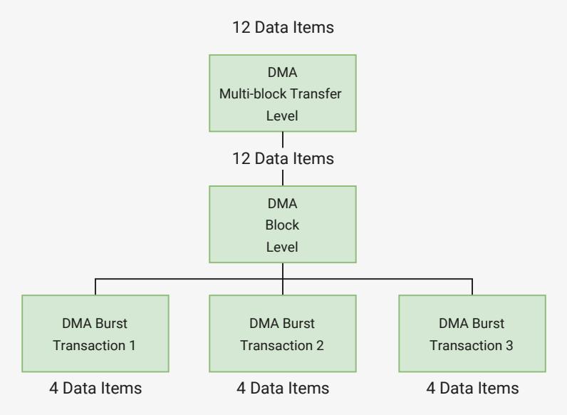
graph TD
    A[12 Data Items] --> B[DMA Multi-block Transfer Level]
    B --> C[12 Data Items]
    C --> D[DMA Block Level]
    D --> E1[DMA Burst Transaction 1]
    D --> E2[DMA Burst Transaction 2]
    D --> E3[DMA Burst Transaction 3]
    E1 --> F1[4 Data Items]
    E2 --> F2[4 Data Items]
    E3 --> F3[4 Data Items]
If the DW_apb_ssi makes a transmit request to this channel, four data items are written to the DW_apb_ssi transmit FIFO. Similarly, if the DW_apb_ssi makes a receive request to this channel, four data items are read from the DW_apb_ssi receive FIFO. Three separate requests must be made to this DMA channel before all 12 data items are written or read.
When the block size programmed into the DMA Controller is not a multiple of the burst transaction length, as shown in Figure 165 , a series of burst transactions followed by single transactions are needed to complete the block transfer.
Figure 165.
Breakdown of DMA
Transfer into Single
and Burst
Transactions. Block
size,
\(
\text{DMA\_CTLx.BLOCK\_TS} =
\)
15. Number of data
items per burst
transaction,
\(
\text{DMA\_CTLx.DEST\_MSIZE} =
\)
4. SSI transmit FIFO
watermark level,
\(
\text{SSI\_DMATDLR} =
\)
\(
\text{DMA\_CTLx.DEST\_MSIZE} =
\)
4
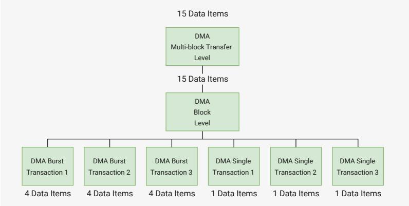
graph TD
    A[15 Data Items] --> B[DMA Multi-block Transfer Level]
    B --> C[15 Data Items]
    C --> D[DMA Block Level]
    D --> E1[DMA Burst Transaction 1]
    D --> E2[DMA Burst Transaction 2]
    D --> E3[DMA Burst Transaction 3]
    D --> F1[DMA Single Transaction 1]
    D --> F2[DMA Single Transaction 2]
    D --> F3[DMA Single Transaction 3]
    E1 --> G1[4 Data Items]
    E2 --> G2[4 Data Items]
    E3 --> G3[4 Data Items]
    F1 --> H1[1 Data Items]
    F2 --> H2[1 Data Items]
    F3 --> H3[1 Data Items]
4.10.12. APB Interface
The host processor accesses data, control, and status information on the DW_apb_ssi through the APB interface. APB accesses to the DW_apb_ssi peripheral are described in the following subsections.
4.10.12.1. Control and Status Register APB Access
Control and status registers within the DW_apb_ssi are byte-addressable. The maximum width of the control or status register in the DW_apb_ssi is 16 bits. Therefore all read and write operations to the DW_apb_ssi control and status registers require only one APB access.
4.10.12.2. Data Register APB Access
The data register (DR) within the DW_apb_ssi is 32 bits wide in order to remain consistent with the maximum serial transfer size (data frame). An APB write operation to DR moves data from pwwdata into the transmit FIFO buffer. An APB read operation from DR moves data from the receive FIFO buffer onto prdata.
The DW_apb_ssi DR can be written/read in one APB access.
i NOTE
The DR register in the DW_apb_ssi occupies sixty-four 32-bit locations of the memory map to facilitate AHB burst transfers. There are no burst transactions on the APB bus itself, but DW_apb_ssi supports the AHB bursts that happen on the AHB side of the AHB/APB bridge. Writing to any of these address locations has the same effect as pushing the data from the pwwdata bus into the transmit FIFO. Reading from any of these locations has the same effect as popping data from the receive FIFO onto the prdata bus. The FIFO buffers on the DW_apb_ssi are not addressable.
4.10.13. List of Registers
The SSI registers start at a base address of
0x18000000
(defined as
XIP_SSI_BASE
in SDK).
Table 582. List of SSI registers
| Offset | Name | Info |
|---|---|---|
| 0x00 | CTRLR0 | Control register 0 |
| 0x04 | CTRLR1 | Master Control register 1 |
| 0x08 | SSIENR | SSI Enable |
| 0x0c | MWCR | Microwire Control |
| 0x10 | SER | Slave enable |
| 0x14 | BAUDR | Baud rate |
| 0x18 | TXFTLR | TX FIFO threshold level |
| 0x1c | RXFTLR | RX FIFO threshold level |
| 0x20 | TXFLR | TX FIFO level |
| 0x24 | RXFLR | RX FIFO level |
| 0x28 | SR | Status register |
| 0x2c | IMR | Interrupt mask |
| 0x30 | ISR | Interrupt status |
| 0x34 | RISR | Raw interrupt status |
| 0x38 | TXOICR | TX FIFO overflow interrupt clear |
| 0x3c | RXOICR | RX FIFO overflow interrupt clear |
| 0x40 | RXUICR | RX FIFO underflow interrupt clear |
| 0x44 | MSTICR | Multi-master interrupt clear |
| 0x48 | ICR | Interrupt clear |
| 0x4c | DMACR | DMA control |
| 0x50 | DMATDLR | DMA TX data level |
| 0x54 | DMARDLR | DMA RX data level |
| Bits Register 31:0 Bits | column_2 | Description Description | Type RO Type | Reset 0x00000001 Reset |
|---|---|---|---|---|
| 0xf8 | TXD_DRIVE_EDGE | TX drive edge | ||
| Table 583. CTRLR0 Bits | Control register 0 Description | Type | Reset | |
| Register 31:25 | Reserved. | - | - | |
| 24 | SSTE | : Slave select toggle enable | RW | 0x0 |
| 23 | Reserved. | - | - | |
| 22:21 | SPI_FRF | : SPI frame format | RW | 0x0 |
| 0x0 | Enumerated values: → STD: Standard 1-bit SPI frame format; 1 bit per SCK, full-duplex | |||
| 0x1 | → DUAL: Dual-SPI frame format; two bits per SCK, half-duplex | |||
| 0x2 | → QUAD: Quad-SPI frame format; four bits per SCK, half-duplex | |||
| 20:16 | DFS_32 | : Data frame size in 32b transfer mode | RW | 0x00 |
| Value of n | → n+1 clocks per frame. | |||
| 15:12 | CFS | : Control frame size | RW | 0x0 |
| Value of n | → n+1 clocks per frame. | |||
| 11 | SRL | : Shift register loop (test mode) | RW | 0x0 |
| 10 | SLV_OE | : Slave output enable | RW | 0x0 |
| 9:8 | TMOD | : Transfer mode | RW | 0x0 |
| 0x0 | Enumerated values: → TX_AND_RX: Both transmit and receive | |||
| 0x1 | → TX_ONLY: Transmit only (not for FRF == 0, standard SPI mode) | |||
| 0x2 | → RX_ONLY: Receive only (not for FRF == 0, standard SPI mode) | |||
| 0x3 | → EEPROM_READ: EEPROM read mode (TX then RX; RX starts after control data TX’d) | |||
| 7 | SCPOL | : Serial clock polarity | RW | 0x0 |
| 6 | SCPH | : Serial clock phase | RW | 0x0 |
| 5:4 | FRF | : Frame format | RW | 0x0 |
| 3:0 | DFS | : Data frame size | RW | 0x0 |
SSI: CTRLR0 Register
Offset: 0x00
Description
Control register 0
Table 583. CTRLR0 Register
SSI: CTRLR1 Register
Offset: 0x04
Description
Master Control register 1
Table 584. CTRLR1 Register
| Bits | Description | Type | Reset |
|---|---|---|---|
| 31:16 | Reserved. | - | - |
| 15:0 | NDF : Number of data frames | RW | 0x0000 |
SSI: SSIENR Register
Offset: 0x08
Description
SSI Enable
Table 585. SSIENR Register
| Bits | Description | Type | Reset |
|---|---|---|---|
| 31:1 | Reserved. | - | - |
| 0 | SSI_EN : SSI enable | RW | 0x0 |
SSI: MWCR Register
Offset: 0x0c
Description
Microwire Control
Table 586. MWCR Register
| Bits | Description | Type | Reset |
|---|---|---|---|
| 31:3 | Reserved. | - | - |
| 2 | MHS : Microwire handshaking | RW | 0x0 |
| 1 | MDD : Microwire control | RW | 0x0 |
| 0 | MWMOD : Microwire transfer mode | RW | 0x0 |
SSI: SER Register
Offset: 0x10
Description
Slave enable
Table 587. SER Register
| Bits | Description | Type | Reset |
|---|---|---|---|
| 31:1 | Reserved. | - | - |
| 0 | For each bit: 0 → slave not selected 1 → slave selected | RW | 0x0 |
SSI: BAUDR Register
Offset: 0x14
Description
Baud rate
Table 588. BAUDR Register
| Bits | Description | Type | Reset |
|---|---|---|---|
| 31:16 | Reserved. | - | - |
| 15:0 | SCKDV : SSI clock divider | RW | 0x0000 |
SSI: TXFTLR Register
Offset: 0x18
Description
TX FIFO threshold level
Table 589. TXFTLR Register
| Bits | Description | Type | Reset |
|---|---|---|---|
| 31:8 | Reserved. | - | - |
| 7:0 | TFT : Transmit FIFO threshold | RW | 0x00 |
SSI: RXFTLR Register
Offset: 0x1c
Description
RX FIFO threshold level
Table 590. RXFTLR Register
| Bits | Description | Type | Reset |
|---|---|---|---|
| 31:8 | Reserved. | - | - |
| 7:0 | RFT : Receive FIFO threshold | RW | 0x00 |
SSI: TXFLR Register
Offset: 0x20
Description
TX FIFO level
Table 591. TXFLR Register
| Bits | Description | Type | Reset |
|---|---|---|---|
| 31:8 | Reserved. | - | - |
| 7:0 | TFTFL : Transmit FIFO level | RO | 0x00 |
SSI: RXFLR Register
Offset: 0x24
Description
RX FIFO level
Table 592. RXFLR Register
| Bits | Description | Type | Reset |
|---|---|---|---|
| 31:8 | Reserved. | - | - |
| 7:0 | RXTFL : Receive FIFO level | RO | 0x00 |
SSI: SR Register
Offset: 0x28
Description
Status register
Table 593. SR Register
| Bits | Description | Type | Reset |
|---|---|---|---|
| 31:7 | Reserved. | - | - |
| 6 | DCOL : Data collision error | RO | 0x0 |
| 5 | TXE : Transmission error | RO | 0x0 |
| 4 | RFF : Receive FIFO full | RO | 0x0 |
| 3 | RFNE : Receive FIFO not empty | RO | 0x0 |
| 2 | TFE : Transmit FIFO empty | RO | 0x0 |
| 1 | TFNF : Transmit FIFO not full | RO | 0x0 |
| 0 | BUSY : SSI busy flag | RO | 0x0 |
SSI: IMR Register
Offset: 0x2c
Description
Interrupt mask
Table 594. IMR Register
| Bits | Description | Type | Reset |
|---|---|---|---|
| 31:6 | Reserved. | - | - |
| 5 | MSTIM : Multi-master contention interrupt mask | RW | 0x0 |
| 4 | RXFIM : Receive FIFO full interrupt mask | RW | 0x0 |
| 3 | RXOIM : Receive FIFO overflow interrupt mask | RW | 0x0 |
| 2 | RXUIM : Receive FIFO underflow interrupt mask | RW | 0x0 |
| 1 | TXOIM : Transmit FIFO overflow interrupt mask | RW | 0x0 |
| 0 | TXEIM : Transmit FIFO empty interrupt mask | RW | 0x0 |
SSI: ISR Register
Offset: 0x30
Description
Interrupt status
Table 595. ISR Register
| Bits | Description | Type | Reset |
|---|---|---|---|
| 31:6 | Reserved. | - | - |
| 5 | MSTIS : Multi-master contention interrupt status | RO | 0x0 |
| 4 | RXFIS : Receive FIFO full interrupt status | RO | 0x0 |
| 3 | RXOIS : Receive FIFO overflow interrupt status | RO | 0x0 |
| 2 | RXUIS : Receive FIFO underflow interrupt status | RO | 0x0 |
| 1 | TXOIS : Transmit FIFO overflow interrupt status | RO | 0x0 |
| 0 | TXEIS : Transmit FIFO empty interrupt status | RO | 0x0 |
SSI: RISR Register
Offset: 0x34
Description
Raw interrupt status
Table 596. RISR Register
| Bits | Description | Type | Reset |
|---|---|---|---|
| 31:6 | Reserved. | - | - |
| 5 | MSTIR : Multi-master contention raw interrupt status | RO | 0x0 |
| 4 | RXFIR : Receive FIFO full raw interrupt status | RO | 0x0 |
| 3 | RXOIR : Receive FIFO overflow raw interrupt status | RO | 0x0 |
| 2 | RXUIR : Receive FIFO underflow raw interrupt status | RO | 0x0 |
| 1 | TXOIR : Transmit FIFO overflow raw interrupt status | RO | 0x0 |
| 0 | TXEIR : Transmit FIFO empty raw interrupt status | RO | 0x0 |
SSI: TXOICR Register
Offset: 0x38
Description
TX FIFO overflow interrupt clear
Table 597. TXOICR Register
| Bits | Description | Type | Reset |
|---|---|---|---|
| 31:1 | Reserved. | - | - |
| 0 | Clear-on-read transmit FIFO overflow interrupt | RO | 0x0 |
SSI: RXOICR Register
Offset: 0x3c
Description
RX FIFO overflow interrupt clear
Table 598. RXOICR Register
| Bits | Description | Type | Reset |
|---|---|---|---|
| 31:1 | Reserved. | - | - |
| 0 | Clear-on-read receive FIFO overflow interrupt | RO | 0x0 |
SSI: RXUICR Register
Offset: 0x40
Description
RX FIFO underflow interrupt clear
Table 599. RXUICR Register
| Bits | Description | Type | Reset |
|---|---|---|---|
| 31:1 | Reserved. | - | - |
| 0 | Clear-on-read receive FIFO underflow interrupt | RO | 0x0 |
SSI: MSTICR Register
Offset: 0x44
Description
Multi-master interrupt clear
Table 600. MSTICR Register
| Bits | Description | Type | Reset |
|---|---|---|---|
| 31:1 | Reserved. | - | - |
| 0 | Clear-on-read multi-master contention interrupt | RO | 0x0 |
SSI: ICR Register
Offset: 0x48
Description
Interrupt clear
Table 601. ICR Register
| Bits | Description | Type | Reset |
|---|---|---|---|
| 31:1 | Reserved. | - | - |
| 0 | Clear-on-read all active interrupts | RO | 0x0 |
SSI: DMACR Register
Offset: 0x4c
Description
DMA control
Table 602. DMACR Register
| Bits | Description | Type | Reset |
|---|---|---|---|
| 31:2 | Reserved. | - | - |
| 1 | TDMAE : Transmit DMA enable | RW | 0x0 |
| 0 | RDMAE : Receive DMA enable | RW | 0x0 |
SSI: DMATDLR Register
Offset: 0x50
Description
DMA TX data level
Table 603. DMATDLR Register
| Bits | Description | Type | Reset |
|---|---|---|---|
| 31:8 | Reserved. | - | - |
| 7:0 | DMATDL : Transmit data watermark level | RW | 0x00 |
SSI: DMARDLR Register
Offset: 0x54
Description
DMA RX data level
Table 604. DMARDLR Register
| Bits | Description | Type | Reset |
|---|---|---|---|
| 31:8 | Reserved. | - | - |
| 7:0 | DMARDL : Receive data watermark level (DMARDLR+1) | RW | 0x00 |
SSI: IDR Register
Offset: 0x58
Description
Identification register
Table 605. IDR Register
| Bits | Description | Type | Reset |
|---|---|---|---|
| 31:0 | IDCODE : Peripheral dentification code | RO | 0x51535049 |
SSI: SSI_VERSION_ID Register
Offset: 0x5c
Description
Version ID
Table 606. SSI_VERSION_ID Register
| Bits | Description | Type | Reset |
|---|---|---|---|
| 31:0 | SSI_COMP_VERSION : SNPS component version (format X.YY) | RO | 0x3430312a |
SSI: DR0 Register
Offset: 0x60
Description
Data Register 0 (of 36)
Table 607. DR0 Register
| Bits | Description | Type | Reset |
|---|---|---|---|
| 31:0 | DR : First data register of 36 | RW | 0x00000000 |
SSI: RX_SAMPLE_DLY Register
Offset: 0xf0
Description
RX sample delay
Table 608. RX_SAMPLE_DLY Register
| Bits | Description | Type | Reset |
|---|---|---|---|
| 31:8 | Reserved. | - | - |
| 7:0 | RSD : RXD sample delay (in SCLK cycles) | RW | 0x00 |
SSI: SPI_CTRLR0 Register
Offset: 0xf4
Description
SPI control
Table 609.
SPI_CTRLR0 Register
| Bits | Description | Type | Reset |
|---|---|---|---|
| 31:24 | XIP_CMD : SPI Command to send in XIP mode (INST_L = 8-bit) or to append to Address (INST_L = 0-bit) | RW | 0x03 |
| 23:19 | Reserved. | - | - |
| 18 | SPI_RXDS_EN : Read data strobe enable | RW | 0x0 |
| 17 | INST_DDR_EN : Instruction DDR transfer enable | RW | 0x0 |
| 16 | SPI_DDR_EN : SPI DDR transfer enable | RW | 0x0 |
| 15:11 | WAIT_CYCLES : Wait cycles between control frame transmit and data reception (in SCLK cycles) | RW | 0x00 |
| 10 | Reserved. | - | - |
| 9:8 | INST_L : Instruction length (0/4/8/16b) | RW | 0x0 |
| Enumerated values: | |||
| 0x0 → NONE: No instruction | |||
| 0x1 → 4B: 4-bit instruction | |||
| 0x2 → 8B: 8-bit instruction | |||
| 0x3 → 16B: 16-bit instruction | |||
| 7:6 | Reserved. | - | - |
| 5:2 | ADDR_L : Address length (0b-60b in 4b increments) | RW | 0x0 |
| 1:0 | TRANS_TYPE : Address and instruction transfer format | RW | 0x0 |
| Enumerated values: | |||
| 0x0 → 1C1A: Command and address both in standard SPI frame format | |||
| 0x1 → 1C2A: Command in standard SPI format, address in format specified by FRF | |||
| 0x2 → 2C2A: Command and address both in format specified by FRF (e.g. Dual-SPI) |
SSI: TXD_DRIVE_EDGE Register
Offset: 0xf8
Description
TX drive edge
Table 610.
TXD_DRIVE_EDGE
Register
| Bits | Description | Type | Reset |
|---|---|---|---|
| 31:8 | Reserved. | - | - |
| 7:0 | TDE : TXD drive edge | RW | 0x00 |